Article

Al-Doped ZnO Thin Films with 80% Average Transmittance and 32 Ohms per Square Sheet Resistance: A Genuine Alternative to Commercial High-Performance Indium Tin Oxide

by
Ivan Ricardo Cisneros-Contreras
1,
Geraldine López-Ganem
1,
Oswaldo Sánchez-Dena
2,3,
Yew Hoong Wong
4,
Ana Laura Pérez-Martínez
5 and
Arturo Rodríguez-Gómez
1,*
1
Instituto de Física, Universidad Nacional Autónoma de México, Circuito de la Investigación Científica s/n, Ciudad Universitaria, A.P. 20-364, Coyoacán, Mexico City 04510, Mexico
2
Instituto de Ingeniería y Tecnología, Universidad Autónoma de Ciudad Juárez, Av. Del Charro 450 Norte, Ciudad Juárez 32310, Mexico
3
CONACyT Consejo Nacional de Ciencia y Tecnología, Av. Insurgentes Sur 1582, Col. Crédito Constructor, Benito Juárez, Mexico City 03940, Mexico
4
Department of Mechanical Engineering, Faculty of Engineering, University of Malaya, Kuala Lumpur 50603, Malaysia
5
Facultad de Ingeniería, DCB, Universidad Nacional Autónoma de México, Mexico City 04510, Mexico
*
Author to whom correspondence should be addressed.
Physics 2023, 5(1), 45-58; https://doi.org/10.3390/physics5010004
Submission received: 21 October 2022 / Revised: 29 November 2022 / Accepted: 2 December 2022 / Published: 6 January 2023
(This article belongs to the Section Applied Physics)

Abstract

:
In this study, a low-sophistication low-cost spray pyrolysis system built by undergraduate students is used to grow aluminum-doped zinc oxide thin films (ZnO:Al). The pyrolysis system was able to grow polycrystalline ZnO:Al with a hexagonal wurtzite structure preferentially oriented on the c-axis, corresponding to a hexagonal wurtzite structure, and exceptional reproducibility. The ZnO:Al films were studied as transparent conductive oxides (TCOs). Our best ZnO:Al TCO are found to exhibit an 80% average transmittance in the visible range of the electromagnetic spectrum, a sheet resistance of 32 Ω/□, and an optical bandgap of 3.38 eV. After an extensive optical and nanostructural characterization, we determined that the TCOs used are only 4% less efficient than the best ZnO:Al TCOs reported in the literature. This latter, without neglecting that literature-ZnO:Al TCOs, have been grown by sophisticated deposition techniques such as magnetron sputtering. Consequently, we estimate that our ZnO:Al TCOs can be considered an authentic alternative to high-performance aluminum-doped zinc oxide or indium tin oxide TCOs grown through more sophisticated equipment.

1. Introduction

During the last decades, transparent conducting oxides (TCOs) have been considered attractive materials in different areas due to their high electrical conductivity and large transparency in the visible and near-infrared regions of the electromagnetic spectrum [1,2,3,4]. TCOs are used in a wide variety of devices, e.g., in solar cells, light-emitting diodes (LEDs), organic light-emitting diodes (OLEDs), liquid crystal displays, touch screens, photothermal conversion systems, and intelligent windows [5,6,7,8,9,10,11]. The sheet resistance required for a thin transparent electrode strictly depends on the type of application where it is implemented. For example, for touch screens, sheet resistances between 200 Ω/□ and 500 Ω/□ are required, while for solar cells and OLEDs, the sheet resistances must be less than 50 Ω/□ together with a transmittance above 80% [5,12].
Within the TCOs, the most widely used is indium tin oxide (ITO) since, due to its exceptional optoelectronic characteristics, it can be tailored at will to be implemented in almost any device where it is required [13]. However, due to the growing demand for electronic devices, the scarcity of indium, and its consequent rising price, it is necessary to find a high-performance TCO capable of replacing or at least complementing it [14,15]. In this regard, aluminum-doped zinc oxide (ZnO:Al) exhibits low cost, high abundance of its components, low toxicity, and optoelectronic properties similar to ITO. Therefore, it is considered one of the possible substitutes for ITO in the next few years [16,17,18,19].
ZnO:Al thin films have been grown using a wide variety of deposition techniques, including sputtering [12], laser pulse deposition [10], electron beam evaporation [20,21], spin coating [4], sol-gel [7], pneumatic spray pyrolysis [22] and ultrasonic spray pyrolysis [6,23]. Vacuum-dependent techniques allow the deposition of ZnO:Al TCOs with low resistivities and high transparencies; unfortunately, they are expensive technologies to purchase and maintain. On the other hand, sol-gel, spin coating, and spray pyrolytic techniques are much cheaper because they do not depend on a vacuum system for their operation. Of the vacuum-free methods, spin coating and sol-gel are inaccurate in growing thin films of a specific thickness or take long deposition times and require multiple subsequent coating, drying, and annealing processes [24,25].
The spray pyrolysis technique is simple and can be scaled to extensive areas. It also provides the possibility of manipulating the deposition parameters with relative ease. For these reasons, different studies have been conducted using this deposition method to grow ZnO:Al films. However, to our best understanding, no study has reported using a highly affordable spray pyrolysis system, own-designed and own-constructed, that could generate high-performance ZnO:Al films, i.e., comparable in optoelectronic characteristics to a commercial TCO made of ITO [26]. In this regard, some authors manage to grow ZnO:Al films that present attractive electronic features but without the adequate balance of transparency and conductivity that would allow their possible implementation in functional electronic devices [17,27].
In this study, we deposited transparent conductive ZnO:Al contacts by ultrasonic spray pyrolysis using a “low-cost own-designed spray pyrolysis system” at a deposition temperature below 390 °C. The films were deposited on glass substrates, fused silica, and NaCl crystals. Their microstructure, morphology, sheet resistance, and optical transmittance were determined and compared with those of various ZnO:Al TCOs grown by different deposition techniques, including vacuum-assisted. Our best ZnO:Al TCO achieved an average transmittance of 80% in the visible range of the electromagnetic spectrum and sheet resistance of only 32 Ω/□. Due to its nanostructural, optical, and electrical characteristics, our TCO, grown in low-sophistication and low-cost equipment, represents a genuine alternative to commercial ITO TCOs.

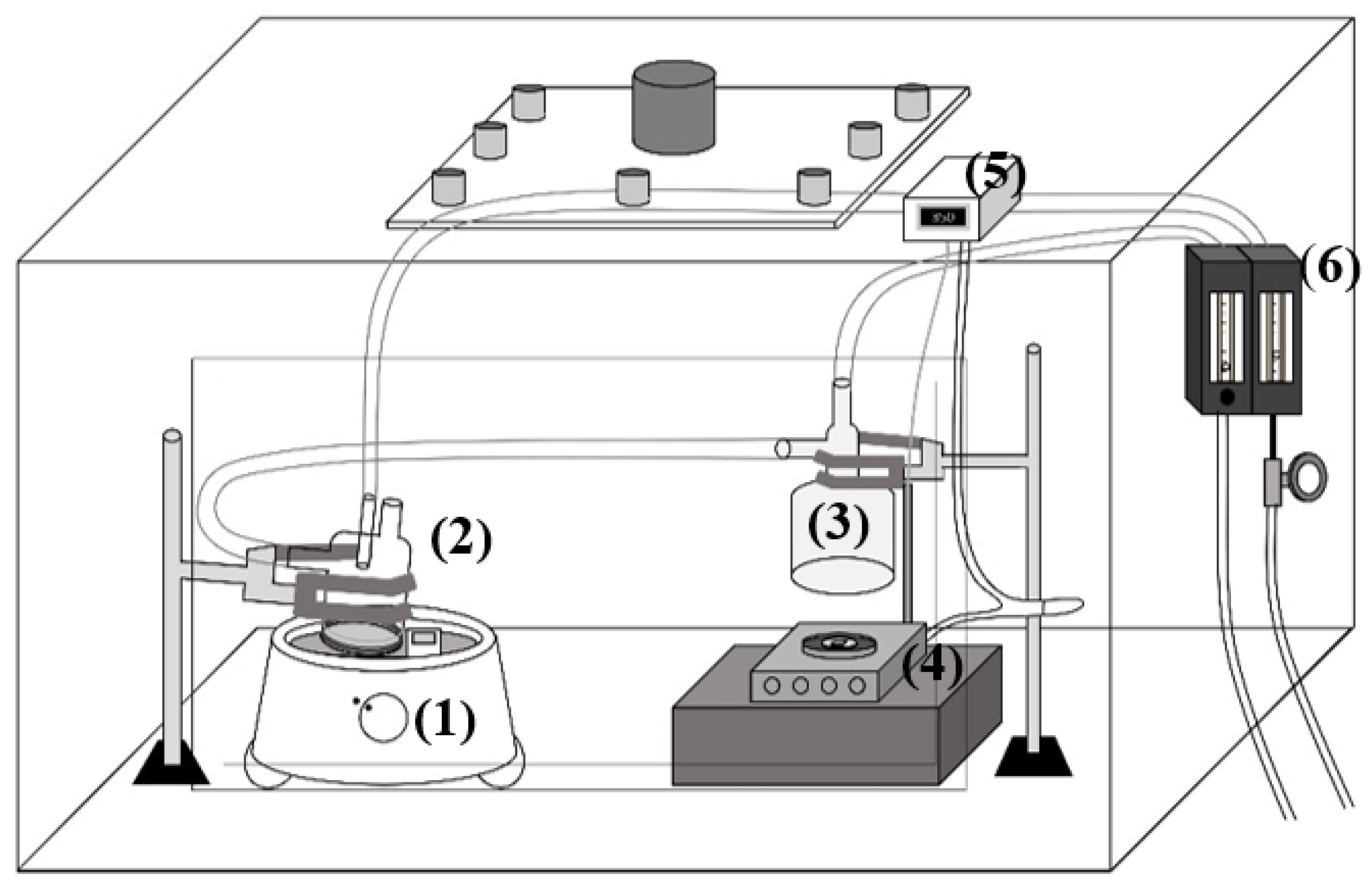
2. Experimental Details

2.1. Substrate Preparation

To carry out a complete characterization of our depositions, we grew our ZnO:Al thin films on glass, fused silica, and sodium chloride (NaCl) substrates. Glass and fused silica substrates were used for optical and electrical characterization. The NaCl substrates allowed us to carry out an exhaustive study of the nanostructural characteristics by scanning and transmission electron microscopy [28,29].
For the cleaning process of the glass and fused silica substrates, we follow our own methodology that has been previously reported [30,31] and that consists of ultrasonic baths with different solutions, each lasting 5 min at room temperature in the following order: (a) trichloroethylene to remove any grease; (b) methanol (CH4O) to remove trichloroethylene residues; (c) acetone (C3H6O) to remove organic particles and (d) methanol to remove acetone residues. Finally, we use high-pressure nitrogen (N2) jets to dry the substrates before use.

2.2. Spray Pyrolysis Deposition Process

For the growth of our TCOs, a Low-cost Own-designed Spray Pyrolysis System (LOSPS) was used assisted by ultrasound, whose schematic diagram is shown in Figure 1. We used ultra-high purity nitrogen (99.999%) as a working gas (drag and director). The precursor solution was made up of zinc acetate dihydrate [Zn(CH3COO)2·2H2O] (0.2 M) plus 3 at.% aluminum acetyl acetonate [Al(C5H7O2)3] (0.2 M). Both reagents were diluted in 8.7 parts of anhydrous methanol, 1 part deionized water, and 0.3 parts acetic acid (CH3COOH). CH3COOH plays an essential role in stabilizing the precursor solution, which exhibits a content of 3% Al by volume. Once prepared, the precursor solution was stirred at room temperature for 10 min.
To determine the optimal deposition temperature, we performed a recursive deposition-characterization study with an initial temperature of 300 °C and increments of 10 °C. The initial temperature was set at 300 °C because this is the lowest temperature at which it is possible to recover aluminum from [Al(C5H7O2)3] [16]. Meanwhile, the deposition time was determined by making a set of 58 thin films with different deposition times. We start with a 1 min growth and end with a 30 min growth in 30 s intervals. This set of thin films allowed us to identify the appropriate time to obtain a ZnO:Al TCO that exhibited optimal transmittance and conductivity. Consequently our best TCOs were grown at a temperature of 380 °C for 16 min. More details on the principles of the ultrasonic spray pyrolytic (USP) technique can be found elsewhere [32].
Our LOSPS is mounted inside a transparent acrylic box. The box is connected to an extractor to evacuate the remaining gases from pyrolysis. The system comprises a medical-grade ultrasonic atomizer actuated by a piezoelectric vibrating at 1.7 MHz. The precursor solution is placed inside a custom-designed “atomization cylinder” made of glass. The atomizing cylinder interacts with the water from the ultrasonic atomizer through a plastic membrane. This way, not only the water contained in the ultrasonic sprayer is atomized, but also the precursor solution contained in the atomization cylinder. The pulverized precursor solution is transported from the atomization cylinder through a corrugated fluoropolymer tube employing a controlled flow of N2 regulated by a 65 mm Cole-Parmer model PMR1-010404 flowmeter (Cole-Parmer, Vernon Hills, IL, USA). At the end of the fluoropolymer tube is another glass device called a “deposition hood.” When the precursor solution is in the deposition hood, it is forced to the substrate surface by another controlled flow of N2 regulated by a 65-mm Cole-Parmer flowmeter with valve model PMR1-010273. The substrate is placed on an aluminum nitride thermal plate that floats in a tin bath inside a stainless steel muffle equipped with five 500 W resistances. The temperature of the muffle is regulated through an Autonics temperature controller with solid state relay model TCN4S-24R (Autonics, Busan, Republic of Korea) to operate in the ambient to 900 °C range.

2.3. Characterization Instruments

Transmittance measurement was carried out at a normal angle of incidence using a Cary 5000 UV-Vis-NIR spectrometer (Agilent Technologies, Santa Clara, CA, USA) equipped with a dedicated deuterium lamp for the ultra-violet (UV) section. All reported spectra have a resolution of 1 nm, and the spectral range studied is from 310 nm to 1200 nm. The instrument features a lamp switch and a detector switch at 350 and 800 nm, respectively.
We use an Ossila four-point test system (Ossila Ltd., Sheffield, UK) that uses the Van der Pauw method to determine layer resistance for electrical characterization. The thickness of films on glass, fused silica, and graphene substrates was determined using the Manifacier method [33] using the UV-Vis spectra of each sample (with “Vis” denoting “visible”). Mesoscopic characterization was carried out using a high-resolution Schottky JEOL-JSM-7800F scanning electron microscope (SEM) (Japan Electron Optics Laboratory Co. Ltd., Akishima, Tokyo) with field emission operated in a voltage range between 1 and 15 kV. While for the nanostructural characterization, a JEOL JEM-2010F FastTEM transmission electron microscope (TEM) (Japan Electron Optics Laboratory Co. Ltd., Akishima, Tokyo) operated at 200 kV was used, with which the films deposited on NaCl substrates were studied, performing a detachment process carried out by dissolution of the substrate in distilled water. In addition, Bruker D8 Discover equipment (Bruker Corporation, Billerica, MA, USA) was used to carry out its study by X-ray diffraction (XRD).

3. Results

Approximately one hundred and fifty ZnO:Al depositions were made on glass and fused silica substrates to find the most suitable parameters to obtain competitive electro-optical characteristics and high reproducibility. Our LOSPS showed reproducibility in our depositions’ electric and optical traits.

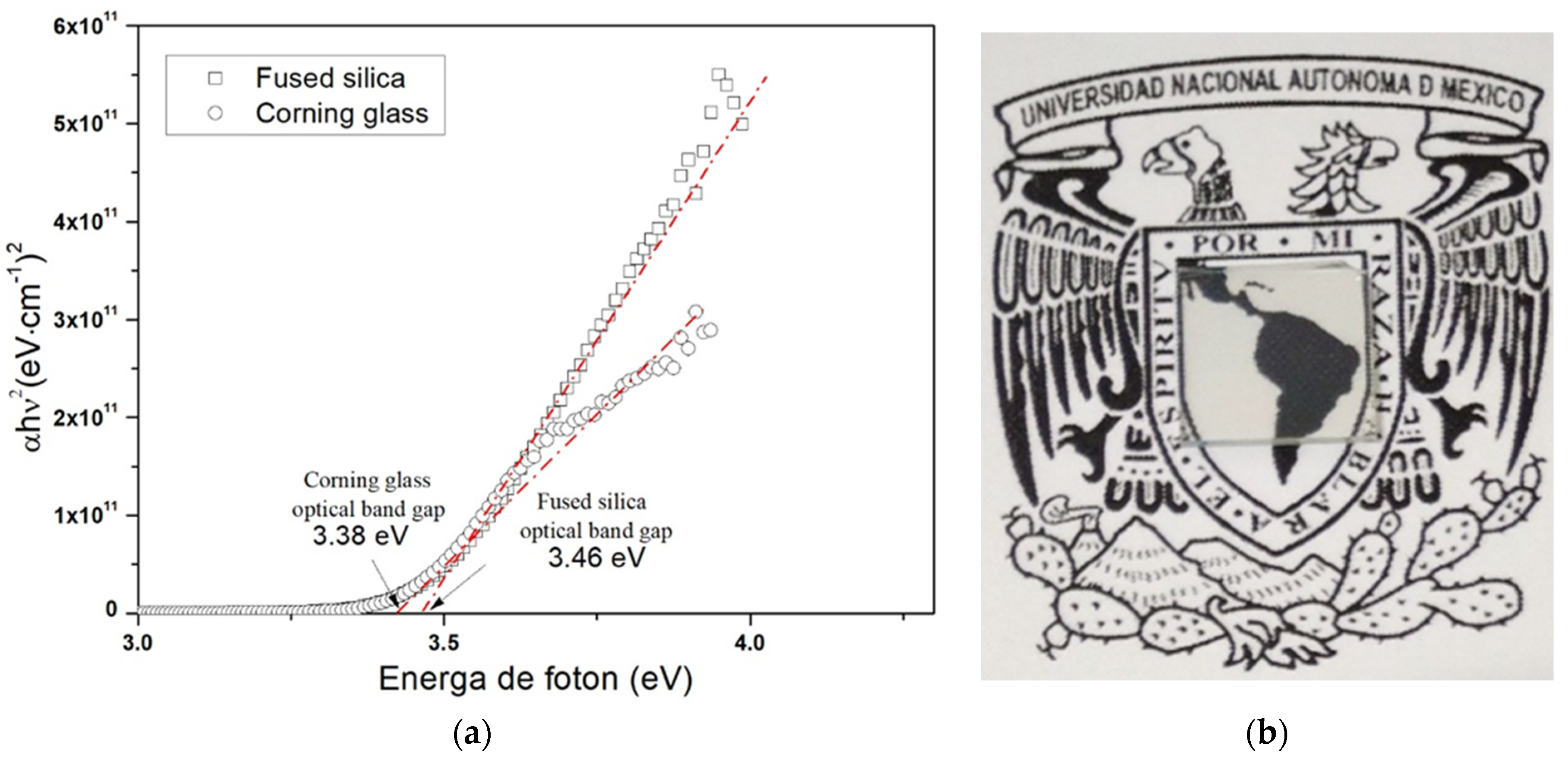
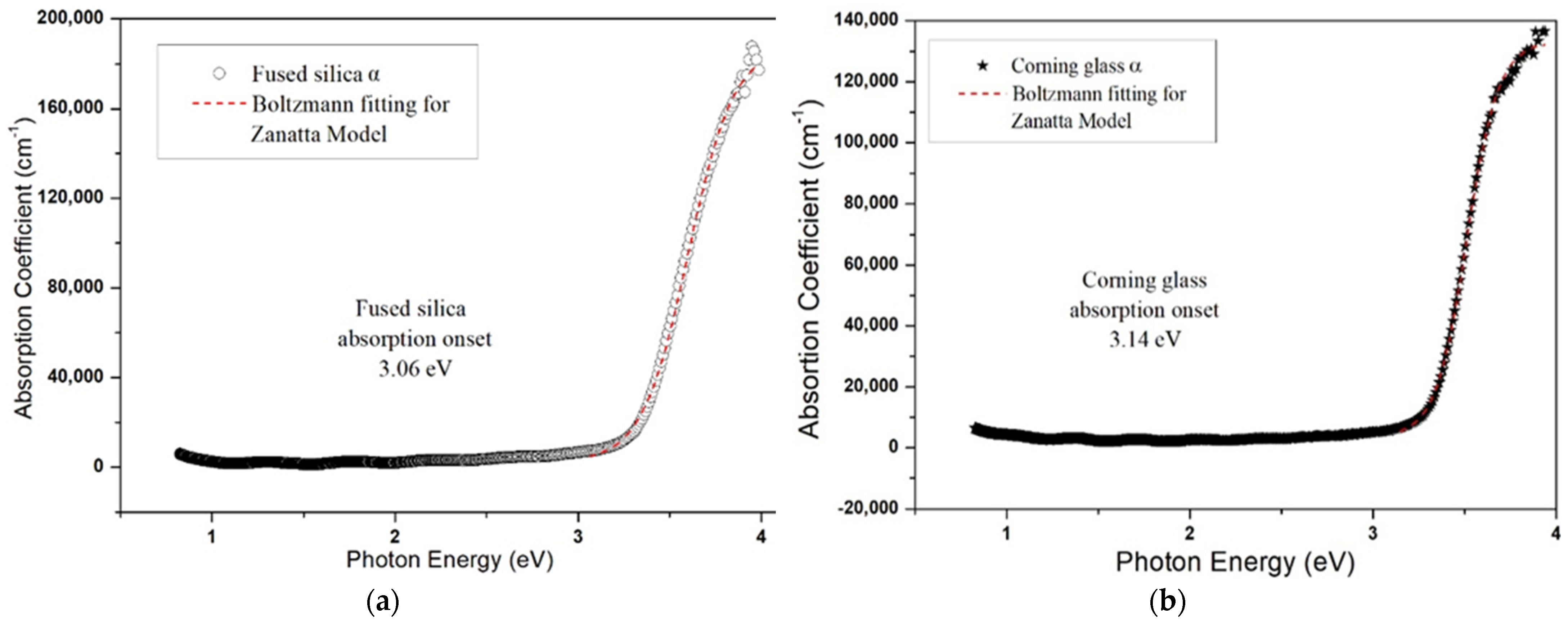
3.1. Optical Characterization

The low spatial resolution of the spectrometer allows collective phenomenological detection. The equipment’s beam excites millions of aluminum-doped zinc oxide crystallites simultaneously. Therefore, by measuring three different points on each sample, it is possible to determine the uniformity in transmittance of the thin films.
Figure 2 shows the transmittance spectra of the films deposited on fused silica and glass. On the other hand, optical analysis of the deposits made on salt could not be performed due to the opacity of the substrate. A detector shift at 800 nm explains the discontinuity of the plots at this value.

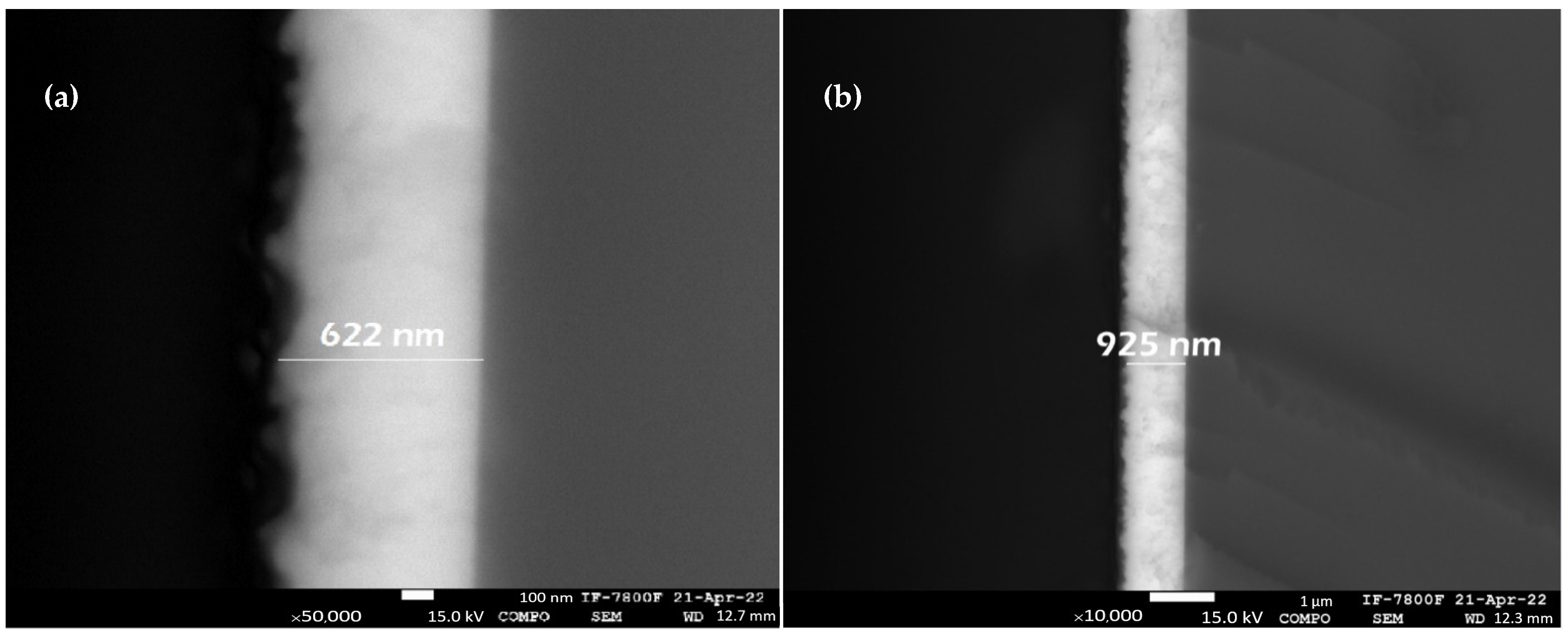
3.2. Deposition Thicknesses

The Manifacier method allows the thickness of a thin film to be determined from its transmittance spectrum. Using the spectra in Figure 2, we calculate that the thickness of the thin film deposited on glass is 919 ± 35 nm, while the thickness of the film grown on fused silica is 642 ± 34 nm. In Figure 3 presents cross-sectional micrographs of the deposited films, in which the thickness of the film is indicated. One can observe an exceptionally good concordance between the thicknesses obtained by scanning electron microscopy and those calculated through the Manifacier method.

3.3. Electrical Characterization

To evaluate and compare the quality and behavior of our thin films, Haacke’s high-resolution figure of merit (ΦH-HR) [34],
Φ H HR = T avg R s n   ,
is applied.
In Equation (1), the value of n varies depending on the pretended application to the TCO. The Tavg and Rs values are the average transmittance and sheet resistance, respectively. In this study, wavelengths from 380 to 800 nm were used for calculating Tavg, taken directly from the optical characterization results of Section 3.2. On the other hand, the Rs can be evaluated as
R s = ρ t   ,
where ρ is the resistivity and t is the thin film thickness. For small values of n, Rs has a more significant influence when evaluating the quality of a certain TCO. However, increasing n gives greater weight to Tavg. In the current study, the values of ΦH-HR are evaluated with n = 10, 12, and 20 to assess the films’ ability to be used in diverse applications.
Table 1 presents the determined optical transmittance and sheet resistance of our TCOs deposited on glass and fused silica. The value of the figure of merit is also reported for n = 10, 12, and 20.
Transparent semiconductors have wide enough bandgaps to allow much of the visible light to pass through the material. The most widely used method to experimentally determine the optical absorption band gap (Ebg) is the Tauc model [35,36,37], which is expressed as
( α E fot ) = D ( E fot E bg ) n / 2   ,
where D is a constant, Efot = , α is the absorption coefficient, h is the Planck’s constant, ν is light frequency, and n = 4 for direct transitions.
Figure 4 shows the Tauc scattering plot of αhν2 against photon energy for the film deposited on fused silica (squares) and the film deposited on glass (circles). It is possible to identify that the ZnO:Al film deposited on fused silica has a band gap of 3.38 eV, while the film deposited on glass has a band gap of 3.46 eV. This slight difference between bandgaps is briefly aborded in Section 4.
It is also helpful to calculate the absorption onset of our films. For this purpose, the Zanatta model [38] was used. Figure 5 shows a scattering plot of α versus photon energy for (a) ZnO:Al film deposited on glass and (b) ZnO:Al film deposited on a fused silica substrate. The red dotted lines represent the Sigmoid–Boltzmann fit for each TCO. Through this, it is possible to identify an absorption onset of 3.06 eV and 3.14 eV for the films on fused silica and glass, respectively. The fact that the start of absorption has a value below the gap calculated by Tauc is indicative of the possible presence of band tails or localized levels in the band gap of the ZnO: Al films obtained.

3.4. Nanostructural Characterization

In this section, the nanostructural traits of our ZnO:Al are determined, described, and, when possible, correlated with their optoelectrical characteristics: (1) X-ray diffraction and TEM characterizations to determine the zinc oxide crystalline phase and (2) SEM characterization to identify the surficial characteristics of our TCOs.

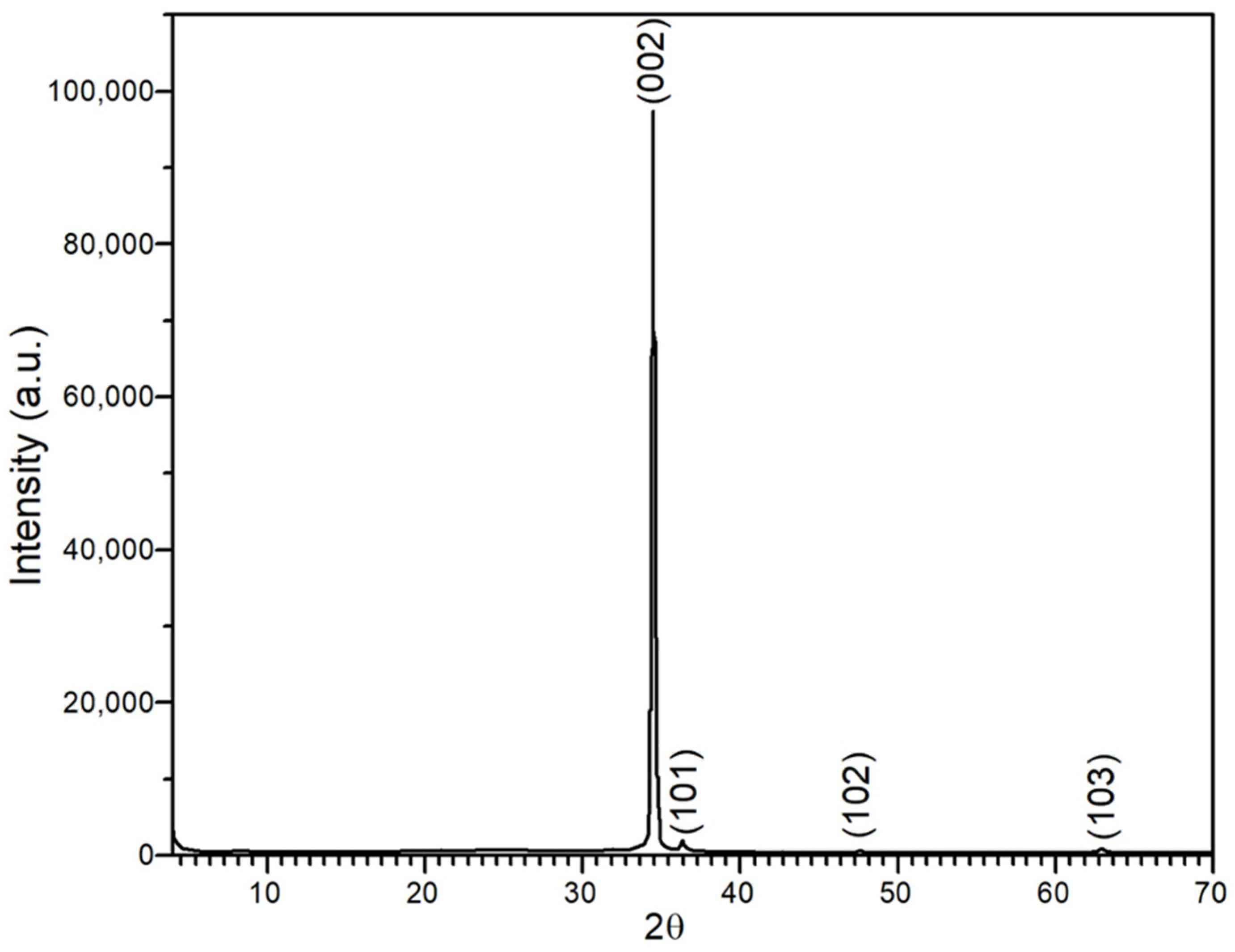
3.4.1. X-ray Diffraction Characterization

Figure 6 shows an X-ray diffractogram of the deposition made on glass. Based on the crystallographic file number 01-070-2551 of the Powder Diffraction File PDF-2-(2004) database [39], one can observe a polycrystalline structure with a considerably intense peak at 2θ = 34.7° associated with the crystal plane (002), where θ is the angle of incidence of the X-rays on the sample. The latter indicates a preferential growth oriented towards the c-axis corresponding to a hexagonal wurtzite structure, as expected for ZnO [26,39,40]. In addition, it presents small peaks at 2θ = 35.4°, 47.8° and 62.9° associated with the crystal (101), (102), and (103) planes, respectively.

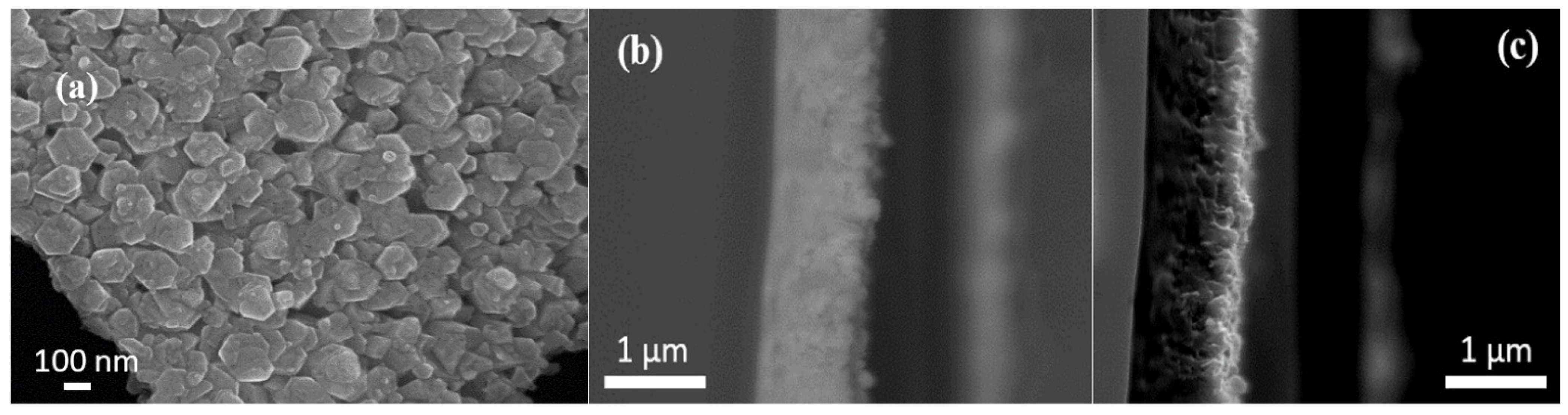
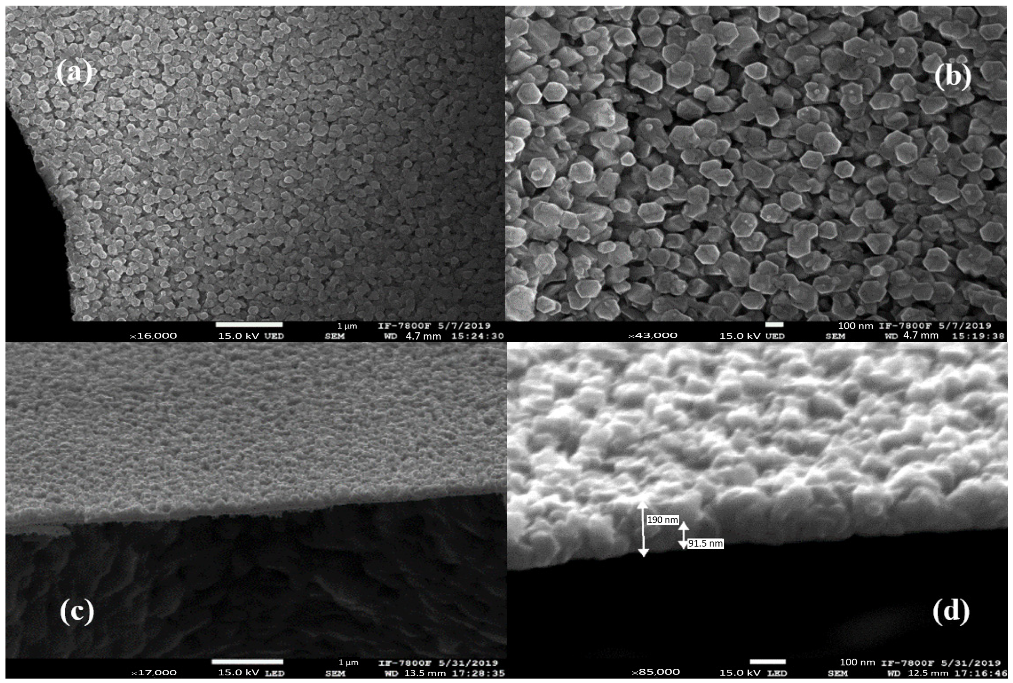
3.4.2. SEM Characterization

Figure 7a shows a micrograph at magnification 120,000× of the ZnO:Al film deposited on glass substrates at normal incidence where one can observe growths with hexagonal morphology, while Figure 7b,c show the thin film in cross-section at magnification 20,000× by secondary and backscattered electrons, respectively.
Figure 8 shows micrographs of the ZnO:Al film deposited on NaCl substrates. Micrographs Figure 8a,b show a morphology quite similar to that obtained in the growths made on glass (as shown in Figure 7a). Through micrographs Figure 8c,d made in cross-section, it was possible to obtain the thickness of the depositions given in Table 2.

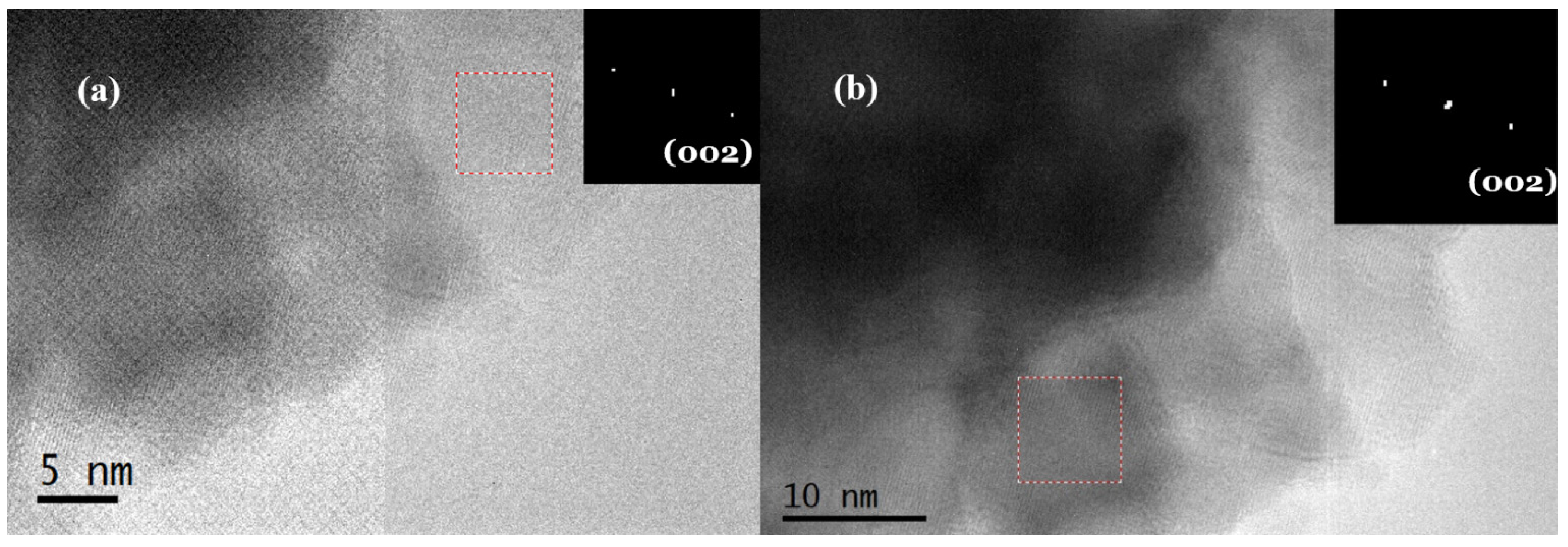
3.4.3. TEM Characterization

Through HRTEM (high resolution TEM), it was possible to study the crystals in the ZnO:Al thin films deposited on NaCl substrates by finding their preferential orientation. For this, the electron diffraction pattern of two micrographs obtained by HRTEM was obtained, allowing us to study the interplanar distances. The analysis was performed using the Digital Micrograph software 3.7.0 (Gatan Inc., Pleasanton, CA, USA) and the American Society for Testing Materials file 36-1451 (ASTM-file 36-1451) [51]. The micrograph in Figure 9a shows an interplanar distance of 2.67 Å, while the one in Figure 9b shows a distance of 2.6 Å. Both present a dominant orientation towards the (002) plane, that is, on the c axis, thus indicating that, in effect, it is ZnO:Al [51].

4. Discussion

The results shown above confirm that our LOSPS allows us to grow aluminum-doped zinc oxide thin films. X-ray diffraction showed that our ZnO:Al films exhibit a preferential orientation towards the c-axis, with a wurtzite hexagonal structure [52]. Likewise, through the HRTEM study, we obtained some of the interplanar distances in our samples which supports the claim that ZnO:Al thin films were grown with a preferential orientation. Meanwhile, through the SEM micrographs presented in Figure 3, it has been possible to corroborate that the growth of the ZnO:Al thin films is homogeneous all along the thickness of the film. As a consequence, one can conclude that simple enough deposition systems like the LOSPS here can grow high-performance ZnO:Al thin films and that LOSPS-like systems can be well scaled up for industrial use.
In Section 3.3, it was identified that the optical bandgap of the sample grown on the glass substrate varied slightly from the sample grown on fused silica. This difference could be due to the difference in thickness between the films. In this regard, we corroborate that the differences in bandgap in the two substrates studied are not greater than 300 meV when we grow films of the same thickness. Meanwhile, the presence of band tails could be explained by considering the Burstein-Moss shift produced by the increase in donors through ZnO doping [53].
The central premise of the current study is that high-yield ZnO:Al growth is possible using low-sophistication and low-cost equipment. Consequently, Table 2 compares the sheet resistance, average transmittance, and figure of merit values of our samples against five of the most referred studies regarding the growth of transparent conductive contacts of ITO, ZnO:Al, and ZnO:Ga.
From Table 2, one can find that the optoelectrical characteristics of the growths of this study are quite similar to those of high-performance TCOs manufactured using more sophisticated deposition techniques or even assisted by vacuum techniques. Also, it is worth noting that the best TCO here is only 14% less compelling than the best TCO in Table 2 which is made up of stoichiometric ITO. One can also observe that the most competitive TCO of this study is only 4% less efficient than a ZnO:Al TCO grown by magnetron sputtering.

5. Conclusions

We grew, with high reproducibility, aluminum-doped zinc oxide thin films by spray pyrolysis technique using a low-sophistication and low-cost equipment designed and manufactured by undergraduate students of our work group. We studied the growth of the ZnO:Al on three different substrates, glass, fused silica, and sodium chloride. We identify that the samples grown here present a hexagonal wurtzite structure with a preferential growth oriented towards the c-axis. Using UV-Vis spectroscopy, we determined an optical band gap of 3.38 eV and 3.46 eV with an absorption onset of 3.06 eV and 3.14 eV for the films deposited on fused silica and glass substrates, respectively.
Our best TCO used here features a thickness of approximately 650 nm, average transmittance of 80.2% in the visible range of the electromagnetic spectrum, and a sheet resistance of 31.93 Ω/□. This deposition is only 14% less efficient than a high-performance stoichiometric ITO TCO and only 4% less efficient than a ZnO:Al TCO grew by magnetron sputtering. Therefore, we consider that our growth represents a genuine alternative to commercial TCOs of ITO.

Author Contributions

Conceptualization, A.R.-G. and I.R.C.-C.; methodology, A.R.-G., I.R.C.-C., O.S.-D. and Y.H.W.; software, A.R.-G. and I.R.C.-C.; validation, A.R.-G. and A.L.P.-M.; formal analysis, A.R.-G., I.R.C.-C. and Y.H.W.; investigation, A.R.-G., G.L.-G., A.L.P.-M. and I.R.C.-C.; resources, A.R.-G.; data curation, I.R.C.-C., G.L.-G., O.S.-D., A.L.P.-M. and Y.H.W.; writing—original draft preparation, A.R.-G., I.R.C.-C., Y.H.W. and A.L.P.-M.; writing—review and editing, A.R.-G., I.R.C.-C. and A.L.P.-M.; visualization, A.R.-G.; supervision, A.R.-G.; project administration, A.R.-G.; funding acquisition, A.R.-G. All authors have read and agreed to the published version of the manuscript.

Funding

Ivan Ricardo Cisneros-Contreras acknowledges the Consejo Nacional de Ciencia y Tecnología—México for the doctoral scholarship, CVU No. 781505. All funding for the realization and publication of this research work came from the projects: (a) PAPIIT-UNAM project number IN109020, (b) PAPIIT-UNAM project number IN111723, (Mexico City, Mexico), and (c) CONACYT—Apoyos para Adquisición y Mantenimiento de Infraestructura en Instituciones y Laboratorios de Investigación Especializada 2019, project number 299881 (under the technical administration of Arturo Rodríguez-Gómez).

Data Availability Statement

Not applicable.

Acknowledgments

The authors would like to acknowledge the support provided by Roberto Hernández Reyes, Samuel Tehuacanero Cuapa, and Juan Gabriel Morales Morales for technical assistance with TEM (transmission electron microscope), SEM (scanning electron microscope), and in sample preparation, respectively.

Conflicts of Interest

The authors declare no conflict of interest.

References

  1. Aguilar del Valle, M.d.P.; Garrido, L.F.; Alonso-Huitrón, J.C.; Terrones Pacheco, L.; Cruz-Manjarrez, H.; Reyes-Gasga, J.; Pérez-Martínez, A.L.; Rodríguez-Gómez, A. Design, growth, and characterization of crystalline copper oxide p-type transparent semiconductive thin films with figures of merit suitable for their incorporation into translucent devices. Cryst. Growth Des. 2022, 22, 2168–2180. [Google Scholar] [CrossRef]
  2. Nateq, M.H.; Ceccato, R. Enhanced sol–gel route to obtain a highly transparent and conductive aluminum-doped zinc oxide thin film. Materials 2019, 12, 1744. [Google Scholar] [CrossRef] [PubMed] [Green Version]
  3. Portillo-Cortez, K.; Islas, S.R.; Serrano-Lázaro, A.; Ortiz, A.; García-Sánchez, M.F.; Alonso, J.C.; Martínez, A.; Ramos, C.; Dutt, A.; Santana, G. A novel soft deposition methodology for textured ZnO:Al thin films as efficient transparent conductive oxide layers. Appl. Surf. Sci. Adv. 2022, 9, 100255. [Google Scholar] [CrossRef]
  4. Zamani Meymian, M.-R.; Mousavi, M.-A.; Rabbani, M.; Fallah, M. Effects of thallium–aluminum-codoped zinc oxide thin film as a new transparent conducting oxide. Phys. Stat. Solidi 2021, 218, 2000619. [Google Scholar] [CrossRef]
  5. Muñoz-Rosas, A.; Rodríguez-Gómez, A.; Alonso-Huitrón, J. Enhanced electroluminescence from silicon quantum dots embedded in silicon nitride thin films coupled with gold nanoparticles in light emitting devices. Nanomaterials 2018, 8, 182. [Google Scholar] [CrossRef] [Green Version]
  6. Kurtaran, S. Al doped ZnO thin films obtained by spray pyrolysis technique: Influence of different annealing time. Opt. Mater. 2021, 114, 110908. [Google Scholar] [CrossRef]
  7. Das, A.; Das, G.; Kabiraj, D.; Basak, D. High conductivity along with high visible light transparency in Al implanted sol-gel ZnO thin film with an elevated figure of merit value as a transparent conducting layer. J. Alloys Compd. 2020, 835, 155221. [Google Scholar] [CrossRef]
  8. Zhao, K.; Xie, J.; Zhao, Y.; Han, D.; Wang, Y.; Liu, B.; Dong, J. Investigation on transparent, conductive ZnO:Al films deposited by atomic layer deposition process. Nanomaterials 2022, 12, 172. [Google Scholar] [CrossRef]
  9. Akhmedov, A.K.; Murliev, E.K.; Asvarov, A.S.; Muslimov, A.E.; Kanevsky, V.M. Transparent conductive indium zinc oxide films: Temperature and oxygen dependences of the electrical and optical properties. Coatings 2022, 12, 1583. [Google Scholar] [CrossRef]
  10. Pan, P.-C.; Koo, H.-S.; Chen, D.-X.; Chen, C.-M. Fabricating high-conduction and high-transparency tungsten-doped zinc oxide films by pulse laser deposition technique. Crystals 2022, 12, 1032. [Google Scholar] [CrossRef]
  11. Lin, Q.; Zhang, F.; Zhao, N.; Yang, P. Influence of annealing temperature on optical properties of sandwiched ZnO/Metal/ZnO transparent conductive thin films. Micromachines 2022, 13, 296. [Google Scholar] [CrossRef] [PubMed]
  12. Zdyb, A.; Krawczak, E.; Gułkowski, S. The influence of annealing on the properties of ZnO:Al layers obtained by RF magnetron sputtering. Opto-Electron. Rev. 2018, 26, 247–251. [Google Scholar] [CrossRef]
  13. Kim, H.; Gilmore, C.M.; Piqué, A.; Horwitz, J.S.; Mattoussi, H.; Murata, H.; Kafafi, Z.H.; Chrisey, D.B. Electrical, optical, and structural properties of indium–tin–oxide thin films for organic light-emitting devices. J. Appl. Phys. 1999, 86, 6451–6461. [Google Scholar] [CrossRef]
  14. Peng, S.; Wang, W.; Yao, T.; Guan, M.; Gan, Z.; Chu, J.; Gai, L. Excellent properties of Ga-doped ZnO film as an alternative transparent electrode for thin-film solar cells. Int. J. Appl. Glas. Sci. 2022, 14, 133–139. [Google Scholar] [CrossRef]
  15. Barman, B.; Swami, S.K.; Dutta, V. Fabrication of highly conducting ZnO/Ag/ZnO and AZO/Ag/AZO transparent conducting oxide layers using RF magnetron sputtering at room temperature. Mater. Sci. Semicond. Process. 2021, 129, 105801. [Google Scholar] [CrossRef]
  16. Rivera, M.J.; Ramírez, E.B.; Juárez, B.; González, J.; García-León, J.M.; Escobar-Alarcón, L.; Alonso, J.C. Low temperature-pyrosol-deposition of aluminum-doped zinc oxide thin films for transparent conducting contacts. Thin Solid Films 2016, 605, 108–115. [Google Scholar] [CrossRef]
  17. Marouf, S.; Beniaiche, A.; Kardarian, K.; Mendes, M.J.; Sanchez-Sobrado, O.; Águas, H.; Fortunato, E.; Martins, R. Low-temperature spray-coating of high-performing ZnO:Al films for transparent electronics. J. Anal. Appl. Pyrolys. 2017, 127, 299–308. [Google Scholar] [CrossRef]
  18. Ghosh, S.; Mallick, A.; Dou, B.; van Hest, M.F.A.M.; Garner, S.M.; Basak, D. A novel blanket annealing process to achieve highly transparent and conducting Al doped ZnO thin films: Its mechanism and application in perovskite solar cells. Sol. Energy 2018, 174, 815–825. [Google Scholar] [CrossRef]
  19. Koralli, P.; Fiat Varol, S.; Mousdis, G.; Mouzakis, D.E.; Merdan, Z.; Kompitsas, M. Comparative studies of undoped/Al-doped/In-doped ZnO transparent conducting oxide thin films in optoelectronic applications. Chemosensors 2022, 10, 162. [Google Scholar] [CrossRef]
  20. Sahu, D.R.; Lin, S.-Y.; Huang, J.-L. Improved properties of Al-doped ZnO film by electron beam evaporation technique. Microelectron. J. 2007, 38, 245–250. [Google Scholar] [CrossRef]
  21. Ali, H.M.; Abd El-Raheem, M.M.; Megahed, N.M.; Mohamed, H.A. Optimization of the optical and electrical properties of electron beam evaporated aluminum-doped zinc oxide films for opto-electronic applications. J. Phys. Chem. Solids 2006, 67, 1823–1829. [Google Scholar] [CrossRef]
  22. Bizarro, M. High photocatalytic activity of ZnO and ZnO:Al nanostructured films deposited by spray pyrolysis. Appl. Catal. B Environ. 2010, 97, 198–203. [Google Scholar] [CrossRef]
  23. Biswal, R.; Maldonado, A.; Vega-Pérez, J.; Acosta, D.; De La Luz Olvera, M. Indium doped ainc oxide thin films deposited by ultrasonic chemical spray technique, starting from zinc acetylacetonate and indium chloride. Materials 2014, 7, 5038–5046. [Google Scholar] [CrossRef] [PubMed] [Green Version]
  24. Schuler, T.; Aegerter, M. Optical, electrical and structural properties of sol gel ZnO:Al coatings. Thin Solid Films 1999, 351, 125–131. [Google Scholar] [CrossRef] [Green Version]
  25. Al-Ghamdi, A.A.; Al-Hartomy, O.A.; El Okr, M.; Nawar, A.M.; El-Gazzar, S.; El-Tantawy, F.; Yakuphanoglu, F. Semiconducting properties of Al doped ZnO thin films. Spectrochim. Acta Part A Mol. Biomol. Spectrosc. 2014, 131, 512–517. [Google Scholar] [CrossRef]
  26. Rozati, S.M.; Akesteh, S. Characterization of ZnO:Al thin films obtained by spray pyrolysis technique. Mater. Charact. 2007, 58, 319–322. [Google Scholar] [CrossRef]
  27. Jayathilake, D.; Nirmal Peiris, T. Overview on transparent conducting oxides and state of the art of low-cost doped ZnO systems. Sci. Forec. J. Mater. Chem. Engin. 2018, 1, 1004. Available online: https://scienceforecastoa.com/Articles/SJMCE-V1-E1-1004.pdf (accessed on 25 November 2020).
  28. Aguilar-Del-Valle, M.d.P.; Cruz-Manjarrez, H.; Rodríguez-Gómez, A. Simple fabrication and characterization of an aluminum nanoparticle monolayer with well-defined plasmonic resonances in the far ultraviolet. Metals 2018, 8, 67. [Google Scholar] [CrossRef] [Green Version]
  29. Rodríguez-Gómez, A.; Moreno-Rios, M.; García-García, R.; Pérez-Martínez, A.L.; Reyes-Gasga, J. Role of the substrate on the growth of silicon quantum dots embedded in silicon nitride thin films. Mater. Chem. Phys. 2018, 208, 61–67. [Google Scholar] [CrossRef]
  30. Rodríguez, A.; Arenas, J.; Pérez-Martínez, A.L.; Alonso, J.C. Role of ammonia in depositing silicon nanoparticles by remote plasma enhanced chemical vapor deposition. Mater. Lett. 2014, 125, 44–47. [Google Scholar] [CrossRef]
  31. Muñoz-Rosas, A.L.; Rodríguez-Gómez, A.; Arenas-Alatorre, J.A.; Alonso-Huitrón, J.C. Photoluminescence enhancement from silicon quantum dots located in the vicinity of a monolayer of gold nanoparticles. RSC Adv. 2015, 5, 92923–92931. [Google Scholar] [CrossRef]
  32. Zaiour, A.; Benhaya, A.; Bentrcia, T. Impact of deposition methods and doping on structural, optical and electrical properties of ZnO-Al thin films. Optik 2019, 186, 293–299. [Google Scholar] [CrossRef]
  33. Manifacier, J.C.; Gasiot, J.; Fillard, J.P. A simple method for the determination of the optical constants n, k and the thickness of a weakly absorbing thin film. J. Phys. E 1976, 9, 1002–1004. [Google Scholar] [CrossRef]
  34. Cisneros-Contreras, I.R.; Muñoz-Rosas, A.L.; Rodríguez-Gómez, A. Resolution improvement in Haacke’s figure of merit for transparent conductive films. Results Phys. 2019, 15, 102695. [Google Scholar] [CrossRef]
  35. Feng, Y.; Lin, S.; Huang, S.; Shrestha, S.; Conibeer, G. Can Tauc plot extrapolation be used for direct-band-gap semiconductor nanocrystals? J. Appl. Phys. 2015, 117, 125701. [Google Scholar] [CrossRef]
  36. Dolgonos, A.; Mason, T.O.; Poeppelmeier, K.R. Direct optical band gap measurement in polycrystalline semiconductors: A critical look at the Tauc method. J. Solid State Chem. 2016, 240, 43–48. [Google Scholar] [CrossRef] [Green Version]
  37. Mergen, Ö.B.; Arda, E. Determination of optical band gap energies of CS/MWCNT bio-nanocomposites by Tauc and ASF Methods. Synth. Met. 2020, 269, 116539. [Google Scholar] [CrossRef]
  38. Zanatta, A.R. Revisiting the optical bandgap of semiconductors and the proposal of a unified methodology to its determination. Sci. Rep. 2019, 9, 11225. [Google Scholar] [CrossRef] [Green Version]
  39. Bacaksiz, E.; Aksu, S.; Yilmaz, S.; Parlak, M.; Altunbaş, M. Structural, optical and electrical properties of Al-doped ZnO microrods prepared by spray pyrolysis. Thin Solid Films 2010, 518, 4076–4080. [Google Scholar] [CrossRef]
  40. Pandey, R.; Yuldashev, S.; Nguyen, H.D.; Jeon, H.C.; Kang, T.W. Fabrication of aluminium doped zinc oxide (AZO) transparent conductive oxide by ultrasonic spray pyrolysis. Curr. Appl. Phys. 2012, 12, S56–S58. [Google Scholar] [CrossRef]
  41. Alam, M.J.; Cameron, D.C. Optical and electrical properties of transparent conductive ITO thin films deposited by sol-gel process. Thin Solid Films 2000, 377–378, 455–459. [Google Scholar] [CrossRef]
  42. Benamar, E.; Rami, M.; Messaoudi, C.; Sayah, D.; Ennaoui, A. Structural, optical and electrical properties of indium tin oxide thin films prepared by spray pyrolysis. Sol. Energy Mater. Sol. Cells 1999, 56, 125–139. [Google Scholar] [CrossRef]
  43. Snure, M.; Tiwari, A. Structural, electrical, and optical characterizations of epitaxial Zn1−xGaxO films grown on sapphire (0001) substrate. J. Appl. Phys. 2007, 101, 124912. [Google Scholar] [CrossRef] [Green Version]
  44. Ramakrishna Reddy, K.T.; Miles, R.W. Growth and characterization of sprayed ZnO:Ga thin films. J. Mater. Sci. Lett. 1998, 17, 279–281. [Google Scholar] [CrossRef]
  45. Wang, Y.; Xu, G.; Yang, J.; Mao, W.; Wang, J.; Liu, Z.; Dong, Y.; Yang, S.; Li, J. Fabrication of AZO and FAZO films using low-cost spin-coating method. Opt. Mater. 2022, 126, 112204. [Google Scholar] [CrossRef]
  46. Koseoglu, H.; Turkoglu, F.; Kurt, M.; Yaman, M.D.; Akca, F.G.; Aygun, G.; Ozyuzer, L. Improvement of optical and electrical properties of ITO thin films by electro-annealing. Vacuum 2015, 120, 8–13. [Google Scholar] [CrossRef] [Green Version]
  47. Winkler, N.; Wibowo, A.; Kubicek, B.; Kautek, W.; Ligorio, G.; List-Kratochvil, E.; Dimopoulos, T. Rapid processing of In-doped ZnO by spray pyrolysis from environment-friendly precursor solutions. Coatings 2019, 9, 245. [Google Scholar] [CrossRef] [Green Version]
  48. Dimova-Malinovska, D.; Tzenov, N.; Tzolov, M.; Vassilev, L. Optical and electrical properties of R.F. magnetron sputtered ZnO:Al thin films. Mater. Sci. Engin. B 1998, 52, 59–62. [Google Scholar] [CrossRef]
  49. Dong, L.; Zhu, G.S.; Xu, H.R.; Jiang, X.P.; Zhang, X.Y.; Zhao, Y.Y.; Yan, D.L.; Yuan, L.; Yu, A.B. Preparation of indium tin oxide (ITO) thin film with (400) preferred orientation by sol–gel spin coating method. J. Mater. Sci. Mater. Electron. 2019, 30, 8047–8054. [Google Scholar] [CrossRef]
  50. Sofi, A.H.; Shah, M.A.; Asokan, K. Structural, optical and electrical properties of ITO thin Films. J. Electron. Mater. 2018, 47, 1344–1352. [Google Scholar] [CrossRef]
  51. Seeber, W.; Abou-Helal, M.; Barth, S.; Beil, D.; Höche, T.; Afify, H.; Demian, S. Transparent semiconducting ZnO:Al thin films prepared by spray pyrolysis. Mater. Sci. Semicond. Process. 1999, 2, 45–55. [Google Scholar] [CrossRef]
  52. Bizarro, M.; Sánchez-Arzate, A.; Garduño-Wilches, I.; Alonso, J.C.; Ortiz, A. Synthesis and characterization of ZnO and ZnO:Al by spray pyrolysis with high photocatalytic properties. Catal. Today 2011, 166, 129–134. [Google Scholar] [CrossRef]
  53. Rozati, S.M. Effect of film thickness on the physical properties of ZnO:Al thin films deposited using a spray pyrolysis technique. Can. J. Phys. 2008, 86, 379–382. [Google Scholar] [CrossRef]
Figure 1. Schematic diagram of LOSPS (Low-cost Own-designed Spray Pyrolysis System): ultrasonic atomizer (1) based on a SunShine medical humidifier that sprays the precursor solution inside the atomization cylinder (2) that communicates through a corrugated fluoropolymer tube with the deposition hood (3). The pulverized precursor solution is transported from (2) to (3) utilizing a flow of N2 called carrier gas. When the pulverized precursor solution is in (3), it is forced through a directing jet of nitrogen (N2) gas towards the surface of the substrate that is in a aluminum nitride thermal plate (4) that floats in a bath of liquid tin. The temperature of the muffle is regulated through an Autonics temperature controller (5) with solid state relay model TCN4S-24R. The drag and director flows are regulated by employing two Cole-Parmer flowmeters (6) through an Autonics temperature controller with solid state relay model TCN4S-24R to operate in the ambient to 900 °C range.
Physics 05 00004 g001
Figure 2. Transmittance spectrum of ZnO:Al thin films deposited on a glass substrate, a fused silica substrate, and a glass substrate. The spectrum exhibited for the fused silica substrate takes a range of wavelengths from 310 nm to 2300 nm, while that of glass only goes from 310 nm to 1500 due to the loss of information produced by the substrate.
Physics 05 00004 g002
Figure 3. Cross-sectional micrographs of (a) deposition made on a fused silica substrate and (b) deposition made on a glass substrate. A film thickness label is added to both micrographs.
Physics 05 00004 g003
Figure 4. (a) Tauc scattering of direct transitions for ZnO:Al deposited on fused silica substrate (squares) and glass substrate (circles). Linear fit extrapolation was taken over a range of 3.4 to 4 eV in both cases and is presented by a red dotted line. See text for details. (b) Photograph of ZnO:Al film deposited on glass substrate showing exceptionally good homogeneity at the macroscopic level.
Physics 05 00004 g004
Figure 5. Scatter plot of absorption coefficient against photon energy for ZnO:Al films deposited on (a) fused silica substrate and (b) glass substrate. A Sigmoid-Boltzmann fit for the absorption coefficient for each film is presented using a red line. The absorption onsets were determined to be 3.06 and 3.14 eV, respectively.
Physics 05 00004 g005
Figure 6. X-ray diffractogram of ZnO:Al deposited on glass. A very intense peak can be identified at 2θ = 34.7°, which is associated with the crystal plane (002) with θ the the angle of incidence of the X-rays on the sample. This reflection indicates a preferential growth oriented toward the c-axis, corresponding to a hexagonal wurtzite structure.
Physics 05 00004 g006
Figure 7. Micrograph of ZnO:Al thin films on glass (a) at normal incidence, (b) in cross-section with secondary electrons, and (c) in cross-section with backscattered electrons.
Physics 05 00004 g007
Figure 8. Micrograph of the deposition made on NaCl substrate (a) surface at magnification 16,000×, (b) surface at magnification 43,000×, (c) cross-section at magnification 17,000×, (d) cross-section at magnification 85,000×.
Physics 05 00004 g008
Figure 9. Micrographs of ZnO:Al film deposited on NaCl substrate and subsequently detached from it. The indexing of the electron pattern has been carried out on the areas delimited by a dotted line.
Physics 05 00004 g009
Table 1. Average transmittance, sheet resistance, and factor of merit (for n = 10, 12, and 20; see Equation (2)) of our best ZnO:Al TCO deposited on glass and fused silica.
SampleAverage
Transmittance (%)
Sheet Resistance
[ Ω ]
Φ H H R
[ Ω 1 10 ]
Φ H H R
[ Ω 1 12 ]
Φ H H R
[ Ω 1 20 ]
Glass75.719.056.459.265.4
Fused Silica80.231.957.060.167.4
Table 2. Comparison between our depositions and thirty of the most referred TCOs deposited through different deposition techniques.
MaterialDeposition Technique Thickness   [ n m ] Sheet
Resistance
[ Ω ]
Average
Transmittance
(%)
Φ H H R
[ Ω 1 10 ]
Φ H H R
[ Ω 1 12 ]
Φ H H R
[ Ω 1 20 ]
Reference
ZnO:Al-Tl1 at% of Tl to aluminum-doped zinc oxide (AZO)Sol-gel-spin coating19202.838576.677.980.7[4]
ITO-Sol-gel2501.508076.877.378.4[41]
ZnO:AlAnnealed at 550 °C with Zn filmDC magnetron sputtering3508.809072.475.180.7[18]
ITO-Spray pyrolysis5005.008572.474.378.4[42]
ZnO:GaPrepared on float glass at 400 °CMagnetron sputtering8255.508571.873.978.2[14]
Zn1−xGaxO1% of GaPulsed laser deposition2007.208771.473.878.8[43]
ZnO:Ga-Magnetron sputtering3007.338569.672.076.9[44]
ZnO:Al/Ag/ZnO:Al-Magnetron sputtering705.308067.769.673.6[15]
ZnO:AlPrepared on float glass at 400 °CMagnetron sputtering82510.808365.768.474.0[14]
ZnO/Ag/ZnO-Magnetron sputtering705.407865.967.871.7[15]
ZnO:Al-Magnetron sputtering221024.008864.067.575.1[12]
ZnO:AlFilms prepared at 450 °CSpin-coating54760.709361.665.975.6[45]
ZnO:In-Radio frequency magnetron sputtering3808.957761.864.169.0[9]
ITO-Electro annealing25615.007960.363.069.0[46]
ZnO:In-Ultrasonic spray pyrolysis180021.208058.962.068.7[47]
ZnO:Al-Magnetron sputtering40045.008558.161.970.3[48]
ZnO:Al-FFilms prepared at 450 °CSpin-coating62091.308956.460.970.7[45]
ZnO:AlFilms prepared below 390 °C and without subsequent annealingLow-cost, own-designed ultrasonic spray pyrolysis64231.008056.760.167.4This work
ZnO/Metal/ZnO50 nm ZnO/Ti/Cu/Ti/50 nm ZnOMagnetron sputtering706.606553.855.559.1[11]
ITO-Sol-gel-spin coating180230.008549.354.064.8[49]
ZnO:Al-Sol-gel-spin coating350156.008249.553.863.7[7]
ZnO/Metal/ZnO50 nm ZnO/Cu/50 nm ZnOMagnetron sputtering6010.106047.649.553.4[11]
ZnO:W1.0 wt% tungstenPulsed laser deposition86229.007543.647.757.2[10]
ZnO:In450 °C and a ratio of [In]/[In+Zn] = 3.0 at%Ultrasonic spray pyrolysis100034.206042.144.750.3[23]
ITO-Thermal evaporation150166.006036.039.246.5[50]
ZnO:AlFAr 5 sccm and 45 WDC magnetron sputtering516.86 × 1037531.035.948.2[3]
ZnO:AlThin films containing 2 at% AlSol–gel1063.84 × 1047927.532.846.7[2]
ZnO:Al-Sol-gel-spin coating2442.35 × 1068519.625.040.8[19]
ZnO:Al3%Atomic layer deposition185.56 × 1057520.024.938.7[8]
ZnO:In-Sol-gel-spin coating2453.51 × 1068518.824.240.0[19]
ZnO:Al3 h annealing (400 °C)Ultrasonic spray pyrolysis941.48 × 1065012.115.324.6[6]
Disclaimer/Publisher’s Note: The statements, opinions and data contained in all publications are solely those of the individual author(s) and contributor(s) and not of MDPI and/or the editor(s). MDPI and/or the editor(s) disclaim responsibility for any injury to people or property resulting from any ideas, methods, instructions or products referred to in the content.

