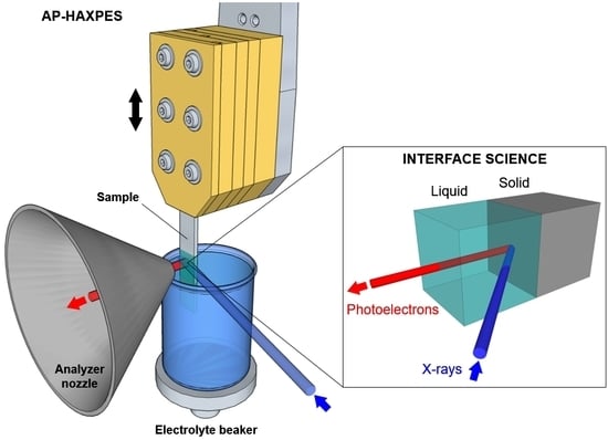
3.1. The Challenge of Preparing a Realistic Solid/Liquid Interface
The main challenge in the investigation of solid/liquid interfaces using a photon in/electron out technique lies in the preparation of the interface itself. The electron detection implies that the electrons ejected from the interfacial region need to penetrate through condensed phases whose thickness must be less than two to three times the electron inelastic mean free path (IMFP). Although the use of hard X-rays allows obtaining high photoelectron KEs (and therefore IMFPs), a photoelectron having a KE spanning from 2000 eV to 10000 eV is characterized by an IMFP on the order of tens of nanometers. This poses severe limitations and constraints in the preparation of the solid/liquid interface.
Currently, two different preparation and investigation approaches are used, which differ from each other for the side of the interface that is used for the X-ray incidence and electron detection [
9].
Photoelectron spectroscopy can be conducted from the solid side of the solid/liquid interface using few layer graphene membranes supporting the solid phase [
30,
31]. Although this technique is appealing for the fact that gases or liquids can be flown through the system thereby providing facile mass transport, it limits the investigation to thin solid films since the photo-emitted electrons must travel through the solid phase/graphene membrane to reach the photoelectron analyzer. For instance, a photoelectron travelling in Au with a KE of 500 and 5000 eV is characterized by an IMFP of about 0.8 and 4.2 nm, respectively. Using the definition of the information depth as three times the IMFP (i.e., the depth in the material at which 95% of the ejected photoelectrons are inelastically scattered in their path toward the surface), we find that the maximum probed thickness of Au achievable with soft (hard) X-rays is equal to about 2 nm (13 nm).
A second approach, using X-ray incidence and electron detection from the liquid side, requires the formation of a thin liquid layer atop the solid surface [
9]. This approach has the advantage of being able to investigate a broad range of solid materials of arbitrary thickness. This is particularly important for photoelectrochemical (PEC) interfaces, due to the diffusion length of the excited charge carriers (λ
CC) that can span from tens to hundreds of nm. This poses a constraint on the thickness (
t) of the investigated semiconductor, where
t ~ λ
CC. In addition, such approach is applicable to fundamental investigations at interfaces such as the probing of the electrical potential distribution simultaneously within the solid (i.e., band-bending) and the liquid side of the junction (the double/diffuse layer) [
13,
17].
Similar to the previous discussion, the maximum thickness of the liquid layer must be three times the photoelectron IMFP to allow the photoelectrons ejected from the interface to penetrate the liquid film, to cross the liquid/gas interface and finally to travel through the gas phase on their path toward the electron analyzer. Therefore, for photoelectrons traveling in water with a KE of 500 eV and 5000 eV, the maximum water thickness must be equal to about 6 nm and 38 nm, respectively.
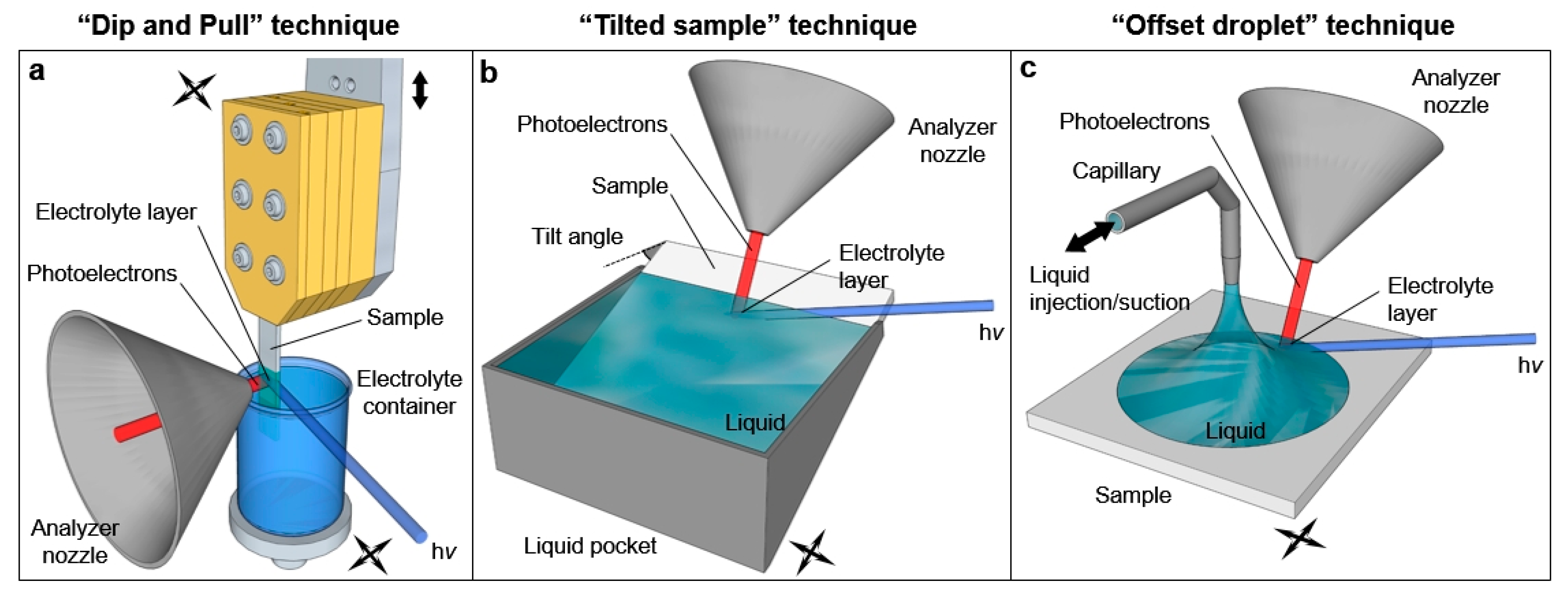
The preparation of liquid layers characterized by a thickness of the order of tens of nanometer and that are stable for the duration of the measurements (often several hours) is not straightforward and requires the development of novel techniques. As schematically reported in
Figure 2, three experimental procedures have been identified to obtain such “free-surface” liquid layers: the “emersion technique” (recently called ‘’dip and pull”,
Figure 2a), “the tilted sample” procedure (
Figure 2b) and the “offset droplet” method (
Figure 2c).
The “dip and pull” method was developed from the early works on the extended liquid meniscus of Bockris and Cahan [
32], Siegbahn [
33] and in particular by Hansen and Kolb [
34,
35,
36]. It obtains nanometer-thick liquid layers by partially extracting the sample from the liquid solution under controlled conditions (i.e., equilibrium between the liquid and its vapor at a given temperature, constant rate of pulling). This method will be discussed in detail in the next
Section 3.1.1.
In “the tilted sample” technique developed by Kötz and coworkers [
37], the liquid is contained in a pocket in which the sample is immersed with a tilt angle. This tilt creates a region at the boundary between the liquid free surface and the sample that can be positioned at the focal point of the analyzer and irradiated by the X-ray beam. The authors were able to detect the photoelectron spectra of the elements of the investigated ionic liquid (1-ethyl-3-methylimidazolium tetrafluoroborate) and of the Pt sample simultaneously in one survey spectrum, using the Al K
α emission line as excitation source [
37]. Similar to what has been described above, it is possible to create a stable evaporation/condensation equilibrium by dosing water in the analysis chamber to match the water vapor pressure above the liquid contained in the pocket, at the given temperature of the experiment.
Recently, Walton and coworkers developed instead an alternative way by using a fine capillary (100 μm internal diameter) to inject and control a droplet deposited in situ on the sample surface [
38]. Since an offset exists between the position of the capillary and the measurement spot, the authors named this technique as the “offset droplet” method. The capillary is connected with an external HPLC pump via a liquid feedthrough. By applying a fixed flow rate to the pump, the liquid can be directly introduced into the analysis chamber and deposited on the sample surface. After an initial transient in which the pressure in the analysis chamber will equilibrate to the liquid vapor tension, a steady-state condition can be reached by choosing an appropriate flow to counterbalance the evaporation rate. By rigidly moving the sample and the capillary, the droplet edge can be positioned at the intersection of the photon beam and the analyzer focus, enabling therefore photoemission experiments at the solid/liquid interface.
It is worth mentioning that the three aforementioned techniques do not allow a fine control of the liquid layer thickness, although it is possible to “select” the suitable thickness for the experimental purposes. With the “dip and pull” technique, it is possible to change the height of the measurement spot by changing the positions of the sample and liquid container with respect to the X-ray beam-analyzer focus intersection. The same procedure can be applied to the “tilted sample” and “offset droplet” techniques, by changing the tilt angle and the liquid injection/suction rate, respectively. The described procedure holds exclusively for wettable surfaces, where the contact angle
ψ at the liquid meniscus is smaller than 90° (indicating relatively intense interactions between the solid and the liquid). This poses a severe restriction on the type of samples/surfaces accessible using these techniques, due to the fact that no nanometric-thick continuous liquid layer can be formed on non-wettable surfaces (
ψ ≥ 90°). A practical example of this drawback will be given in
Section 3.3.
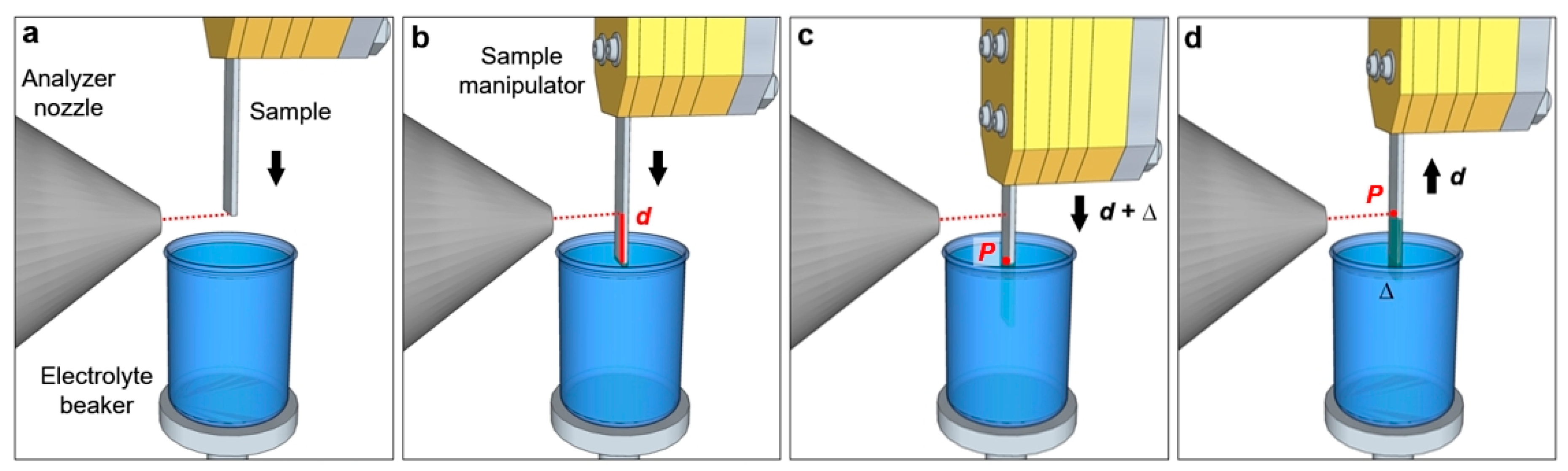
3.1.1. The “Dip and Pull” Method
Figure 3 reports a schematization of the “dip and pull” procedure. The sample is first placed in front of the analyzer nozzle, aligning its bottom edge with the nozzle aperture (
Figure 3a). The sample is then lowered till its bottom edge enters in contact with the liquid free surface in the electrolyte beaker (
Figure 3b). By measuring these two positions using the sample manipulator encoder, it is possible to get the value
d, which is the distance between the nozzle aperture and the free surface of the electrolyte (typically some millimeters). The sample is then immersed into the liquid by the same length, plus an additional portion ∆ (
Figure 3c). The sample is then retracted from the liquid by a distance
d, as reported in
Figure 3d. In this manner, the point
P that was previously placed at the liquid meniscus (liquid/gas interface) is now aligned with the nozzle aperture, thereby facilitating the search of the optimal liquid layer thickness. By scanning the region around
P (changing the height of the measurement spot as reported above) it is possible to find the suitable layer thickness for the experiment (in the case of AP-HAXPES the film thickness can span from few to some tens of nm).
The liquid film thickness depends on a number of factors and their corresponding interplays: on the wettability of the solid surface for a given liquid (i), the height of the measurement spot above the free surface of the bulk liquid (ii), the presence of an eventual temperature gradient between the two positions (iii), and the solvent evaporation rate (iv). To counterbalance water evaporation from both the liquid layer and the container, two options can be used: either dosing water in the analysis chamber through a valve connected with a heated external reservoir, or by introducing a second (larger) water volume within the analysis chamber. Both solutions work at pressures close to the water vapor pressure at room temperature (100% relative humidity, RH), thus generating a dynamic equilibrium at the thin liquid layer where the evaporation and condensation rates are the same. Then, by moving the sample (and the liquid container accordingly), the interface can be positioned at the intersection of the incident X-ray beam and the focal point of the electron analyzer, thereby enabling in situ photoemission measurements of the solid/liquid interface.
The “dip and pull” method can be also utilized to perform in situ (photo)electrochemical and photoemission measurements. Two additional electrodes can be mounted on the sample holder, leading to an effective three-electrode electrochemical cell [
11,
12,
13,
14,
15,
16,
17]. The bottom part of the electrodes (∆), being kept in the bulk electrolyte, provides the electrochemical continuity to apply a potential to the thin electrolyte layer on the sample (working electrode) surface, thus enabling the investigation of solid/liquid electrified interfaces [
11,
12,
13,
14,
15,
16,
17]. A drawback of this method (and, in general, of the “free-surface” liquid layer approach) is constituted by the mass transport limitation in the electrolyte layer, since the latter is effectively static in the direction parallel to the solid surface (with the exception of liquid flow due to eventual differences in the temperature between the electrolyte reservoir and the measurement spot above the liquid meniscus, causing thermo-capillary or Bénard–Marangoni convection). The mass transport limitations have been experimentally addressed in our recent works [
15,
39]. We have demonstrated that the liquid layer undergoes instability for faradaic reactions involving consumption of the electrolyte, such as during the oxygen evolution reaction (OER) in 1.0 M KOH aqueous solution [
39]. Holding the potential at the Pt working electrode at +1.93 V vs. RHE (reversible hydrogen electrode), we observed the loss of potential control within the liquid layer in less than 2 h from the beginning of the experiment [
39]. The loss of anodic polarization was assessed by the deviation of the binding energy (BE) shift of the O 1s liquid phase water (LPW) component and K 2p core levels from the applied OER potential, as a function of the observation time [
39]. The following mechanism is likely to occur: first, the hydroxyl anions are depleted from the thin liquid layer due to the ongoing oxidation to molecular oxygen. Second, the consequent decrease over time of the pH within the liquid layer leads to an increasing
IR drop, which is responsible for the observed BE deviation from the applied potential. Interestingly, after the loss of potential control occurred, we observed also an important decrease of the LPW signal mirrored by the K 2p intensity, thereby indicating a progressive thinning of the liquid layer. To estimate the diffusion time scale of the hydroxyl groups from the liquid meniscus through the liquid layer, we can use Fick’s first law of diffusion (Equation (2)). The distance
z of the liquid meniscus from the AP-HAXPES measurement position is typically about 0.8 mm, and the diffusion coefficient
D of hydroxyl anions in water at infinite dilution at room temperature is equal to 5.30 × 10
−5 cm
2 s
−1 [
40].
J║ represents the diffusional flux parallel to the sample surface, which is the amount of hydroxyl groups (
n, in mol) flowing through the liquid layer cross-section (
Σ) within the time ∆
t, whereas (
dC/
dz)
║ is the 1-dimensional concentration gradient within the liquid layer (parallel to the sample surface) between the measurement spot and the liquid meniscus. First, we take into account a liquid layer thickness of 20 nm, which is a typical value for the “dip and pull” technique, and 0.7 mm as the lateral dimension of the sample. The cross-section
Σ of the electrolyte film is therefore 0.7 cm × 20 × 10
−7 cm = 1.4 × 10
−6 cm
2. Secondly, let us define a complete depletion of hydroxyl within the liquid layer after a time ∆
t. This sets the concentration gradient (
dC/
dz)
║ to be linear between the measurement spot and liquid meniscus, where the OH
− concentration (C) is nominally equal to 1.0 M (1 mol L
−1). Therefore, (
dC/
dz)
║ = 1 mol L
−1/0.8 cm = 10
−3 mol cm
−3/0.8 cm = 1.25 × 10
−3 mol cm
−4. We can then determine the flux
J of hydroxyl through the cross section
Σ per unit time:
J║ =
n/(
Σ × ∆
t) = C ×
Σ ×
z/
Σ × ∆
t = C ×
z/∆
t = 10
−3 mol cm
−3 × 0.8 cm/∆
t = 8.0 × 10
−4 mol cm
−2/∆
t. Using Equation (2) we can calculate ∆
t, which is the time needed by the hydroxyl groups to diffuse from the liquid meniscus to replenish the solution volume within the thin electrolyte layer. ∆
t is found to be about 12 × 10
3 s (~3.3 h). This limitation in the ionic diffusion rate is confirmed by a recent study of Shavorskiy et al., where the authors observe a significant
IR drop in the liquid film at the hematite/liquid electrolyte interface under PEC conditions (for applied potentials above ~1.2 V vs. RHE) [
17]. This mass transport limitation has also an important effect on the achievable current densities within the liquid layer. In a recent study, we masked the bottom of a Pt sample immersed in KOH 1.0 M aqueous electrolyte and compared to an unmasked electrode [
15]. We determined that a bulk (unmasked) current density of about 1.0 mA cm
−2 under OER conditions corresponds to about 0.3 mA cm
−2 in the emersed part of the Pt surface [
15]. This observation was confirmed by the polarization resistance (R
p) for the masked and unmasked configurations, determined using electrochemical impedance spectroscopy (EIS) measurements. In line with the current densities results, the ratio between the two configuration R
p (unmasked to masked) was equal to 3.37 [
15]. It is important to highlight that it was not possible to completely avoid the contribution arising from the macroscopic liquid meniscus between the sample and the liquid free surface. Therefore, the actual current density at the AP-HAXPES measuring spot might be even lower. As a general remark, the interplay between the applied overpotential and the limitations in the mass transport kinetics through the liquid layer plays a crucial role during “dip and pull” experiments, and needs to be evaluated case by case (depending on the nature of the solid surface, the catalytic activity of the (photo)electrocatalyst etc.). Moreover, the electrode potential at the measuring spot must be corrected for the actual pH value (since an eventual concentration gradient leads to a pH gradient as well within the liquid layer). This can be performed by calculating the electrolyte/water ratio using the corresponding photoionization core levels (such as K 2p and O 1s for a KOH aqueous solution, as reported in reference [
15]).
The lowering of the reaction kinetics within the liquid layer due to the mass transport limitations can be exploited to investigate the evolution of the interfacial properties on a time scale accessible by AP-HAXPES (seconds). For instance, in a recent work we were able to monitor the light-induced formation of a bismuth phosphate (BiPO
4) layer atop a polycrystalline bismuth vanadate (BiVO
4) surface, working at the half-cell open circuit potential and in a phosphate-containing electrolyte layer with a thickness ranging between 24 and 32 nm [
41]. We found that the BiPO
4 formation was reversible upon restoring dark conditions. The BiPO
4 formation and dissolution kinetics have been characterized by fitting the temporal trend of the phosphate/water liquid phase (LPW) intensity ratio under visible light and dark conditions, respectively (the spectral components have been determined from the O 1s core level spectra acquired under light and dark conditions as a function of time). The retrieved time constants of the BiPO
4 formation and dissolution were found to be equal to 321 ± 61 s and 498 ± 89 s, respectively [
41].
Finally, a general challenge closely related to the use of the aforementioned methods concerns the enhancement of the photoelectron signal coming from the narrow interfacial region atop the solid and buried by the liquid side of the junction. In the next section, using a model solid/liquid junction and numerical simulations, we will address this point and assess the optimal X-ray energy that allows the enhancement of the interface photoelectron signal.
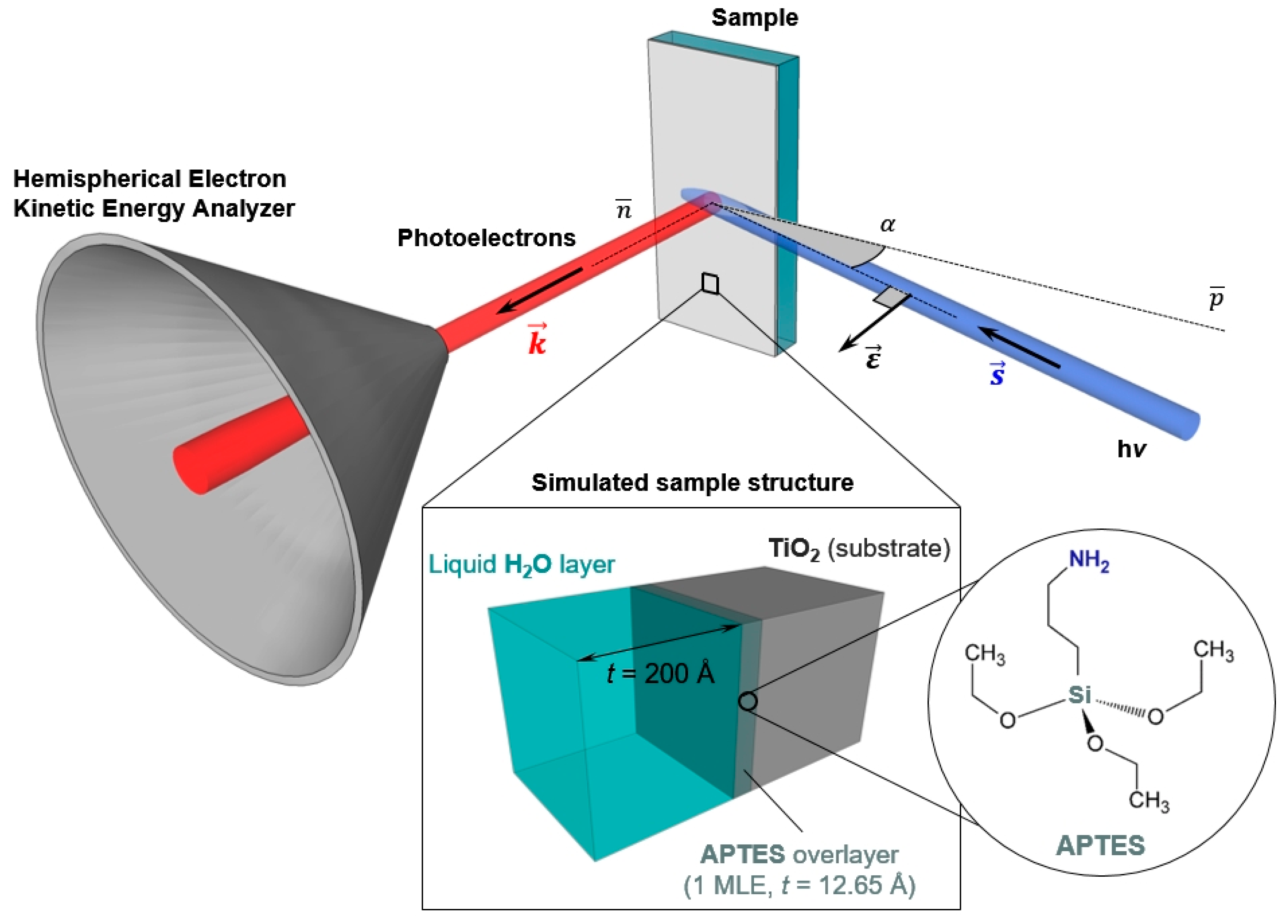
3.2. Optimization of the AP-HAXPES Experimental Conditions
The simulations have been generated using the SESSA software [
22] (see “Materials and Methods” section for the simulation details). Our model system is constituted by a TiO
2 surface functionalized with 1 MLE of APTES, characterized by a thickness of 12.7 Å. To complete our model of the solid/liquid interface, a water layer with a thickness of 20 nm was placed atop the sample surface, as schematically reported in
Figure 1. This value has been taken as a realistic representation of the liquid layer thickness typically obtained during “dip and pull” experiments and accessible by HAXPES [
11,
12,
13,
14,
15,
16,
17].
The use of HAXPES in combination with AP experiments leads to several advantages:
The high photon energy (and correspondingly the photoelectron KE) drastically decreases the secondary electron emission cross sections. This has a beneficial effect in limiting the radiation-induced damage suffered by the sample and the correlated radiolysis of water [
42];
The inelastic scattering between photoelectrons and gas molecules decreases as a result of the large energy difference existing between the X-ray energy and the rotovibrational/electronic excitations and ionization thresholds in the gas molecules (typically falling within the UV-VIS and soft X-ray regions, respectively, for most gases of interest such as O2, N2, H2O, CO, CO2, gaseous hydrocarbons and alcohols);
The elastic scattering between photoelectrons and gas molecules, which is responsible for smearing out the photoelectron angular distribution, is less pronounced due to the generally increasing forward focusing effect as the excitation energy increases [
43];
To maximize the overall photoelectron yield in HAXPES, quasi-normal emission detection is typically coupled with X-ray grazing incidence (α ≤ 5⁰) [
44,
45,
46,
47]. This has the advantage of minimizing the secondary (inelastic) electron background [
46];
The high photoelectron KEs lead to increased photoelectron IMFPs in the liquid and thus enable the investigation of solid/liquid junctions through liquid layers whose thickness is of the same order of the photoelectron information depth.
On the other hand, the large probing depth reduces the relative contribution of the interface region with respect to the overall detection (which includes the bulk liquid and solid signals). In addition, the total photoionization cross sections (TPCSs) decrease with increasing photon energy, thereby further reducing the signal coming from the interface (within our model, the signal coming from the APTES overlayer whose thickness is comparable to typical electrical double layer thickness in solution).
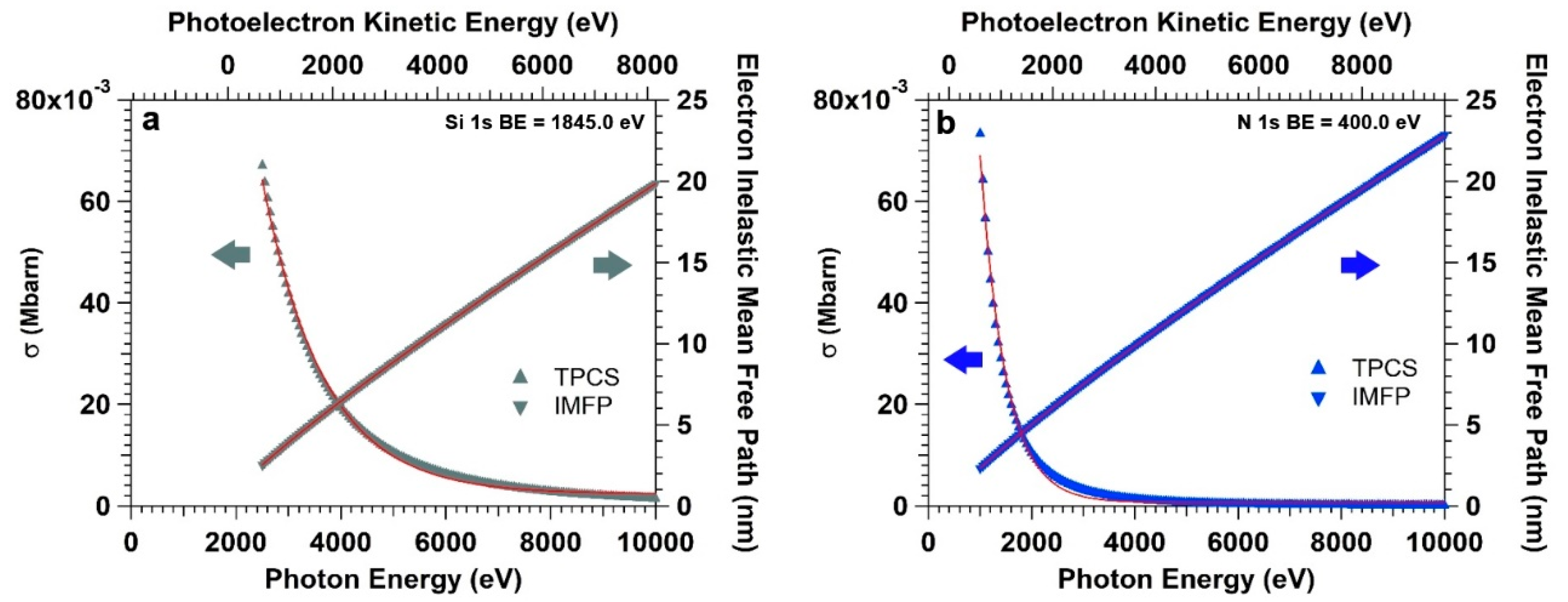
Figure 4a,b clearly illustrate the scenario, reporting the photoelectron IMFP (right axes) and TPCS (left axes) for Si 1s and N 1s core levels (from the APTES overlayer) as a function of photon energy. The IMFP is calculated for photoelectrons traveling in pure water. The IMFP (Λ
e) and TPCS (σ) trends have been fitted using the following relations (Equations (3) and (4), respectively):
C,
p, σ
0 and τ are fitting parameters, whereas hν denotes the photon energy. Note that we have chosen to report the TPCS instead of the differential PCS (DPCS) in order to provide a general discussion about the photon energy dependency of the PCS, since the DPCS strongly depends on the specific experimental geometry and utilized multipole expansion truncation (see “Materials and Methods” section for details). The TPCSs have been determined by interpolation of the TPCS values reported by Yeh and Lindau [
48], whereas the electron IMFPs have been computed using the Tanuma–Powell–Penn (TPP-2M) predictive equation [
49].
Table 2 reports the determined
p, τ and σ
0 values for both analyzed core levels, which will be used later to rationalize the observed behavior of the Si and N 1s core level photoelectron intensity trend as a function of the photon energy.
Therefore, it is necessary to find the optimal photon energy that enables to selectively enhance the signal coming from the interfacial region. In addition, as
Figure 4a,b and
Table 2 show, this evaluation needs to be performed for the different core level spectra involved in the investigation, since they are characterized by different cross sections with different photon energy dependency.
Let us start by quantitatively defining the photoelectron intensity for a given core level characterized by principal and angular quantum numbers
n and
l, respectively. The photoelectron intensity
Inl in vacuum, normalized by the incident X-ray flux integrated over the irradiated sample volume and the analyzer acceptance solid angle over the surface, is given by Equation (5):
ρ(x, y, z) is the number of emitters for unit volume (atomic density),
z is the photoelectron path in the material measured along the surface normal, Λ
e is the IMFP, (dσ/dΩ)
nl is the DPCS, and
θ is the take-off angle formed between the photoelectron propagation direction and the surface normal. We need now to solve the integral reported in Equation (5) for core levels belonging to the interface (in our case, the APTES overlayer) by systematically changing the photon energy, in order to find the energy value that maximizes
Inl. This is given by the trade-off between the increase in the probing depth and the DPCS (TPCS) lowering at increasing photon energies. To this end, we have performed a series of SESSA simulations keeping the detection geometry fixed (α = 15°,
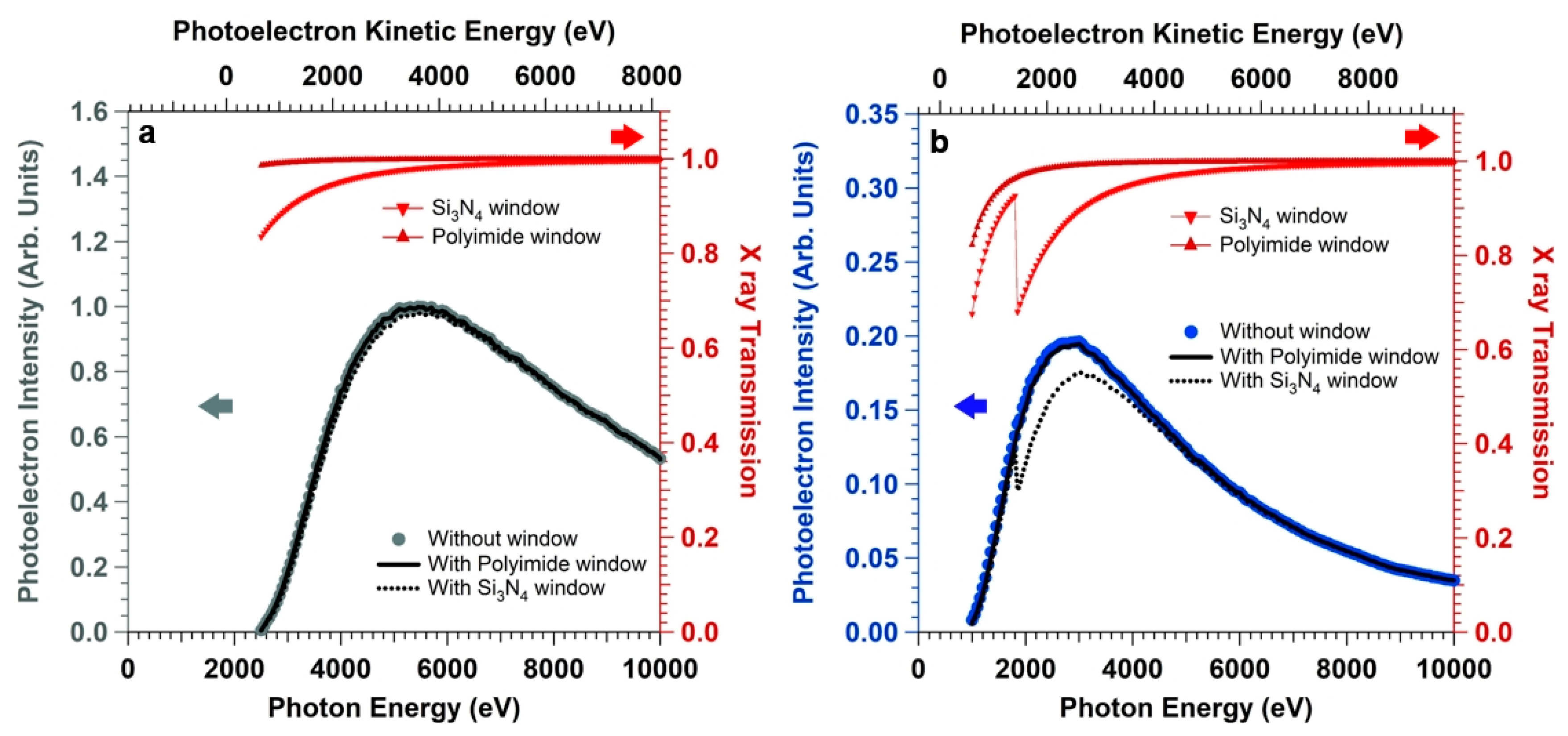
θ = 0°) and varying the photon energy of the incoming radiation (considered as 100% linearly polarized in the orbit (horizontal) plane) with a step of 50 eV. Note that the simulated detection geometry is the same to the one experimentally available at BL 9.3.1, ALS. The results of these simulations are reported in
Figure 5a,b for the Si and N 1s core level photoelectron intensity (left axes), respectively.
The intensity of the Si 1s core level spectrum (BE = 1850 eV) initially increases for photon energy values between 2500 and 4500 eV (
Figure 5a). This is due to the fact that the increasing photoelectron KE leads to an increase of the IMFP, which balances the decay of TPCS (since the photon energy moves away from the Si KLL threshold, centered between 1800 and 1900 eV). As the photon energy further increases, the exponential decay of the TPCS starts to dominate over the other terms in Equation (5), with the intensity curve leveling off and eventually reaching a maximum at a photon energy of 5390 eV (the intensity curve has been fitted using a lognormal function in order to accurately characterized the maximum). At this energy, the TPCS is about e
−2.0 the value at 2500 eV (σ
0 = 0.062 Mbarn), whereas the probed depth (defined as the depth from which 95% of the emitted electrons are inelastically scattered, i.e., 3∙λ
e) is about 40 nm (that is two times the thickness of the water layer). For higher energies, the TPCS dominates and a monotone decrease of the photoelectron intensity can be observed in line with the exponential decay of the TPCS. The intensity trend of the N 1s core level spectrum as a function of the photon energy (
Figure 5b) follows a similar qualitative trend, however shifted in photon energy (photoelectron KE) due to the lower energy threshold of the KLL transition (at around 400 eV). The maximum of the intensity curve is reached at a photon energy of about 2850 eV, for which the TPCS is equal to about e
−3.0 the value at 1000 eV (σ
0 = 0.071 Mbarn). The information depth at 2890 eV is equal to about 25 nm.
We can therefore rationalize the observed dependencies drawing some general conclusions:
For core levels whose electronic excitation energies (and therefore BEs) fall within the soft X-ray region (below 1000 eV), the TPCS decreases rapidly as the photon energy increases within the hard X-ray region (above 2000 eV). For core levels characterized by higher electronic excitation energies (approaching or within the hard X-ray region), the corresponding TPCS decreases with a lower rate with the increase of the photon energy;
The IMFP follows the same functional dependency with the photon energy for both type of core levels;
The combination of the two aforementioned points lead to the following phenomenology: the maximum of the photoelectron intensity of different core levels belonging to the interface region lies at different photon energies. For soft X-ray core levels, the trade-off between relatively high KEs and the fast decay of TPCS leads to probed depths at the curve maximum essentially matching the electrolyte overlayer thickness. For hard X-ray core levels, instead, the slower decay of the TPCS with the photon energy leads to information depth at the maximum of the photoelectron intensity curve higher than the water overlayer thickness. In addition, the intensity curve for hard X-ray core levels is characterized by a broader spectral range compared to that for soft X-ray spectra. In our case, the full-width at half-maximum (FWHM) of the Si 1s intensity curve is about 6500 eV, whereas the same for the N 1s core level is characterized by a FWHM of about 4150 eV.
Furthermore, we simulated the effect of introducing an X-ray absorber between the X-ray source and the sample, which is typically done in order to seal the X-ray source (beamline or anode source) from the high pressure environment.
Figure 5 reports the X-ray transmission (right axes) through a 500 nm-thick Si
3N
4 and Kapton window (the calculations of the X-ray transmission as a function of the photon energy (1000 eV–10000 eV) and fixed incidence angle α at the window (α = 90°) have been performed using the database of the Center for X-ray Optics (CXRO) of the Lawrence Berkeley National Laboratory (Berkeley, U.S.A) [
50]). We can observe that working with hard X-rays (photon energy above 2000 eV) and Kapton windows keeps the X-ray transmission close to unity even for relatively thick windows (X-ray transmission above 95 %). On the other hand, for Si
3N
4 windows the Si KLL absorption edge between 1800 and 1900 eV decreases the transmission above 2000 eV (by about 30%, 20%, and 10% at a photon energy of 2000, 2500, and 3100 eV, respectively). The Si and N 1s photoelectron intensities have been then convoluted with the simulated X-ray transmission. We can observe that the Si 1s intensity trend (
Figure 5a) is basically not influenced by the presence of the window (either Si
3N
4 or Kapton), with an intensity decrease at the maximum (hv = 5390 eV) of about 2% in the case of a Si
3N
4 absorber. On the other hand, for the soft X-ray N 1s core level (
Figure 5b), the presence of the Si
3N
4 window leads to an appreciable loss of the photoelectron intensity at the curve maximum (by about 15 % compared to the simulation performed without absorber). Moreover, the maximum of the intensity curve is blue-shifted (~250 eV) by the presence of the Si
3N
4 window compared to the curve obtained with no absorber. In line with the findings obtained for the Si 1s core level intensity curve, the presence of the 500 nm-thick Kapton window does not induce a shift of the N 1s core level intensity curve, with a loss of signal at the maximum less than 2% compared to the calculation performed without absorber. We want to highlight that the presence of a differentially-pumped aperture (pin-hole) instead of an X-ray window will lead to the same results obtained for no X-ray absorber, since the former implies a simple photon energy-constant lowering of the photon flux at the sample.
Overall, this analysis elucidates the importance of tuning the photon energy for different core levels belonging to the interface region buried by a nanometric-thick electrolyte layer, in order to keep the optimal core level “brightness” and enhance the investigation of the solid/liquid interface. Moreover, it shows that another important parameter to keep in mind for enhancing the photoelectron intensity is the choice of the X-ray window, in particular for soft X-ray core levels.
3.3. Evolution of the Physical/Chemical Properties of the Solid/Liquid Interface as a Function of the Electrolyte pH
In this section, we will show a practical example of the potentials offered by coupling the “dip and pull” method with AP-HAXPES. We investigated a sol-gel spin-coated TiO
2 surface functionalized with ~1 MLE of APTES, using a fixed photon energy of 4000 eV. This value is close to the average (4120 eV) of the two energies retrieved above to enhance the signal intensity from Si and N 1s core levels within the APTES overlayer. In addition, the photon flux at the sample at photon energies of 2850 eV and 5390 eV at BL 9.3.1 at the Advanced Light Source was not optimal due to experimental limitations of the beamline optics. We studied the solid/liquid interface formation by investigating the surface in its pristine conditions (high vacuum, HV, about 10
−6 mbar) (i), by exposing it to ~70% RH at room temperature (hydrated conditions, HC) (ii), and finally after dipping the surface in pure water and different aqueous electrolytes (iii), changing the pH from 7 to 14 (see also
Table 1). The dipping was performed in about 70% RH environment at room temperature (p
water ~ 21 mbar).
It is important to note that the experimental BE values measured in this work for light elements such as O and N are slightly higher than those reported in the literature for similar systems. This might be due to recoil effects when momentum is transferred from the ejected photoelectron to the emitting atom. Recoil is present in all photoemission processes and its effects are non-negligible for high photoelectron KEs and light elements [
51,
52]. At a photon energy of 4000 eV the calibration performed on gold using the Au 4f
7/2 core level signal (KE ~ 3916 eV) is essentially not influenced by the recoil (the corresponding loss is about 10 meV). On the other hand, the energy loss for the O 1s (KE ~ 3470 eV) core level spectrum is about 120 meV.
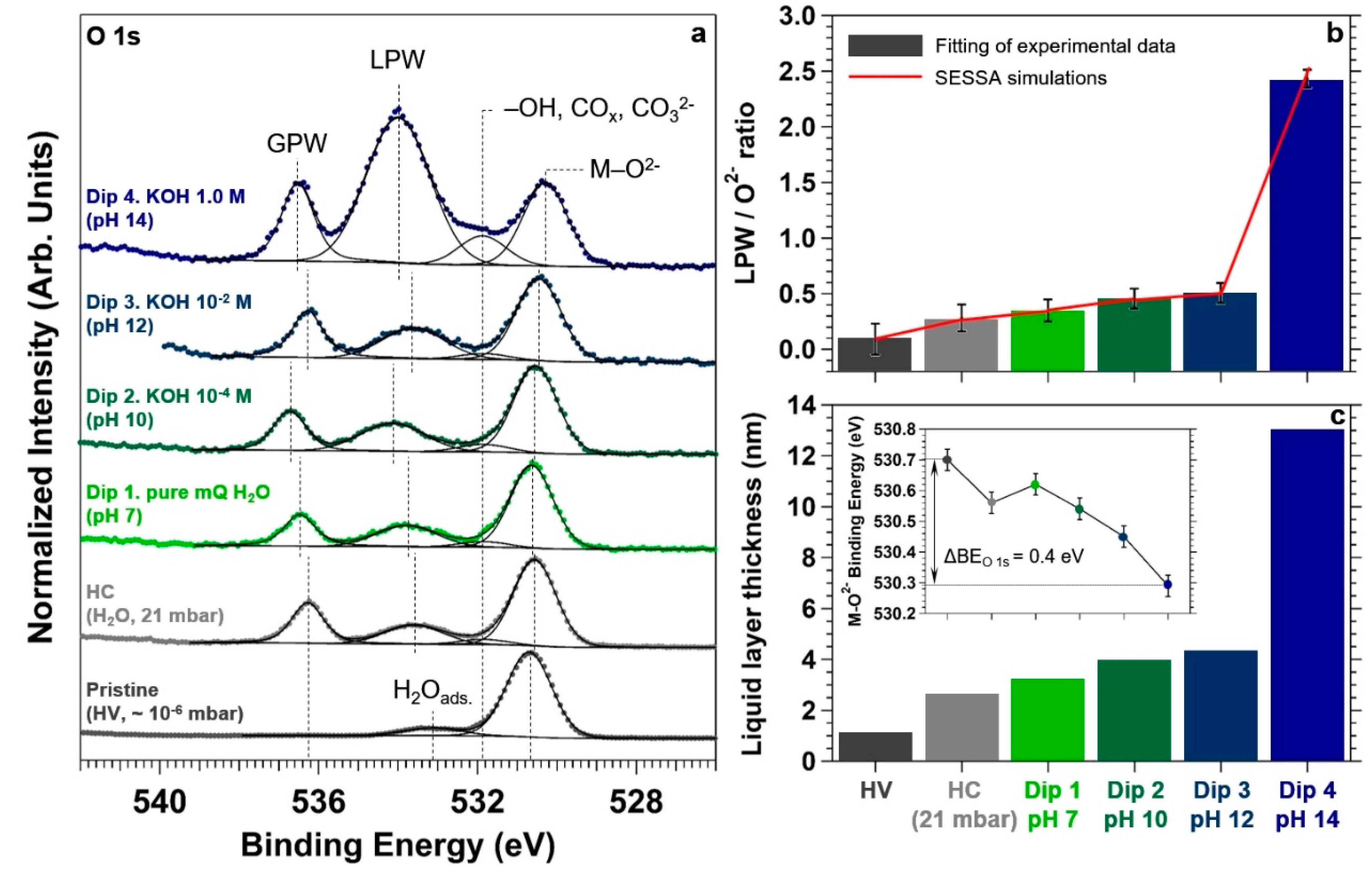
To monitor the formation of the liquid electrolyte layer on the surface, we acquired the O 1s core level spectrum at all the aforementioned conditions, as reported in
Figure 6a. At pristine conditions, the O 1s spectrum exhibits an intense peak centered at a BE of about 530.7 eV, attributable to the TiO
2 lattice oxygen (O
2−) [
53,
54]. A minor component can be observed at about 533.1 eV, most likely due to molecularly adsorbed water (H
2O
ads.) on Ti
4+ sites [
53] and on the APTES terminal –NH
2 groups upon exposure to air [
55]. It is in fact suggested by Meroni et al. in a recent work that APTES chemisorption on TiO
2 mainly occurs through the formation of one or two Si−O−Ti bonds involving the Si headgroup [
56], whereas adsorption via the terminal amino group seems instead considerably more labile. Therefore, the Lewis base-character of the amine group might induce water adsorption at the nitrogen atom through hydrogen bond formation with water molecules.
At HC and for the dipping experiments in the different aqueous electrolytes, we can observe the presence of two new spectral features in the O 1s core level spectrum. The first, centered at a BE between 533.6 and 534.0 eV is attributable to liquid phase water (LPW) due to the formation of the liquid layer, whereas the second peak is associated to the gas phase water (GPW) (in the BE range of 536.3 and 536.6 eV) [
53]. The shift in BE of these two components is typically associated to work function changes at the sample surface [
57] due to the different explored conditions.
In addition, passing from the pristine conditions to HC and for the dipping experiments in the different aqueous electrolytes, it is possible to observe the development of a third feature centered at a BE of about 531.8 eV. The origin of such a spectral component, under the particular conditions of the experiment, is not trivial and it can be due to a number of different causes. First, the observed BE is typical of surface hydroxyl groups generated from the well-known dissociative adsorption of water for pressures above ~ 10
−3 mbar [
53]. Second, oxygen-containing carbon compounds from background contamination can also produce a peak at this BE, particularly after filling the chamber with water vapor for several minutes at relatively high pressures. The contamination originates most likely from environmental CO
2 and hydrocarbons containing CO
x groups. This is typically caused by the displacement of molecules from the chamber walls upon exposure to water vapor at or above the mbar pressure range or from molecules contained in the water vapor source itself [
53]. Third, the formation of non-volatile carbonates during the preparation of the alkaline electrolytes in ambient conditions (CO
2 + 2 KOH → K
2CO
3 + H
2O) can lead to the “deposition” of carbonates on the sample surface during the “dip and pull” procedure. The reported BE for carbonate groups (531.9 eV [
58]) is also consistent with our findings. The “deposition” of carbonates at the highest investigated pH might be the main cause of the important intensity increase of the spectral component observed when passing from pH 12 to pH 14.
We want now to focus the reader’s attention on the photoelectron intensity evolution of the LPW component during the experiment.
Figure 6b,c report the LPW to O
2− ratio and the corresponding water layer thickness estimation, respectively. To do so, SESSA simulations have been performed using the same sample structure reported in
Figure 1. By changing the water overlayer thickness, the simulated LPW/O
2− ratio was adjusted to match the experimentally-determined value for each condition. Passing from the first dipping in pure water to the third in KOH 10
−2 M (pH 12), the LPW/O
2− ratio changes from about 0.3 to 0.5, which corresponds to an electrolyte layer thickness between 3 and 4 nm. Within the experimental uncertainty, these are similar thicknesses found at HC, after exposing the sample to about 21 mbar of water (~ 2.5 nm). This means that a thin layer of water condensed on the surface at HC (~ 70% RH), and that the thickness of the liquid layer did not depend on the successive dipping procedures in pure water (pH 7) and in KOH 10
−4 and 10
−2 M aqueous solutions (pH 10 and 12, respectively). Differently, at pH 14 (KOH 1.0 M) the LPW/O
2− ratio increases up to ~2.5 (
Figure 6b), which corresponds to an electrolyte layer thickness of about 13 nm (
Figure 6c).
To find the reason for the observed phenomenology, we use the Henderson–Hasselbalch equation to estimate the ratio between the unprotonated (–NH
2) and protonated (–NH
3+) amine groups as a function of the electrolyte pH (–NH
2/–NH
3+ = 10
pH-pKa). This procedure allows us to qualitatively assess the net charge at the surface under the different explored conditions, thereby inferring about the interaction between the functionalized charged surface and the liquid water. Using a value of the APTES amine group acid dissociation constant (pKa) of 10.6 as reported by Notsu et al. [
59], we find a –NH
2/–NH
3+ ratio of 2.5 ∙ 10
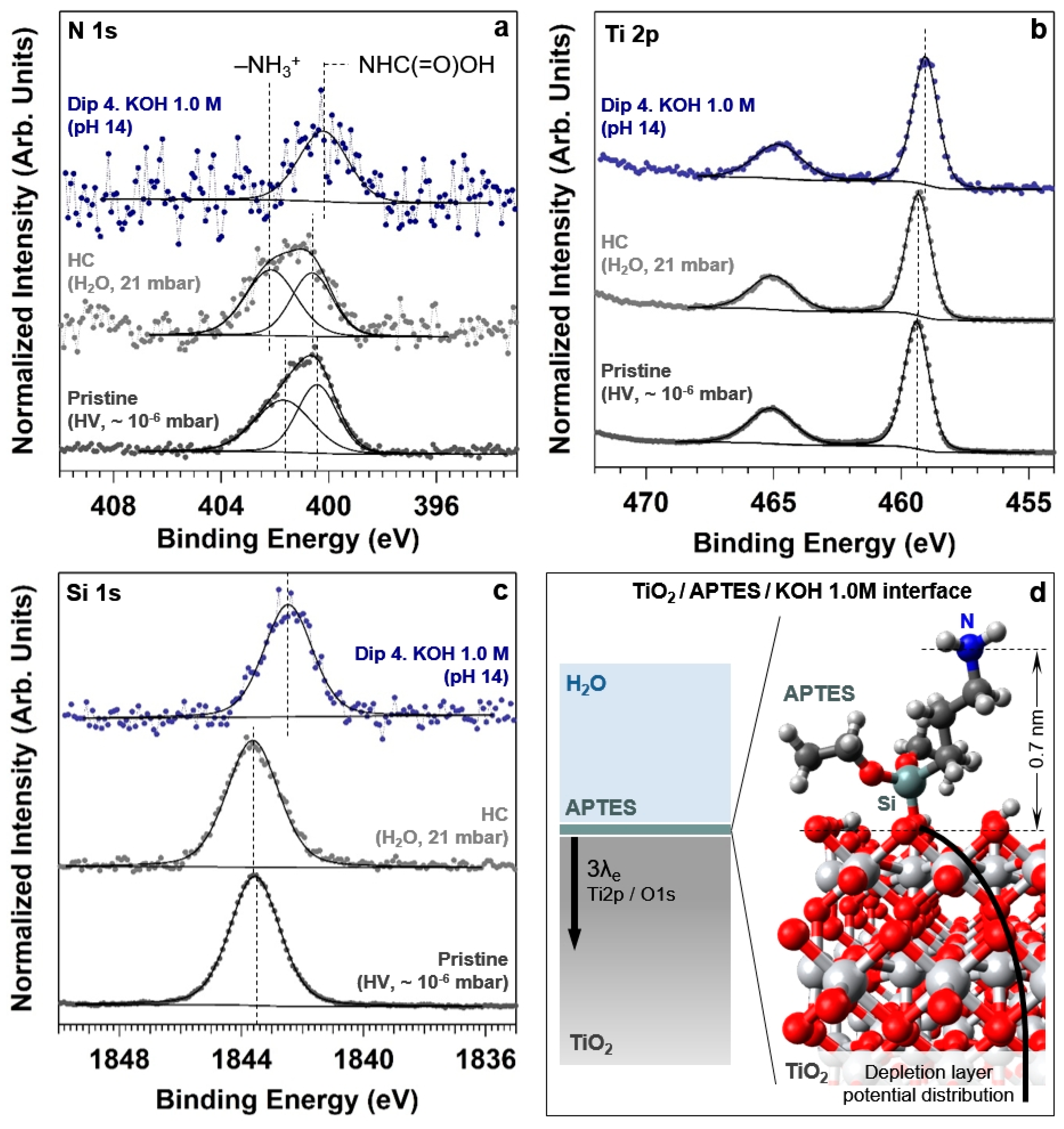
−4, 0.25, 25, and 2500 at pH 7, 10, 12, and 14, respectively. This means that for pH values below (above) the pKa, the amine group is present on the surface mainly in its protonated (unprotonated) form. This is qualitatively demonstrated by the N 1s core level spectra reported in
Figure 7a for the pristine conditions, hydrated conditions and after dipping the sample in the KOH 1.0 M solution (pH 14). The spectrum acquired on the pristine surface exhibits a clear asymmetry toward high BEs, and can be fitted using two spectral components centered at a BE of 400.4 and 401.7 eV (with a FWHM of 1.8 and 2.4 eV, respectively). Taking into account a positive 140 meV shift of the BE due to the recoil loss, the identified BEs for these components are in line with previous studies [
56] and can be associated with carbamate (–NHC(=O)OH) and –NH
3+ moieties present at the APTES overlayer, respectively. Interestingly, within the detection limit of the technique (about 1 at.%), we do not observe the presence of unprotonated amine groups (which should generate a peak at a BE of 399.6 eV [
56]). This might be due to the fact that the –NH
2 groups readily reacted with environmental CO
2 to form carbamates upon exposing the sample to ambient conditions, after the APTES functionalization of the TiO
2 surface [
60]. Exposing the sample to ~ 70% RH at room temperature leads to an increase of the –NH
3+ surface concentration (in agreement with the Henderson–Hasselbalch equation for pH 7), accompanied by an upward BE shift of both spectral components (by about 0.3 eV). After dipping the sample in the KOH 1.0 M solution (pH 14), it is possible to observe the disappearance of the protonated amine component as predicted by the Henderson–Hasselbalch equation. Under these conditions, the N 1s core level peak could be fitted using only one spectral component, characterized by a FWHM of 2.2 eV and centered at a BE of about 400.0 eV. This value is about 0.4 eV lower than the BE reported above for the carbamate moieties present on the pristine surface (400.4 eV). We will give a plausible explanation for such a shift later at the end of this section.
We can then conclude that for pH values below the –NH
2 pKa (7 and 10), the presence of the protonated amine groups, although positively charged, prevents the formation of a stable and relatively thick water layer leading to the observed partial non-wetting behavior. Above the –NH
2 pKa (pH 12 and 14), no protonated –NH
3+ groups are essentially present on the surface, while the majority of the free (unprotonated) amine groups are converted into carbamate moieties by the nucleophilic CO
2 or CO
32− attack (keep in mind that the O 1s revealed an enhanced CO
32− photoelectron signal at pH 14, most likely due to the high availability within the liquid layer of non-volatile carbonates formed during the preparation of the solution). In this case, the absence of formal charges at the surface might weaken its interaction with water. On the other hand, at pH 14 we observe a different behavior, in which the surface shows a higher hydrophilicity character. It is reported that the surface hydroxy groups on TiO
2 possess acidic character [
61] and can therefore easily donate H (Brønsted acid) in strong alkaline conditions [
61,
62]. Therefore, the deprotonation reaction occurring at the solid/liquid interface (–OH + H
2O → –O
– + H
3O
+) at pH 14 generates a surface negative charge that might be responsible for the stabilization of a thicker liquid layer compared to those observed at lower pH values.
The development of a negative surface charge driven by the pH increase leads also to a second effect. In
Figure 6a it is possible to qualitatively observe a negative BE shift of the O
2− component. The inset reported in
Figure 6c shows the O
2− BE trend as a function of the different explored conditions. The downward BE shift is equal to 0.4 eV passing from pristine conditions to the final dip in pH 14, and it is attributable to an upward band-bending in TiO
2 (formation of a depletion layer at the solid/liquid interface). This is confirmed by the observation of the same negative BE shift when acquiring the Ti 2p core level spectrum, as reported in
Figure 7b for the same experimental conditions. Passing from pristine to pH 14 conditions, the BE measured on the Ti 2p
3/2 spectrum is equal to 459.3 and 458.9 eV, respectively. The observed negative 0.4 eV shift is thus in agreement with the previous findings. It is worth noting that the photoelectrons generated from the ionization of the O 1s and Ti 2p
3/2 core levels have similar KEs (the difference being about 70 eV), which leads to the same information depth at a photon energy of 4000 eV (~17 nm). This means that the information carried by the BE shift is generated by the spectral summation within the depletion layer, convoluted with the exponential decay of the photoelectron intensity. In addition, we want to highlight that no appreciable FWHM change is observed on the lattice oxygen spectral component or in the Ti 2p
3/2 spectrum, passing from pristine conditions to pH 14. This might be due to the difference between the information depth (using O 1s and Ti 2p
3/2 core levels) and the thickness of the space charge region (SCR). Using a concentration of donors of 1 × 10
18 cm
−3 for intrinsic
n-doped TiO
2 [
63] and a band bending potential of 0.4 V as determined experimentally (assuming flat bands at the pristine conditions), the space charge region thickness can be estimated to be about 45 nm [
64].
We can make use of the adsorption of the APTES molecules at the TiO
2 top-most layer to probe the electrical potential value at the upper part of the band-bending potential distribution, by using a core level spectrum from an element belonging to the APTES overlayer (e.g., Si and N 1s). In the case of the Si 1s spectrum (
Figure 7c), the negative BE shift between the pristine and the pH 14 conditions is considerably larger than that observed for O 1s and Ti 2p
3/2, being equal to ~1.1 eV. This value represents therefore the maximum band bending in the depletion layer of TiO
2.
On the other hand, as already introduced above, for the N 1s core level spectrum we observe a negative shift of the carbamate group BE of about 0.4 eV, passing from pristine to pH 14 conditions. This could be generated by two causes. First, the nitrogen atom is not “directly” adsorbed at the TiO
2 top-most layer, differently than the silicon atom, but it is screened by three alkyl units from the latter. Therefore, the presence of four single covalent bonds (Si–C, C–C, C–C and C–N) between the silicon and the nitrogen atom might lower the potential experienced in the latter. Second, as schematically reported in
Figure 7d, the nitrogen atom is dangling from the surface into the liquid layer, thereby experiencing the electrical potential drop in solution. The Debye length k
−1 for a monovalent ion in an aqueous solution at room temperature is related to the concentration C of the electrolyte by k
−1 = 3.04 × C
−1/2 (C is expressed in mol L
−1, or M, and k in Å). This means that for a 1.0 M solution, the Debye length is equal to about 0.3 nm. Defining the thickness of the Gouy–Chapman diffuse layer as three times the Debye length (i.e., at which distance the potential at the sample surface is ∼95% screened in solution), we find that such a thickness is equal to 0.9 nm. We performed a molecular dynamics simulation of the adsorption of one APTES molecule on a rutile TiO
2(110) surface through the formation of one Ti–O–Si bond (
Figure 7d). To further confirm this, we used an UFF force field and a convergence cut off of 10
−6. The simulated distance between the nitrogen and the ideal plane containing the-top most layer oxygen atoms is equal to about 0.7 nm, which is similar to the thickness of the diffuse layer calculated above. This means that the nitrogen atom might experience the local potential at the slip plane (that is, at the ideal plane between the diffuse layer and the bulk solution). The two described effects might then account for the different BE shift measured on the N 1s core level spectra with respect to the value measured using the Si 1s core level.

 ,
, 


