Preparation of V2O5 Thin Film by Sol–Gel Technique and Pen Plotter Printing

 , , , and
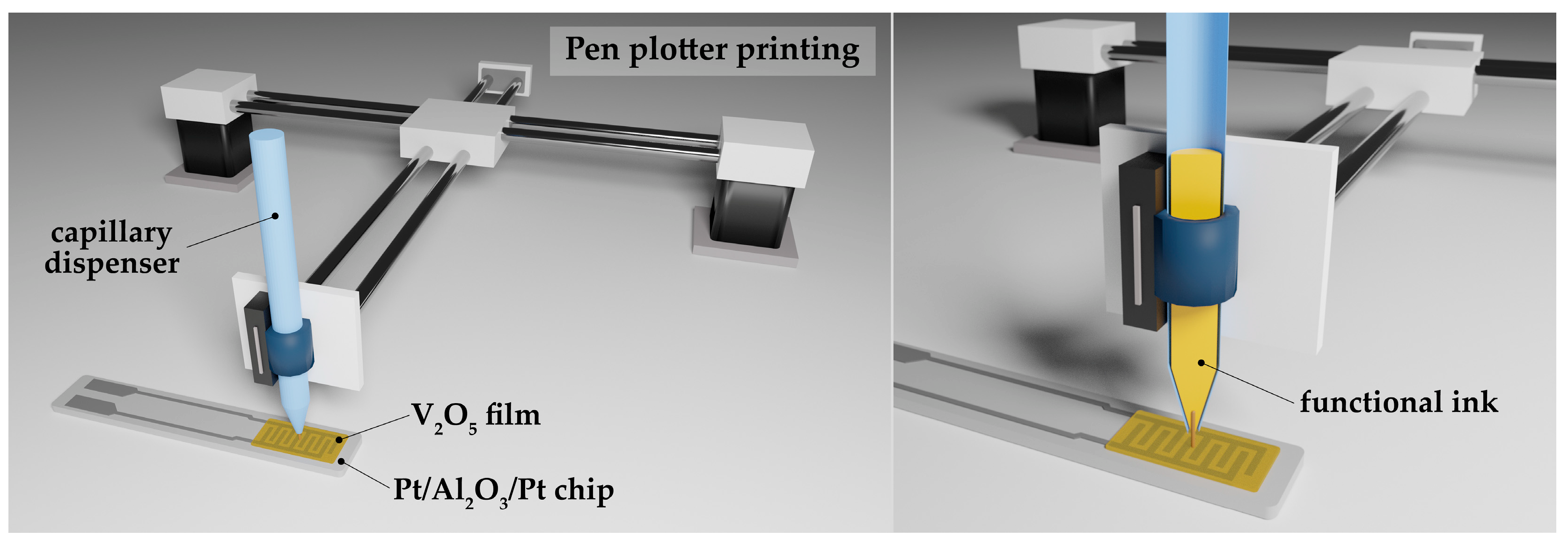
Abstract
:1. Introduction
2. Materials and Methods
2.1. Materials
2.2. Hydrolytically Active Precursor Synthesis
2.3. Pen Plotter Printing of Oxide Films
2.4. Instrumentation
3. Results and Discussion
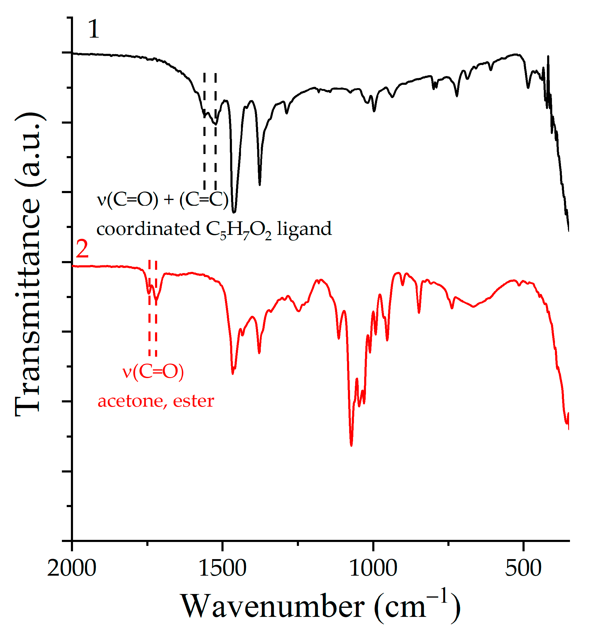
3.1. Precursor Synthesis and Characterization
x CH3C(O)OC4H9
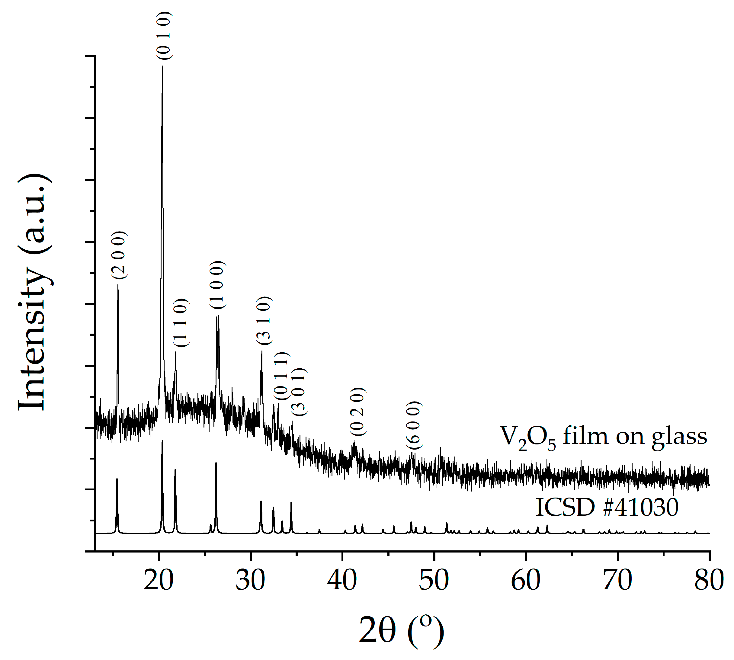
3.2. V2O5 Thin Film Crystal Structure
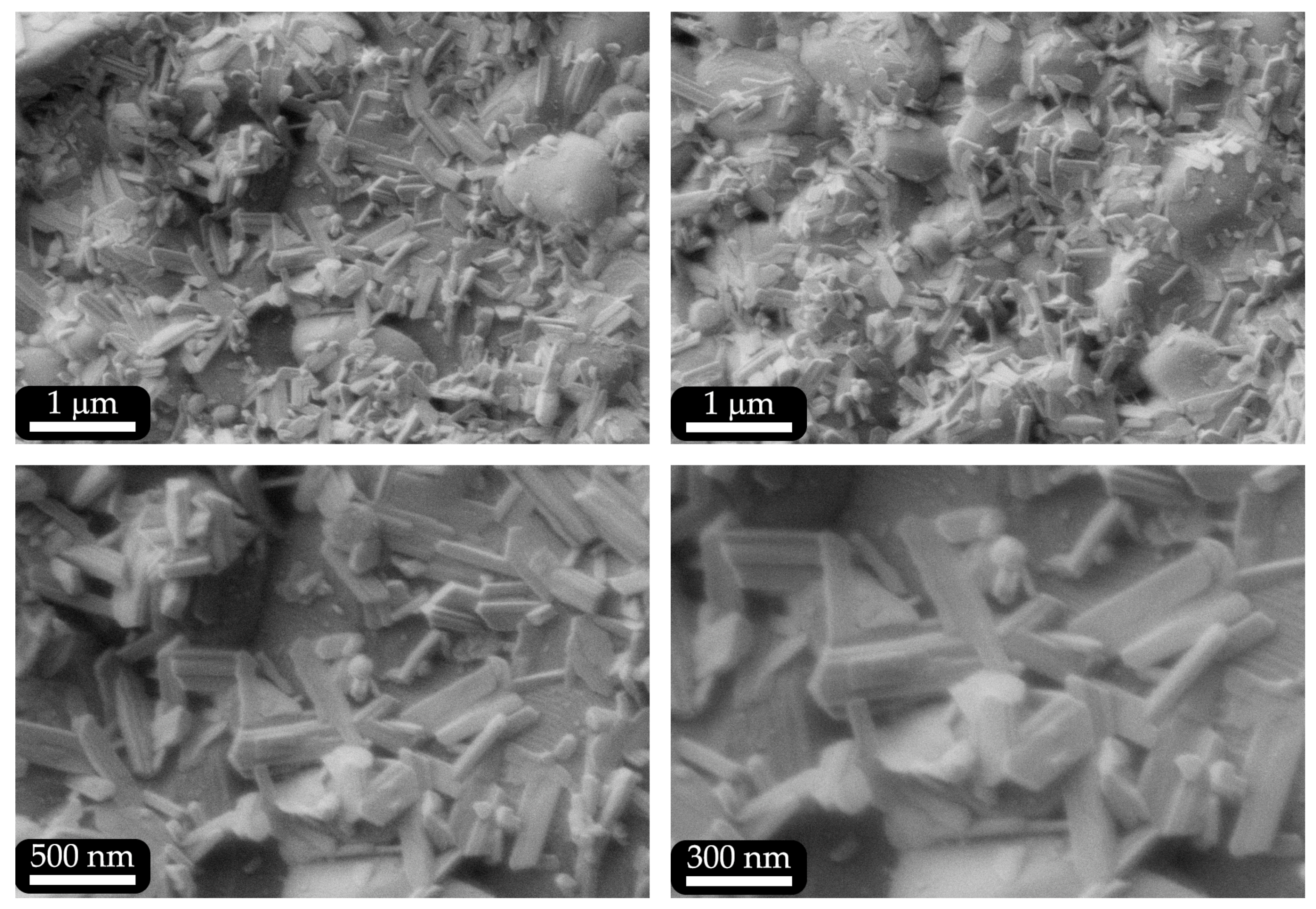
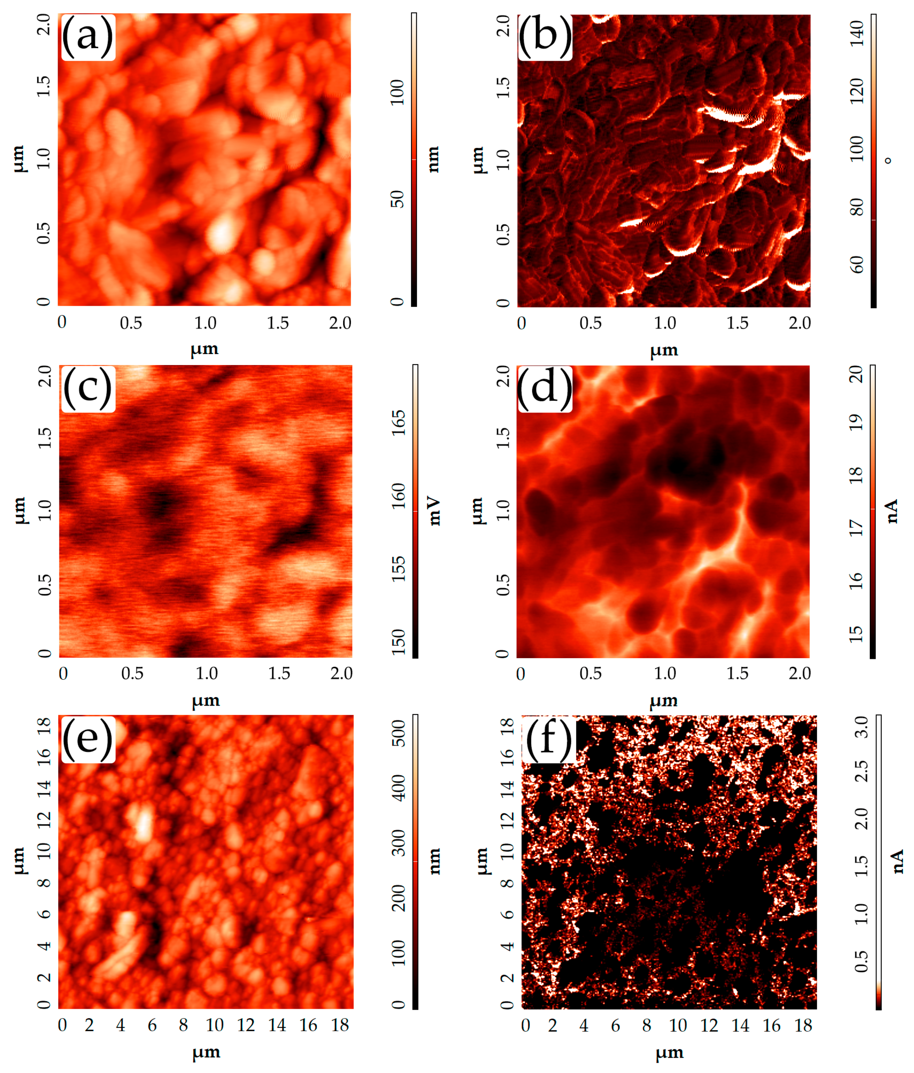
3.3. Oxide Film Microstructure
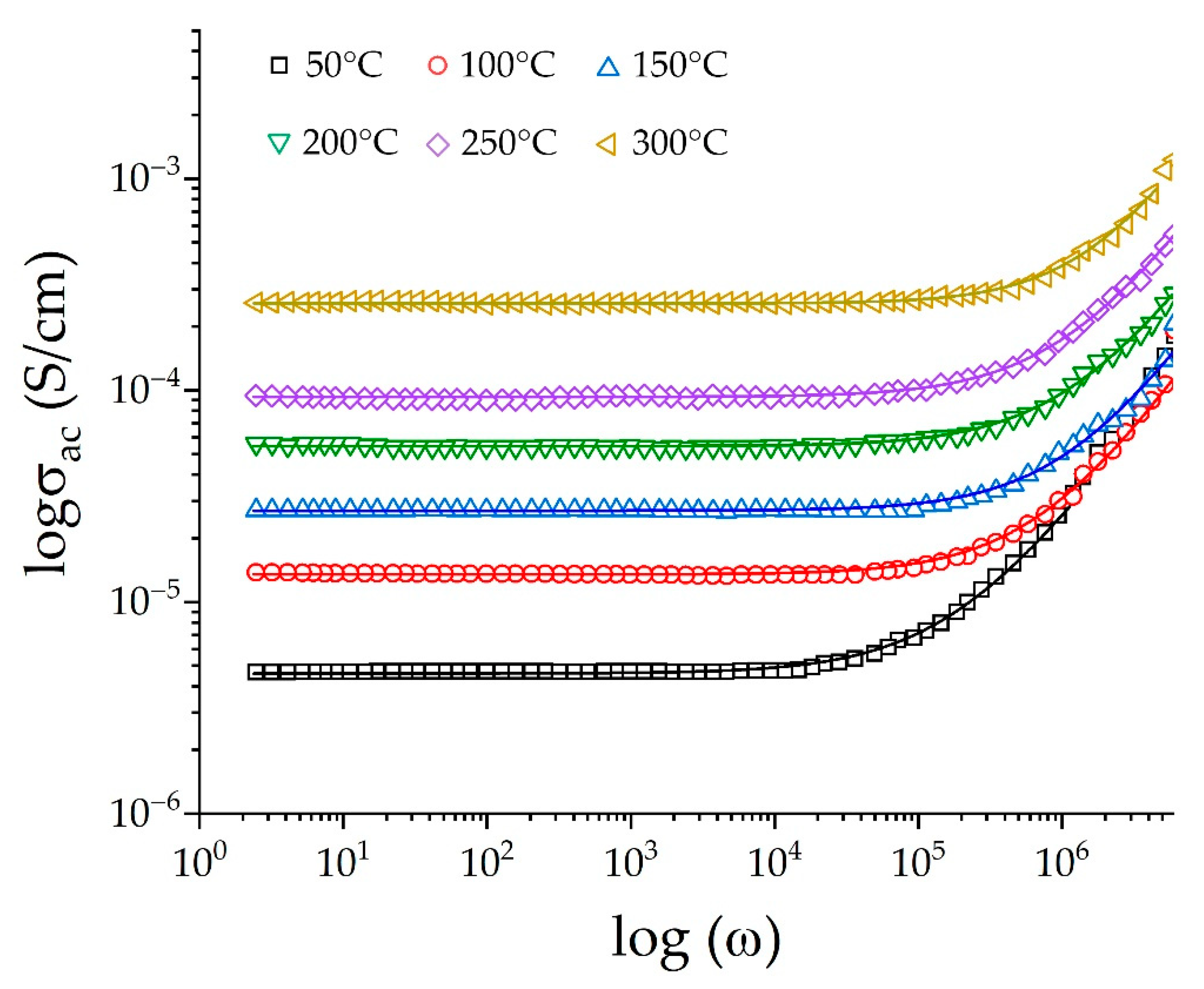
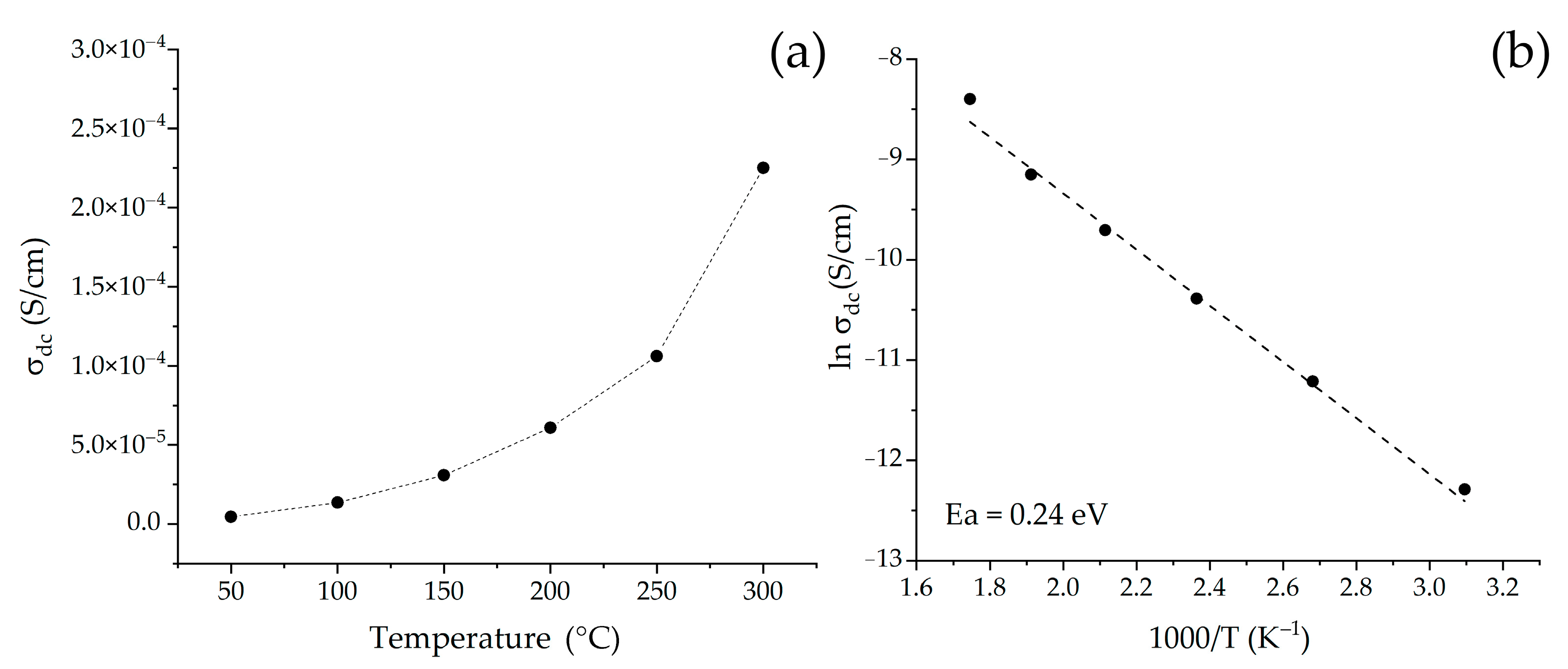
3.4. Electrophysical Properties of Prepared V2O5 Film
4. Conclusions
Author Contributions
Funding
Institutional Review Board Statement
Informed Consent Statement
Data Availability Statement
Conflicts of Interest
References
- Cheng, K.C.; Chen, F.R.; Kai, J.J. V2O5 Nanowires as a Functional Material for Electrochromic Device. Sol. Energy Mater. Sol. Cells 2006, 90, 1156–1165. [Google Scholar] [CrossRef]
- Wang, Y.; Cao, G. Li+-Intercalation Electrochemical/Electrochromic Properties of Vanadium Pentoxide Films by Sol Electrophoretic Deposition. Electrochim. Acta 2006, 51, 4865–4872. [Google Scholar] [CrossRef]
- Ramana, C.V.; Smith, R.J.; Hussain, O.M.; Chusuei, C.C.; Julien, C.M. Correlation between Growth Conditions, Microstructure, and Optical Properties in Pulsed-Laser-Deposited V2O5 Thin Films. Chem. Mater. 2005, 17, 1213–1219. [Google Scholar] [CrossRef]
- Jin, A.; Chen, W.; Zhu, Q.; Jian, Z. Multi-Electrochromism Behavior and Electrochromic Mechanism of Electrodeposited Molybdenum Doped Vanadium Pentoxide Films. Electrochim. Acta 2010, 55, 6408–6414. [Google Scholar] [CrossRef]
- Zanarini, S.; di Lupo, F.; Bedini, A.; Vankova, S.; Garino, N.; Francia, C.; Bodoardo, S. Three-Colored Electrochromic Lithiated Vanadium Oxides: The Role of Surface Superoxides in the Electro-Generation of the Red State. J. Mater. Chem. C Mater. 2014, 2, 8854–8857. [Google Scholar] [CrossRef]
- Wang, S.; Li, S.; Sun, Y.; Feng, X.; Chen, C. Three-Dimensional Porous V2O5 Cathode with Ultra High Rate Capability. Energy Environ. Sci. 2011, 4, 2854–2857. [Google Scholar] [CrossRef]
- Liu, Y.; Clark, M.; Zhang, Q.; Yu, D.; Liu, D.; Liu, J.; Cao, G. V2O5 Nano-Electrodes with High Power and Energy Densities for Thin Film Li-Ion Batteries. Adv. Energy Mater. 2011, 1, 194–202. [Google Scholar] [CrossRef]
- Narayanan, R. Single Step Hydrothermal Synthesis of Carbon Nanodot Decorated V2O5 Nanobelts as Hybrid Conducting Material for Supercapacitor Application. J. Solid State Chem. 2017, 253, 103–112. [Google Scholar] [CrossRef]
- Jeyalakshmi, K.; Vijayakumar, S.; Nagamuthu, S.; Muralidharan, G. Effect of Annealing Temperature on the Supercapacitor Behaviour of β-V2O5 Thin Films. Mater. Res. Bull. 2013, 48, 760–766. [Google Scholar] [CrossRef]
- De Freitas Neto, D.B.; Parmar, R.; Matsubara, E.Y.; Minicucci, M.; Gunnella, R.; Rosolen, J.M. Nanostructured V2O5.NH2O/Cup-Stacked Carbon Nanotube Composite with Remarkable Li+ Specific Capacity. Solid State Ion. 2021, 363, 115590. [Google Scholar] [CrossRef]
- Zhang, L.; Jiang, C.; Wu, C.; Ju, H.; Jiang, G.; Liu, W.; Zhu, C.; Chen, T. V2O5 as Hole Transporting Material for Efficient All Inorganic Sb2S3 Solar Cells. ACS Appl. Mater. Interfaces 2018, 10, 27098–27105. [Google Scholar] [CrossRef]
- Zilberberg, K.; Trost, S.; Schmidt, H.; Riedl, T. Solution Processed Vanadium Pentoxide as Charge Extraction Layer for Organic Solar Cells. Adv. Energy Mater. 2011, 1, 377–381. [Google Scholar] [CrossRef]
- Wang, D.; Elumalai, N.K.; Mahmud, M.A.; Wright, M.; Upama, M.B.; Chan, K.H.; Xu, C.; Haque, F.; Conibeer, G.; Uddin, A. V2O5 -PEDOT: PSS Bilayer as Hole Transport Layer for Highly Efficient and Stable Perovskite Solar Cells. Org. Electron. 2018, 53, 66–73. [Google Scholar] [CrossRef]
- Choi, S.G.; Seok, H.J.; Rhee, S.; Hahm, D.; Bae, W.K.; Kim, H.K. Magnetron-Sputtered Amorphous V2O5 Hole Injection Layer for High Performance Quantum Dot Light-Emitting Diode. J. Alloys Compd. 2021, 878, 160303. [Google Scholar] [CrossRef]
- Mane, A.A.; Suryawanshi, M.P.; Kim, J.H.; Moholkar, A.V. Fast Response of Sprayed Vanadium Pentoxide (V2O5) Nanorods towards Nitrogen Dioxide (NO2) Gas Detection. Appl. Surf. Sci. 2017, 403, 540–550. [Google Scholar] [CrossRef]
- Huotari, J.; Bjorklund, R.; Lappalainen, J.; Lloyd Spetz, A. Pulsed Laser Deposited Nanostructured Vanadium Oxide Thin Films Characterized as Ammonia Sensors. Sens. Actuators B Chem. 2015, 217, 22–29. [Google Scholar] [CrossRef]
- Wang, D.; Gu, K.; Zhao, Q.; Zhai, C.; Yang, T.; Lu, Q.; Zhang, J.; Zhang, M. Synthesis and Trimethylamine Sensing Properties of Spherical V2O5 Hierarchical Structures. New J. Chem. 2018, 42, 14188–14193. [Google Scholar] [CrossRef]
- Jin, W.; Yan, S.; An, L.; Chen, W.; Yang, S.; Zhao, C.; Dai, Y. Enhancement of Ethanol Gas Sensing Response Based on Ordered V2O5 Nanowire Microyarns. Sens. Actuators B Chem. 2015, 206, 284–290. [Google Scholar] [CrossRef]
- Vijayakumar, Y.; Mani, G.K.; Ponnusamy, D.; Shankar, P.; Kulandaisamy, A.J.; Tsuchiya, K.; Rayappan, J.B.B.; Reddy, M.V.R. V2O5 Nanofibers: Potential Contestant for High Performance Xylene Sensor. J. Alloys Compd. 2018, 731, 805–812. [Google Scholar] [CrossRef]
- Nandakumar, N.K.; Seebauer, E.G. Low Temperature Chemical Vapor Deposition of Nanocrystalline V2O5 Thin Films. Thin Solid Film. 2011, 519, 3663–3668. [Google Scholar] [CrossRef]
- Drosos, C.; Jia, C.; Mathew, S.; Palgrave, R.G.; Moss, B.; Kafizas, A.; Vernardou, D. Aerosol-Assisted Chemical Vapor Deposition of V2O5 Cathodes with High Rate Capabilities for Magnesium-Ion Batteries. J. Power Sources 2018, 384, 355–359. [Google Scholar] [CrossRef]
- Hu, B.; Cheng, H.; Huang, C.; Aslam, M.K.; Liu, L.; Xu, C.; Chen, P.; Yu, D.; Chen, C. The Controlled Study of Surfactants on the Morphologies of Three-Dimensional Turbine-like V2O5 for the Application of High Performance Lithium Ion Storage. Solid State Ion. 2019, 342, 115059. [Google Scholar] [CrossRef]
- Margoni, M.M.; Mathuri, S.; Ramamurthi, K.; Babu, R.R.; Ganesh, V.; Sethuraman, K. Hydrothermally Grown Nano and Microstructured V2O5 Thin Films for Electrochromic Application. Appl. Surf. Sci. 2018, 449, 193–202. [Google Scholar] [CrossRef]
- Moretti, A.; Giuli, G.; Trapananti, A.; Passerini, S. Electrochemical and Structural Investigation of Transition Metal Doped V2O5 Sono-Aerogel Cathodes for Lithium Metal Batteries. Solid State Ion. 2018, 319, 46–52. [Google Scholar] [CrossRef]
- Zilberberg, K.; Trost, S.; Meyer, J.; Kahn, A.; Behrendt, A.; Lützenkirchen-Hecht, D.; Frahm, R.; Riedl, T. Inverted Organic Solar Cells with Sol-Gel Processed High Work-Function Vanadium Oxide Hole-Extraction Layers. Adv. Funct. Mater. 2011, 21, 4776–4783. [Google Scholar] [CrossRef]
- Alsawafta, M.; Almoabadi, A.; Badilescu, S.; Truong, V.-V. Improved Electrochromic Properties of Vanadium Pentoxide Nanorods Prepared by Thermal Treatment of Sol-Gel Dip-Coated Thin Films. J. Electrochem. Soc. 2015, 162, H466–H472. [Google Scholar] [CrossRef]
- Cholant, C.M.; Westphal, T.M.; Balboni, R.D.C.; Moura, E.A.; Gündel, A.; Flores, W.H.; Pawlicka, A.; Avellaneda, C.O. Thin Films of V2O5/MoO3 and Their Applications in Electrochromism. J. Solid State Electrochem. 2017, 21, 1509–1515. [Google Scholar] [CrossRef]
- Costa, C.; Pinheiro, C.; Henriques, I.; Laia, C.A.T. Electrochromic Properties of Inkjet Printed Vanadium Oxide Gel on Flexible Polyethylene Terephthalate/Indium Tin Oxide Electrodes. ACS Appl. Mater. Interfaces 2012, 4, 5266–5275. [Google Scholar] [CrossRef] [PubMed]
- Gorobtsov, P.Y.; Fisenko, N.A.; Solovey, V.R.; Simonenko, N.P.; Simonenko, E.P.; Volkov, I.A.; Sevastyanov, V.G.; Kuznetsov, N.T. Microstructure and Local Electrophysical Properties of Sol-Gel Derived (In2O3-10%SnO2)/V2O5 Films. Colloids Interface Sci. Commun. 2021, 43, 100452. [Google Scholar] [CrossRef]
- Simonenko, T.L.; Simonenko, N.P.; Gorobtsov, P.Y.; Pozharnitskaya, V.M.; Simonenko, E.P.; Glumov, O.V.; Melnikova, N.A.; Sevastyanov, V.G.; Kuznetsov, N.T. Pen Plotter Printing of MnOx Thin Films Using Manganese Alkoxoacetylacetonate. Russ. J. Inorg. Chem. 2021, 66, 1416–1424. [Google Scholar] [CrossRef]
- Tamilselvan, M.; Sreekanth, T.V.M.; Yoo, K.; Kim, J. Self-Doped 2D-V2O5 Nanoflakes–A High Electrochemical Performance Cathode in Rechargeable Zinc Ion Batteries. Ceram Int. 2021, 47, 29832–29839. [Google Scholar] [CrossRef]
- Liu, F.; Chen, Z.; Fang, G.; Wang, Z.; Cai, Y.; Tang, B.; Zhou, J.; Liang, S. V2O5 Nanospheres with Mixed Vanadium Valences as High Electrochemically Active Aqueous Zinc-Ion Battery Cathode. Nano-Micro Lett. 2019, 11, 25. [Google Scholar] [CrossRef] [PubMed] [Green Version]
- Zhang, R.; Qi, L.; Lian, H.; Luo, J. Fabricating Patterned Microstructures by Embedded Droplet Printing on Immiscible Deformable Surfaces. J. Ind. Eng. Chem. 2022, 105, 138–145. [Google Scholar] [CrossRef]
- Dobrozhan, O.; Baláž, M.; Vorobiov, S.; Baláž, P.; Opanasyuk, A. Morphological, Structural, Optical Properties and Chemical Composition of Flexible Cu2ZnSnS4 Thin Films Obtained by Ink-Jet Printing of Polyol-Mediated Nanocrystals. J. Alloys Compd. 2020, 842, 155883. [Google Scholar] [CrossRef]
- Gorobtsov, P.Y.; Mokrushin, A.S.; Simonenko, T.L.; Simonenko, N.P.; Simonenko, E.P.; Kuznetsov, N.T. Microextrusion Printing of Hierarchically Structured Thick V2O5 Film with Independent from Humidity Sensing Response to Benzene. Materials 2022, 15, 7837. [Google Scholar] [CrossRef] [PubMed]
- Seo, H.; Iwai, H.; Kishimoto, M.; Ding, C.; Saito, M.; Yoshida, H. Microextrusion Printing for Increasing Electrode–Electrolyte Interface in Anode-Supported Solid Oxide Fuel Cells. J. Power Sources 2020, 450, 227682. [Google Scholar] [CrossRef]
- Soum, V.; Cheong, H.; Kim, K.; Kim, Y.; Chuong, M.; Ryu, S.R.; Yuen, P.K.; Kwon, O.S.; Shin, K. Programmable Contact Printing Using Ballpoint Pens with a Digital Plotter for Patterning Electrodes on Paper. ACS Omega 2018, 3, 16866–16873. [Google Scholar] [CrossRef] [Green Version]
- Amin, R.; Ghaderinezhad, F.; Li, L.; Lepowsky, E.; Yenilmez, B.; Knowlton, S.; Tasoglu, S. Continuous-Ink, Multiplexed Pen-Plotter Approach for Low-Cost, High-Throughput Fabrication of Paper-Based Microfluidics. Anal. Chem. 2017, 89, 6351–6357. [Google Scholar] [CrossRef]
- Simonenko, N.P.; Fisenko, N.A.; Fedorov, F.S.; Simonenko, T.L.; Mokrushin, A.S.; Simonenko, E.P.; Korotcenkov, G.; Sysoev, V.V.; Sevastyanov, V.G.; Kuznetsov, N.T. Printing Technologies as an Emerging Approach in Gas Sensors: Survey of Literature. Sensors 2022, 22, 3473. [Google Scholar] [CrossRef]
- Yue, Y.; Liang, H. Micro- and Nano-Structured Vanadium Pentoxide (V2O5) for Electrodes of Lithium-Ion Batteries. Adv. Energy Mater. 2017, 7, 1602545. [Google Scholar] [CrossRef]
- Enjalbert, R.; Galy, J. A Refinement of the Structure of V2O5. Acta Crystallogr. Sect. C 1986, 42, 1467–1469. [Google Scholar] [CrossRef]
- Yao, J.; Li, Y.; Massé, R.C.; Uchaker, E.; Cao, G. Revitalized Interest in Vanadium Pentoxide as Cathode Material for Lithium-Ion Batteries and Beyond. Energy Storage Mater. 2018, 11, 205–259. [Google Scholar] [CrossRef]
- Meyer, J.; Zilberberg, K.; Riedl, T.; Kahn, A. Electronic Structure of Vanadium Pentoxide: An Efficient Hole Injector for Organic Electronic Materials. J. Appl. Phys. 2011, 110, 033710. [Google Scholar] [CrossRef]
- Shrotriya, V.; Li, G.; Yao, Y.; Chu, C.W.; Yang, Y. Transition Metal Oxides as the Buffer Layer for Polymer Photovoltaic Cells. Appl. Phys. Lett. 2006, 88, 073508. [Google Scholar] [CrossRef] [Green Version]
- Chiang, W.T.; Su, S.H.; Lin, Y.F.; Yokoyama, M. Increasing the Fill Factor and Power Conversion Efficiency of Polymer Photovoltaic Cell Using V2O5/CuPc as a Buffer Layer. Jpn. J. Appl. Phys. 2010, 49, 04DK14. [Google Scholar] [CrossRef]
- Khan, S.; Singh, K. Influence of Al3+ Doping for V5+ on the Structural, Optical, Thermal and Electrical Properties of V2-XAlxO5-δ (X=0–0.20) Ceramics. Ceram Int. 2021, 47, 10724–10732. [Google Scholar] [CrossRef]
- Sadykov, S.A.; Palchaev, D.K.; Murlieva, Z.K.; Alikhanov, N.M.R.; Rabadanov, M.K.; Gadzhimagomedov, S.K.; Kallaev, S.N. AC Conductivity of BiFeO3 Ceramics Obtained by Spark Plasma Sintering of Nanopowder. Phys. Solid State 2017, 59, 1771–1777. [Google Scholar] [CrossRef]
- Kang, M.; Jung, J.; Lee, S.Y.; Ryu, J.W.; Kim, S.W. Conductivity, Carrier Density, Mobility, Seebeck Coefficient, and Power Factor in V2O5. Thermochim. Acta 2014, 576, 71–74. [Google Scholar] [CrossRef]
- Schneider, K.; Dziubaniuk, M.; Wyrwa, J. Impedance Spectroscopy of Vanadium Pentoxide Thin Films. J. Electron. Mater. 2019, 48, 4085–4091. [Google Scholar] [CrossRef] [Green Version]


Disclaimer/Publisher’s Note: The statements, opinions and data contained in all publications are solely those of the individual author(s) and contributor(s) and not of MDPI and/or the editor(s). MDPI and/or the editor(s) disclaim responsibility for any injury to people or property resulting from any ideas, methods, instructions or products referred to in the content. |
© 2023 by the authors. Licensee MDPI, Basel, Switzerland. This article is an open access article distributed under the terms and conditions of the Creative Commons Attribution (CC BY) license (https://creativecommons.org/licenses/by/4.0/).
Share and Cite
Gorobtsov, P.Y.; Simonenko, T.L.; Simonenko, N.P.; Simonenko, E.P.; Kuznetsov, N.T. Preparation of V2O5 Thin Film by Sol–Gel Technique and Pen Plotter Printing. Colloids Interfaces 2023, 7, 20. https://doi.org/10.3390/colloids7010020
Gorobtsov PY, Simonenko TL, Simonenko NP, Simonenko EP, Kuznetsov NT. Preparation of V2O5 Thin Film by Sol–Gel Technique and Pen Plotter Printing. Colloids and Interfaces. 2023; 7(1):20. https://doi.org/10.3390/colloids7010020
Chicago/Turabian StyleGorobtsov, Philipp Yu., Tatiana L. Simonenko, Nikolay P. Simonenko, Elizaveta P. Simonenko, and Nikolay T. Kuznetsov. 2023. "Preparation of V2O5 Thin Film by Sol–Gel Technique and Pen Plotter Printing" Colloids and Interfaces 7, no. 1: 20. https://doi.org/10.3390/colloids7010020