

Advancements in Additive Manufacturing for Copper-Based Alloys and Composites: A Comprehensive Review
 , ,
, ,
Abstract
:1. Introduction
1.1. Copper Alloys and Their Applications
1.2. Production Methods: Subtractive versus Additive
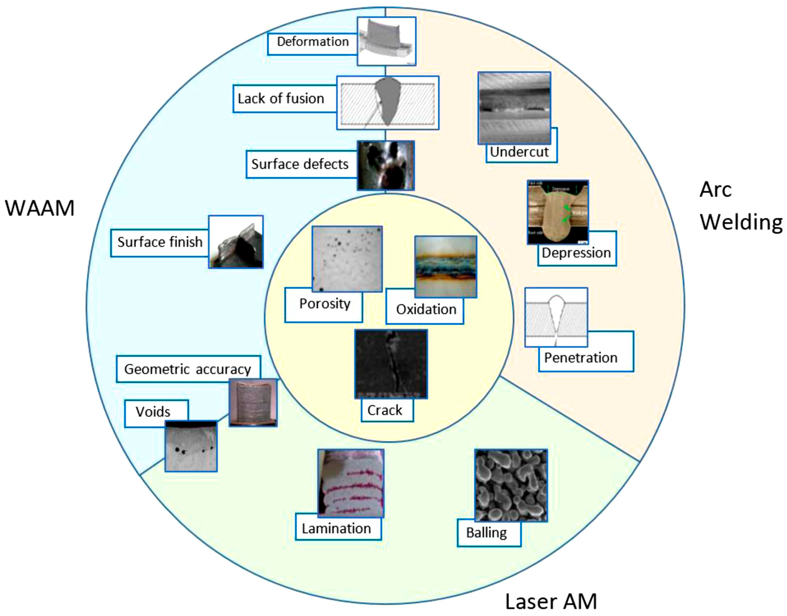
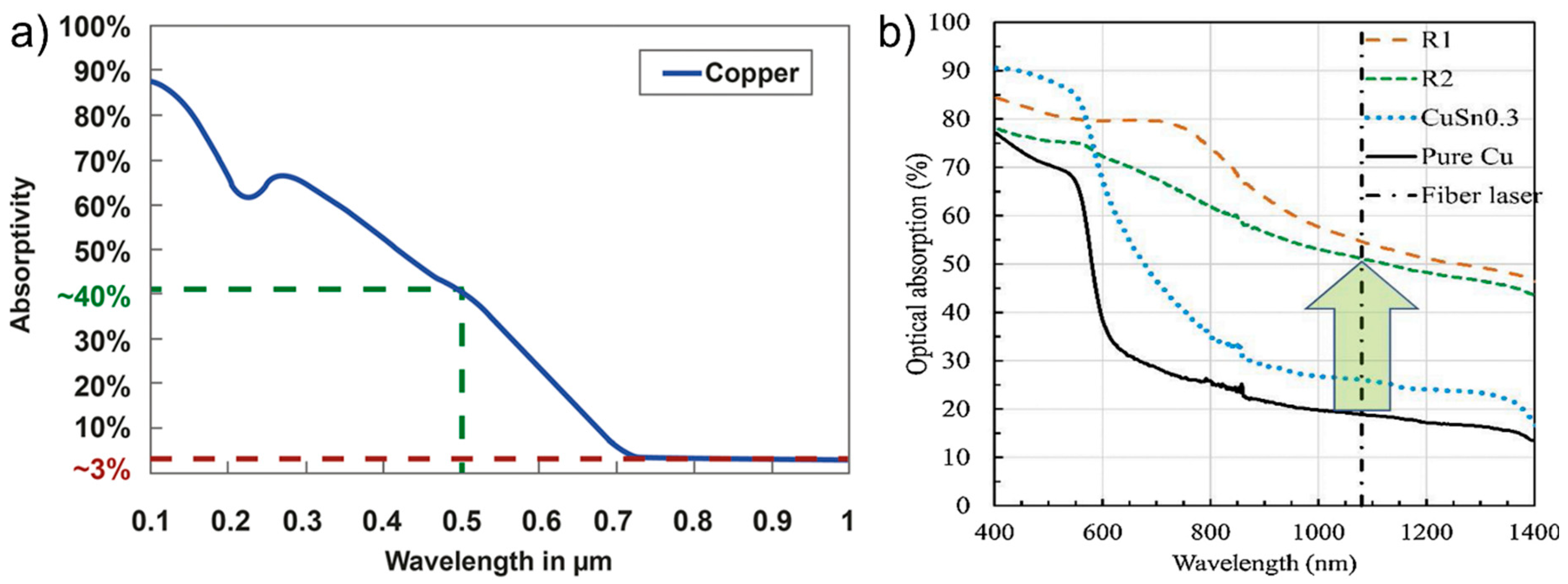
1.3. Challenges Associated with the AM of Copper Alloys
1.4. Solutions to Improve the AM Processability of Copper Alloys
1.4.1. Employing High Power Lasers
1.4.2. Preheating the Powder Bed
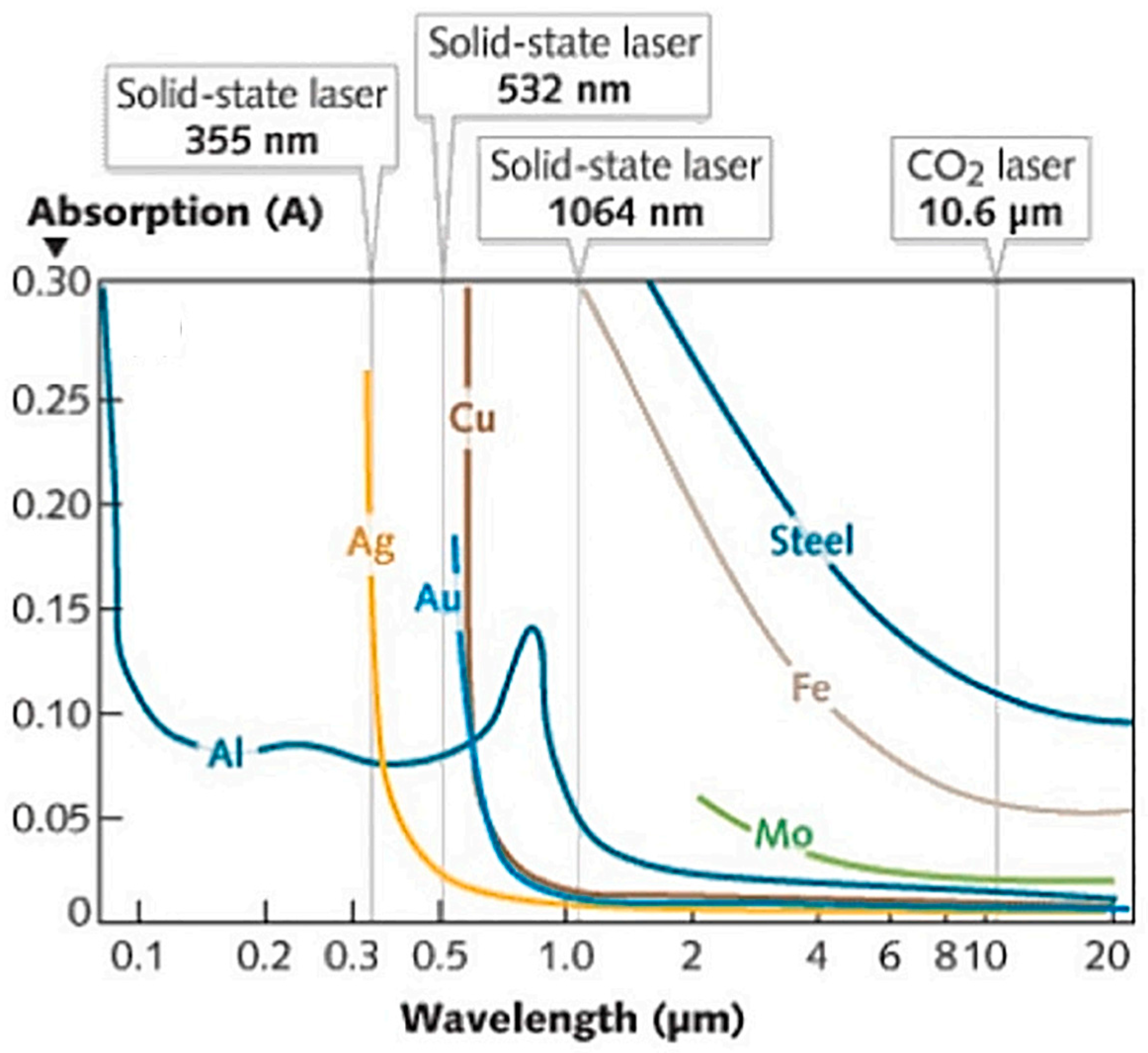
1.4.3. Employing Laser Sources with Lower Wavelengths
1.4.4. Employing a Building Platform with Lower Thermal Conductivity
1.4.5. Addition of Alloying Elements
1.5. Aim and Structure of This Review
2. AM of Cu-Cr Alloys
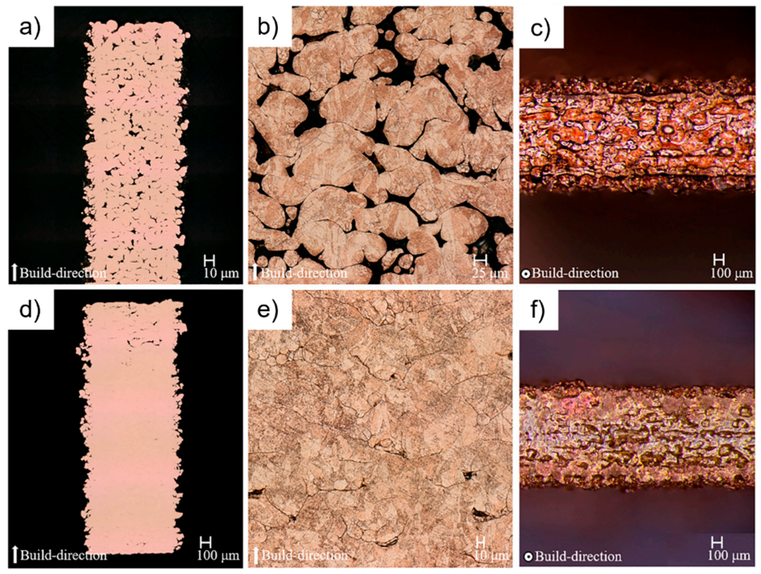
2.1. L-PBF of Cu-Cr Alloys
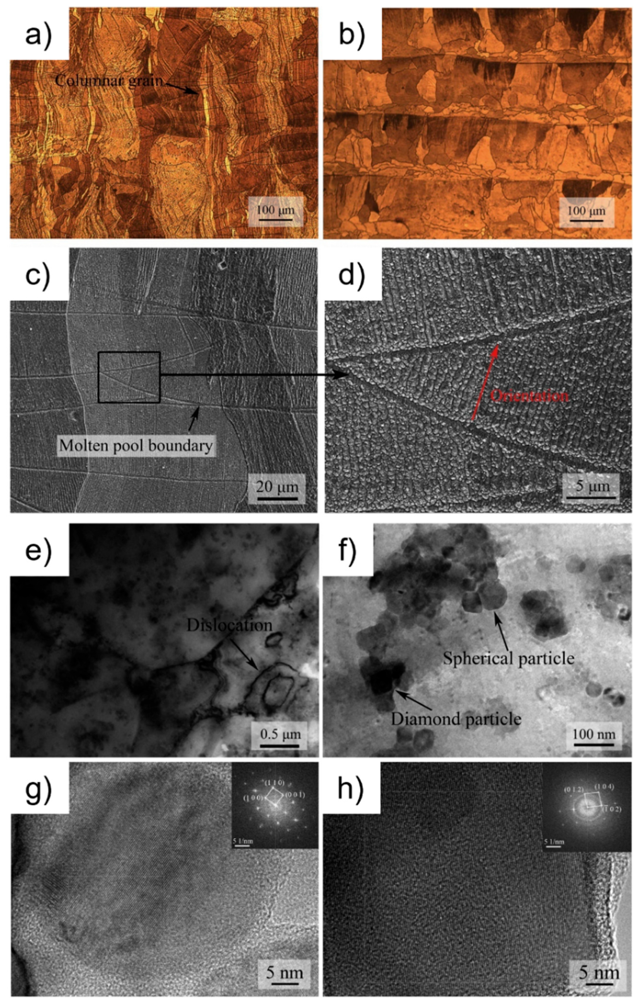
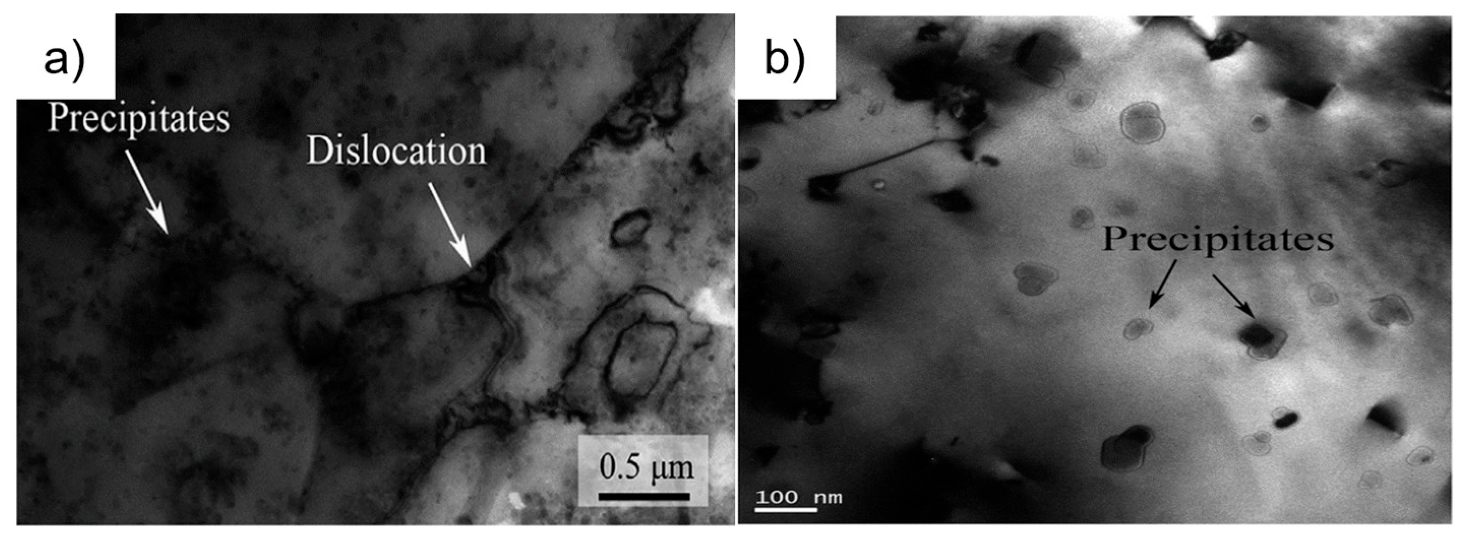
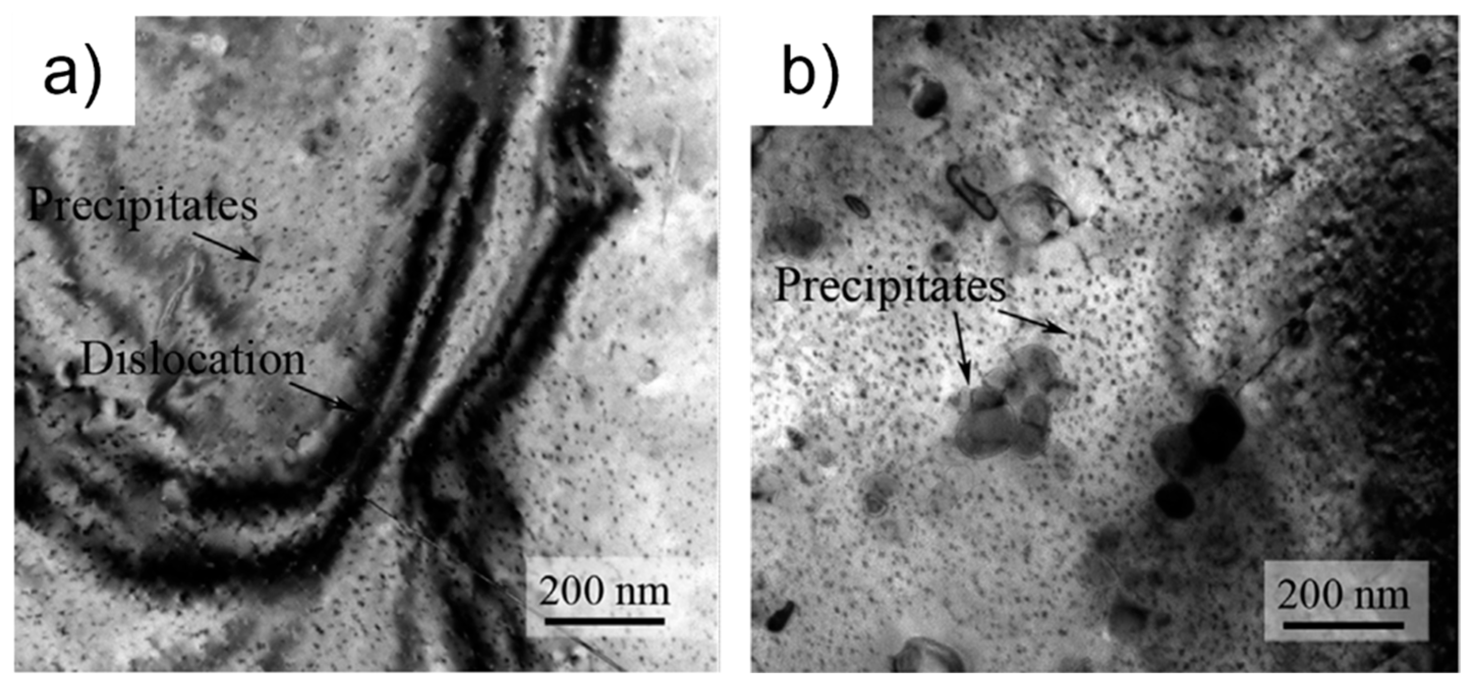
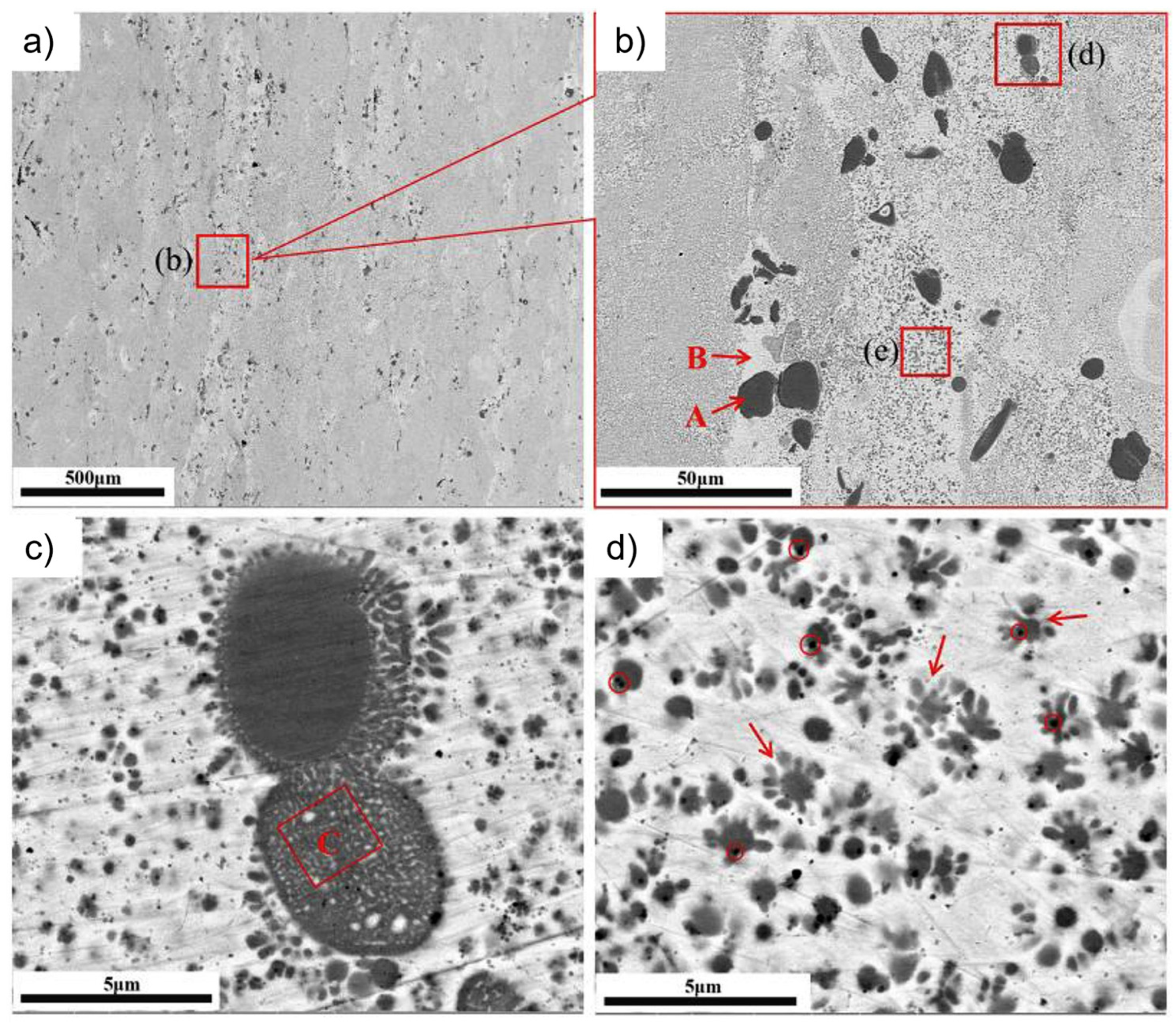
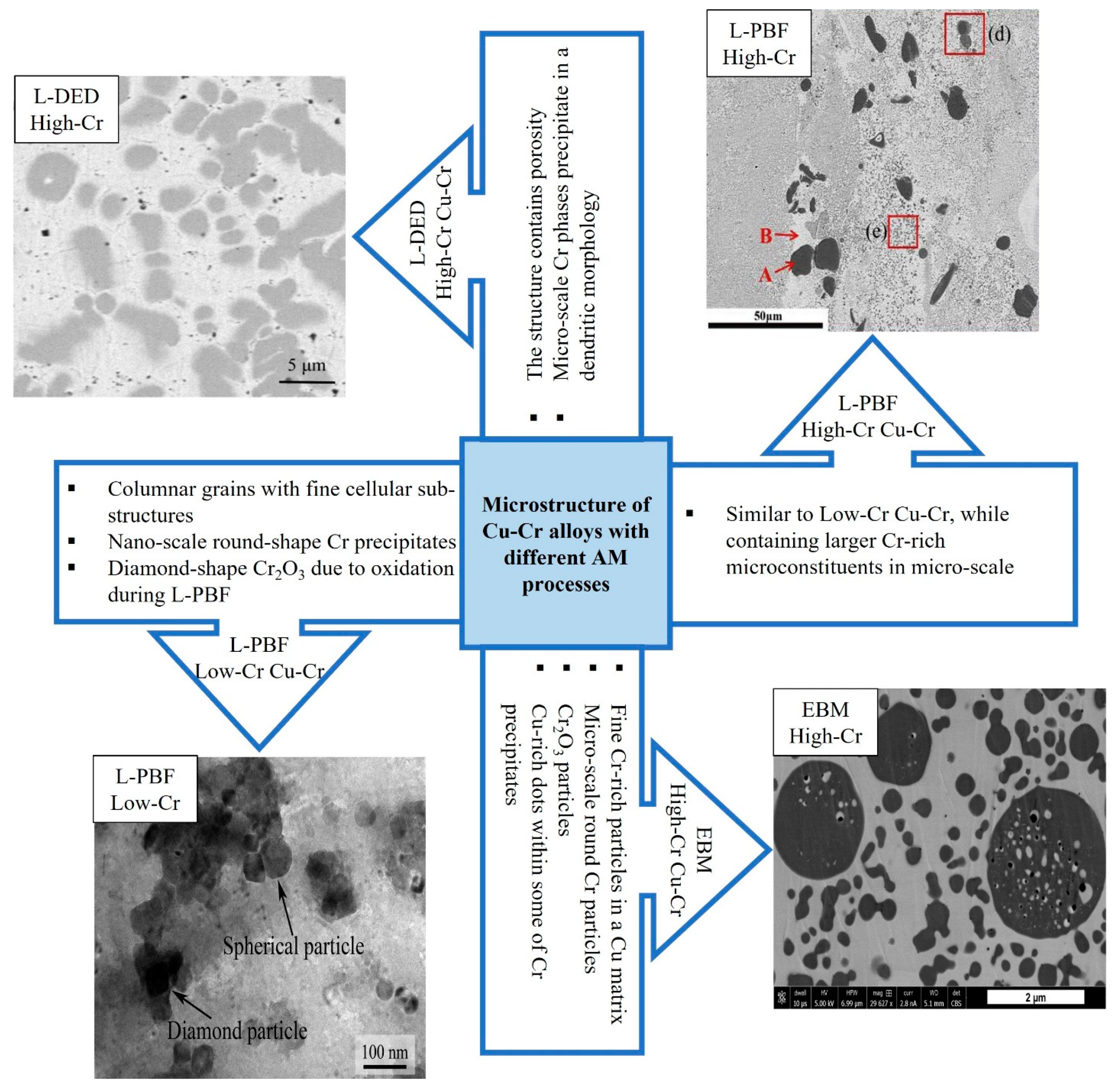
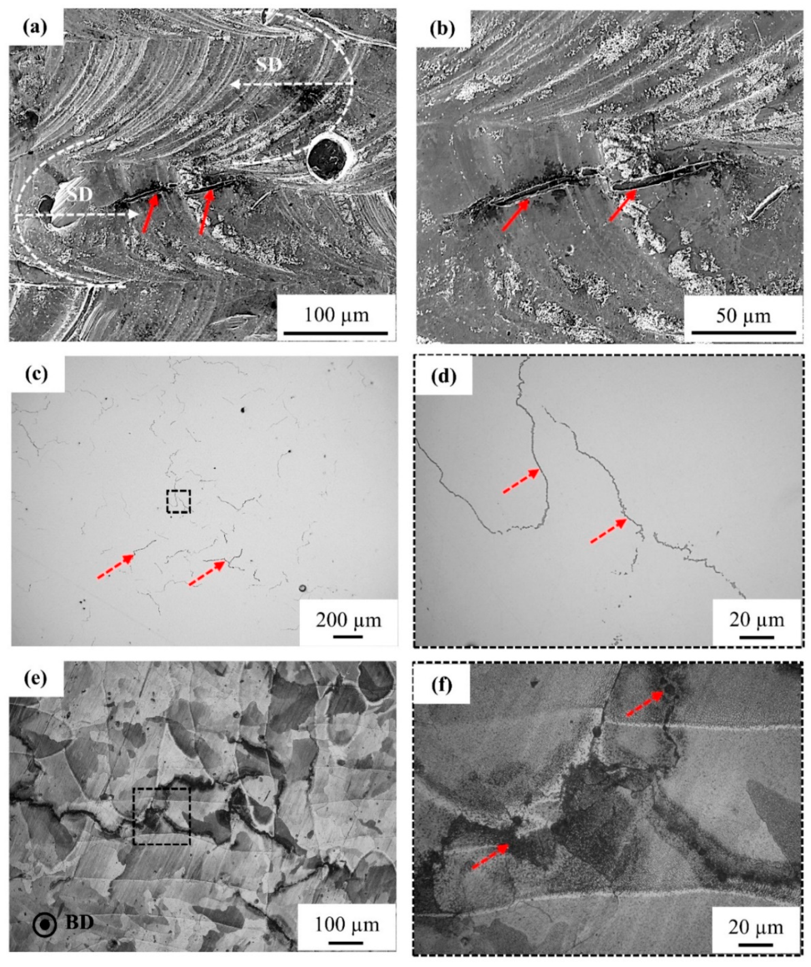
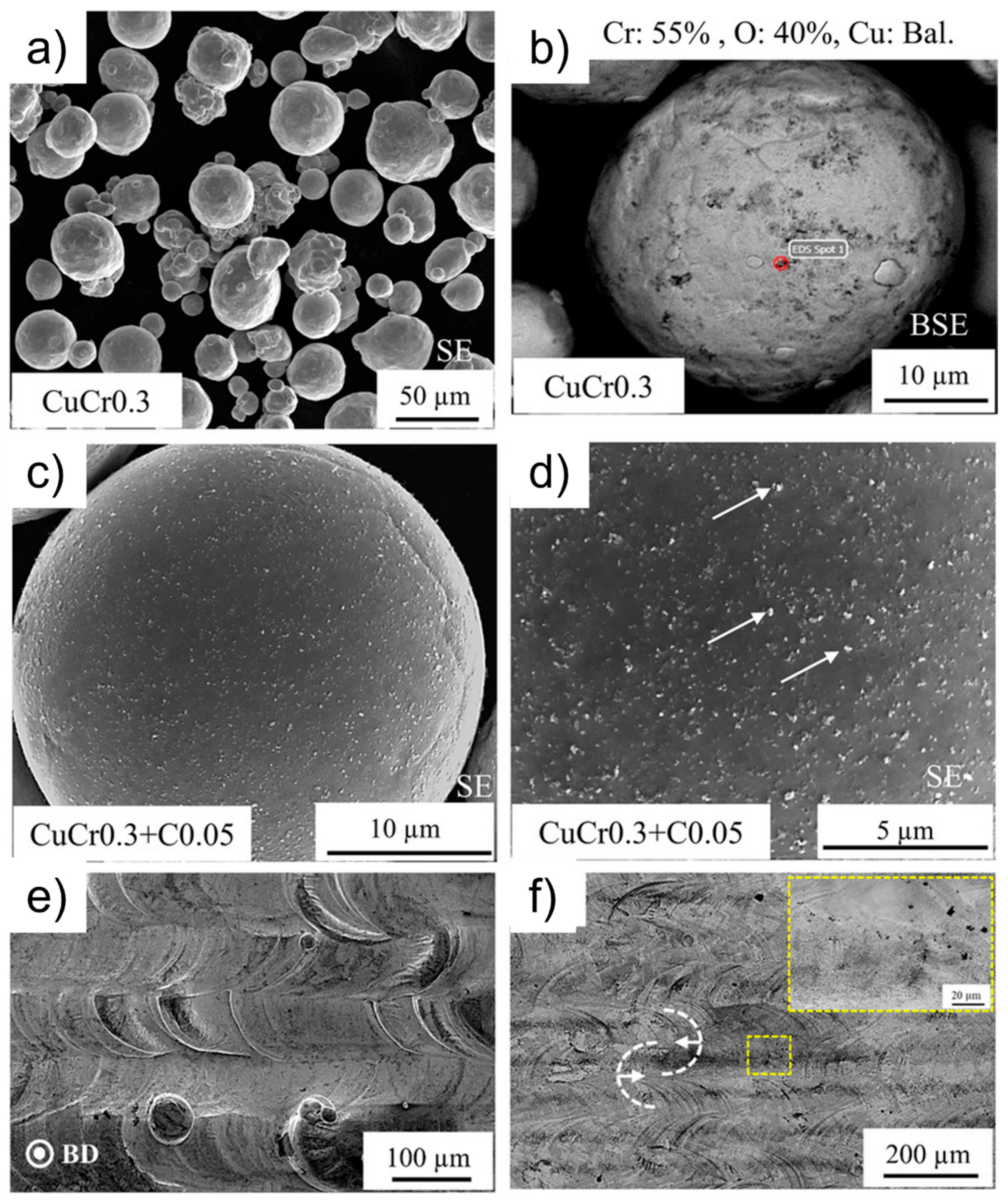
2.1.1. Microstructure of L-PBF-Fabricated Cu-Cr Alloys
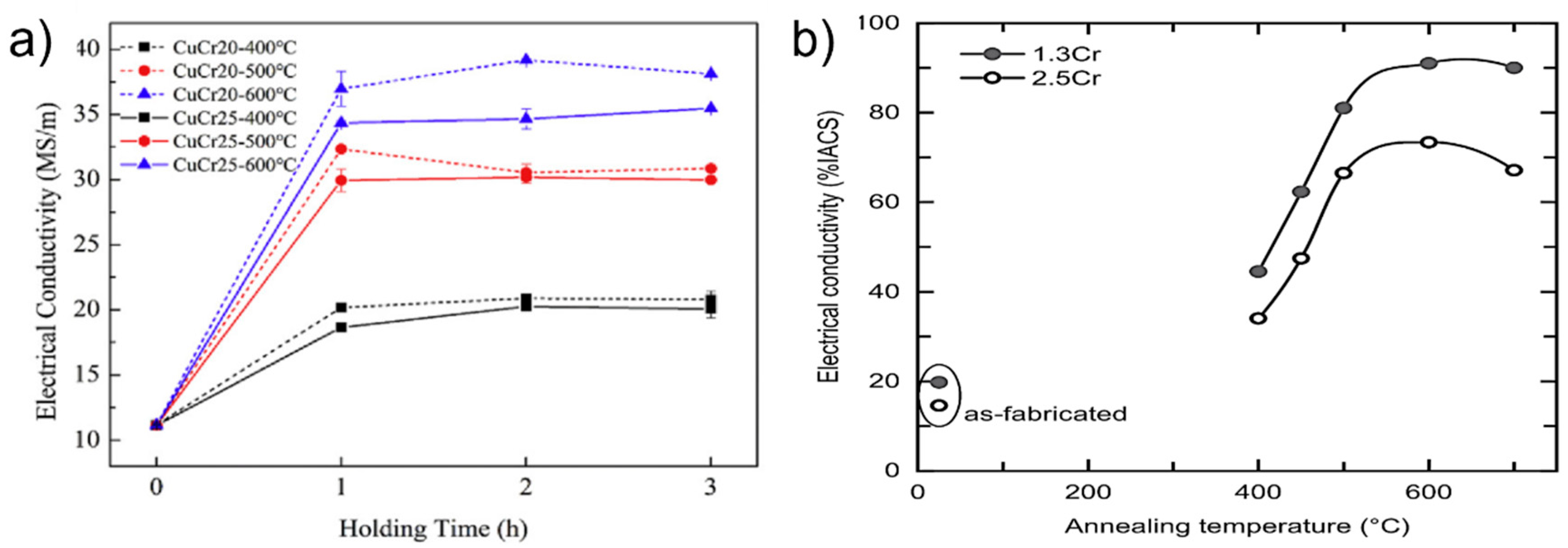
2.1.2. Electrical Conductivity of L-PBF-fabricated Cu-Cr Alloys
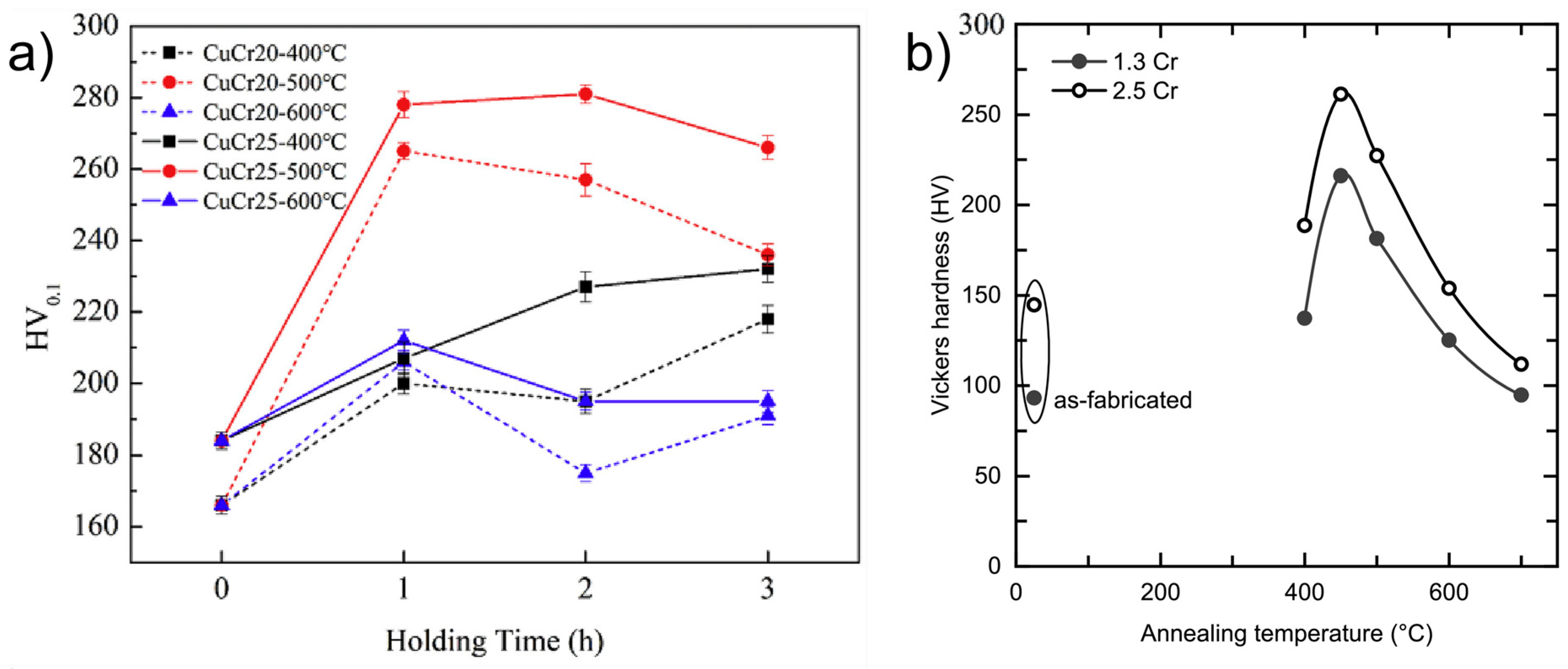
2.1.3. Hardness of L-PBF-Fabricated Cu-Cr Alloys
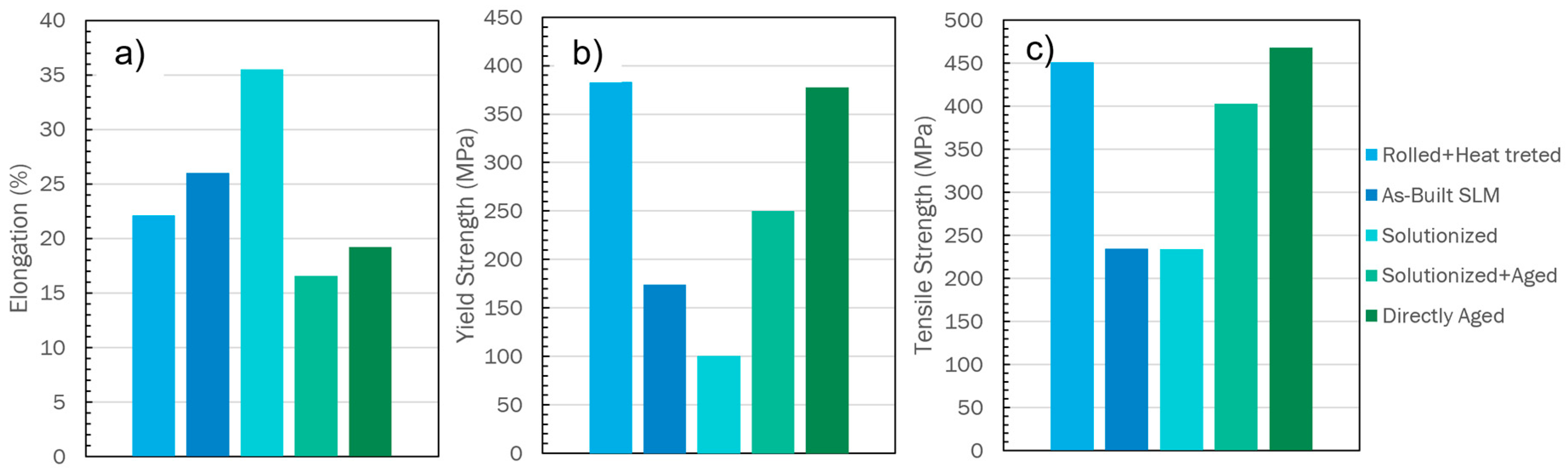
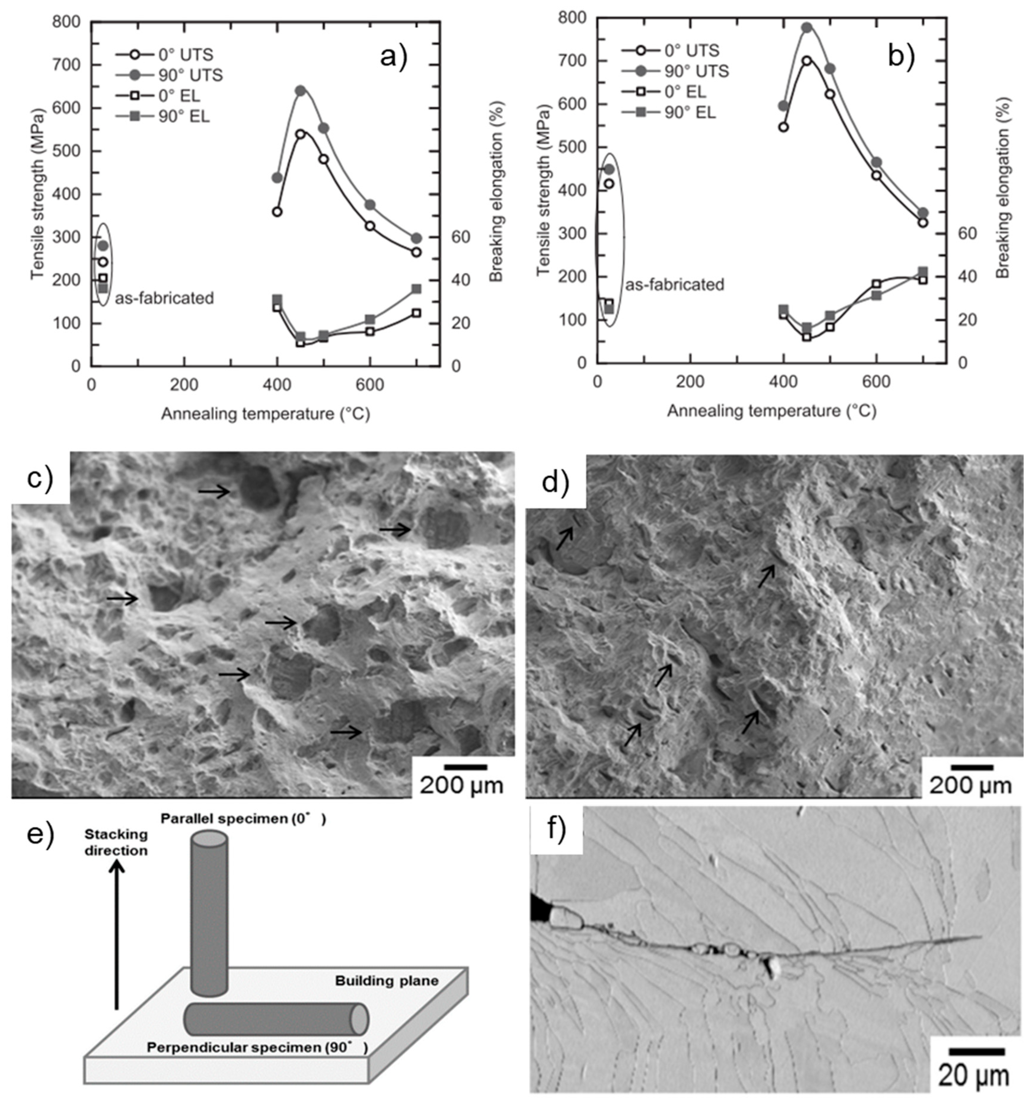
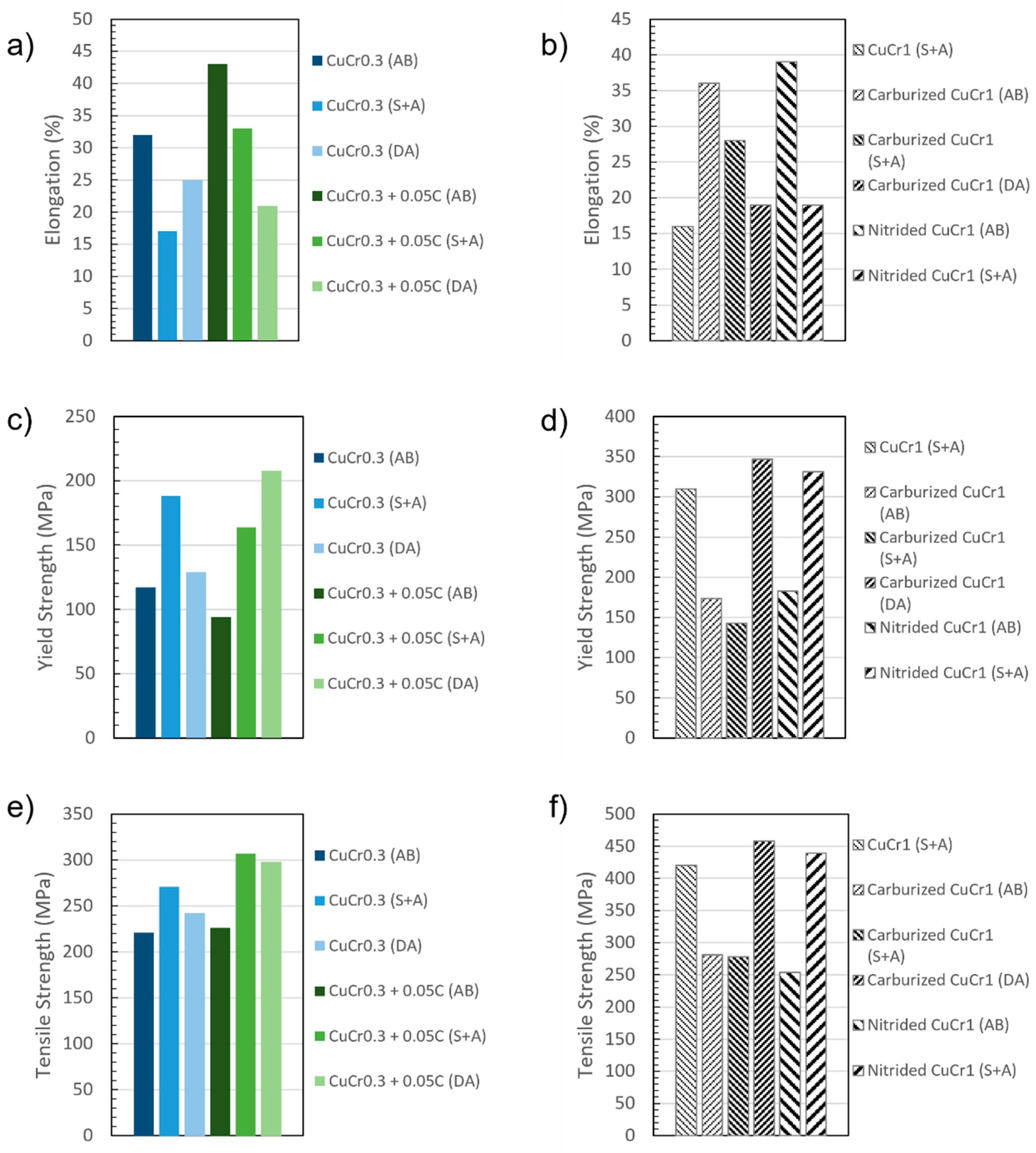
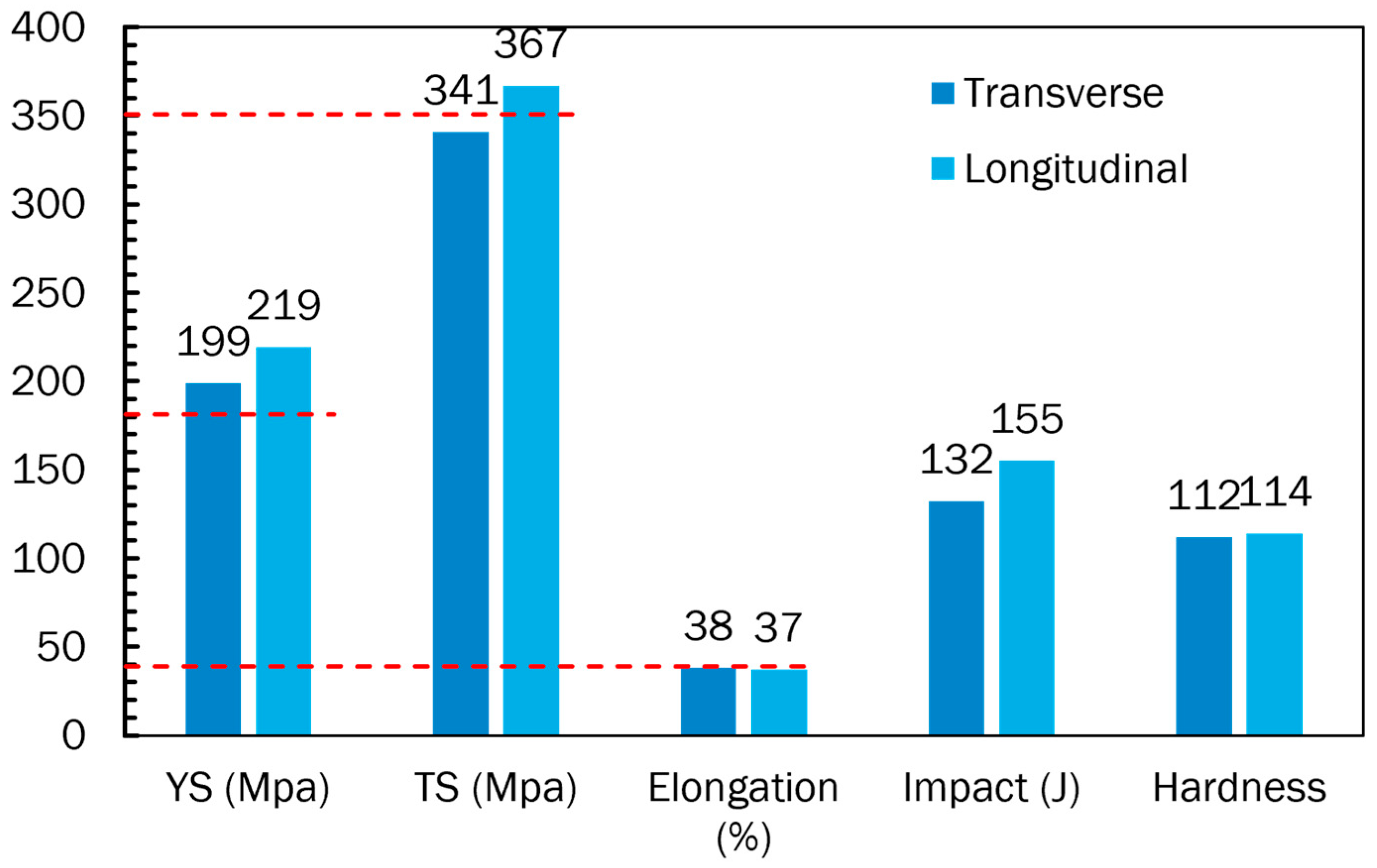
2.1.4. Strength and Ductility of L-PBF-Fabricated Cu-Cr Alloys
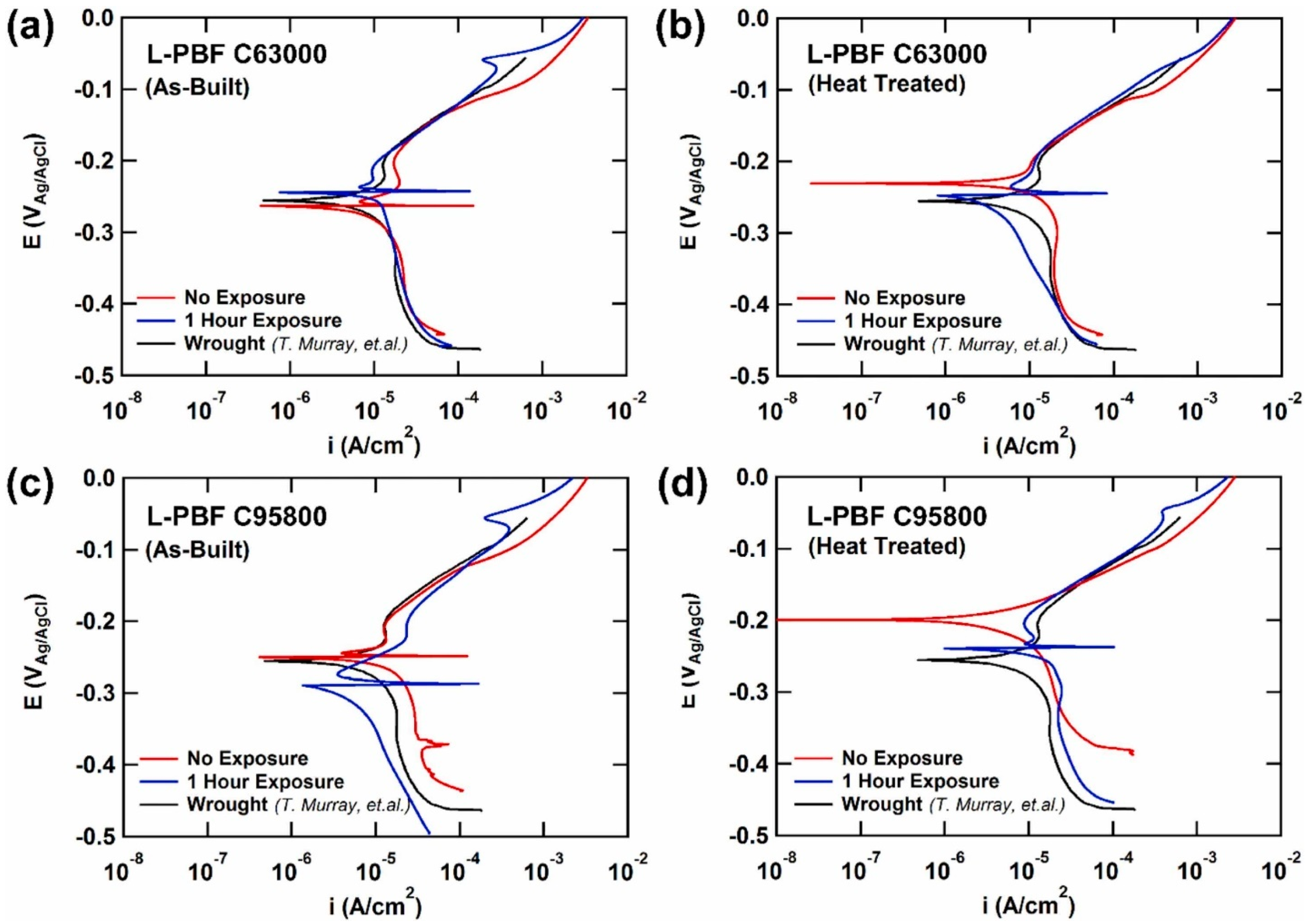
2.1.5. Corrosion Behavior of L-PBF-Fabricated Cu-Cr Alloys
2.2. DED of Cu-Cr Alloys
2.2.1. Microstructure of L-DED-Fabricated Cu-Cr Alloys
2.2.2. Electrical Conductivity of L-DED-Fabricated Cu-Cr Alloys
2.2.3. Hardness, Strength, and Ductility of L-DED-Fabricated Cu-Cr Alloys
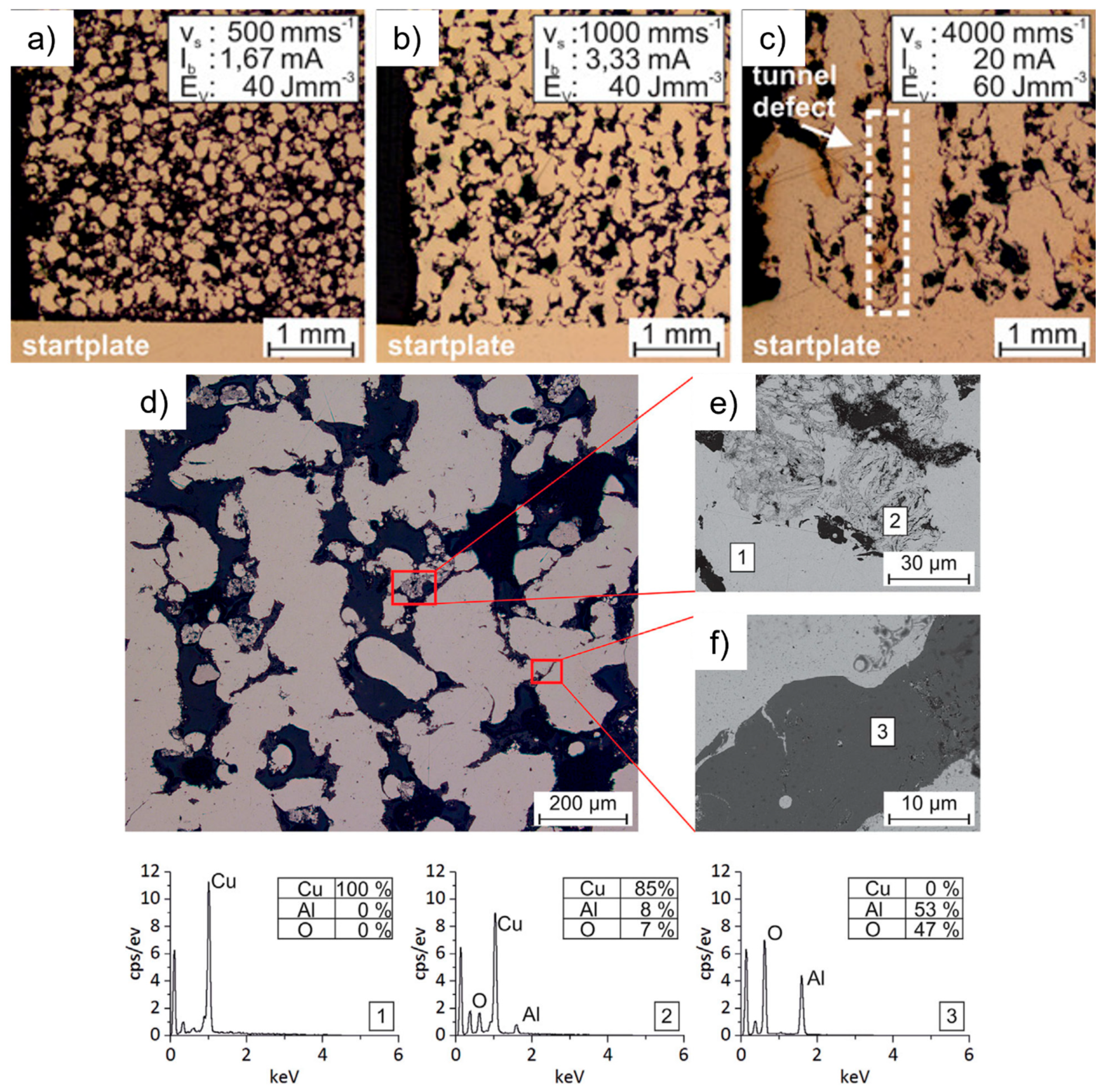
2.3. EBM of Cu-Cr Alloys
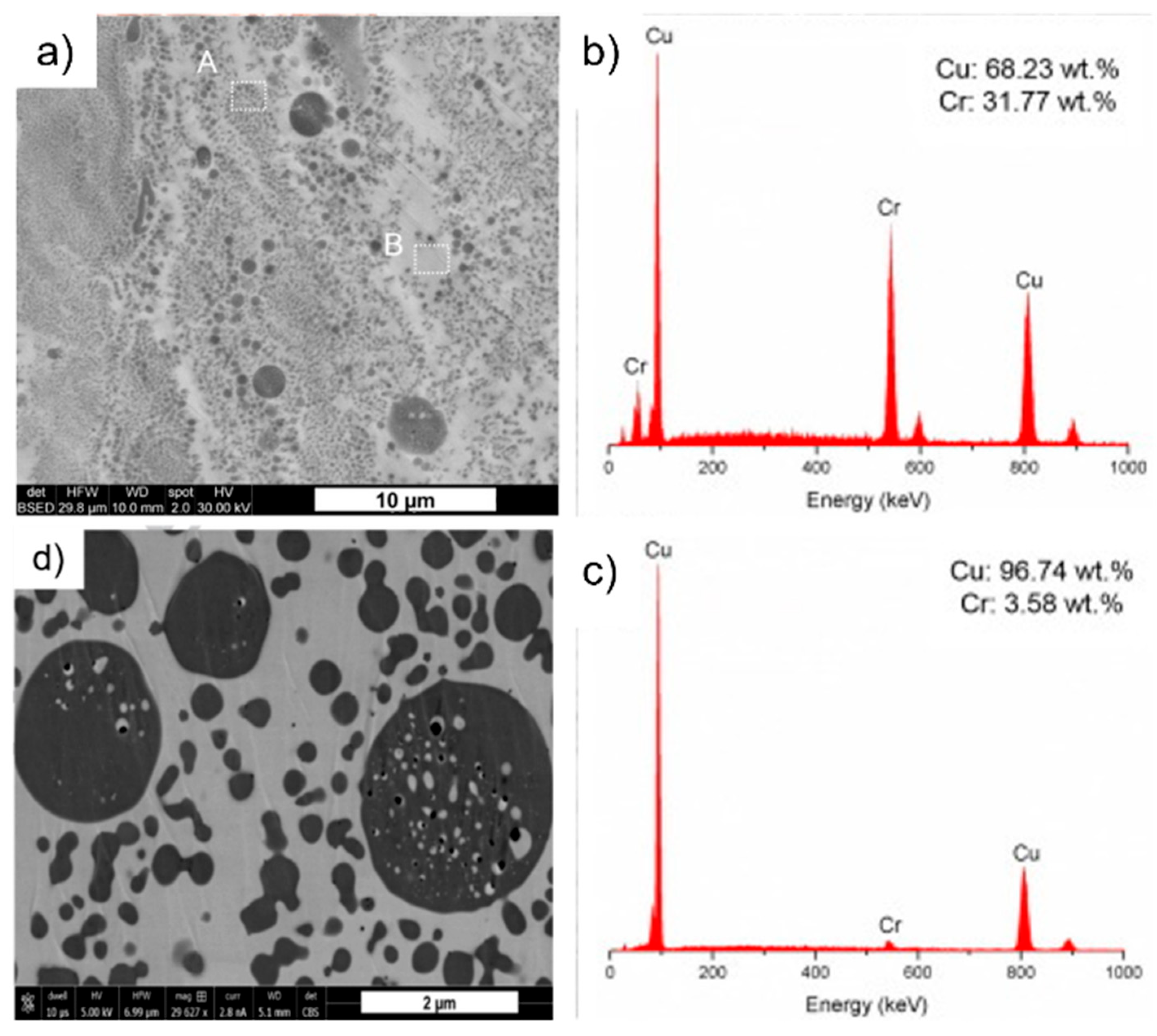
Microstructure of EBM-Fabricated Cu-Cr Alloys
3. AM of Cu-Ni Alloys
3.1. L-PBF of Cu-Ni Alloys
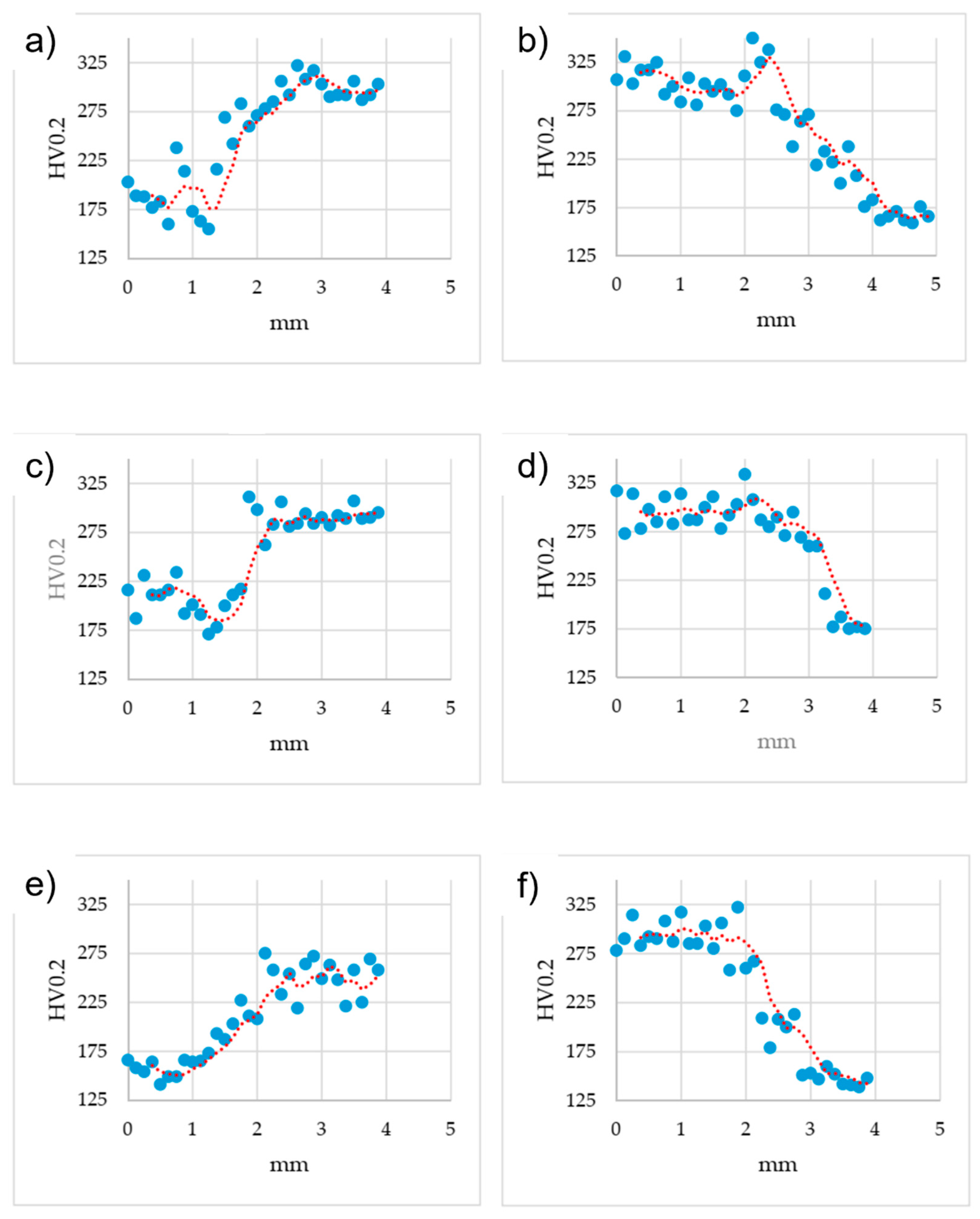
3.1.1. Microstructure of L-PBF-Fabricated Cu-Ni Alloys
3.1.2. Corrosion Behavior of L-PBF-Fabricated Cu-Ni Alloys
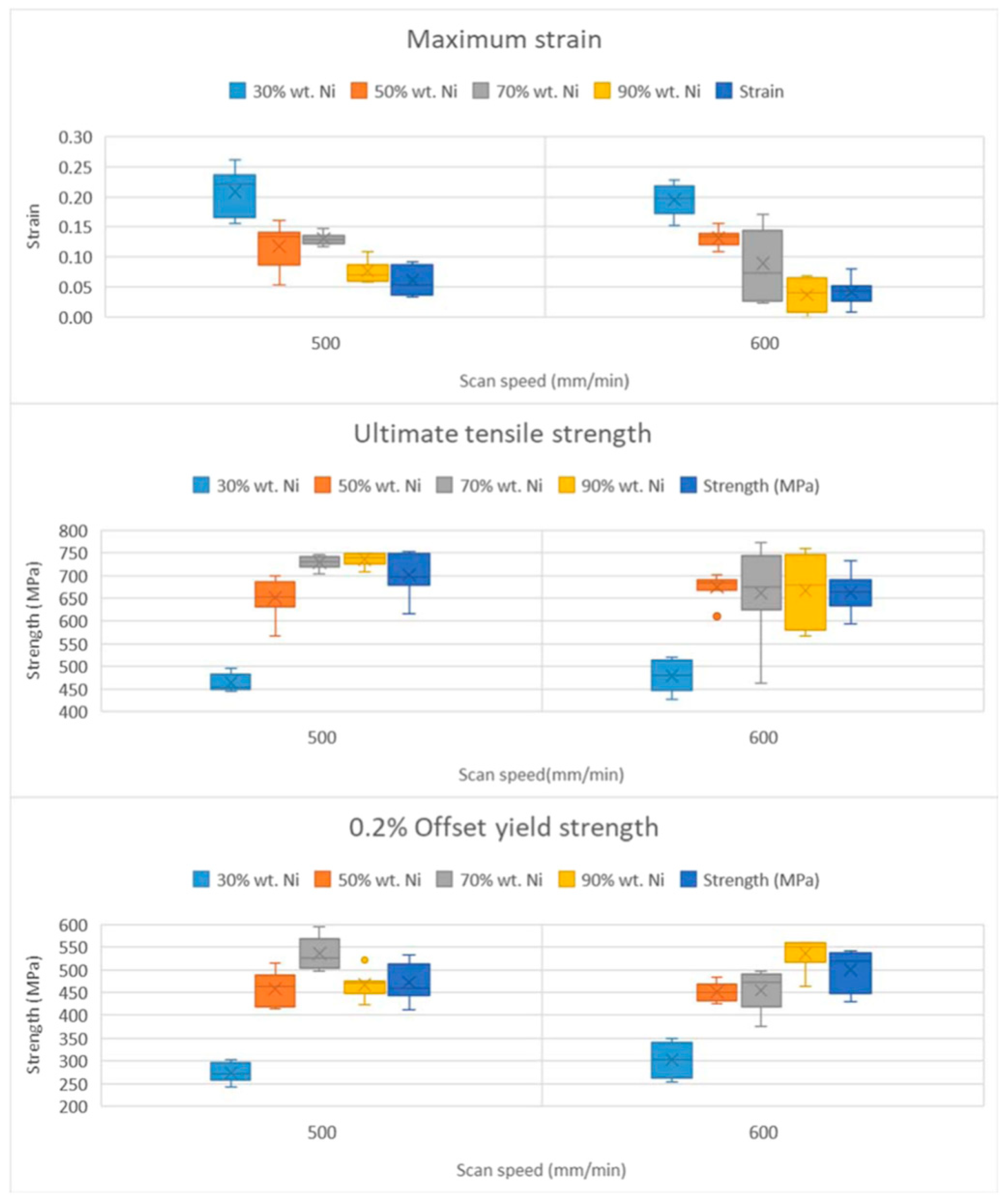
3.1.3. Hardness and Strength of L-PBF-Fabricated Cu-Ni Alloys
3.2. DED of Cu-Ni Alloys
3.2.1. Microstructure of DED-Fabricated Cu-Ni Alloys
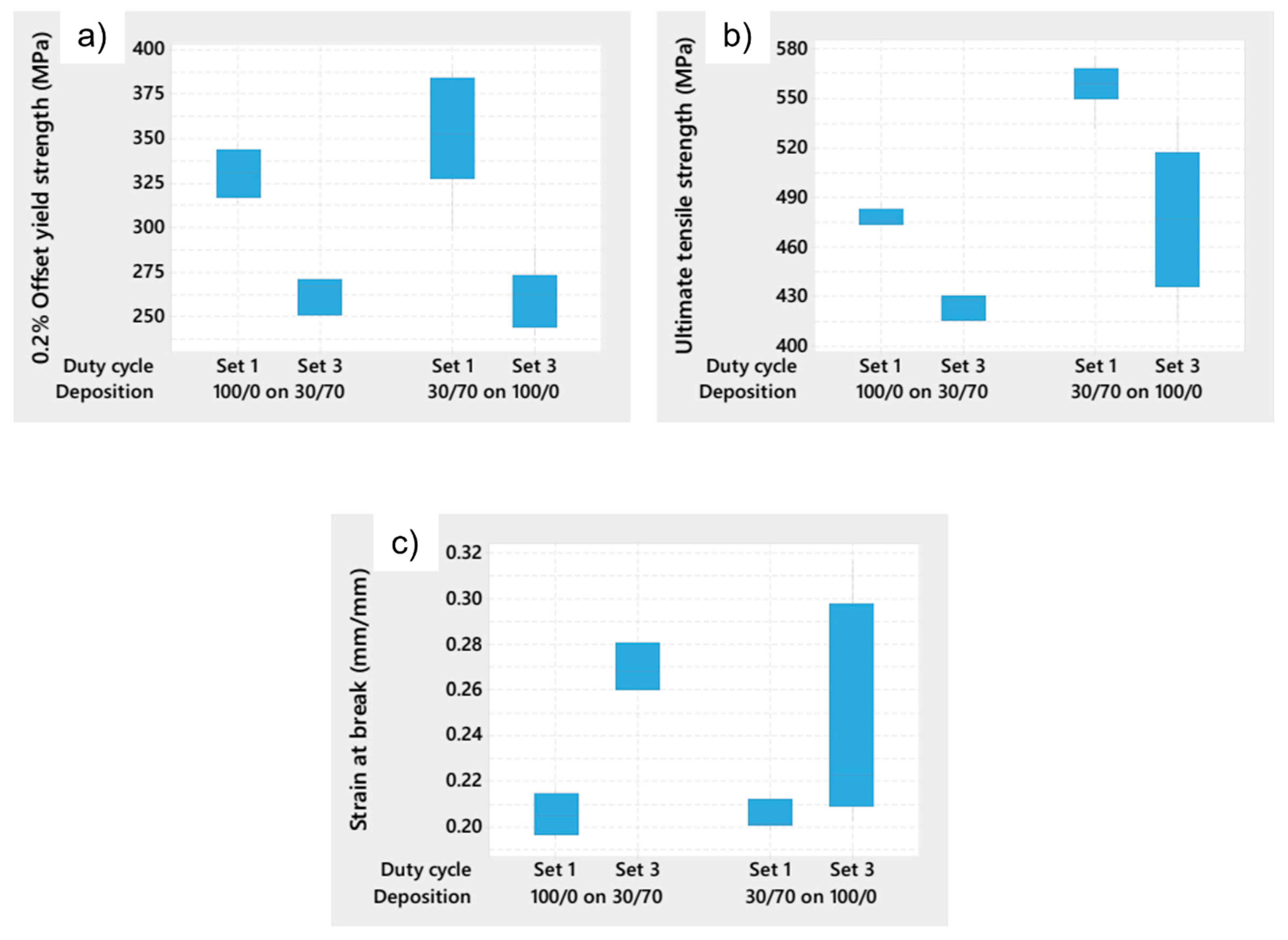
3.2.2. Hardness, Strength, and Ductility of DED-Fabricated Cu-Ni Alloys
3.2.3. Thermal/Electrical Conductivity of DED-Fabricated Cu-Ni Alloys
3.2.4. Corrosion Behavior of DED-Fabricated Cu-Ni Alloys
4. AM of Tin-Bronzes
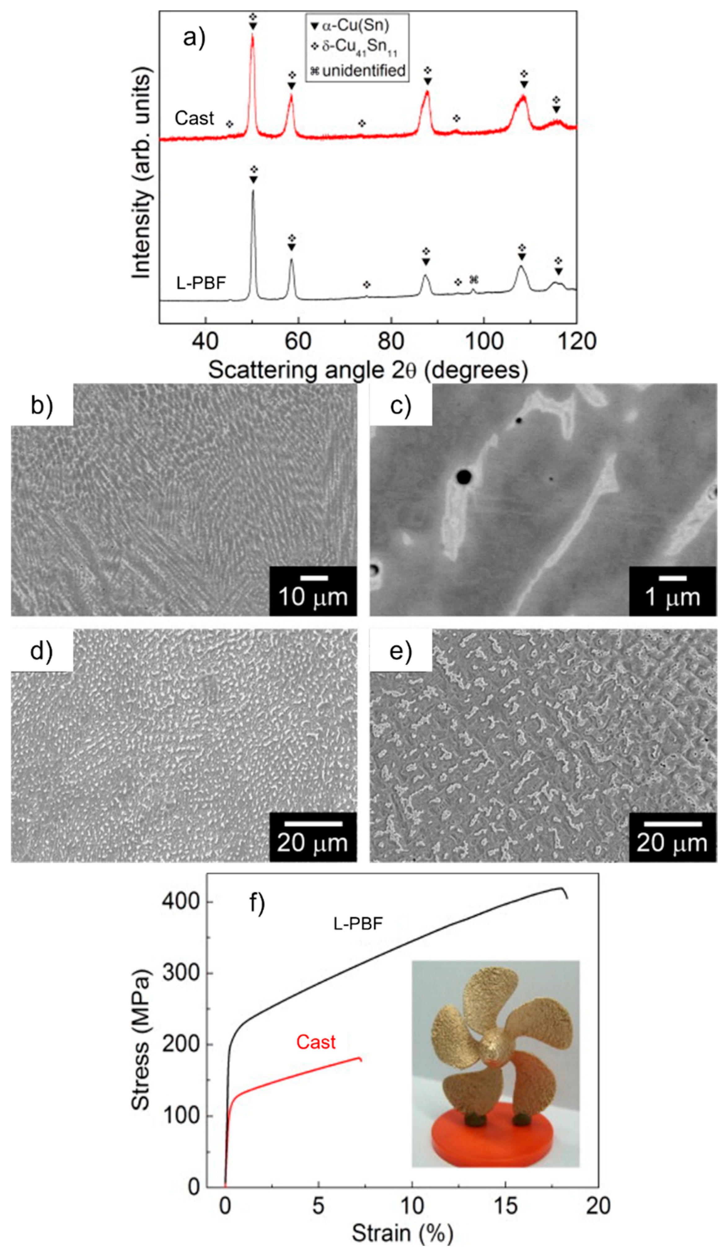
4.1. Microstructure and Mechanical Properties of L-PBF-Fabricated Tin-Bronzes versus the Cast Counterparts
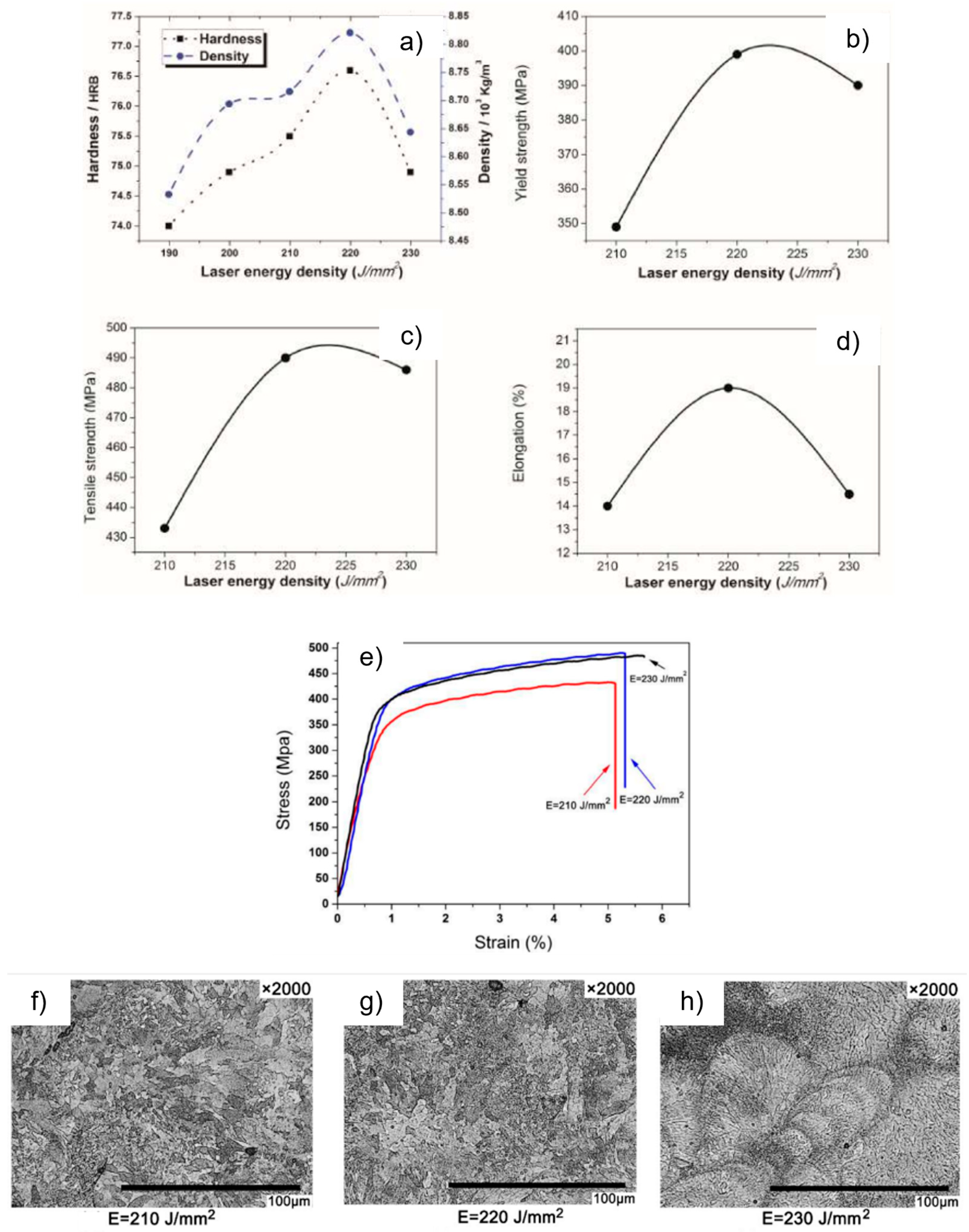
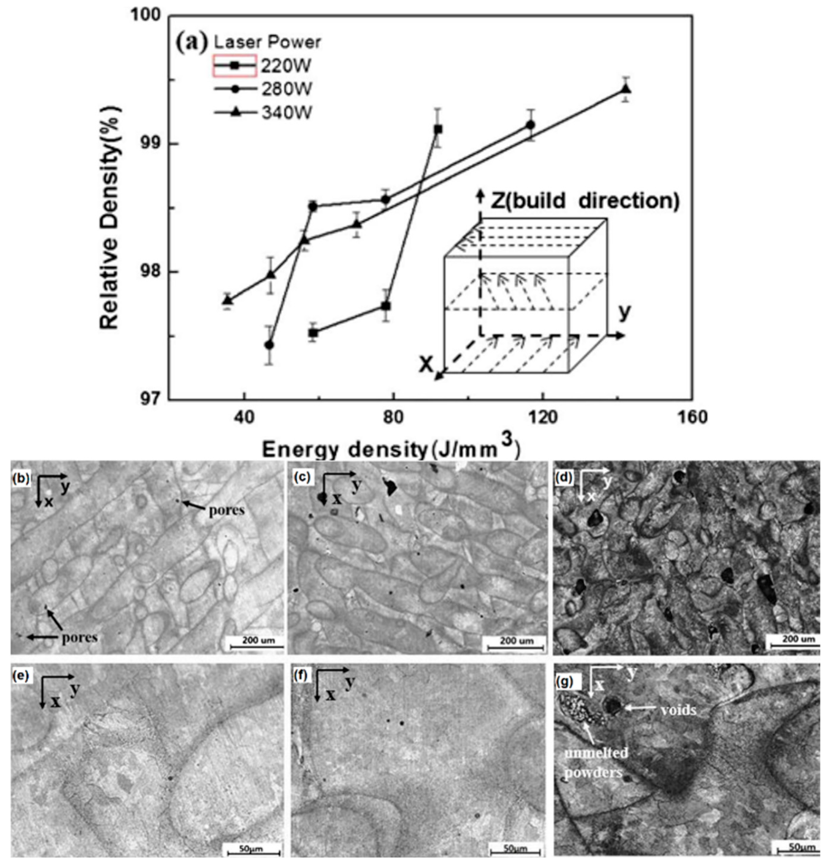
4.2. Effect of Laser Energy Density on the Microstructure, Relative Density, and Mechanical Properties of L-PBF-Produced Tin-Bronzes
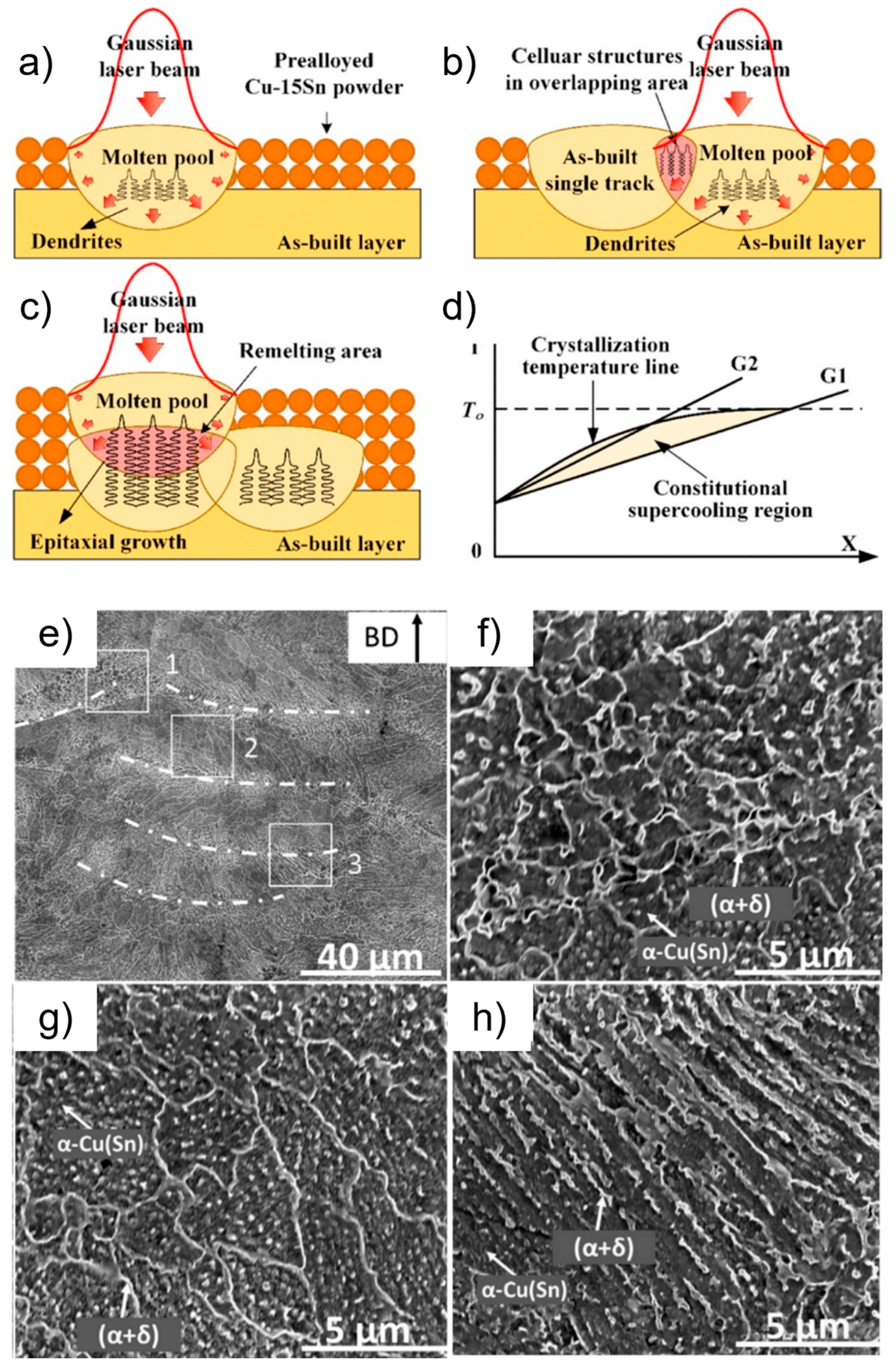
4.3. Solidification Behavior at Different Regions of L-PBF Tin-Bronzes
4.4. Post-Printing Annealing of L-PBF Tin-Bronzes
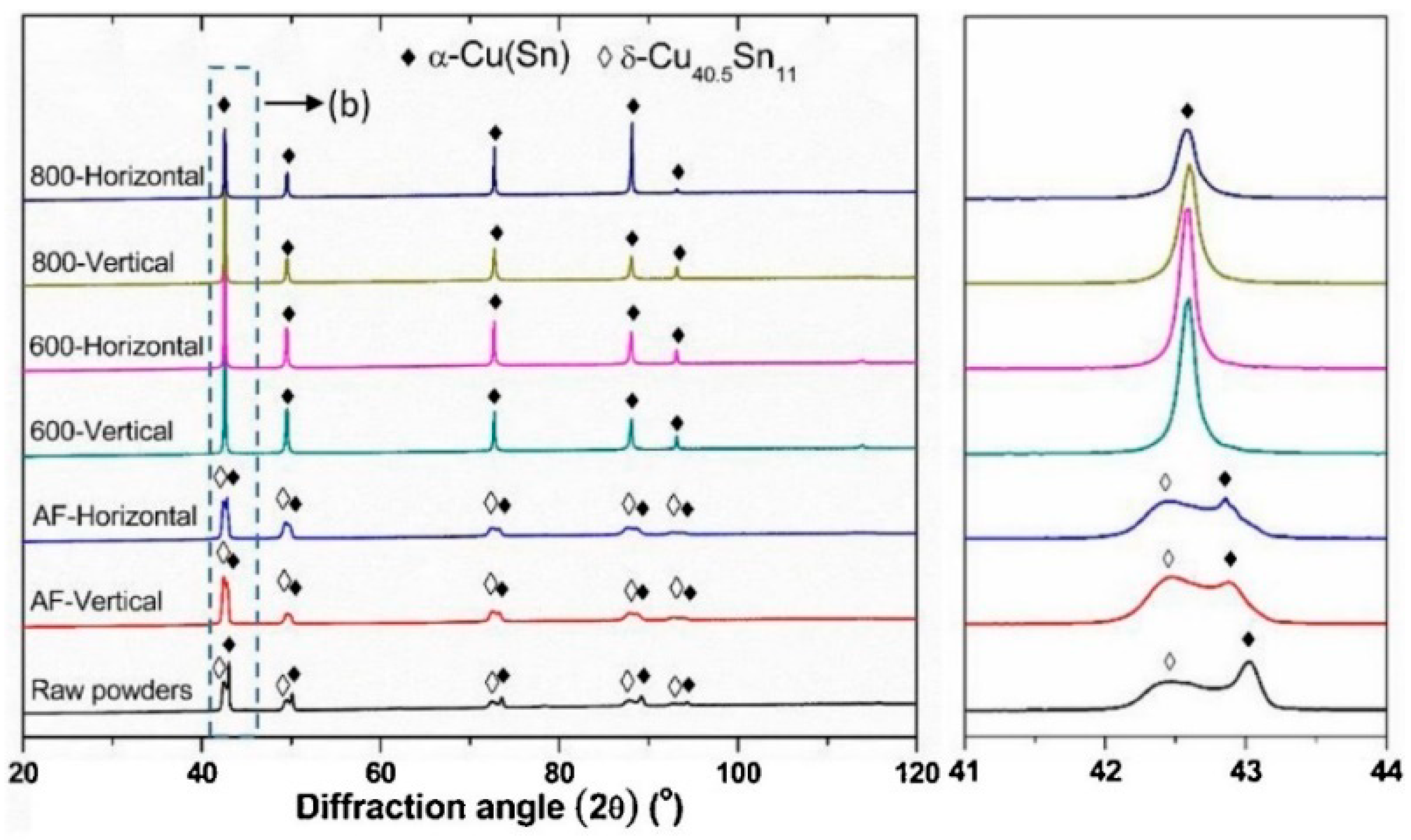
4.4.1. Effect of Post-Printing Annealing on the Microstructure of L-PBF Tin-Bronzes
4.4.2. Effect of Post-Printing Annealing on the Mechanical Properties of L-PBF Tin-Bronzes
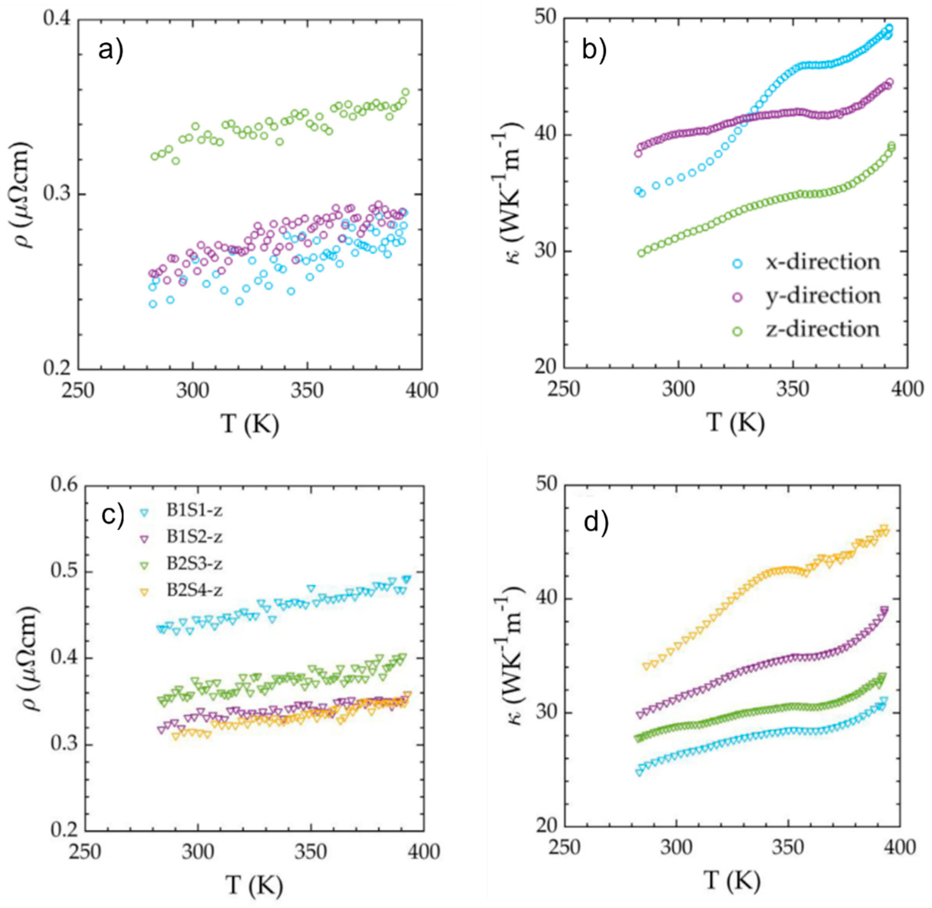
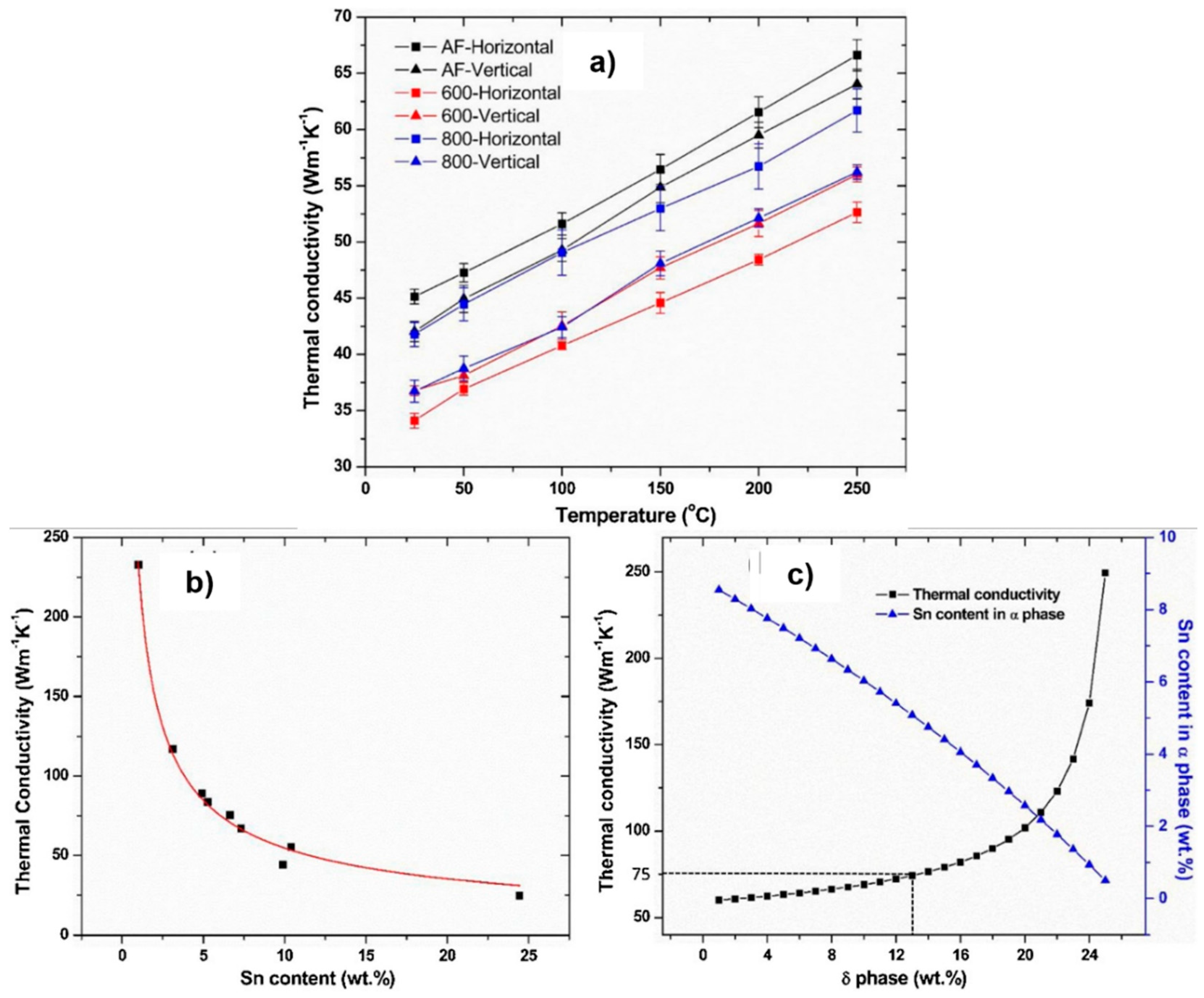
4.4.3. Effect of Post-Printing Annealing on the Thermal Properties of L-PBF Tin-Bronzes
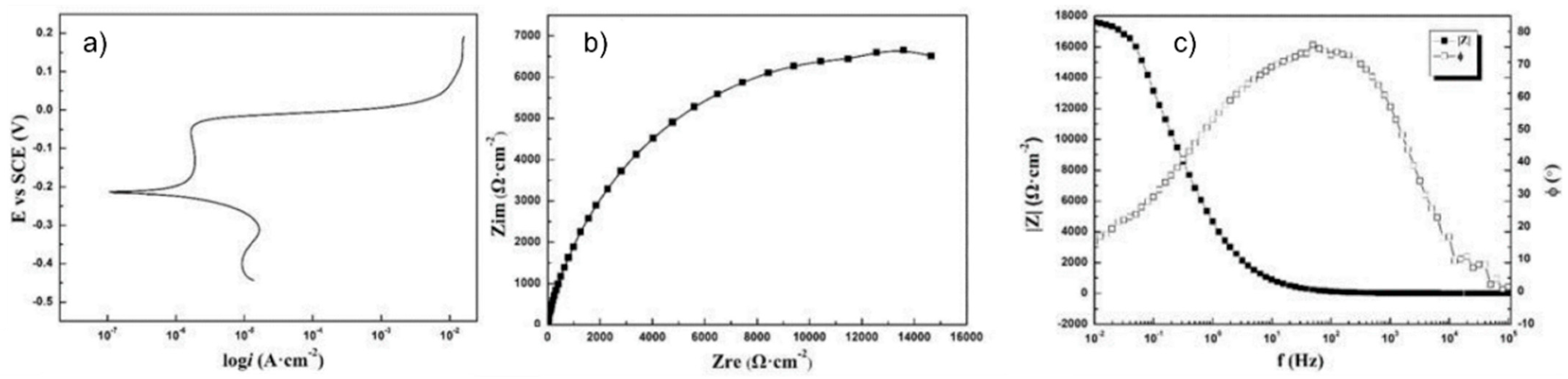
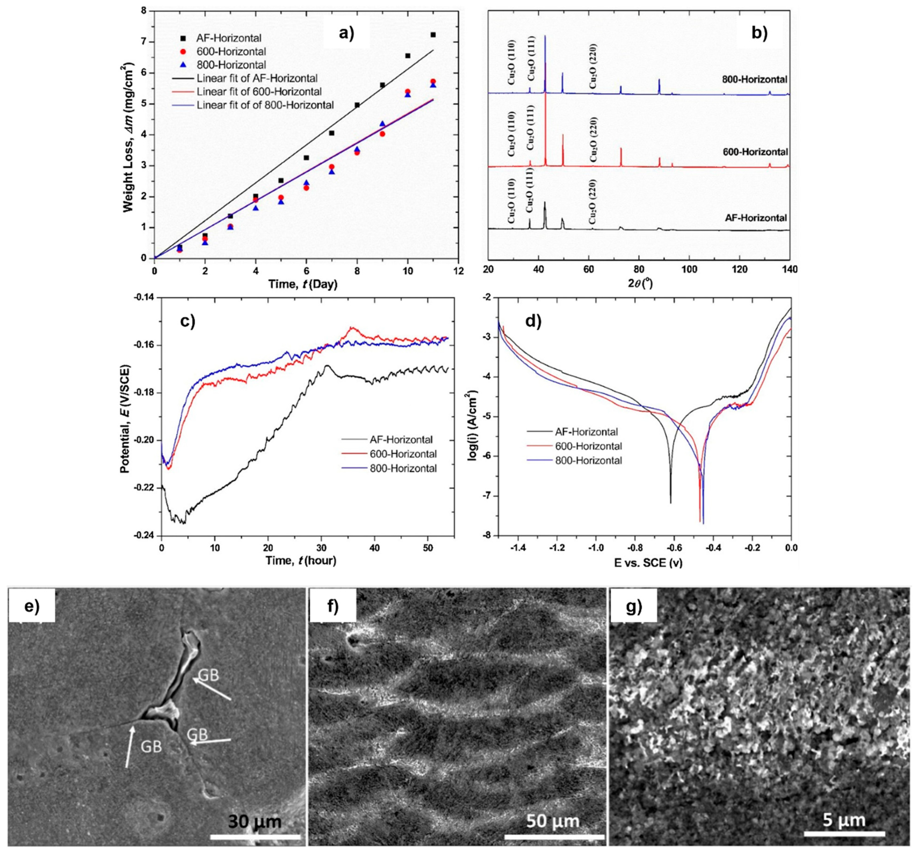
4.4.4. Effect of Post-Printing Annealing on the Corrosion Properties of L-PBF Tin-Bronzes
4.5. AM-Fabricated Bimetal Tin-Bronzes and Dissimilar Metallic Materials
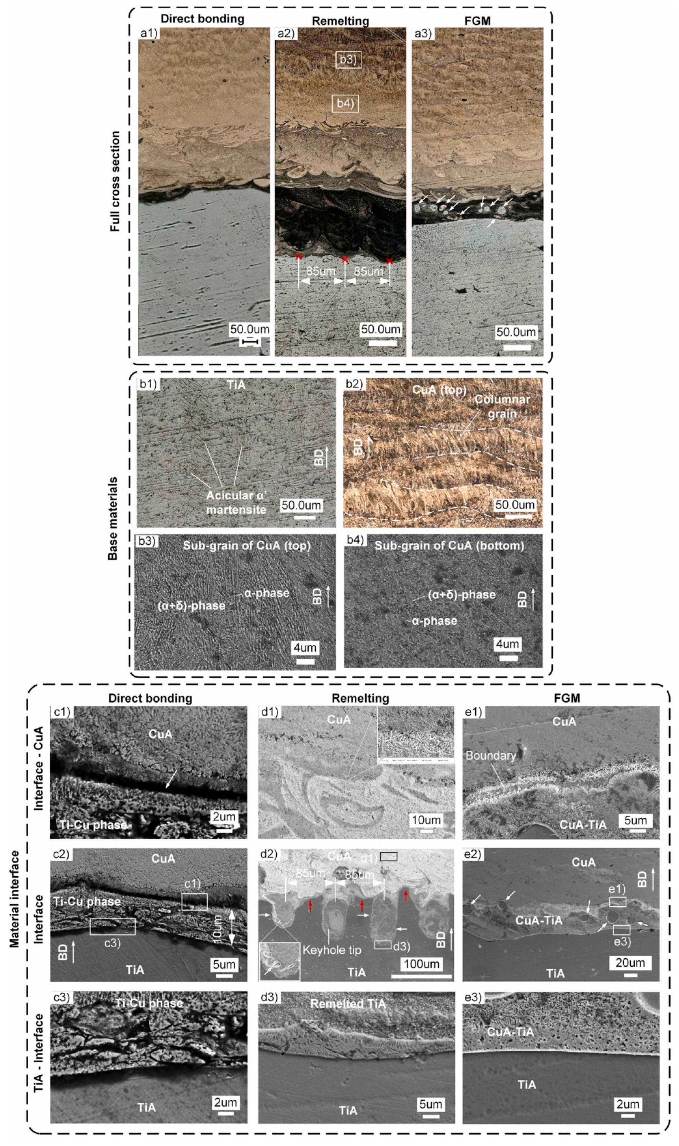
4.5.1. AM of Bimetallic Cu10Sn-Ti6Al4V Structure Using the L-PBF Technique
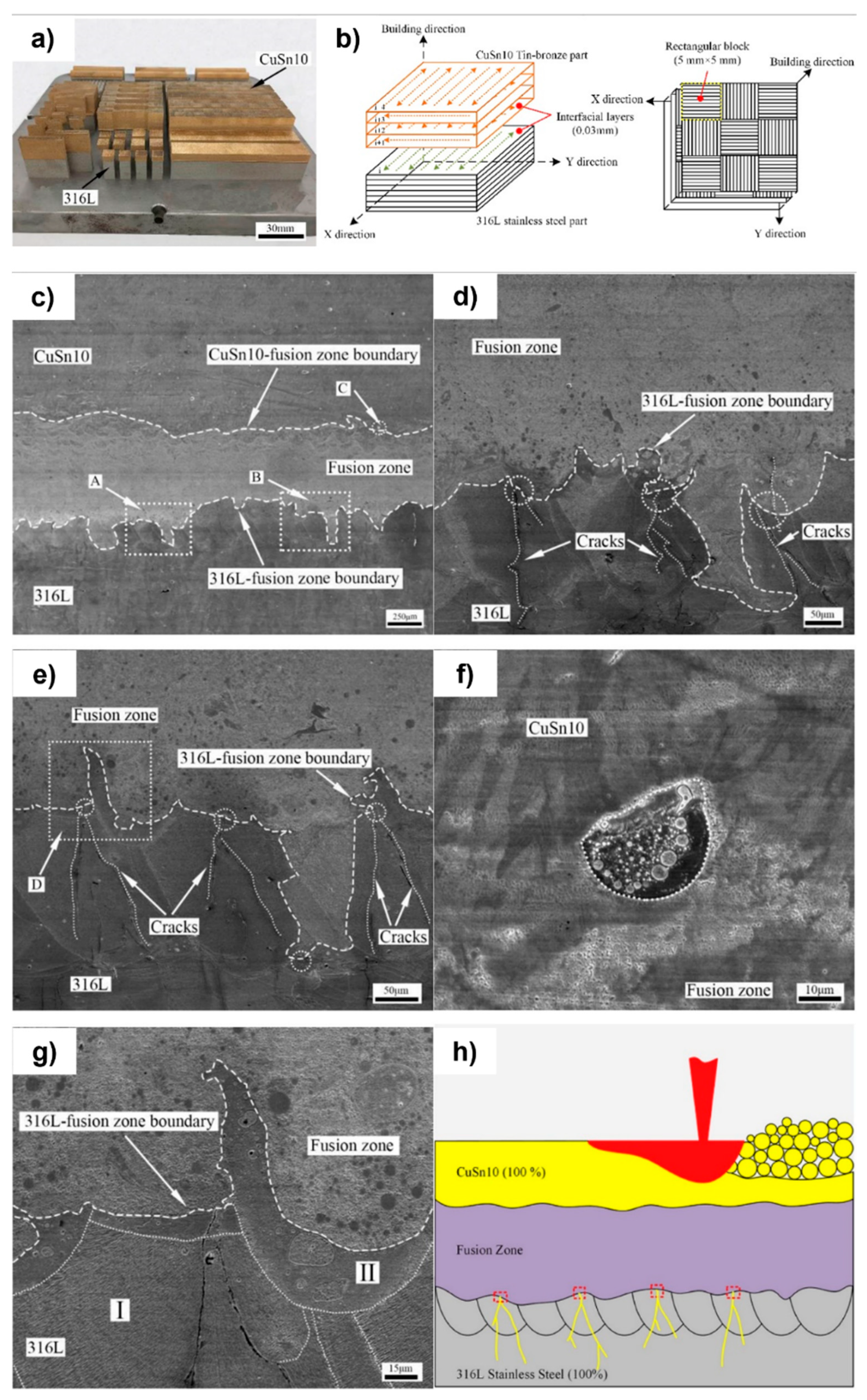
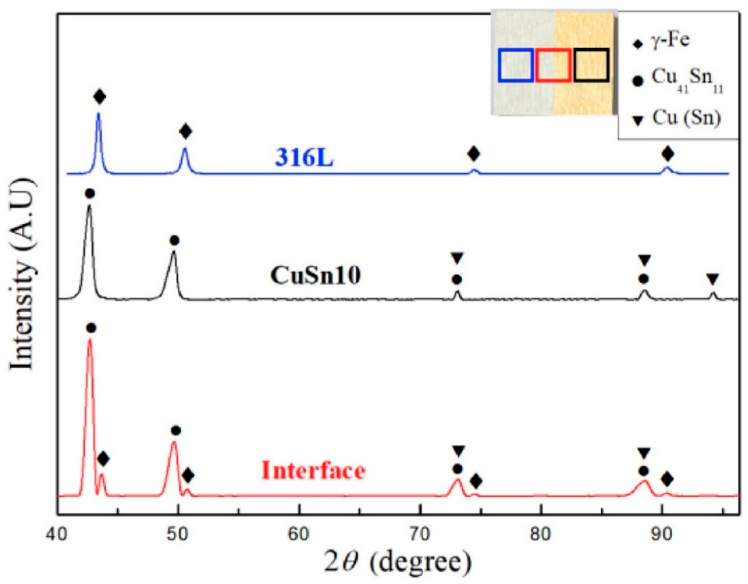
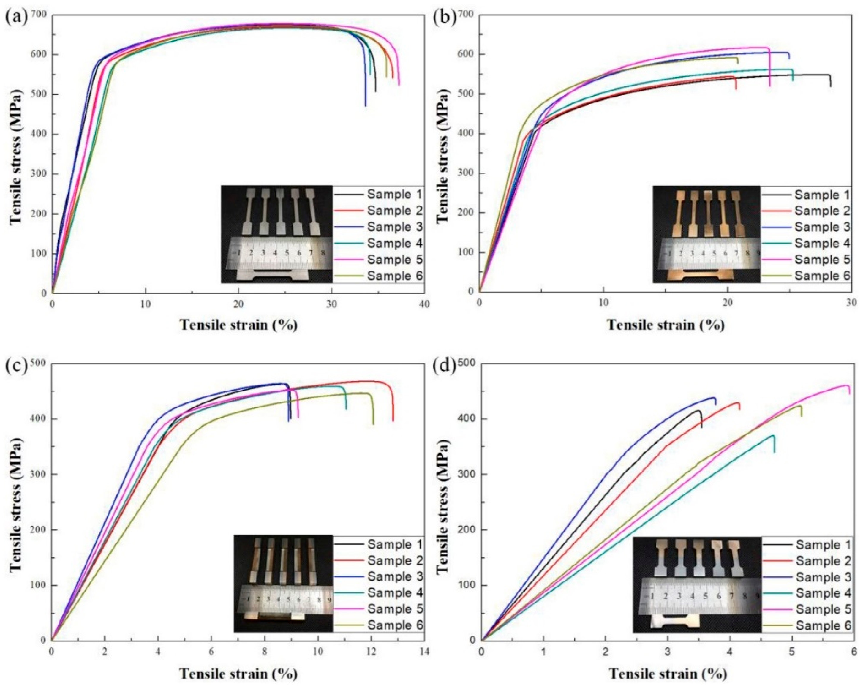
4.5.2. AM of Bimetallic Cu10Sn- 316L Structure Using the L-PBF Technique
4.6. AM of Tin-Bronze Using Alternative Processes
5. AM of NAB Alloys

| AM Process | Alloy | Pre/Post/In-Situ Treatments | Ref. |
|---|---|---|---|
| WAAM (CMT) | AWS 5.1 ERCuNiAl, Cu-5.2Ni-8.8Al-3.3Fe | [22] | |
| WAAM | AWS A5.7 ERCuNiAl Cu-9Al-4Ni-4Fe-1Mn (C95800) | [151] | |
| WAAM | Cu-9Al-4Fe-4Ni-1Mn | [152] | |
| WAAM | Cu-9Al-4.5Ni-3.5Fe-1.3 Mn |
| [153] |
| WAAM | Cu-9Al-4Fe-4Ni-1 Mn |
| [154] |
| WAAM | Cu-9Al-4Ni-4Fe-1Mn |
| [155] |
| WAAM | Cu-8Al-2Ni-2Fe-2Mn | [156] | |
| WAAM | Cu-8Al-2Ni-2Fe-2Mn |
| [157] |
| WAAM (CMT) | CuAl8Ni2Fe2M2 (SCu6327) and CuAl9Ni5 (SCu6328) | [158] | |
| WAAM | Cu-9Al-3.5Fe-4.5Ni-1.3Mn | Post-process:
| [159] |
| WAAM | Bimetal: A5.7 ERCuNiAl solid NAB wire on a 316L stainless steel | [160] | |
| WAAM | Bimetal: A5.7 ERCuNiAl solid NAB wire on a 316L stainless steel | [161] | |
| WAAM | Bimetal: A5.7 ERCuNiAl solid NAB wire on a 316L stainless steel | [162] | |
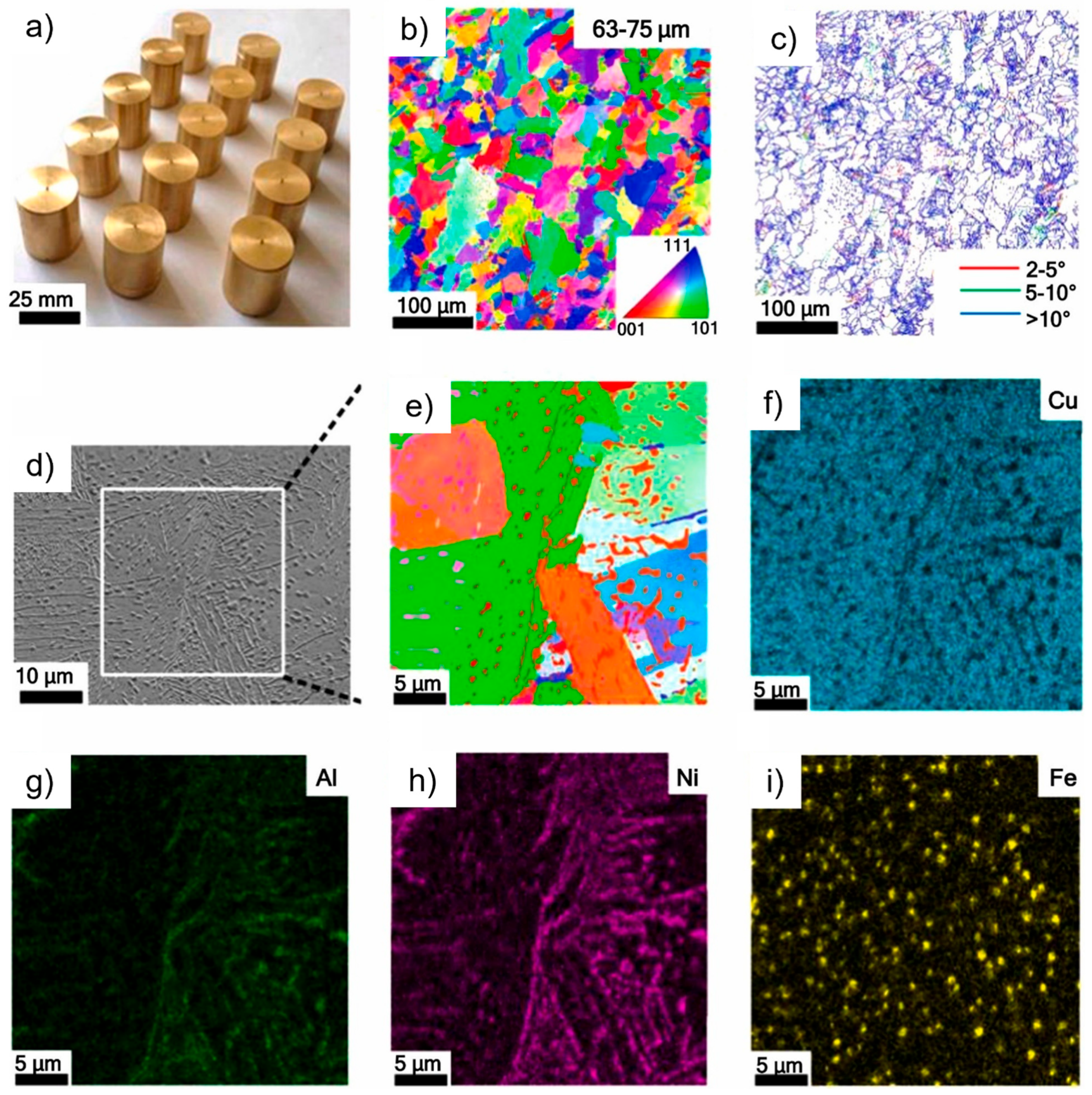
| L-PBF | NAB alloys C63000 (Cu-10.2Al-4.8Fe-5.0Ni-0.2Si) and C95800 (Cu-9.0Al-4.0Fe-4.6Ni-1.9Mn) |
| [163] |
| L-PBF | Cu-9Al-4Fe-3Ni | Post-heating at:
| [164] |
| L-PBF | C95800 NAB alloy (Cu-9.8Al-5.2Ni-4.6Fe-0.3 Mn) |
| [165] |
| EBM | C63000 NAB alloy (Cu-9.5Al-4.2Ni-4Fe-1.2 Mn) | [166] | |
| EBM | (Fe, Ni)Al-reinforced NAB alloy (81.1Cu- 9.5Al-4.2Ni-4.0Fe-1.2Mn) | [167] | |
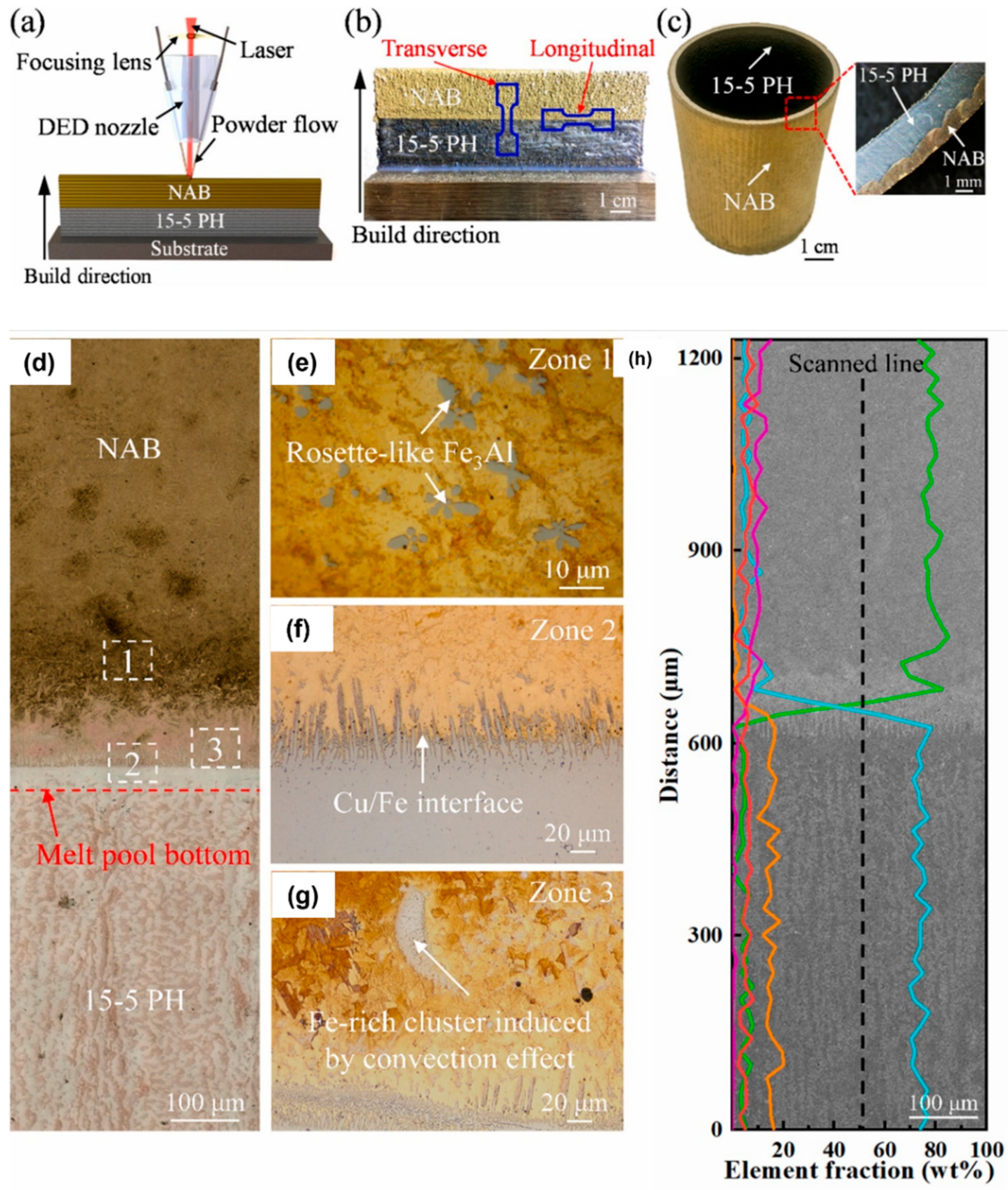
| L-DED | Bimetal: NAB on 15-5 PH stainless steel | [168] | |
| L-DED | Bimetal: CuNi2SiCr alloy layered on a cast AlBC3 NAB alloy | [169] | |
| L-DED | Bimetal: CuNi2SiCr alloy layered on a cast AlBC3 NAB alloy | [170] | |
| L-DED | Cu-9Al-5Fe-5Ni | [171] |


5.1. WAAM of NAB Alloys
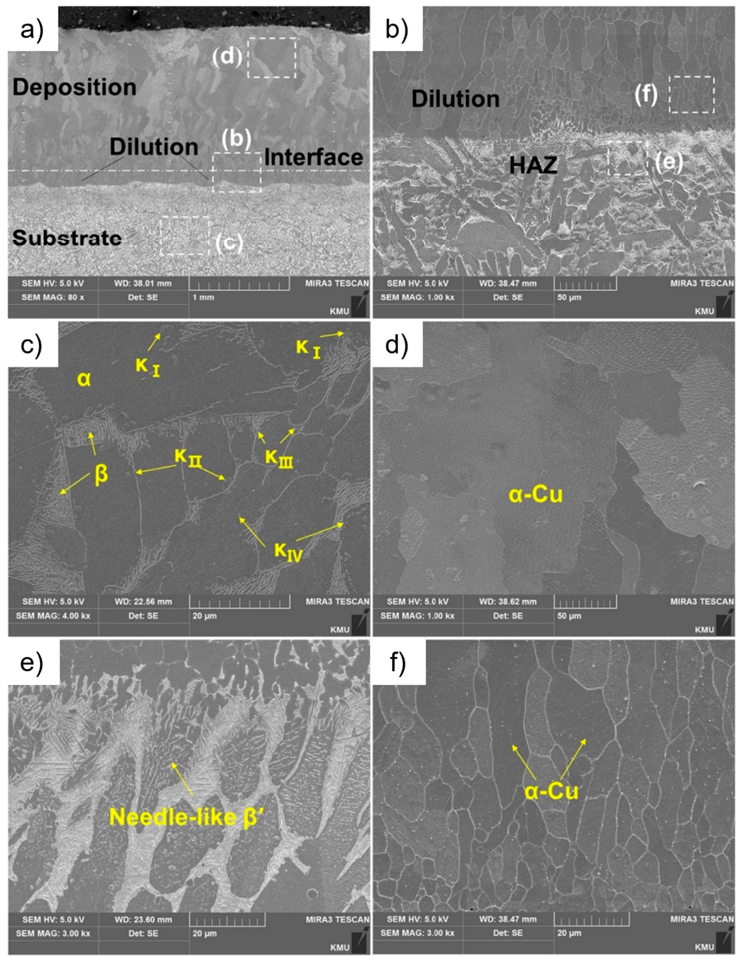
5.1.1. Microstructure of WAAM-Produced NAB Alloys
5.1.2. Mechanical Properties of WAAM-Fabricated NAB Alloys
5.2. L-PBF of NAB Alloys
5.3. EBM of NAB Alloys
5.4. L-DED of NAB Alloys
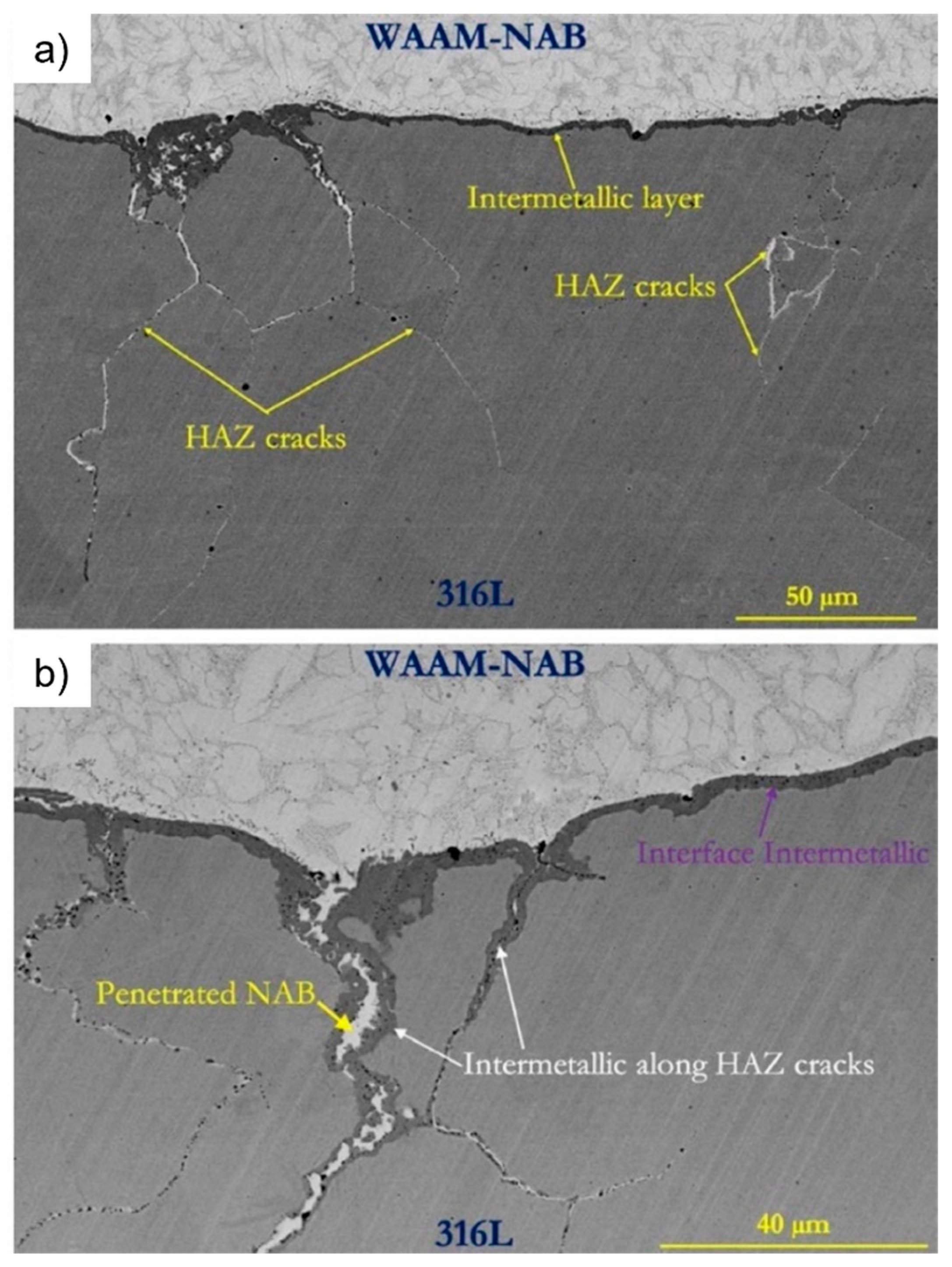
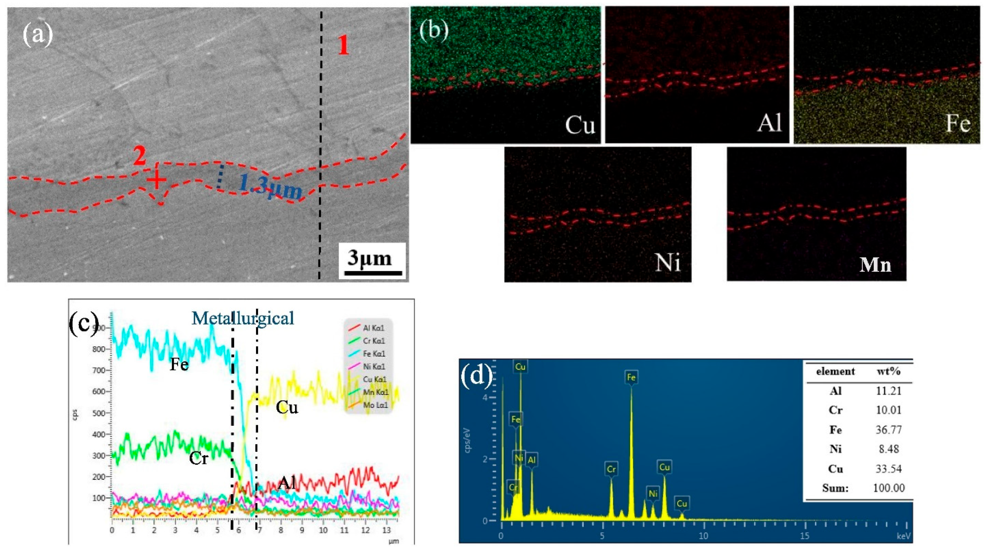
5.5. AM of Bimetallic NAB Alloys and Dissimilar Metal Combinations
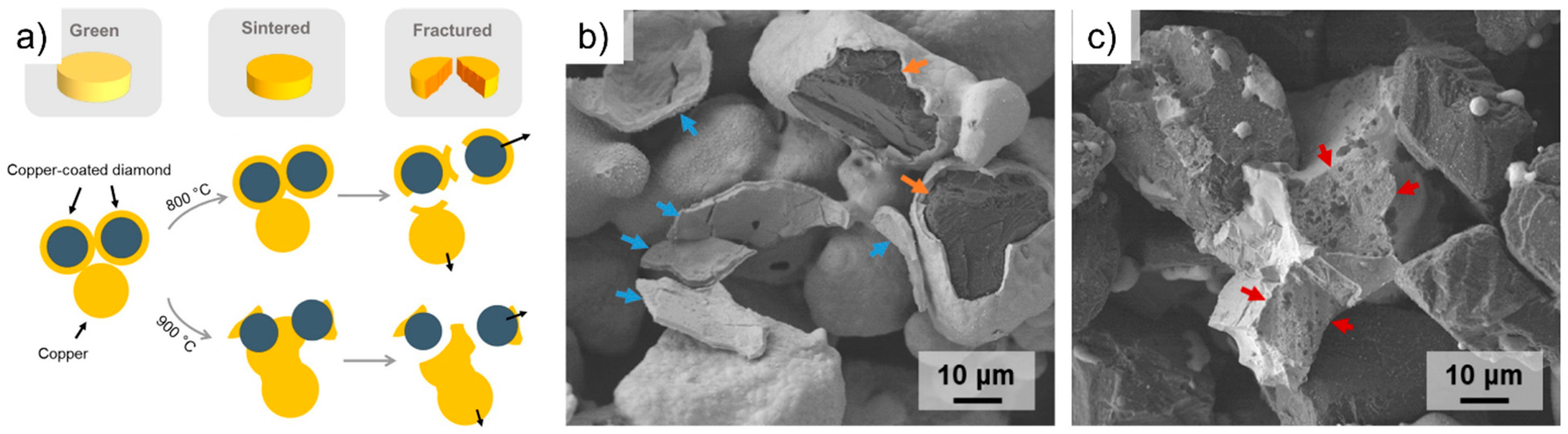
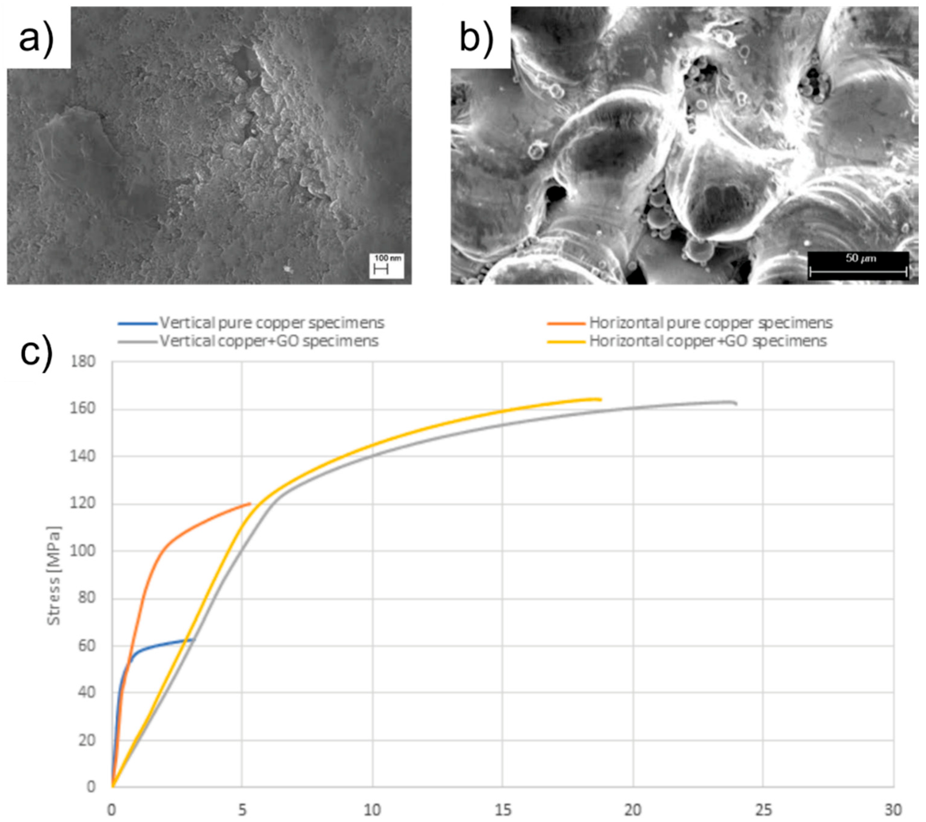
6. AM of Reinforced Copper Composites
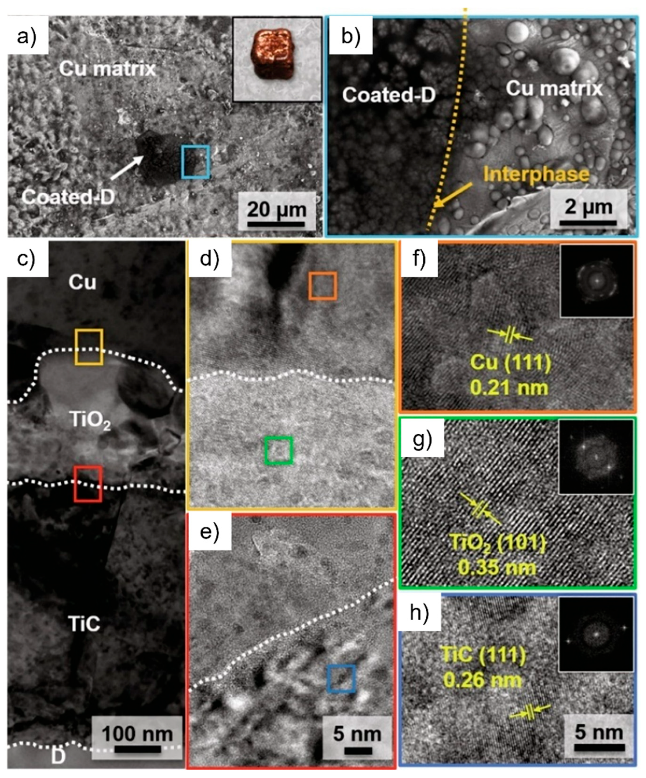
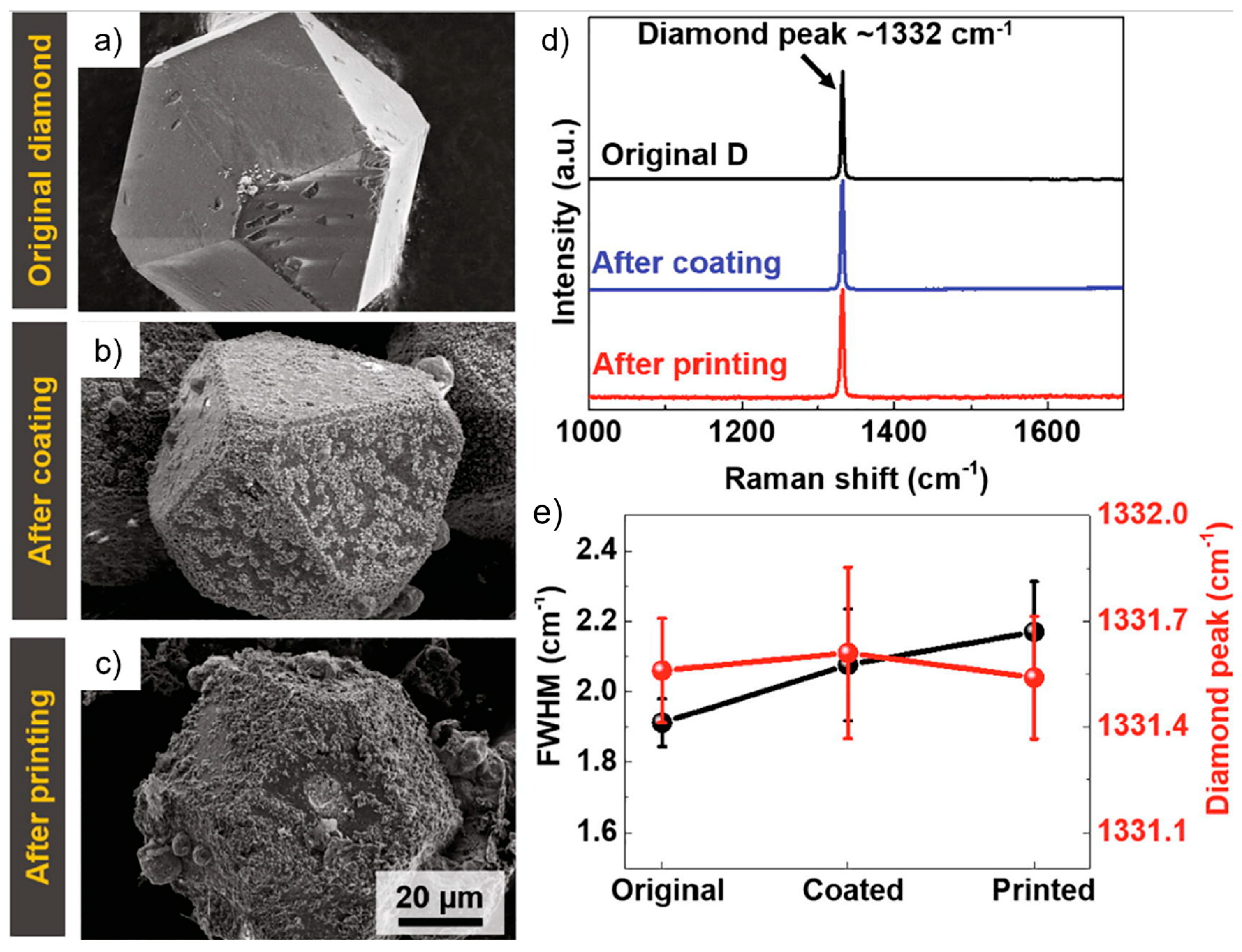
6.1. AM of Cu-C Composites
6.2. AM of Cu-Ceramic Composites
6.3. AM of Cu-Metal Composites
7. Future Perspective
- (i)
- Copper-chrome alloys: Future research should systematically investigate the corrosion behavior of additively manufactured copper-chrome alloys. Moreover, the in-service performance of EBM-fabricated copper-chrome alloys needs to be comprehensively studied to understand their potential for industrial applications.
- (ii)
- Copper-nickel alloys: Based on the present literature, the feasibility of manufacturing Cu-Ni alloys has been evaluated in a few studies, revealing anisotropic mechanical properties, microstructural inhomogeneities, and a relatively porous structure in the fabricated parts. To overcome these issues, future research should focus on optimizing the composition of the feedstock materials and production process parameters based on the specific applications of the intended end-products. A comprehensive study on the in-service performance and corrosion behavior of additively manufactured Cu-Ni alloys is also required.
- (iii)
- Tin-bronzes: While most of the available studies in the literature on tin-bronze alloys have focused on the L-PBF fabrication method, exploring the feasibility of arc-DED or WAAM, followed by process optimization, could provide a new opportunity for the production of large-scale tin-bronzes suitable for marine applications. Therefore, further research should be conducted on WAAM fabrication to determine its potential advantages and limitations for producing tin-bronzes.
- (iv)
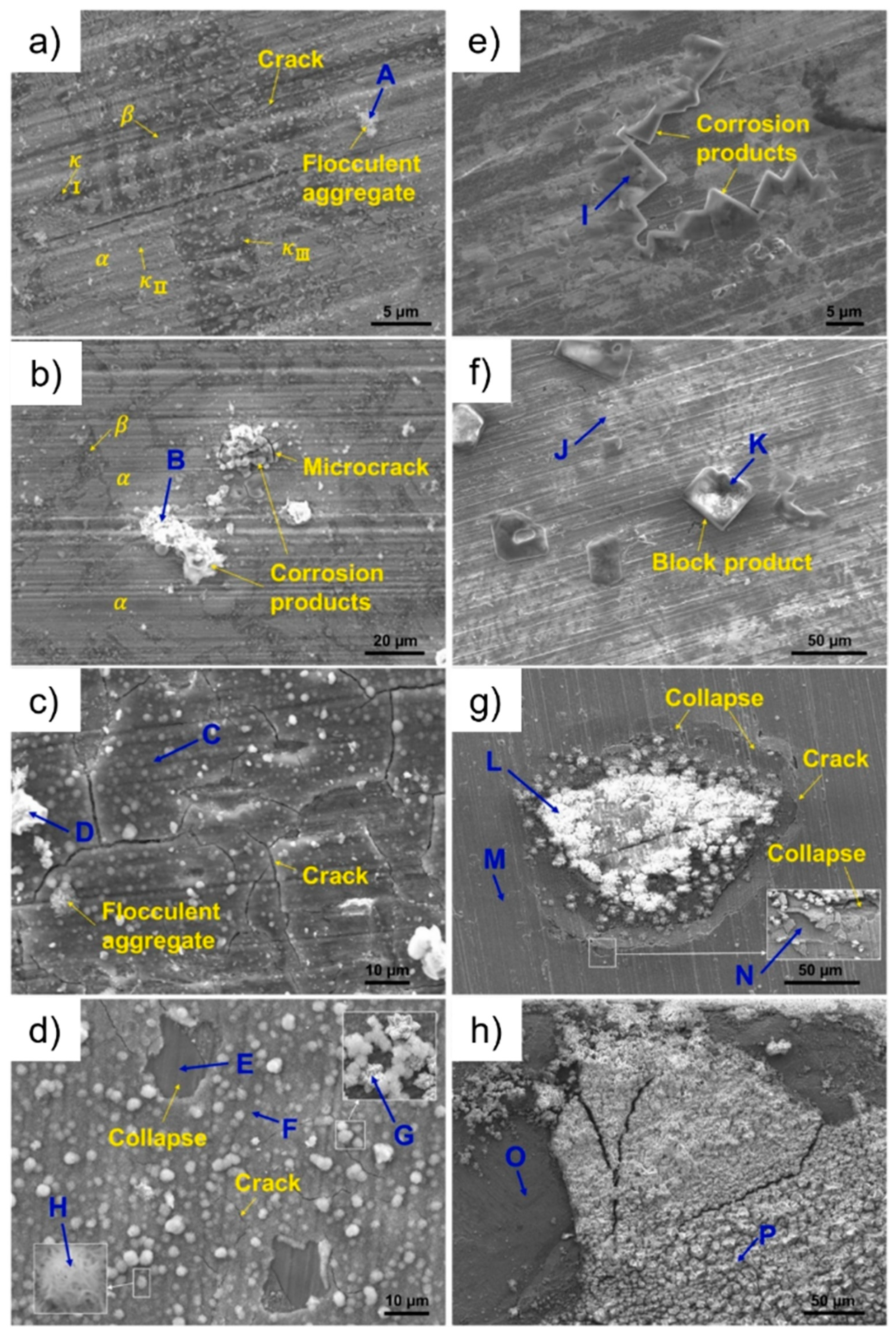
- NAB alloys: Future research is necessary to comprehensively investigate the seawater corrosion performance of AM-fabricated NAB alloys in both as-printed and heat-treated conditions, followed by comparison with the corrosion properties of their conventionally fabricated counterparts. Since NAB alloys are widely used in the marine industry, these studies could have significant practical applications.
- (v)
- Reinforced copper composites: As most of the existing research on these materials is in the feasibility stage, there is a significant potential for future studies focused on optimizing the process parameters for additive manufacturing of MMCs. This can be followed by an investigation of the resulting physical and mechanical properties. Such studies could lead to a better understanding of the behavior of these materials and open up new possibilities for their industrial applications.
8. Summary and Conclusions
- The processability of copper-based materials using L-PBF presents several challenges due to: (i) the high laser reflectivity of copper, which can damage the optical coating on the laser mirror; (ii) the high thermal conductivity of copper, which leads to a rapid heat transfer from the melt pool region to the surrounding area, causing layer curling and delamination in the as-printed material due to a significant local temperature gradient; (iii) the low laser energy absorptance rate of copper, leading to a porous as-printed part; and (iv) the rapid oxidation of copper feedstock powders during processing, leading to gas bubbles entrapped in the end-product as porosities. To address these challenges, the following solutions are suggested: (i) adopting a high-power laser, (ii) preheating the powder bed, (iii) using laser sources with lower wavelengths, (iv) employing a lower conductive material for the building platform, and (v) incorporating alloying elements or composite particles into the material.
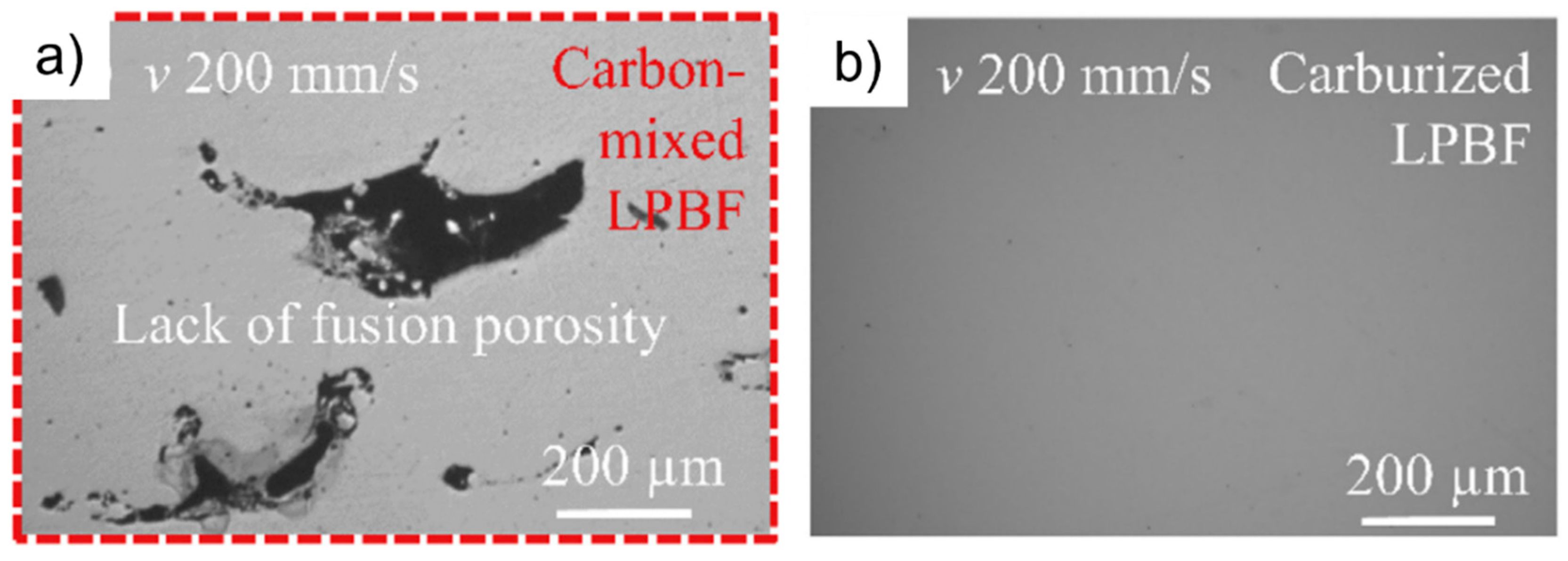
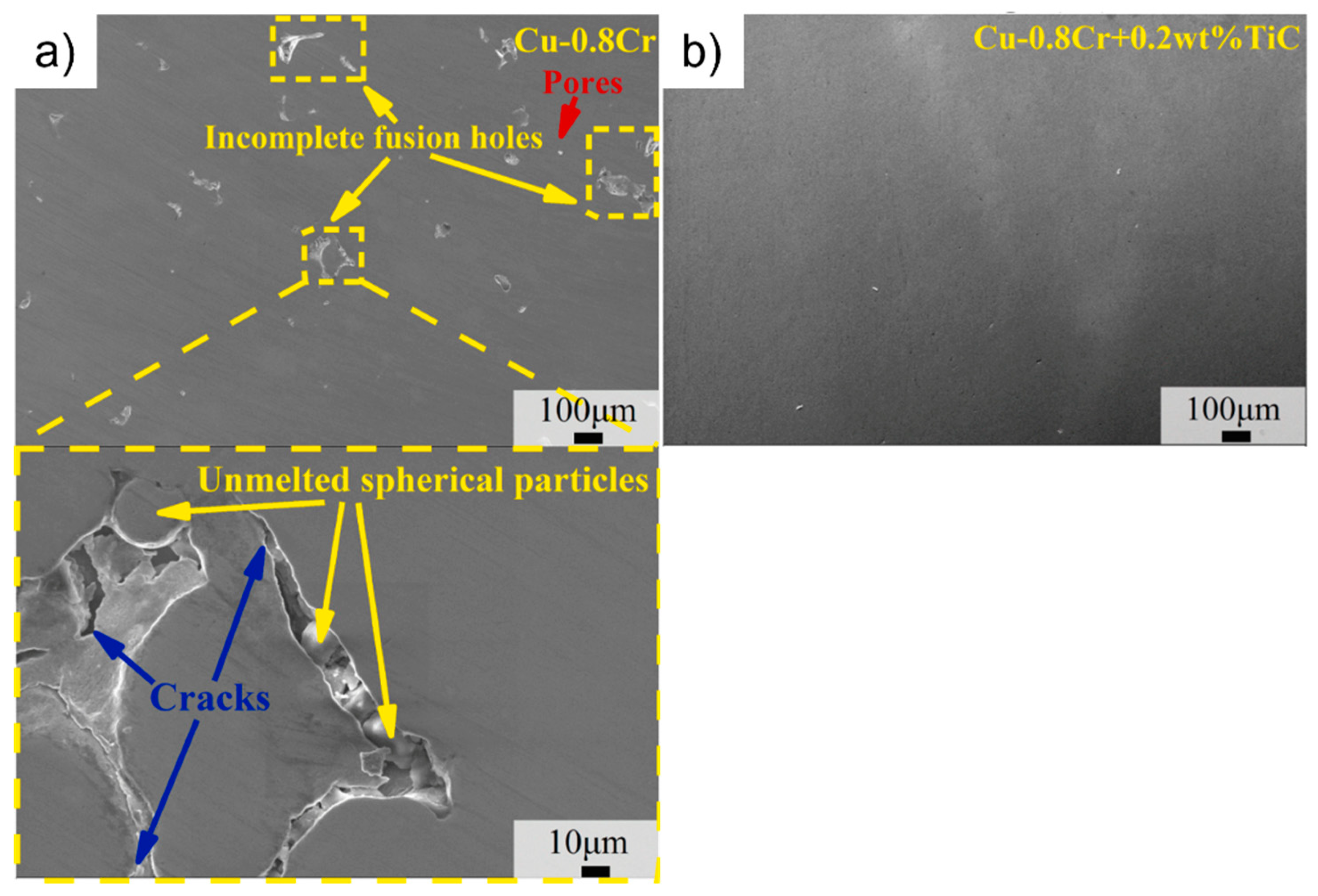
- The addition of alloying elements to pure copper can deteriorate its electrical and thermal conductivities. Therefore, developing copper-based MMCs can be an effective way to overcome the L-PBF processability challenges of copper-based materials and produce tailored-to-design parts. While most of the available studies in the literature have focused on employing carbon-based particles as reinforcements, it is important to consider the avoidance of in-situ graphitization during the AM process.
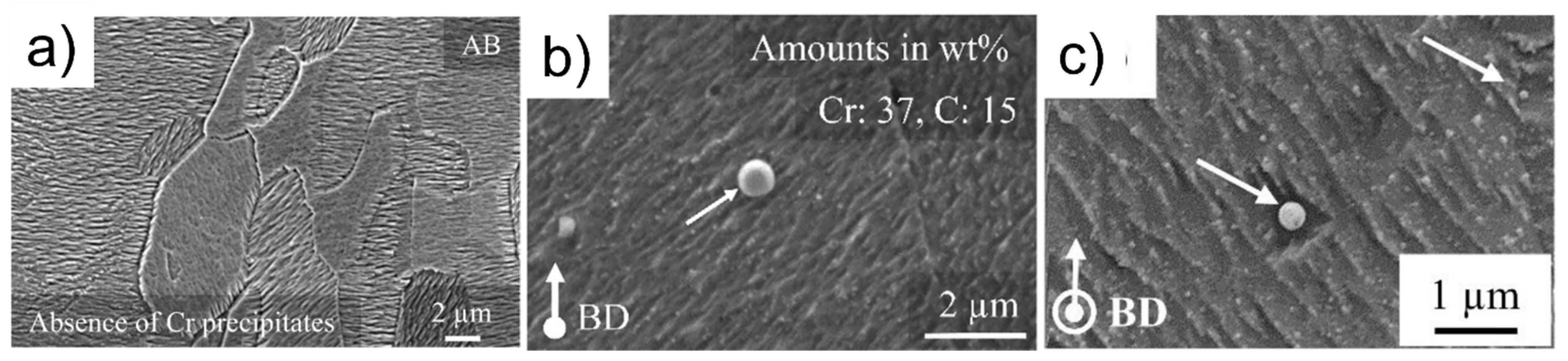
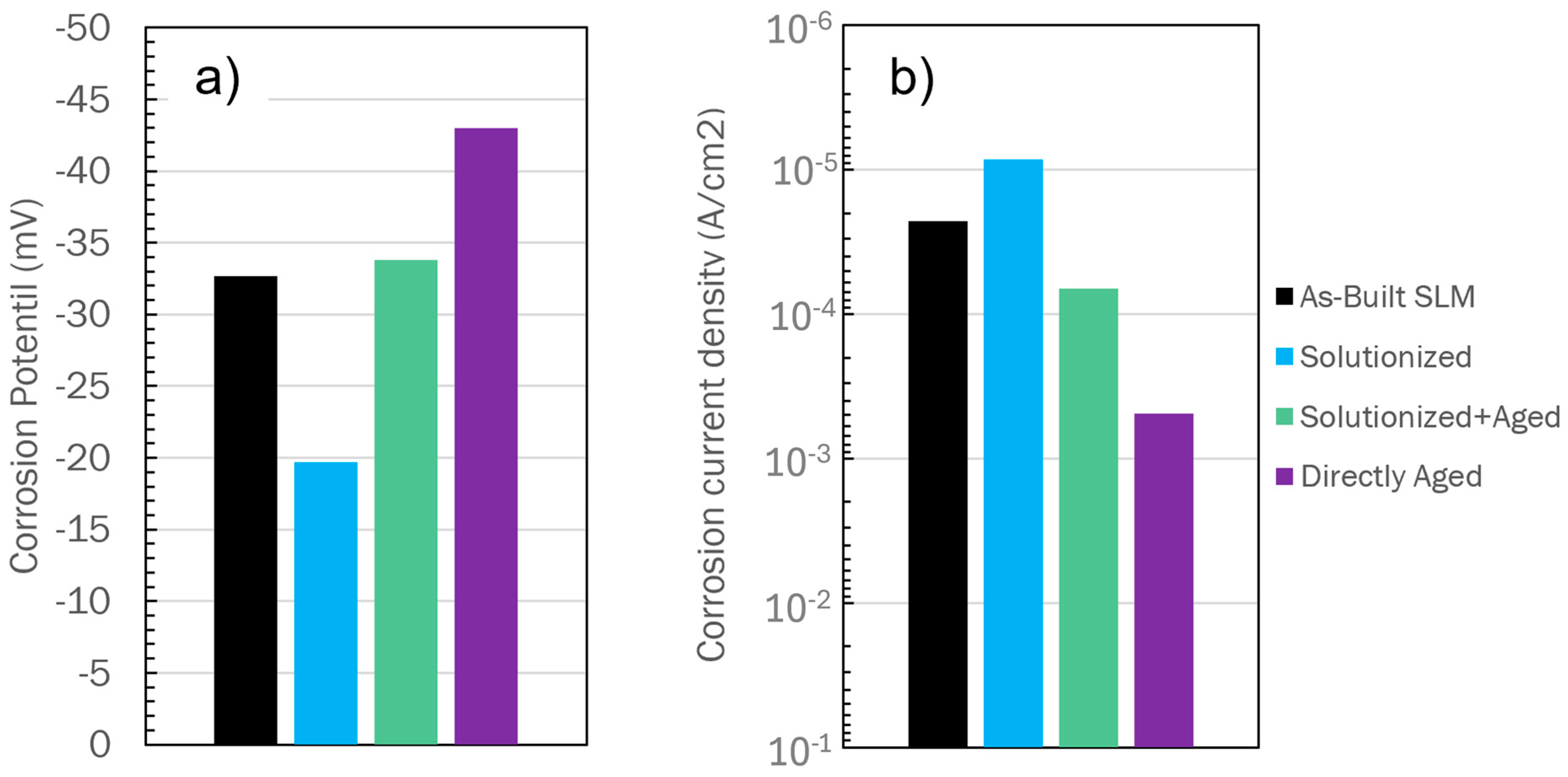
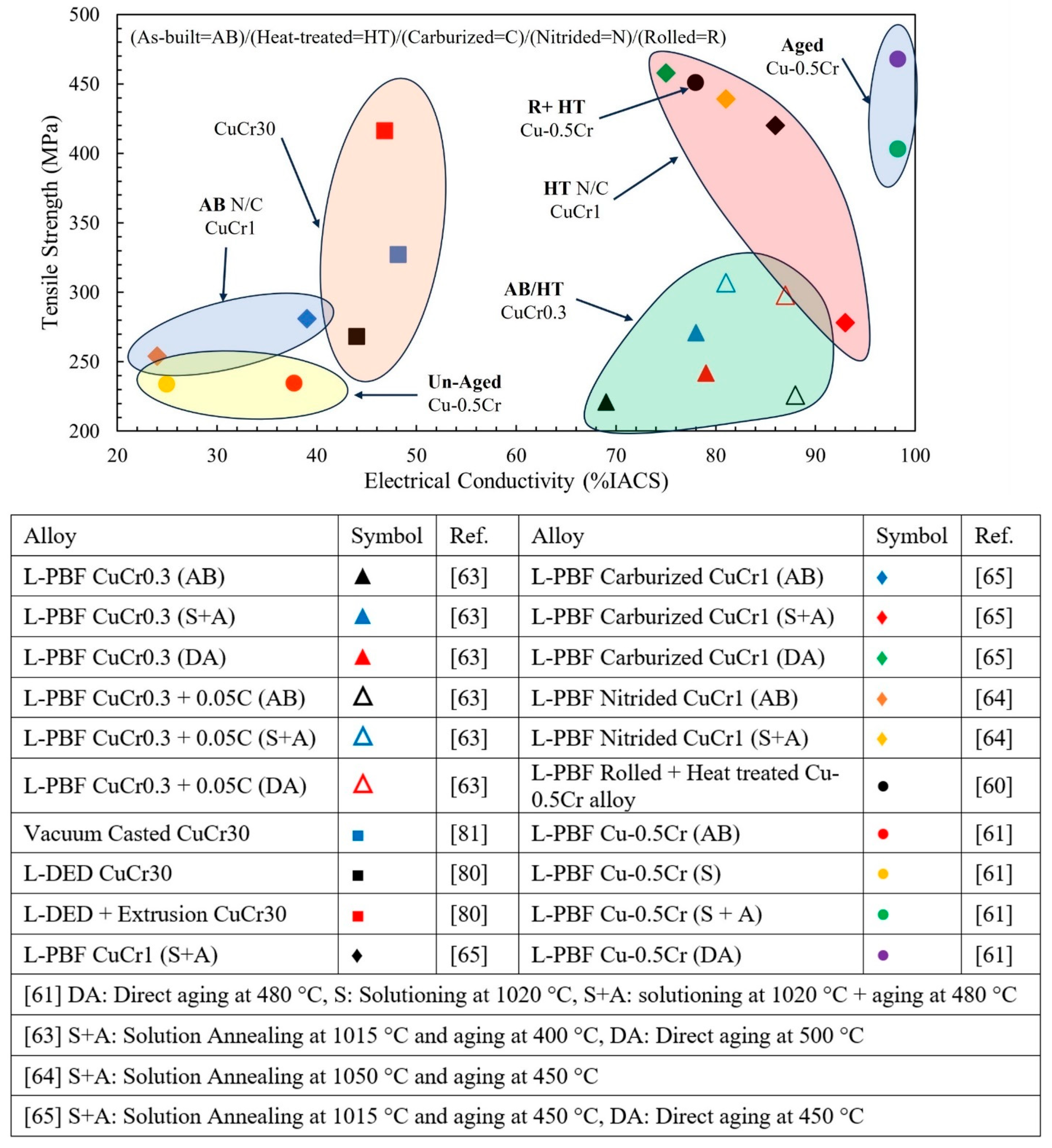
- In the case of copper-chrome alloys, the high solidification rate associated with AM is advantageous in preventing the segregation of chrome, which is a common issue during traditional manufacturing methods of copper-chrome alloys such as casting. This results in AM-processed components with superior mechanical properties compared to their conventionally produced counterparts. However, post-printing processes, such as mechanical deformation or heat treatment, are required to balance the properties of additively manufactured copper-chrome parts. It is important to optimize the post-printing heat treatment cycles to achieve the desired characteristics, as the ideal microstructure is obtained at a threshold temperature that may differ from the recommended heat treatment cycles for conventionally fabricated copper-chrome counterparts. Specifically, conventionally fabricated copper-chrome parts yield the optimum properties with solution-aging heat treatment, while their additively manufactured counterparts exhibit the best combination of strength and conductivity with direct aging.
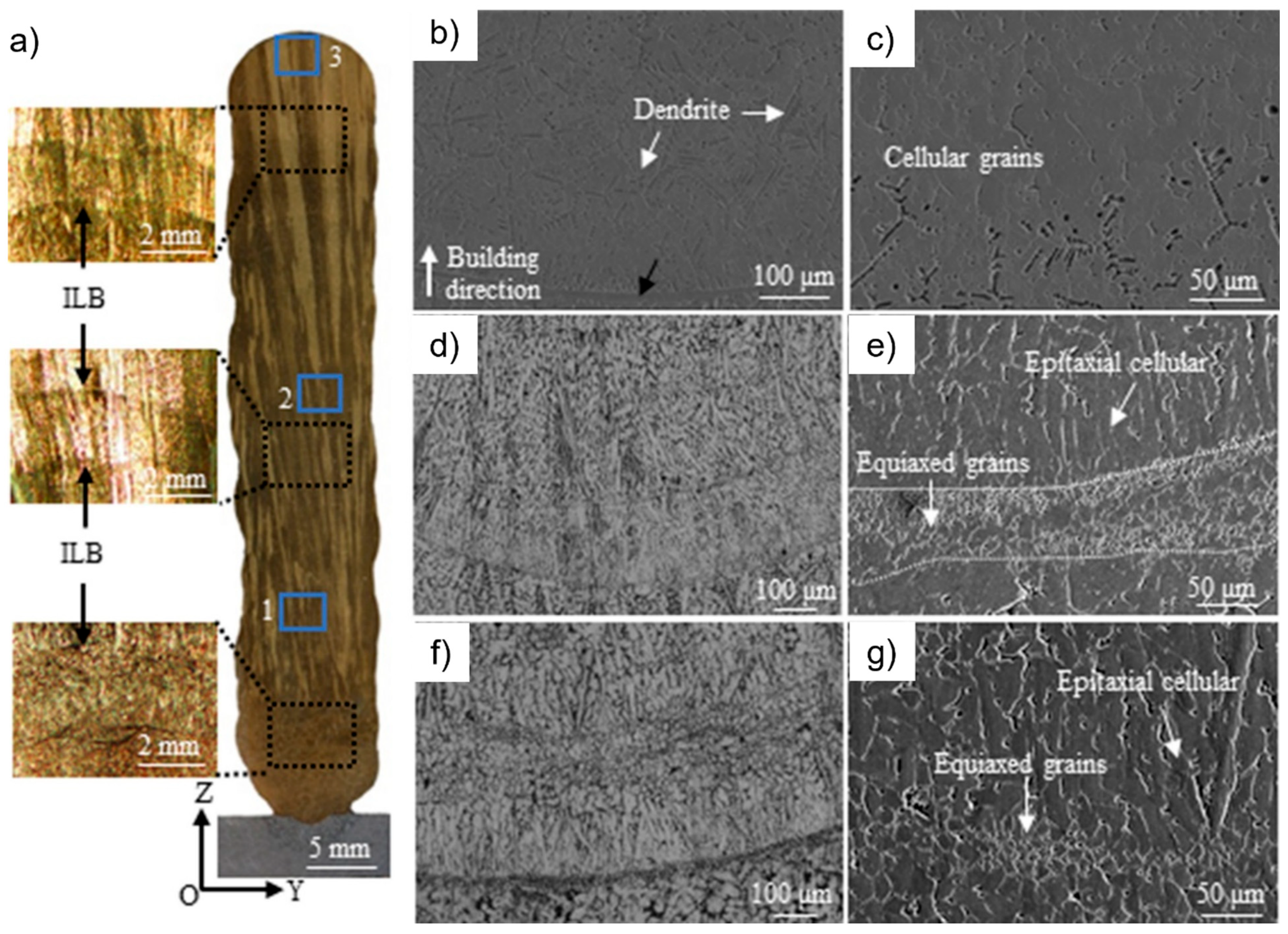
- In the case of copper-nickel alloys, the higher cooling rates associated with the L-PBF process suppress the recrystallization process, leading to the formation of a quasi-amorphous (metal glass) microstructure and higher hardness in as-printed parts compared to the conventionally fabricated parts in the annealed condition. Faster scanning and higher layer thickness increase the porosity level and decrease the corrosion resistance and hardness of the as-printed Cu-Ni alloys. However, adopting a higher scan speed during L-DED processing of Cu-Ni alloys has been found to be detrimental to the soundness of the deposited tracks, primarily due to insufficient laser energy absorption by the feedstock material. L-DED processing of Cu-Ni alloys results in a crystalline microstructure with a mix of cellular and dendritic structure at the bottom/middle layers and equiaxed grains at the top regions, in contrast to the quasi-amorphous structure obtained in L-PBF processed Cu-Ni alloys. Compared to beam-based AM processes, the WAAM process is more effective in producing sound and defect-free Cu-Ni alloys with negligible discontinuities and internal porosities. However, WAAM-fabricated Cu-Ni alloys may exhibit anisotropic mechanical properties due to different grain sizes and the presence/absence of precipitates in different orientations.
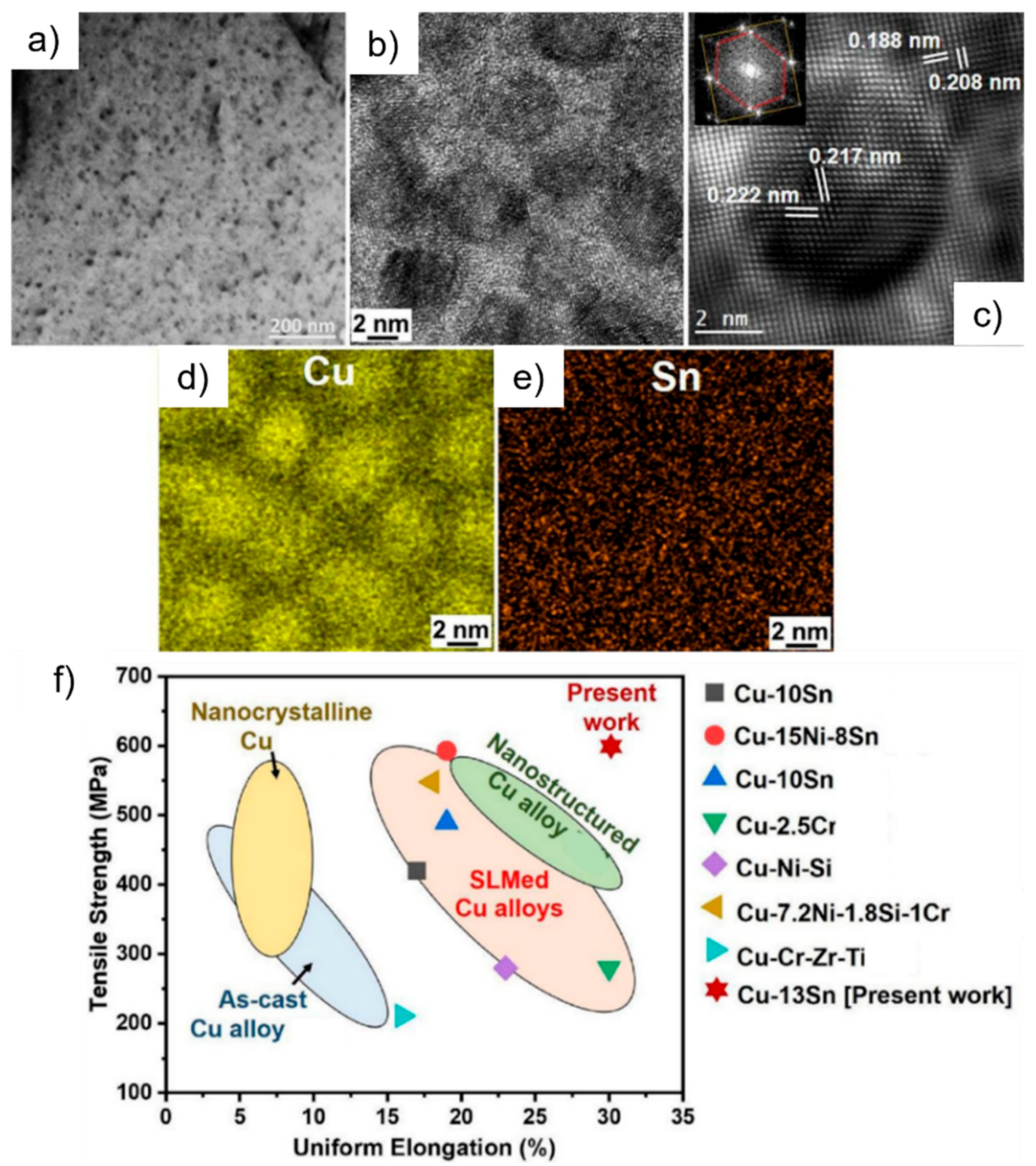
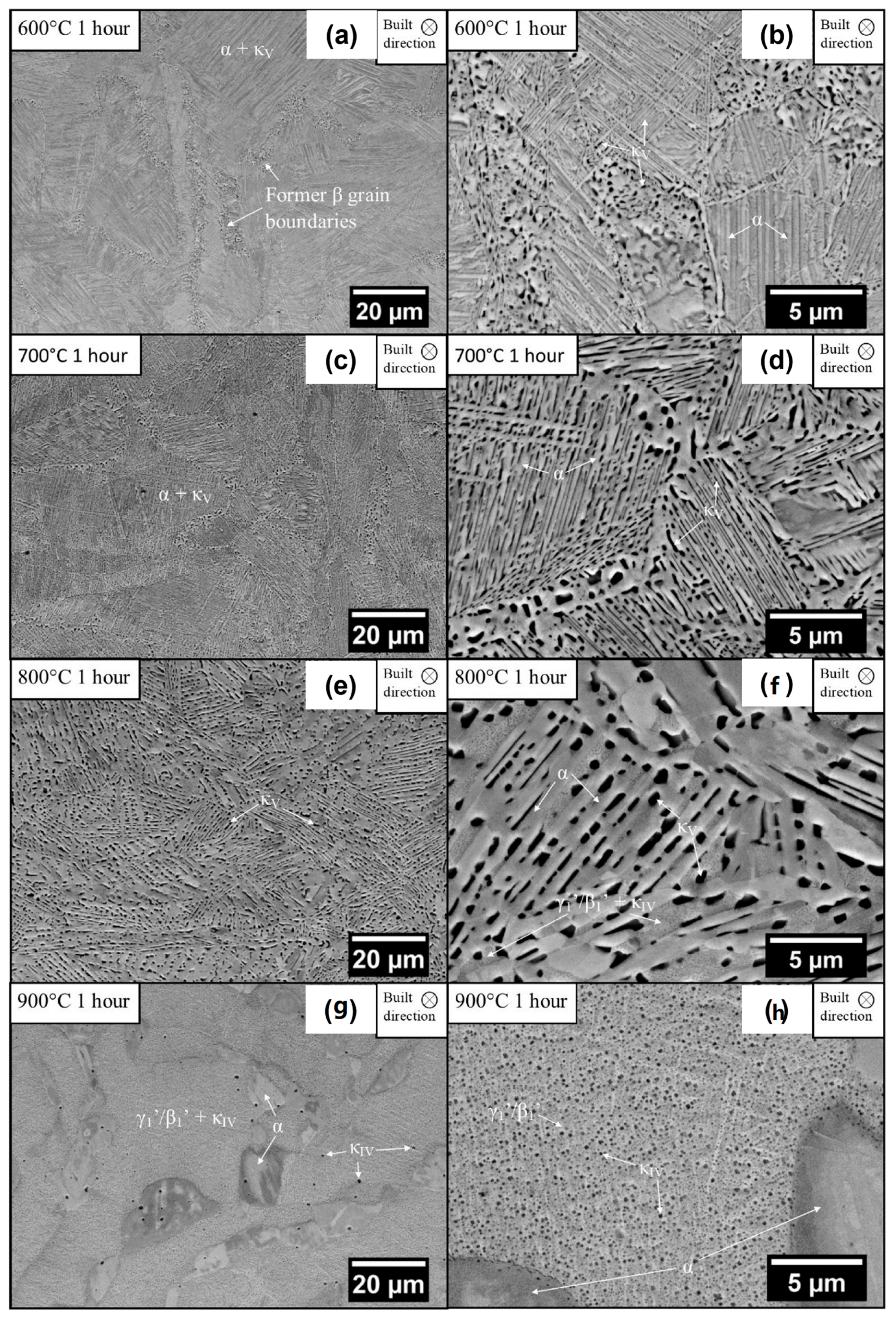
- Tin-bronzes fabricated using AM have a microstructure similar to those produced by traditional casting but with a finer microstructure due to the faster cooling rate associated with the AM process. Sequential melting and reheating cycles during AM lead to the formation of a low-volume fraction of ε secondary phases, which act as an artificial aging heat treatment cycle. The finer microstructure and presence of hard ε-precipitates in AM-fabricated tin-bronzes result in a better combination of strength and ductility compared to cast samples. However, the post-fabrication annealing process can eliminate the heterogeneous microstructure and consequently alter the mechanical response, thermal properties, and corrosion resistance of AM-fabricated Cu-Sn alloys. In particular, the annealing process results in the formation of a coarse single-phase microstructure, improving ductility and corrosion resistance, but at the cost of reduced mechanical strength.
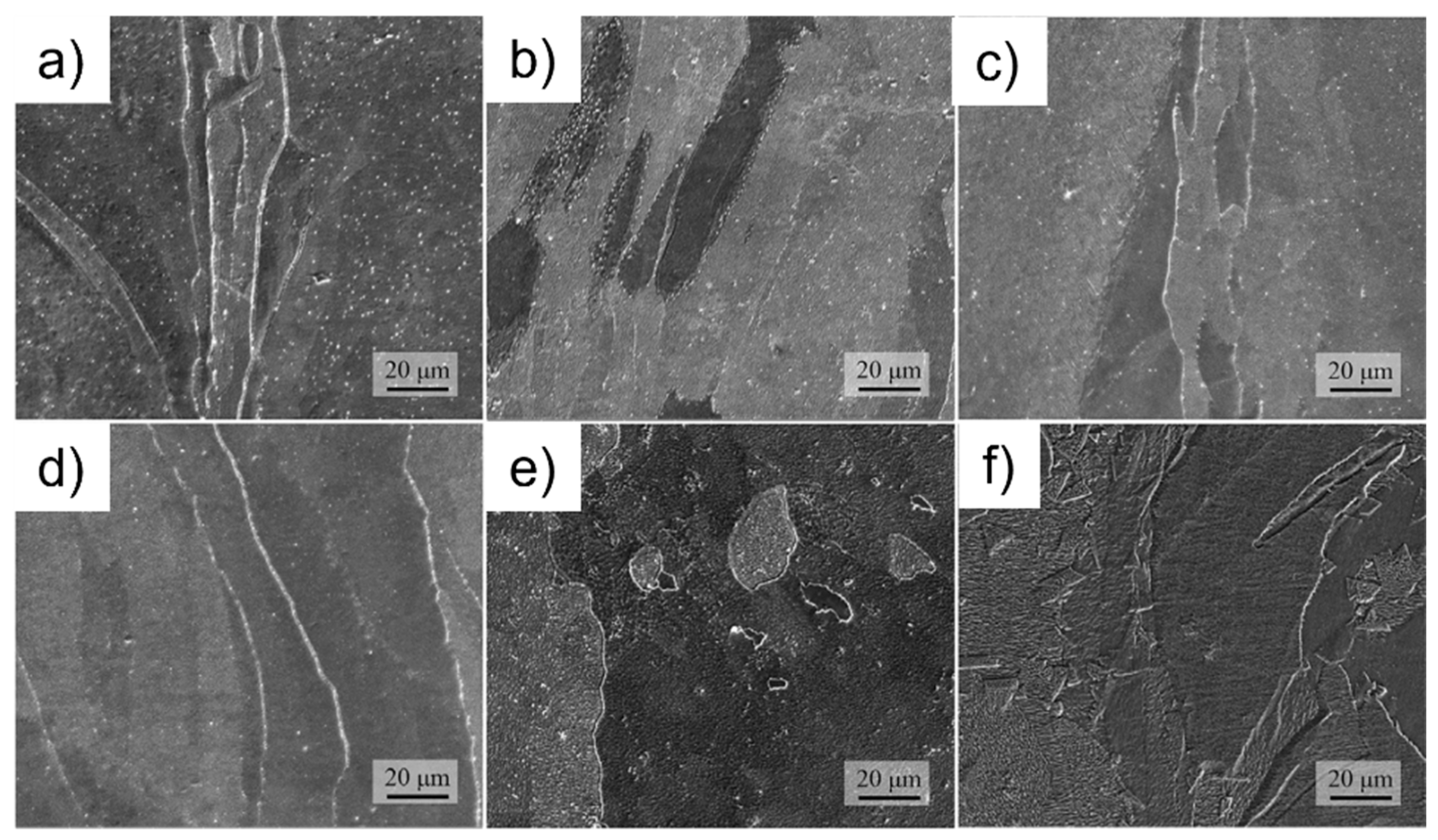
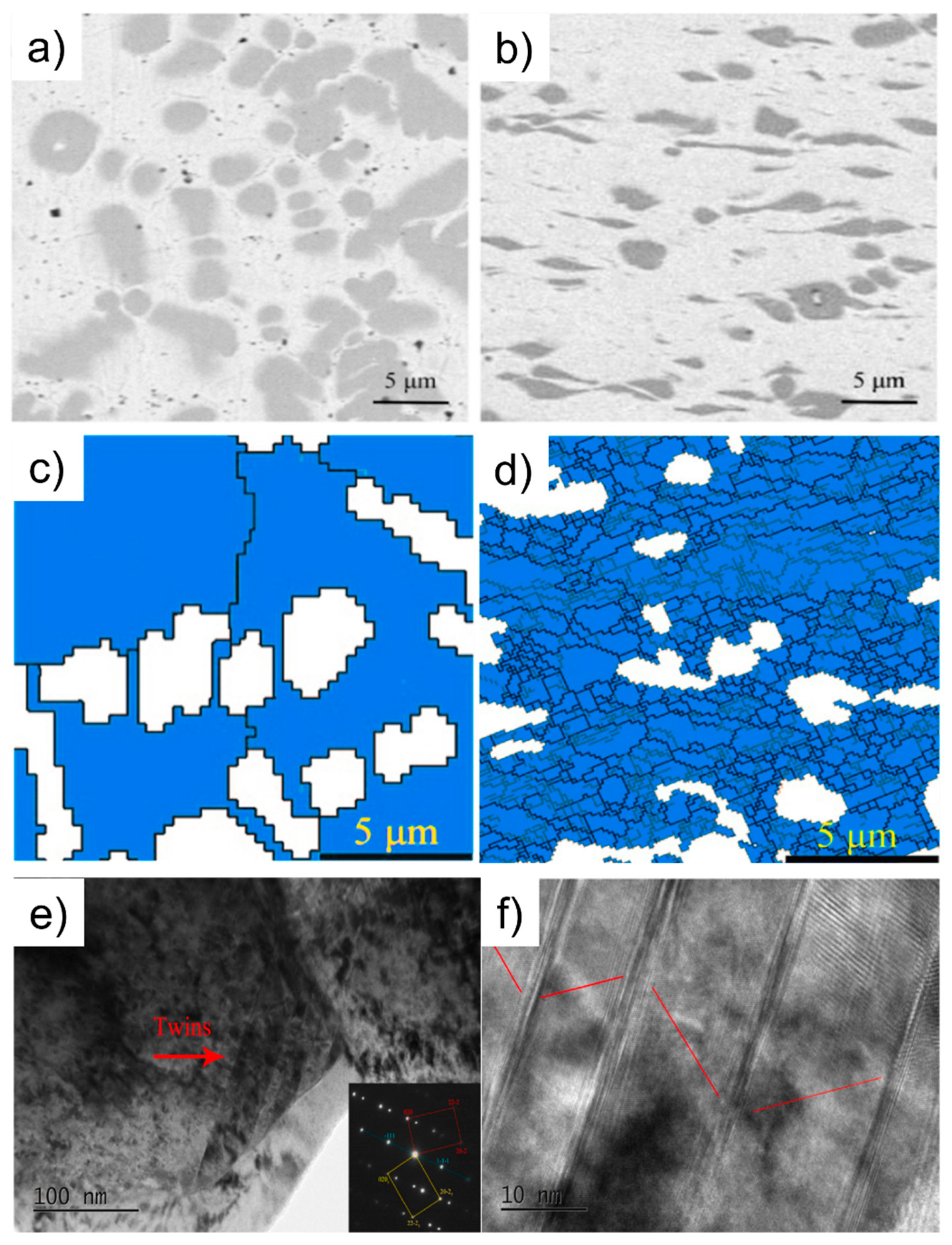
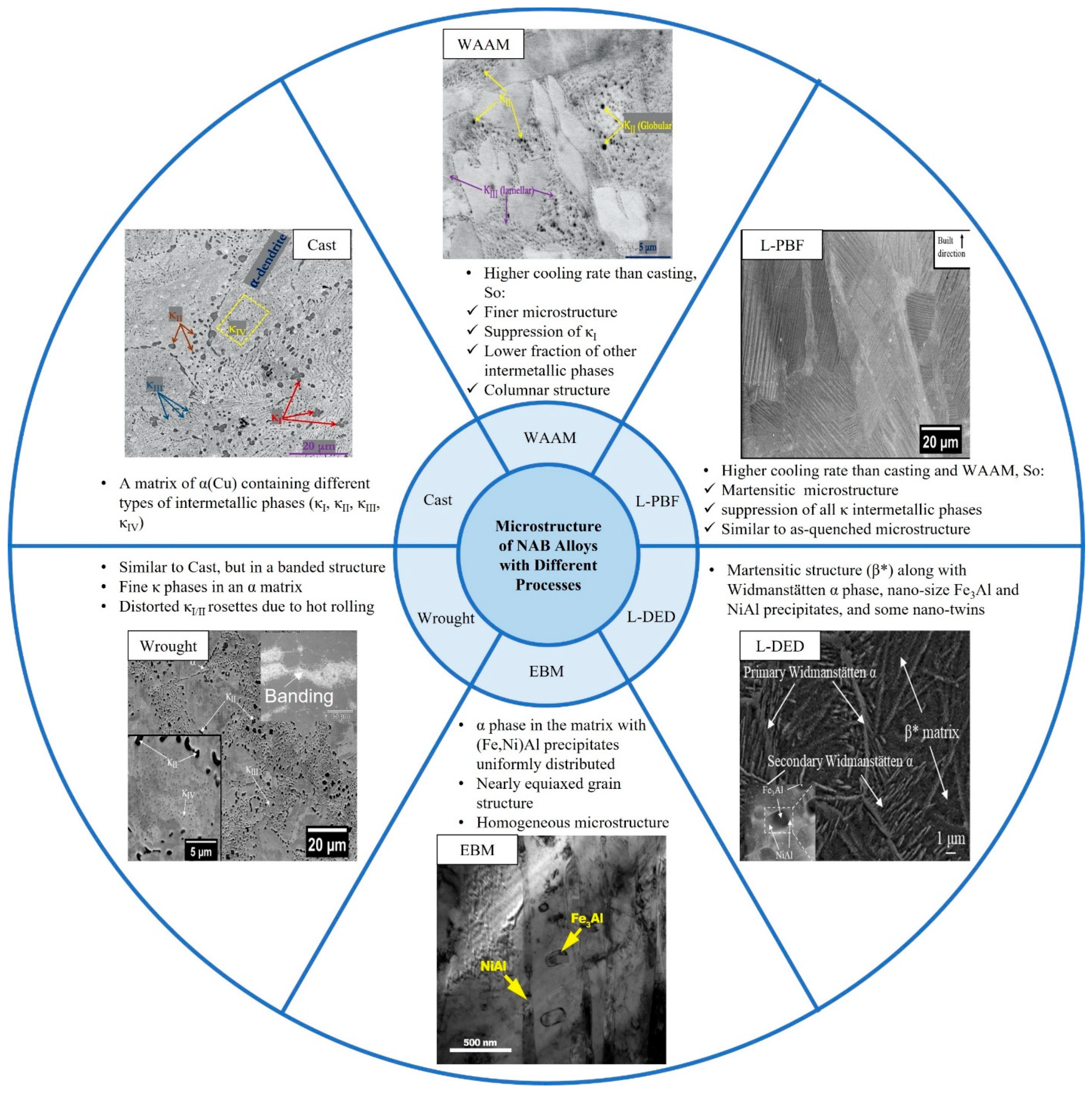
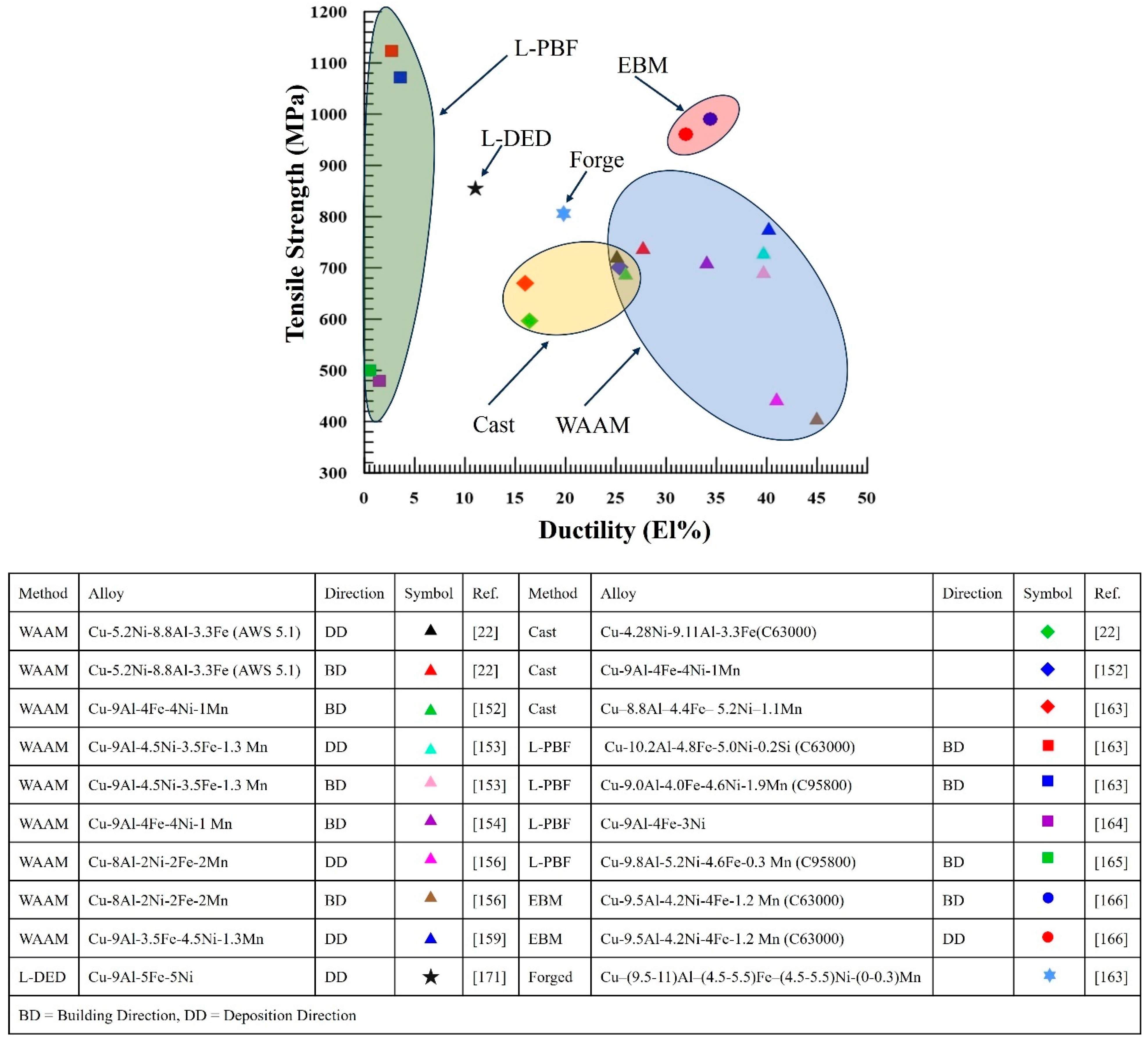
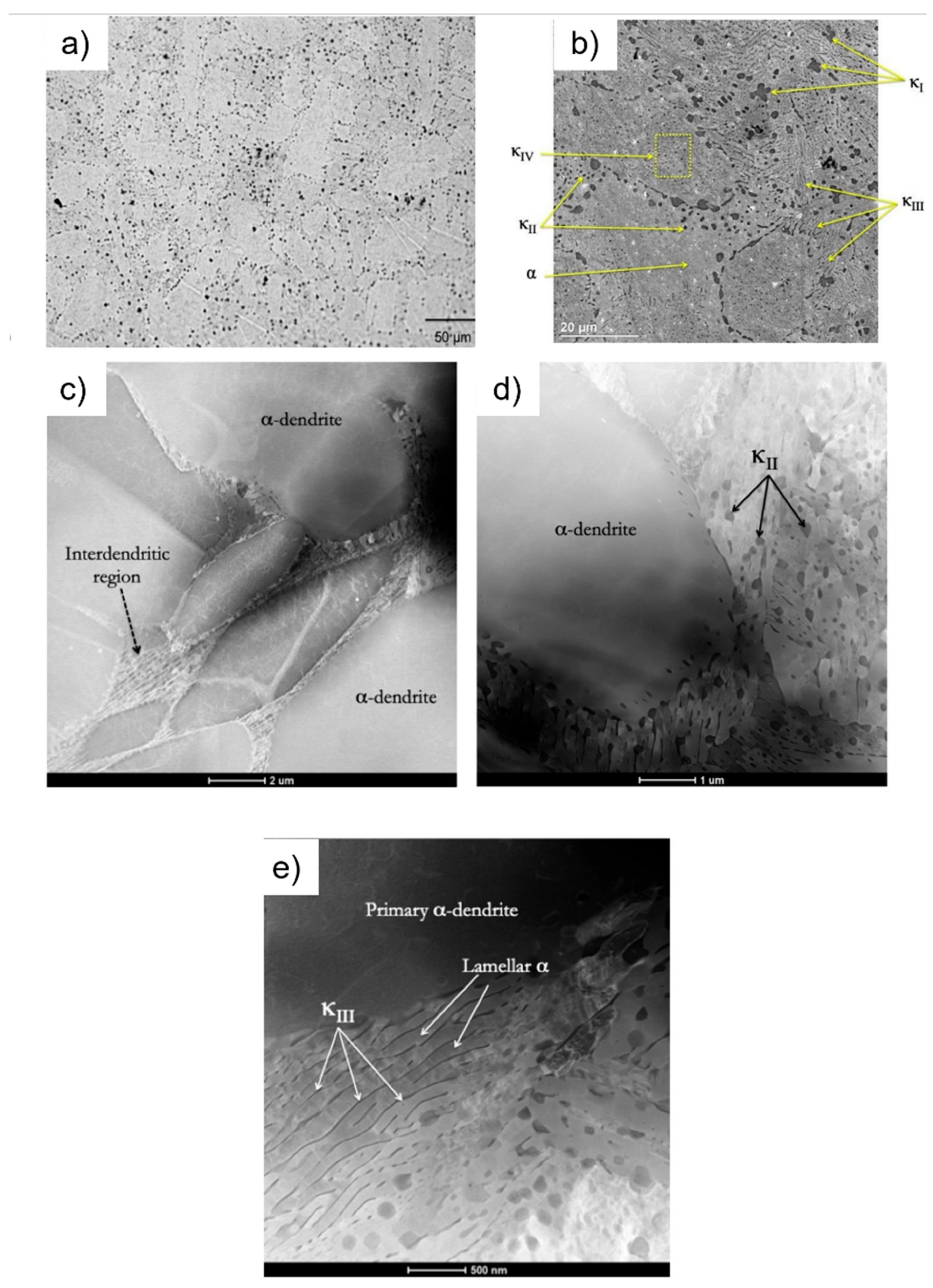
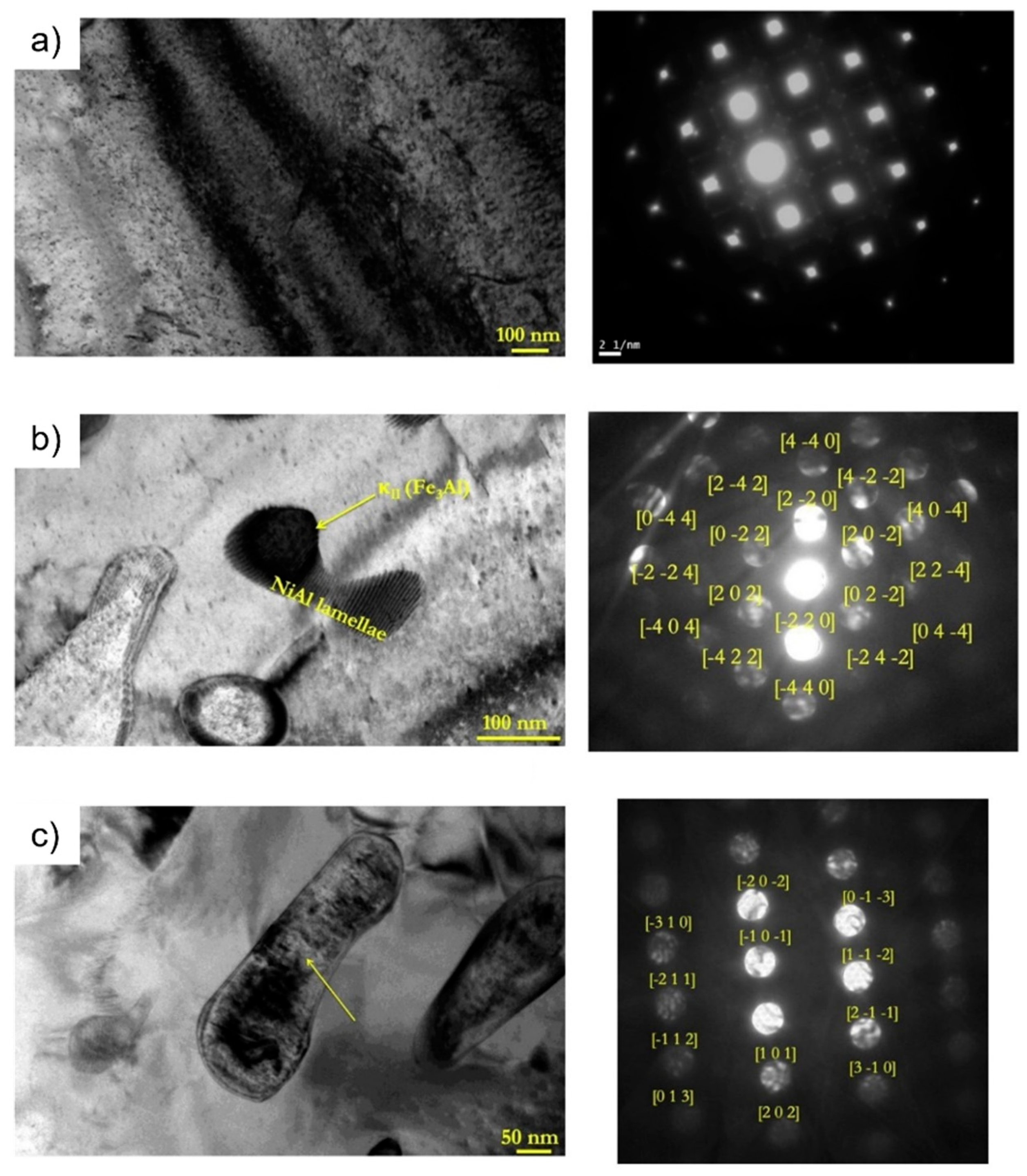
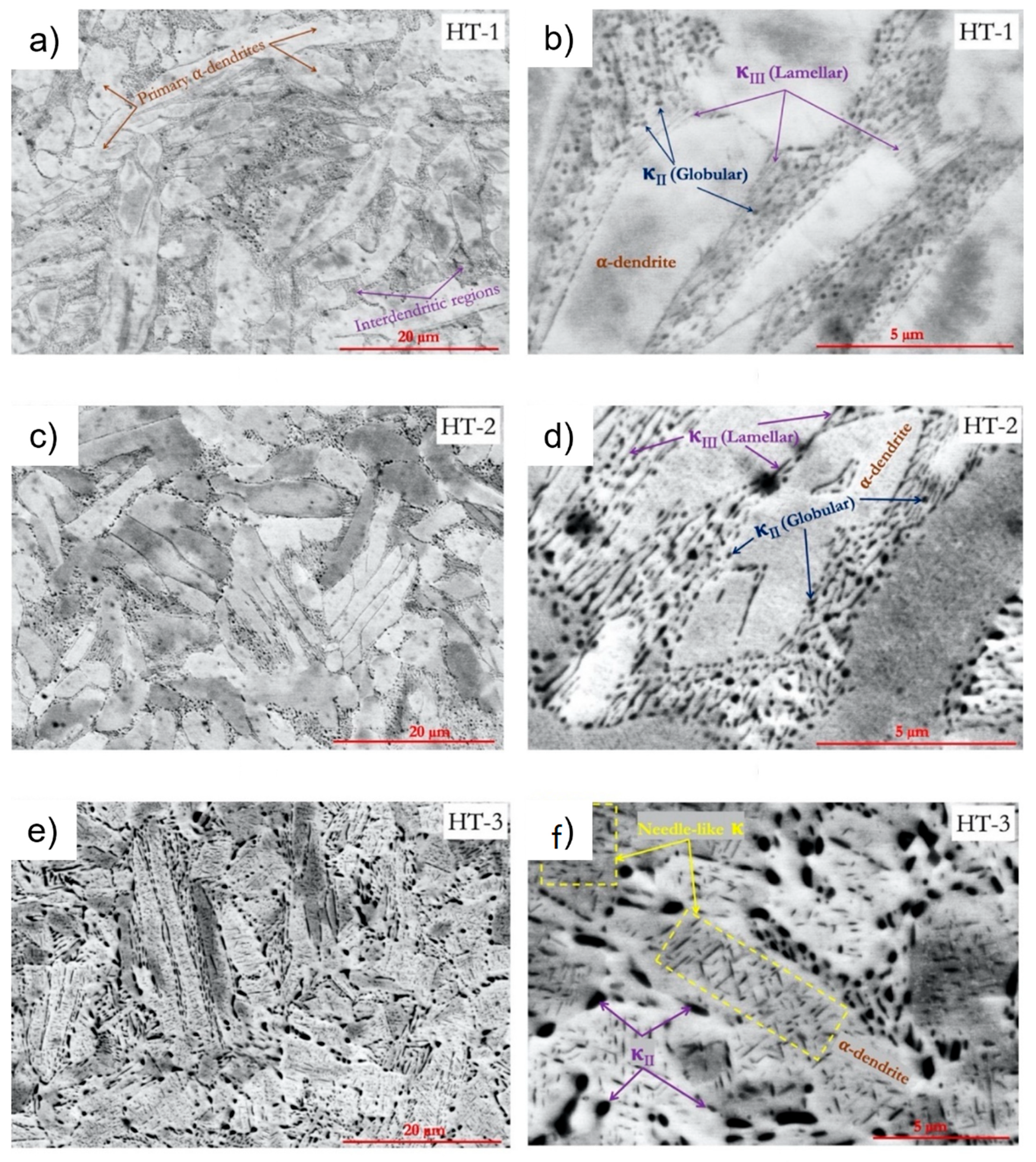
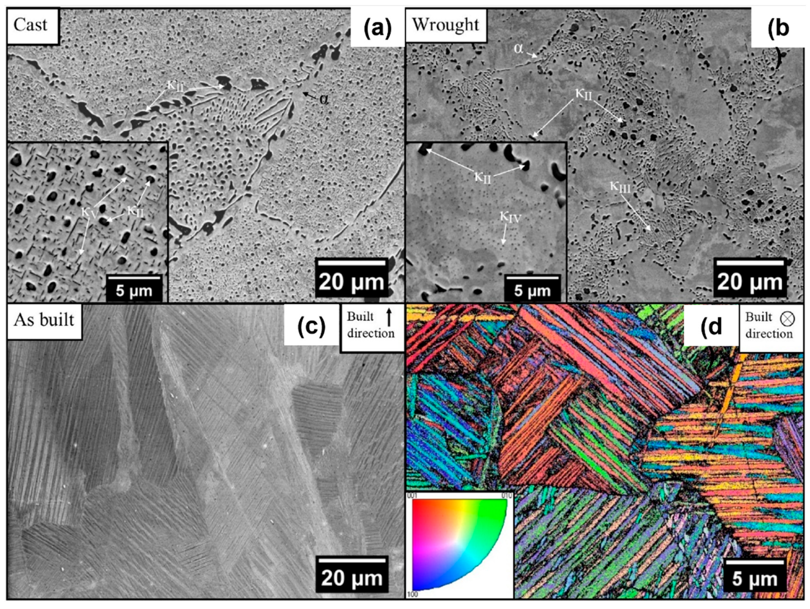
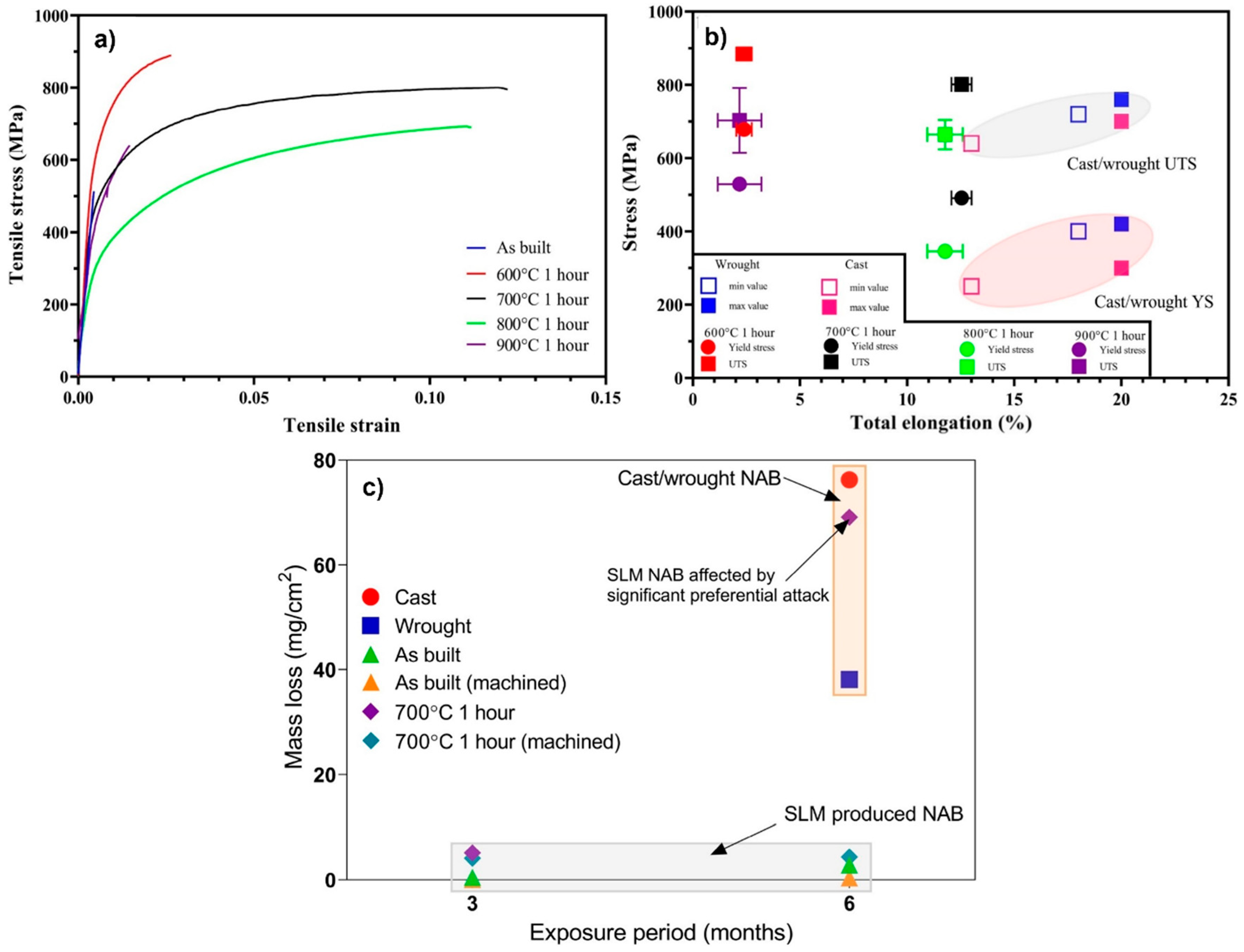
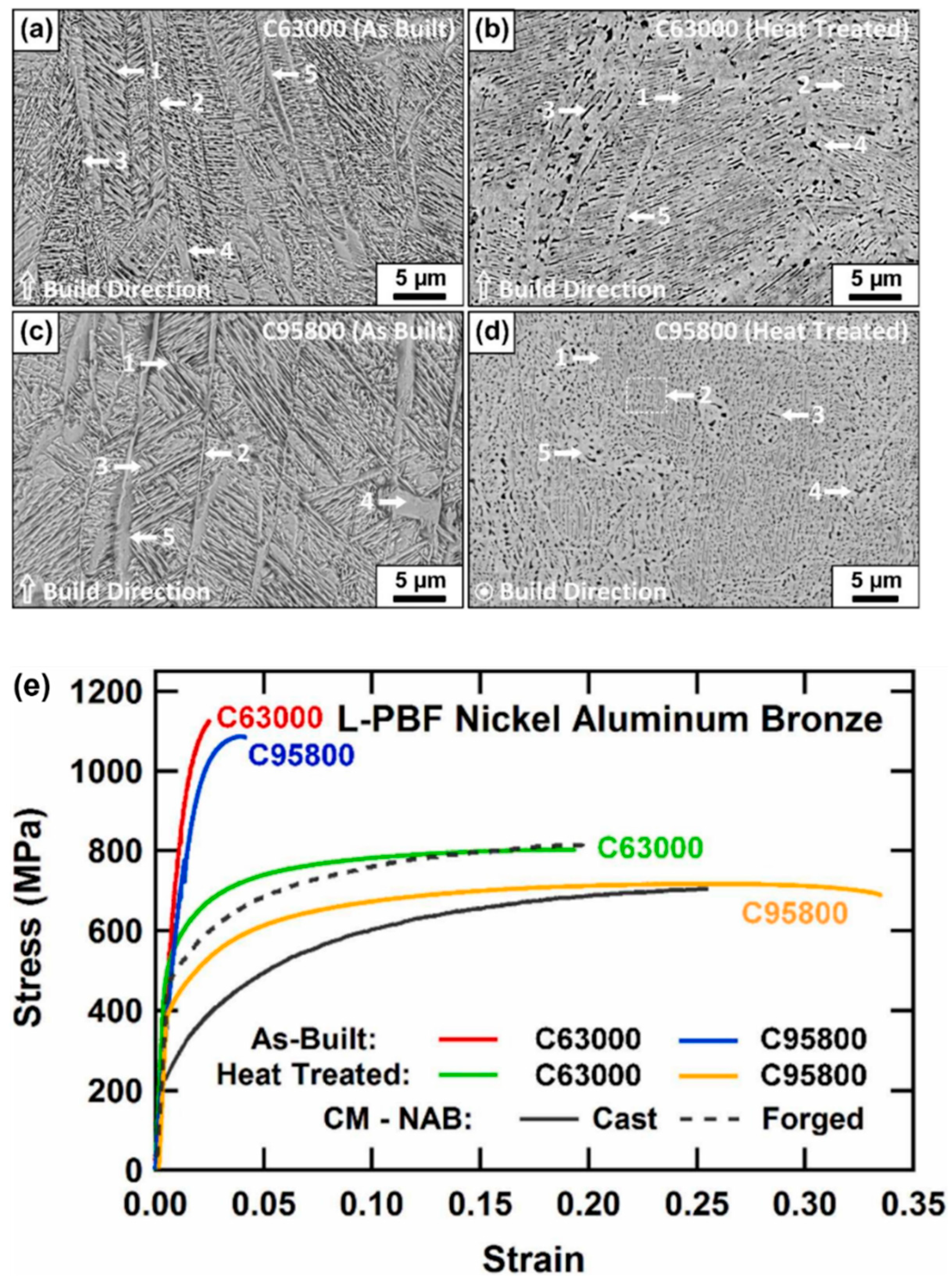
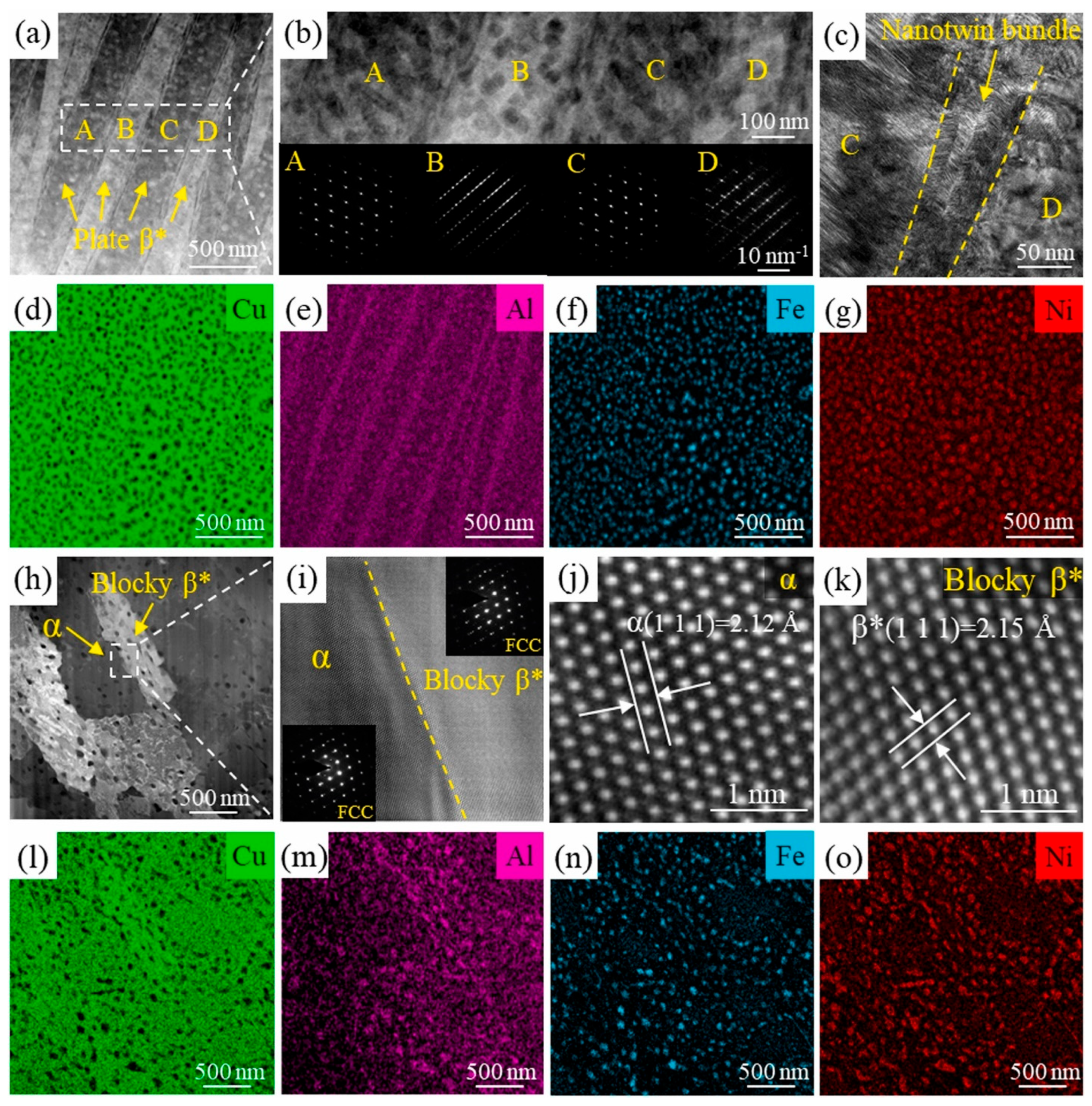
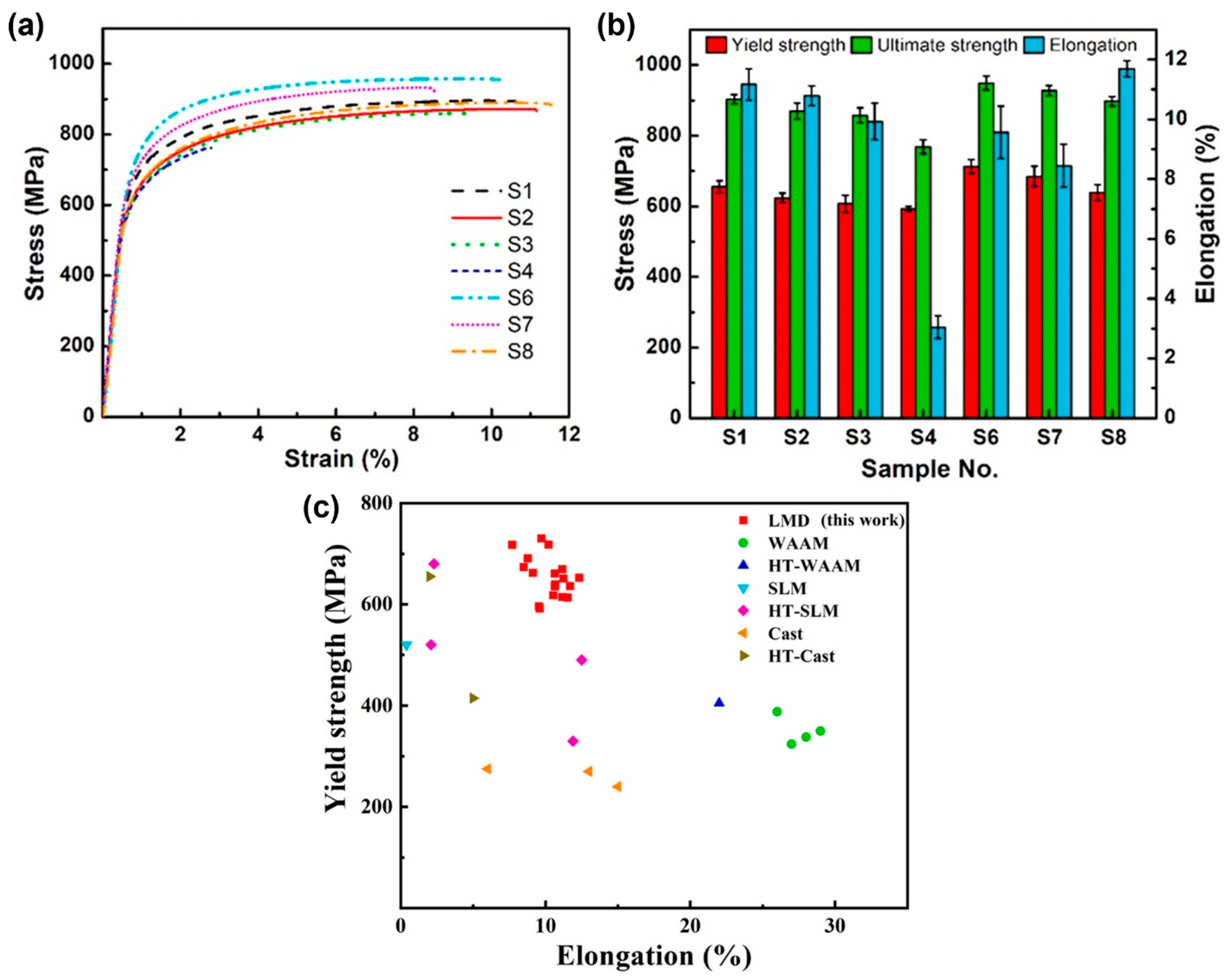
- In the case of the NAB alloys, the α-Cu matrix in cast parts contains four different intermetallic phases (κI, κII, κIII, and κIV), while WAAM produces a finer microstructure, eliminates κI, and reduces the content of other secondary phases due to the higher solidification rate. In contrast, beam-based AM processes, such as L-PBF, L-DED, and EBM, lead to the formation of a hard martensitic matrix due to even higher cooling rates. Overall, AM-fabricated NAB alloys exhibit higher mechanical properties than their cast counterparts due to the lower fraction and finer size of precipitates in WAAM parts and the formation of a martensitic matrix in beam-based AM processes. However, the columnar and heterogeneous microstructure of WAAM- and L-PBF-fabricated NABs results in anisotropic mechanical properties, while EBM-fabricated NABs contain a fairly homogeneous microstructure with a nearly equiaxed grain structure and near-isotropic tensile properties due to the relatively uniform heating cycles associated with EBM. Novel ultrasonic vibration-assisted WAAM systems or appropriate post-printing heat treatment cycles can minimize the columnar structure and anisotropic mechanical properties of AM-fabricated NABs.
Author Contributions
Funding
Acknowledgments
Conflicts of Interest
References
- Jiang, Q.; Zhang, P.; Yu, Z.; Shi, H.; Wu, D.; Yan, H.; Ye, X.; Lu, Q.; Tian, Y. A review on additive manufacturing of pure copper. Coatings 2021, 11, 740. [Google Scholar] [CrossRef]
- Tran, T.Q.; Chinnappan, A.; Lee, J.K.Y.; Loc, N.H.; Tran, L.T.; Wang, G.; Kumar, V.V.; Jayathilaka, W.; Ji, D.; Doddamani, M. 3D printing of highly pure copper. Metals 2019, 9, 756. [Google Scholar] [CrossRef]
- Malý, M.; Koutný, D.; Pantělejev, L.; Pambaguian, L.; Paloušek, D. Effect of high-temperature preheating on pure copper thick-walled samples processed by laser powder bed fusion. J. Manuf. Process. 2022, 73, 924–938. [Google Scholar] [CrossRef]
- Frigola, P.; Harrysson, O.; Horn, T.; West, H.; Aman, R.; Rigsbee, J.; Ramirez, D.; Medina, F.; Wicker, R.; Rodriguez, E. Fabricating copper components. Adv. Mater. Process. 2014, 172, 20–24. [Google Scholar]
- Guo, X.; Jia, L.; Lu, Z.; Xing, Z.; Xie, H.; Kondoh, K. Preparation of Cu/CrB2 composites with well-balanced mechanical properties and electrical conductivity by ex-situ powder metallurgy. J. Mater. Res. Technol. 2022, 17, 1605–1615. [Google Scholar] [CrossRef]
- Kohler, F.; Campanella, T.; Nakanishi, S.; Rappaz, M. Application of single pan thermal analysis to Cu–Sn peritectic alloys. Acta Mater. 2008, 56, 1519–1528. [Google Scholar] [CrossRef]
- Barik, R.C.; Wharton, J.A.; Wood, R.J.K.; Tan, K.S.; Stokes, K.R. Erosion and erosion–corrosion performance of cast and thermally sprayed nickel–aluminium bronze. Wear 2005, 259, 230–242. [Google Scholar] [CrossRef]
- Mao, Z.; Zhang, D.Z.; Jiang, J.; Fu, G.; Zhang, P. Processing optimisation, mechanical properties and microstructural evolution during selective laser melting of Cu-15Sn high-tin bronze. Mater. Sci. Eng. A 2018, 721, 125–134. [Google Scholar] [CrossRef]
- Walsh, F.C.; Low, C.T.J. A review of developments in the electrodeposition of tin-copper alloys. Surf. Coat. Technol. 2016, 304, 246–262. [Google Scholar] [CrossRef]
- Tavakoli, A.; Liu, R.; Wu, X.J. Improved mechanical and tribological properties of tin–bronze journal bearing materials with newly developed tribaloy alloy additive. Mater. Sci. Eng. A 2008, 489, 389–402. [Google Scholar] [CrossRef]
- Chiavari, C.; Colledan, A.; Frignani, A.; Brunoro, G. Corrosion evaluation of traditional and new bronzes for artistic castings. Mater. Chem. Phys. 2006, 95, 252–259. [Google Scholar] [CrossRef]
- Queguineur, A.; Rückert, G.; Cortial, F.; Hascoët, J.Y. Evaluation of wire arc additive manufacturing for large-sized components in naval applications. Weld. World. 2018, 62, 259–266. [Google Scholar] [CrossRef]
- Konečná, R.; Fintová, S. Copper and Copper Alloys: Casting, Classification and Characteristic Microstructures; InTech: Rijeka, Croatia, 2012. [Google Scholar]
- De Li, Z.; Lin, C.G.; Cui, S. Development of Research and Application of Copper Alloys with High Strength and High Conductivity; Advanced Materials Research; Trans Tech Publications, Ltd.: Wollerau, Switzerland, 2014; Volume 1053, pp. 61–68. [Google Scholar]
- Horn, T.J.; Gamzina, D. Additive manufacturing of copper and copper alloys. In ASM Handbook; ASM International: Novelty, OH, USA, 2020. [Google Scholar]
- Müller, R. Arc-melted CuCr alloys as contact materials for vacuum interrupters. Siemens Forsch.-Und Entwicklungsberichte 1988, 17, 105–111. [Google Scholar]
- Ghosh, S.K.; Grover, A.K.; Dey, G.K.; Totlani, M.K. Nanocrystalline Ni–Cu alloy plating by pulse electrolysis. Surf. Coat. Technol. 2000, 126, 48–63. [Google Scholar] [CrossRef]
- Sequeira, C.A.C.; Cardoso, D.S.P.; Amaral, L.; Šljukić, B.; Santos, D.M.F. On the performance of commercially available corrosion-resistant nickel alloys: A review. Corros. Rev. 2016, 34, 187–200. [Google Scholar] [CrossRef]
- Orzolek, S.M.; Semple, J.K.; Fisher, C.R. Influence of Processing on the Microstructure of Nickel Aluminum Bronze (NAB). Addit. Manuf. 2022, 56, 102859. [Google Scholar] [CrossRef]
- Richardson, I. Guide to Nickel Aluminium Bronze for Engineers; Copper Development Association: McLean, VA, USA, 2016. [Google Scholar]
- Weston, G.M. Survey of Nickel-Aluminium-Bronze Casting Alloys on Marine Applications; Materials Research Labs: Ascot Vale, Australia, 1981. [Google Scholar]
- Kim, J.; Kim, J.; Pyo, C. Comparison of Mechanical Properties of Ni-Al-Bronze Alloy Fabricated through Wire Arc Additive Manufacturing with Ni-Al-Bronze Alloy Fabricated through Casting. Metals 2020, 10, 1164. [Google Scholar] [CrossRef]
- Corona, D.; Beatrici, M.; Sbardella, E.; Di Domenico, G.; Lucibello, F.; Zarcone, M.; Del Gaudio, C. 3D printing copper—Graphene oxide nanocomposites. AIP Conf. Proc. 2021, 2416, 20007. [Google Scholar] [CrossRef]
- Dadkhah, M.; Saboori, A.; Fino, P. An Overview of the Recent Developments in Metal Matrix Nanocomposites Reinforced by Graphene. Materials 2019, 12, 2823. [Google Scholar] [CrossRef] [PubMed]
- Han, T.; Li, J.; Zhao, N.; Shi, C.; Liu, E.; He, F.; Ma, L.; Li, Q.; He, C. In-situ fabrication of nano-sized TiO2 reinforced Cu matrix composites with well-balanced mechanical properties and electrical conductivity. Powder Technol. 2017, 321, 66–73. [Google Scholar] [CrossRef]
- Campagnoli, M.R.; Galati, M.; Saboori, A. On the processability of copper components via powder-based additive manufacturing processes: Potentials, challenges and feasible solutions. J. Manuf. Process. 2021, 72, 320–337. [Google Scholar] [CrossRef]
- Constantin, L.; Wu, Z.; Li, N.; Fan, L.; Silvain, J.-F.; Lu, Y.F. Laser 3D printing of complex copper structures. Addit. Manuf. 2020, 35, 101268. [Google Scholar] [CrossRef]
- JPark, S.; Park, C.W.; Lee, K.J. Implication of peritectic composition in historical high-tin bronze metallurgy. Mater. Charact. 2009, 60, 1268–1275. [Google Scholar] [CrossRef]
- Souissi, N.; Sidot, E.; Bousselmi, L.; Triki, E.; Robbiola, L. Corrosion behaviour of Cu–10Sn bronze in aerated NaCl aqueous media—Electrochemical investigation. Corros. Sci. 2007, 49, 3333–3347. [Google Scholar] [CrossRef]
- Zhang, C.; Yang, Z.; Wang, Y.; Ding, B.; Guo, Y. Preparation of CuCr25 contact materials by vacuum induction melting. J. Mater. Process. Technol. 2006, 178, 283–286. [Google Scholar] [CrossRef]
- Zhao, L.; Li, Z.; Shi, K.; He, J.; Li, H. Electrical properties of nanocrystalline CuCr25 contact material. IEEE Trans. Compon. Packag. Manuf. Technol. 2012, 3, 625–632. [Google Scholar] [CrossRef]
- Wang, Y.; Ding, B. The preparation and the properties of microcrystalline and nanocrystalline CuCr contact materials. IEEE Trans. Compon. Packag. Technol. 1999, 22, 467–472. [Google Scholar] [CrossRef]
- Yadav, S.; Jinoop, A.N.; Sinha, N.; Paul, C.P.; Bindra, K.S. Parametric investigation and characterization of laser directed energy deposited copper-nickel graded layers. Int. J. Adv. Manuf. Technol. 2020, 108, 3779–3791. [Google Scholar] [CrossRef]
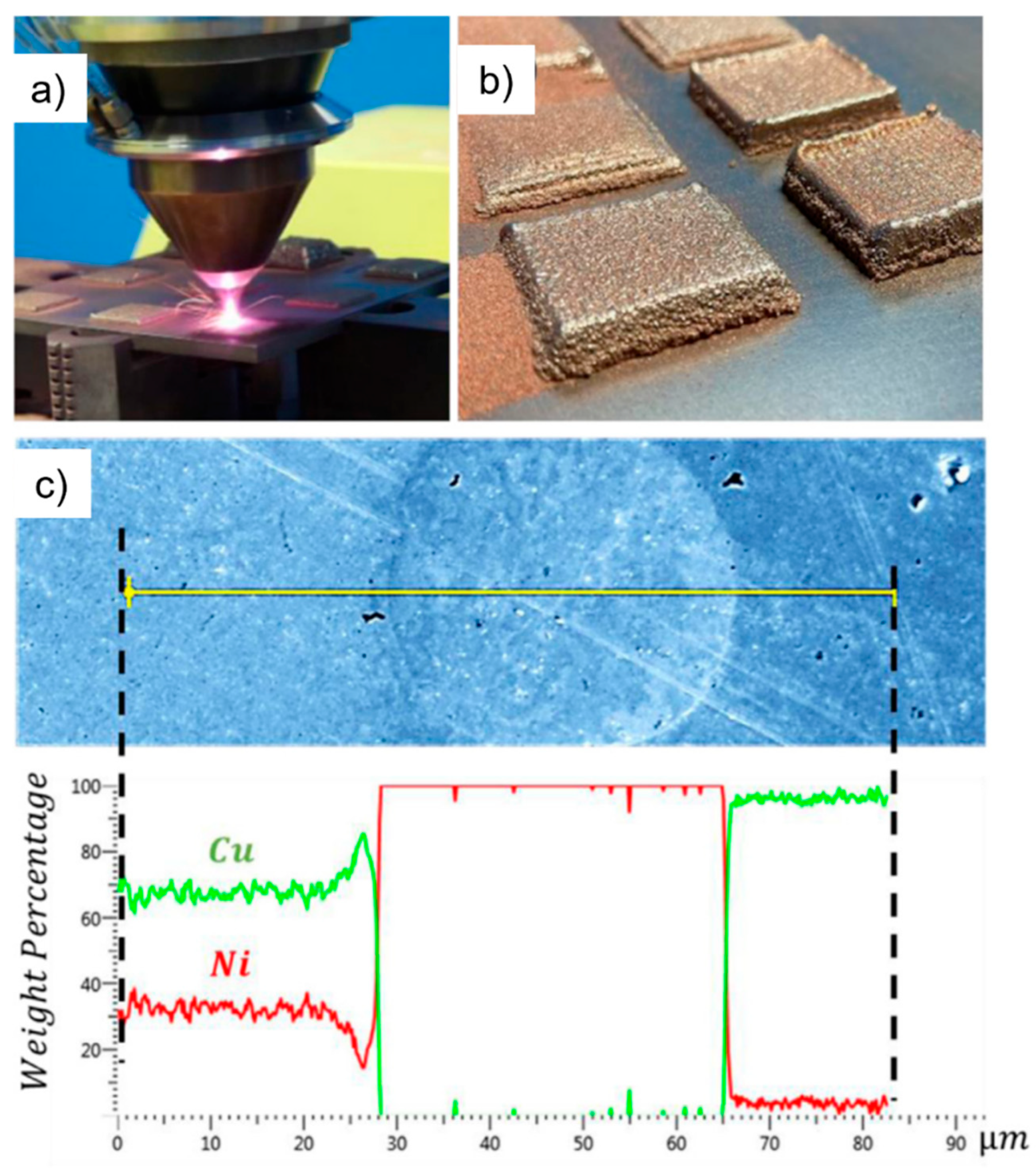
- Zhang, X.; Li, L.; Pan, T.; Chen, Y.; Zhang, Y.; Li, W.; Liou, F. Additive manufacturing of copper-tool steel dissimilar joining: Experimental characterization and thermal modeling. Mater. Charact. 2020, 170, 110692. [Google Scholar] [CrossRef]
- Zhang, X.; Pan, T.; Chen, Y.; Li, L.; Zhang, Y.; Liou, F. Additive manufacturing of copper-stainless steel hybrid components using laser-aided directed energy deposition. J. Mater. Sci. Technol. 2021, 80, 100–116. [Google Scholar] [CrossRef]
- Zhang, X.; Pan, T.; Flood, A.; Chen, Y.; Zhang, Y.; Liou, F. Investigation of copper/stainless steel multi-metallic materials fabricated by laser metal deposition. Mater. Sci. Eng. A 2021, 811, 141071. [Google Scholar] [CrossRef]
- Prasad, H.S.; Brueckner, F.; Volpp, J.; Kaplan, A.F.H. Laser metal deposition of copper on diverse metals using green laser sources. Int. J. Adv. Manuf. Technol. 2020, 107, 1559–1568. [Google Scholar] [CrossRef]
- Al-Fozan, S.A.; Malik, A.U. MSF evaporator materials evaluation after 20 years in service. Desalin. Water Treat. 2009, 2, 345–352. [Google Scholar] [CrossRef]
- Bandyopadhyay, A.; Heer, B. Additive manufacturing of multi-material structures. Mater. Sci. Eng. R Rep. 2018, 129, 1–16. [Google Scholar] [CrossRef]
- Xia, C.; Pan, Z.; Polden, J.; Li, H.; Xu, Y.; Chen, S.; Zhang, Y. A review on wire arc additive manufacturing: Monitoring, control and a framework of automated system. J. Manuf. Syst. 2020, 57, 31–45. [Google Scholar] [CrossRef]
- Ge, J.; Lin, J.; Lei, Y.; Fu, H. Location-related thermal history, microstructure, and mechanical properties of arc additively manufactured 2Cr13 steel using cold metal transfer welding. Mater. Sci. Eng. A 2018, 715, 144–153. [Google Scholar] [CrossRef]
- Gibson, I.; Rosen, D.W.; Stucker, B.; Khorasani, M. Additive Manufacturing Technologies; Springer: Berlin/Heidelberg, Germany, 2021. [Google Scholar]
- Sun, Y.; Hebert, R.J.; Aindow, M. Effect of heat treatments on microstructural evolution of additively manufactured and wrought 17-4PH stainless steel. Mater. Des. 2018, 156, 429–440. [Google Scholar] [CrossRef]
- Liberini, M.; Astarita, A.; Campatelli, G.; Scippa, A.; Montevecchi, F.; Venturini, G.; Durante, M.; Boccarusso, L.; Minutolo, F.M.C.; Squillace, A. Selection of Optimal Process Parameters for Wire Arc Additive Manufacturing. Procedia Cirp 2017, 62, 470–474. [Google Scholar] [CrossRef]
- Thijs, L.; Sistiaga, M.L.M.; Wauthle, R.; Xie, Q.; Kruth, J.-P.; Van Humbeeck, J. Strong morphological and crystallographic texture and resulting yield strength anisotropy in selective laser melted tantalum. Acta Mater. 2013, 61, 4657–4668. [Google Scholar] [CrossRef]
- Carter, L.N.; Martin, C.; Withers, P.J.; Attallah, M.M. The influence of the laser scan strategy on grain structure and cracking behaviour in SLM powder-bed fabricated nickel superalloy. J. Alloys Compd. 2014, 615, 338–347. [Google Scholar] [CrossRef]
- Carroll, B.E.; Palmer, T.A.; Beese, A.M. Anisotropic tensile behavior of Ti-6Al-4V components fabricated with directed energy deposition additive manufacturing. Acta Mater. 2015, 87, 309–320. [Google Scholar] [CrossRef]
- Zhang, Q.; Chen, J.; Zhao, Z.; Tan, H.; Lin, X.; Huang, W. Microstructure and anisotropic tensile behavior of laser additive manufactured TC21 titanium alloy. Mater. Sci. Eng. A 2016, 673, 204–212. [Google Scholar] [CrossRef]
- Ikeshoji, T.-T.; Nakamura, K.; Yonehara, M.; Imai, K.; Kyogoku, H. Selective laser melting of pure copper. JOM 2018, 70, 396–400. [Google Scholar] [CrossRef]
- Lykov, P.A.; Safonov, E.V.; Akhmedianov, A.M. Selective Laser Melting of Copper; Materials Science Forum; Trans Tech Publications Ltd.: Stafa, Switzerland, 2016; Volume 843, pp. 284–288. [Google Scholar] [CrossRef]
- El-Wardany, T.I.; She, Y.; Jagdale, V.N.; Garofano, J.K.; Liou, J.J.; Schmidt, W.R. Challenges in three-dimensional printing of high-conductivity copper. J. Electron. Packag. 2018, 140, 20907. [Google Scholar] [CrossRef]
- Guan, J.; Zhang, X.; Jiang, Y.; Yan, Y. Insights into fabrication mechanism of pure copper thin wall components by selective infrared laser melting. Rapid Prototyp. J. 2019, 25, 1388–1397. [Google Scholar] [CrossRef]
- Pogson, S.R.; Fox, P.; Sutcliffe, C.J.; O’neill, W. The production of copper parts using DMLR. Rapid Prototyp. J. 2003, 9, 334–343. [Google Scholar] [CrossRef]
- Silbernagel, C.; Gargalis, L.; Ashcroft, I.; Hague, R.; Galea, M.; Dickens, P. Electrical resistivity of pure copper processed by medium-powered laser powder bed fusion additive manufacturing for use in electromagnetic applications. Addit. Manuf. 2019, 29, 100831. [Google Scholar] [CrossRef]
- Colopi, M.; Demir, A.G.; Caprio, L.; Previtali, B. Limits and solutions in processing pure Cu via selective laser melting using a high-power single-mode fiber laser. Int. J. Adv. Manuf. Technol. 2019, 104, 2473–2486. [Google Scholar] [CrossRef]
- Jadhav, S.D.; Dadbakhsh, S.; Goossens, L.; Kruth, J.-P.; Van Humbeeck, J.; Vanmeensel, K. Influence of selective laser melting process parameters on texture evolution in pure copper. J. Mater. Process. Technol. 2019, 270, 47–58. [Google Scholar] [CrossRef]
- Gruber, S.; Stepien, L.; López, E.; Brueckner, F.; Leyens, C. Physical and geometrical properties of additively manufactured pure copper samples using a green laser source. Materials 2021, 14, 3642. [Google Scholar] [CrossRef]
- Hori, E.; Sato, Y.; Shibata, T.; Tojo, K.; Tsukamoto, M. Development of SLM process using 200 W blue diode laser for pure copper additive manufacturing of high density structure. J. Laser Appl. 2021, 33, 12008. [Google Scholar] [CrossRef]
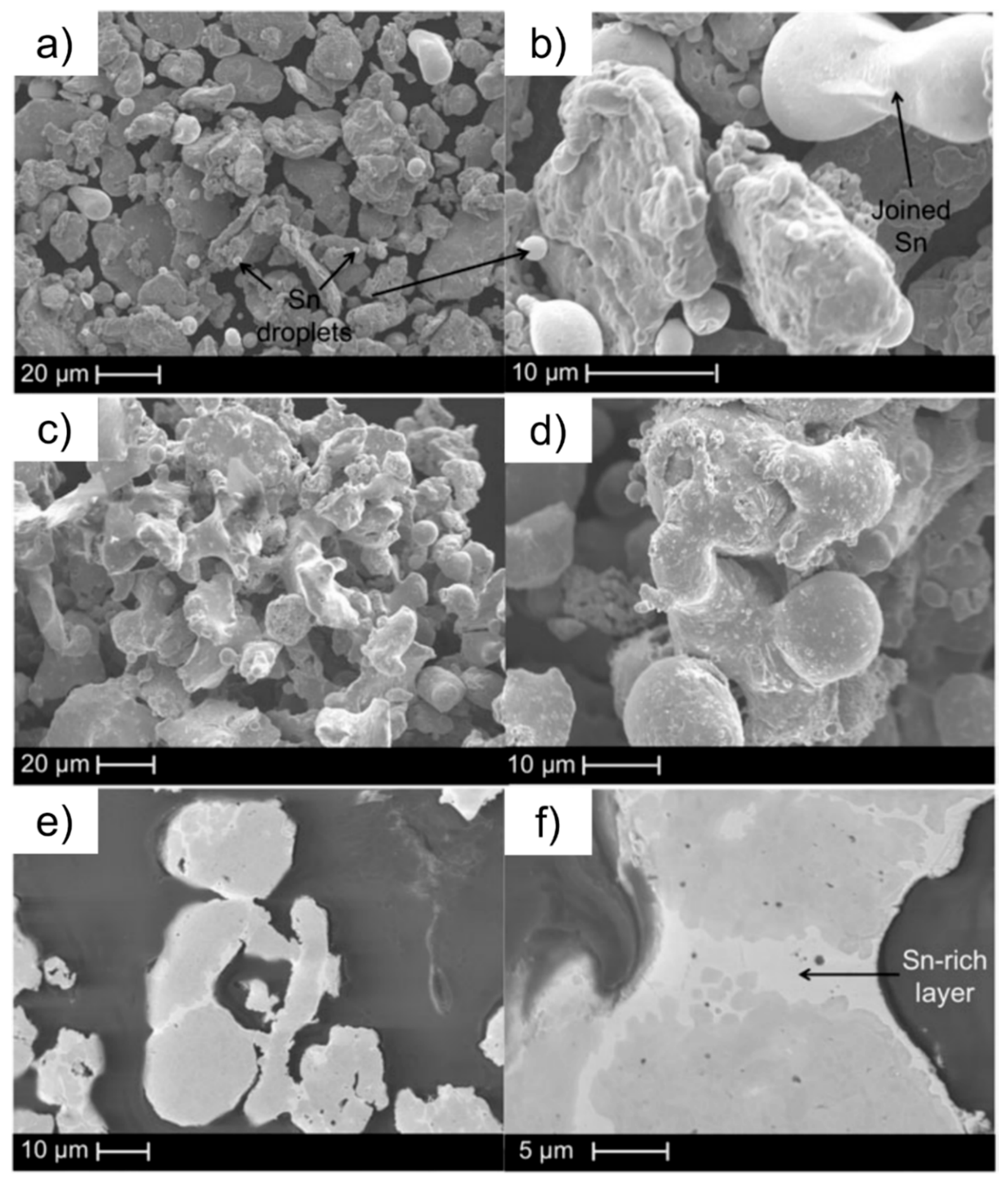
- Jadhav, S.D.; Fu, D.; Deprez, M.; Ramharter, K.; Willems, D.; Van Hooreweder, B.; Vanmeensel, K. Highly conductive and strong CuSn0. 3 alloy processed via laser powder bed fusion starting from a tin-coated copper powder. Addit. Manuf. 2020, 36, 101607. [Google Scholar]
- Zhang, S.; Zhu, H.; Zhang, L.; Zhang, W.; Yang, H.; Zeng, X. Microstructure and properties of high strength and high conductivity Cu-Cr alloy components fabricated by high power selective laser melting. Mater. Lett. 2019, 237, 306–309. [Google Scholar] [CrossRef]
- Zhang, S.; Zhu, H.; Zhang, L.; Zhang, W.; Yang, H.; Zeng, X. Microstructure and properties in QCr0. 8 alloy produced by selective laser melting with different heat treatment. J. Alloys Compd. 2019, 800, 286–293. [Google Scholar] [CrossRef]
- Uchida, S.; Kimura, T.; Nakamoto, T.; Ozaki, T.; Miki, T.; Takemura, M.; Oka, Y.; Tsubota, R. Microstructures and electrical and mechanical properties of Cu-Cr alloys fabricated by selective laser melting. Mater. Des. 2019, 175, 107815. [Google Scholar] [CrossRef]
- Jadhav, S.D.; Dadbakhsh, S.; Chen, R.; Shabadi, R.; Kruth, J.-P.; Van Humbeeck, J.; Vanmeensel, K. Modification of Electrical and Mechanical Properties of Selective Laser-Melted CuCr0.3 Alloy Using Carbon Nanoparticles. Adv. Eng. Mater. 2020, 22, 1900946. [Google Scholar] [CrossRef]
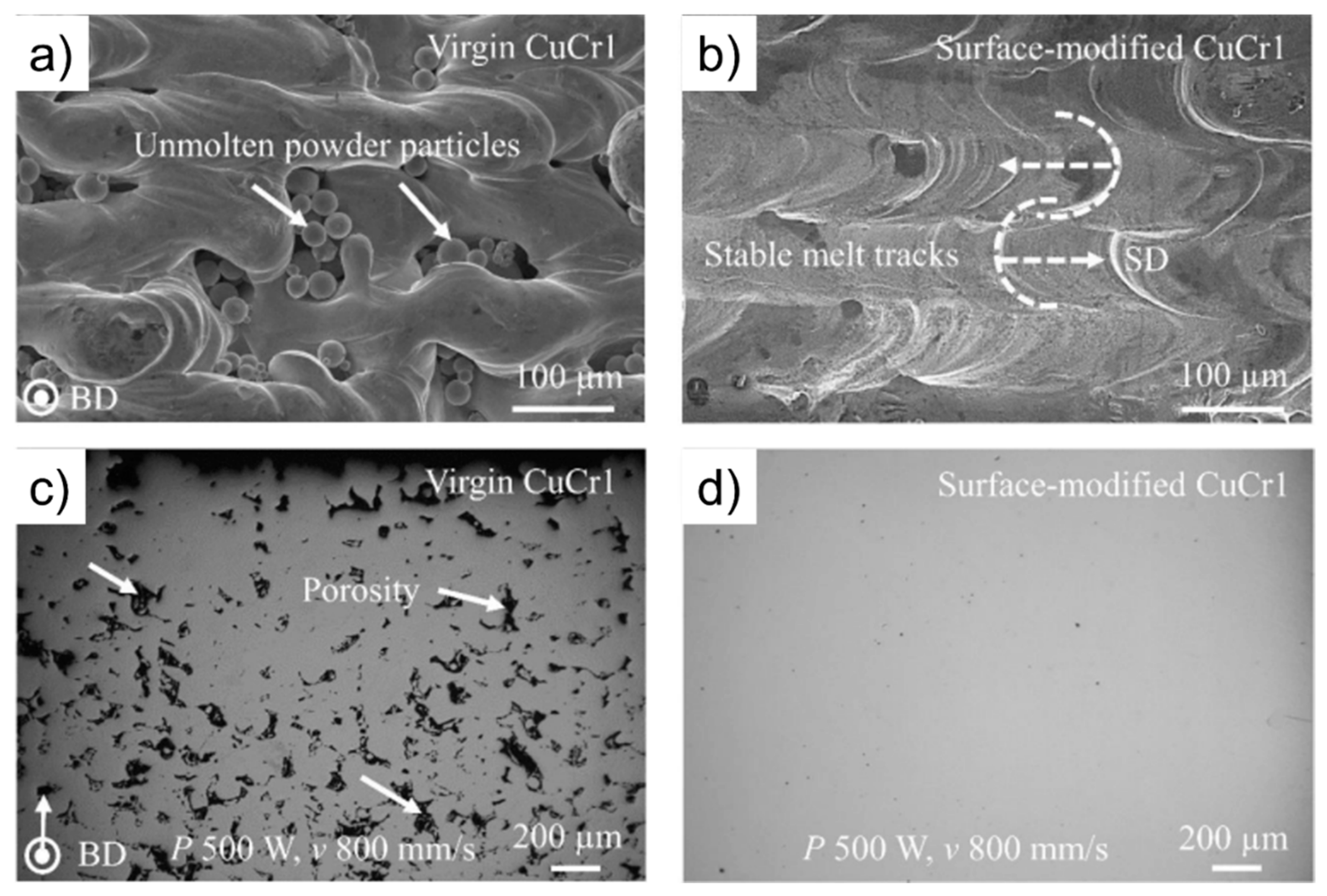
- Jadhav, S.D.; Dhekne, P.P.; Dadbakhsh, S.; Kruth, J.-P.; Van Humbeeck, J.; Vanmeensel, K. Surface modified copper alloy powder for reliable laser-based additive manufacturing. Addit. Manuf. 2020, 35, 101418. [Google Scholar] [CrossRef]
- Jadhav, S.D.; Dhekne, P.P.; Brodu, E.; Van Hooreweder, B.; Dadbakhsh, S.; Kruth, J.-P.; Van Humbeeck, J.; Vanmeensel, K. Laser powder bed fusion additive manufacturing of highly conductive parts made of optically absorptive carburized CuCr1 powder. Mater. Des. 2021, 198, 109369. [Google Scholar] [CrossRef]
- Shen, J.; Li, Z.; Li, H.; Yao, B.; Teng, B. Additive manufacturing of high relative density Cu-0.8 Cr alloy by low power 1064 nm Yb-fiber laser powder bed fusion: Role of Nano-TiC modification. Mater. Lett. 2022, 308, 131141. [Google Scholar] [CrossRef]
- Chen, Y.; Ren, S.; Zhao, Y.; Qu, X. Microstructure and properties of CuCr alloy manufactured by selective laser melting. J. Alloys Compd. 2019, 786, 189–197. [Google Scholar] [CrossRef]
- Dou, Z.H.; Zhang, T.A.; Hao, J.C. Research progress of Cu-Cr alloy contact materials. Mater. Rev. 2005, 19, 63–68. [Google Scholar]
- Wu, X.; Zhou, X.; Cui, H.; Zheng, X.; Zhang, J. Deposition behavior and characteristics of cold-sprayed Cu-Cr composite deposits. J. Therm. Spray Technol. 2012, 21, 792–799. [Google Scholar] [CrossRef]
- Rieder, W.F.; Schussek, M.; Glatzle, W.; Kny, E. The influence of composition and Cr particle size of Cu/Cr contacts on chopping current, contact resistance, and breakdown voltage in vacuum interrupters. IEEE Trans. Compon. Hybrids Manuf. Technol. 1989, 12, 273–283. [Google Scholar] [CrossRef]
- Shangina, D.V.; Gubicza, J.; Dodony, E.; Bochvar, N.R.; Straumal, P.B.; Tabachkova, N.Y.; Dobatkin, S.V. Improvement of strength and conductivity in Cu-alloys with the application of high pressure torsion and subsequent heat-treatments. J. Mater. Sci. 2014, 49, 6674–6681. [Google Scholar] [CrossRef]
- Jin, Y.; Adachi, K.; Takeuchi, T.; Suzuki, H.G. Correlation between the electrical conductivity and aging treatment for a Cu-15 wt% Cr alloy composite formed in-situ. Mater. Lett. 1997, 32, 307–311. [Google Scholar] [CrossRef]
- Zhang, S.; Li, R.; Kang, H.; Chen, Z.; Wang, W.; Zou, C.; Li, T.; Wang, T. A high strength and high electrical conductivity Cu-Cr-Zr alloy fabricated by cryorolling and intermediate aging treatment. Mater. Sci. Eng. A 2017, 680, 108–114. [Google Scholar] [CrossRef]
- Jia, S.G.; Zheng, M.S.; Liu, P.; Ren, F.Z.; Tian, B.H.; Zhou, G.S.; Lou, H.F. Aging properties studies in a Cu–Ag–Cr alloy. Mater. Sci. Eng. A 2006, 419, 8–11. [Google Scholar] [CrossRef]
- Harzer, T.P.; Duarte, M.J.; Dehm, G. In–situ TEM study of diffusion kinetics and electron irradiation effects on the Cr phase separation of a nanocrystalline Cu–4 at.% Cr thin film alloy. J. Alloys Compd. 2017, 695, 1583–1590. [Google Scholar] [CrossRef]
- Liu, P.; Kang, B.X.; Cao, X.G.; Huang, J.L.; Gu, H.C. Strengthening mechanisms in a rapidly solidified and aged Cu-Cr alloy. J. Mater. Sci. 2000, 35, 1691–1694. [Google Scholar] [CrossRef]
- Doi, T. Studies on copper alloys containing chromium on the copper side phase diagram. Nippon. Kinzoku Gakkaishi 1957, 21, 337–340. [Google Scholar]
- Nishikawa, S.; Nagata, K.; Kobayashi, S. The aging process of Cu-Cr alloys. JAP Inst. Metals J. 1966, 30, 302–307. [Google Scholar] [CrossRef]
- Zhang, X.G. Galvanic corrosion. In Uhlig’s Corrosion Handbook; John Wiley & Sons: Hoboken, NJ, USA, 2011; Volume 51, p. 123. [Google Scholar]
- Yu, R.; Zhu, Z.; Li, B.; Lu, Y.; Fu, B.; Guan, R.; Lu, X. Performance improvement of laser additive manufactured Cu–Cr alloy via continuous extrusion. J. Alloys Compd. 2021, 879, 160475. [Google Scholar] [CrossRef]
- Xiu, S.; Ren, Y.; Jun, X.; Wang, J.; Wang, J. Microstructure and properties of CuCr contact materials with different Cr content. Trans. Nonferrous Met. Soc. China 2011, 21, s389–s393. [Google Scholar] [CrossRef]
- Maeda, K.; Niitsu, A.; Morito, H.; Shiga, K.; Fujiwara, K. In situ observation of grain boundary groove at the crystal/melt interface in Cu. Scr. Mater. 2018, 146, 169–172. [Google Scholar] [CrossRef]
- Lu, L.; Chen, X.; Huang, X.; Lu, K. Revealing the maximum strength in nanotwinned copper. Science 2009, 323, 607–610. [Google Scholar] [CrossRef] [PubMed]
- Momeni, S.; Guschlbauer, R.; Osmanlic, F.; Körner, C. Selective electron beam melting of a copper-chrome powder mixture. Mater. Lett. 2018, 223, 250–252. [Google Scholar] [CrossRef]
- Guo, C.; Kang, T.; Wu, S.; Ying, M.; Liu, W.M.; Chen, F. Microstructure, mechanical, and corrosion resistance of copper nickel alloy fabricated by wire-arc additive manufacturing. MRS Commun. 2021, 11, 910–916. [Google Scholar] [CrossRef]
- Rajesh, R.; Kulkarni, M.V.; Vergis, B.R.; Sampathkumaran, P.; Seetharamu, S. Copper nickel alloys made using direct metal laser sintering method for assessing corrosion resistance properties. Mater. Today Proc. 2022, 49, 703–713. [Google Scholar] [CrossRef]
- Vinod, A.R.; Srinivasa, C.K. Studies on laser-sintering of copper by direct metal laser sintering process. In Proceedings of the 5th International and 26th All India Manufacturing Technology, Design and Research Conference AIMTDR 2014, Kolkata, India, 12–14 December 2014; pp. 371–377. [Google Scholar]
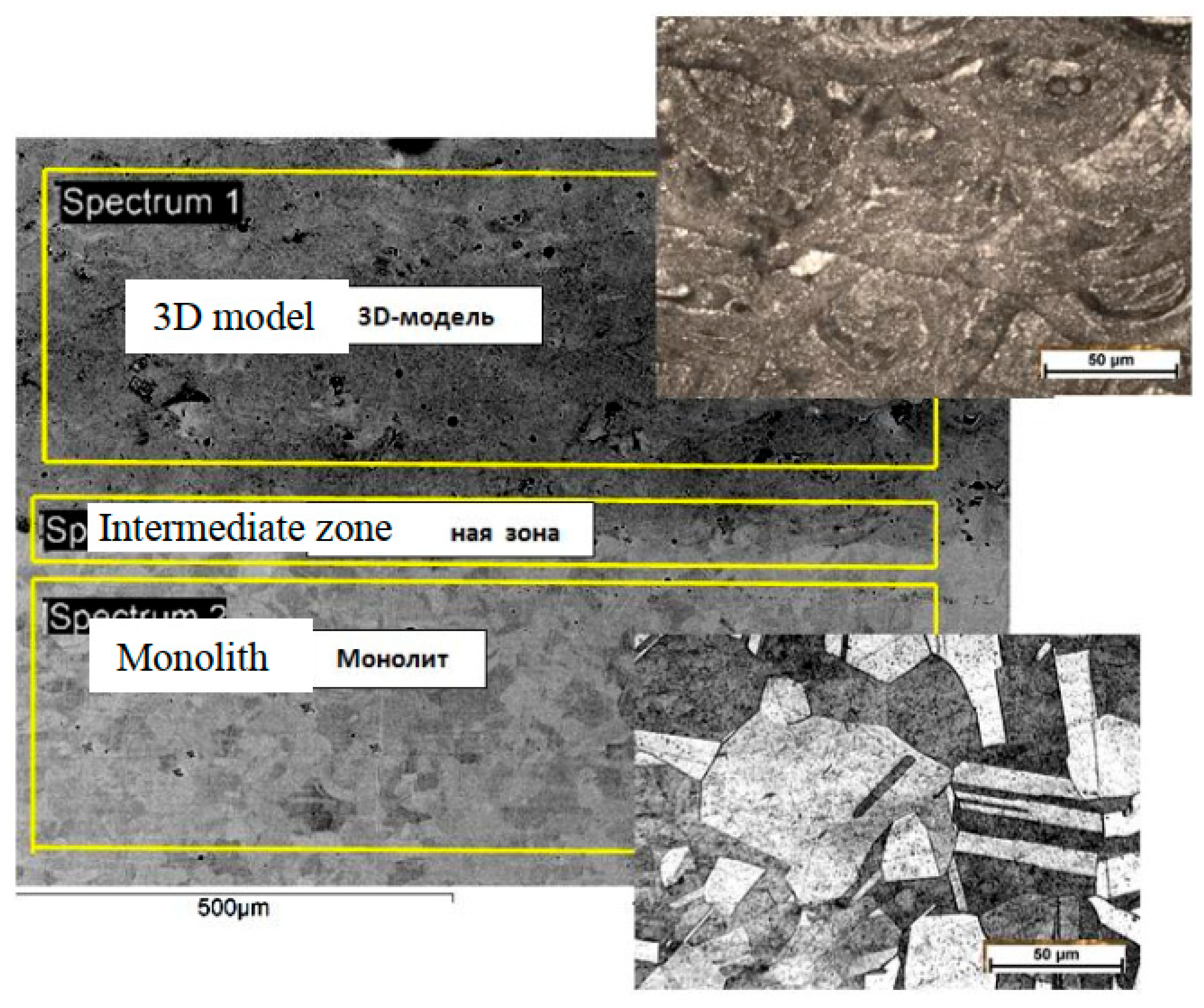
- Baraz, V.R.; Gerasimov, S.S.; Gruzdeva, I.A.; Shveikin, V.P.; Chemesova, A.V.; Ovchinnikova, A.O.; Veretennikova, I.A. The additive technology to obtain a three-dimensional model of the 81Cu-19Ni alloy. IOP Conf. Ser. Mater. Sci. Eng. 2020, 966, 12119. [Google Scholar] [CrossRef]
- Sabelle, M.; Walczak, M.; Ramos-Grez, J. Scanning pattern angle effect on the resulting properties of selective laser sintered monolayers of Cu-Sn-Ni powder. Opt. Lasers Eng. 2018, 100, 1–8. [Google Scholar] [CrossRef]
- Leong, C.C.; Lu, L.; Fuh, J.Y.H.; Wong, Y.S. In-situ formation of copper matrix composites by laser sintering. Mater. Sci. Eng. A 2002, 338, 81–88. [Google Scholar] [CrossRef]
- Katiyar, A.; Gupta, A.; Verma, J.; Yadav, A. Effect of water parameters on corrosion behaviour of mild steel in immersed and atmospheric conditions. Int. Res. J. Mod. Eng. Technol. Sci. 2020, 2, 1641–1650. [Google Scholar]
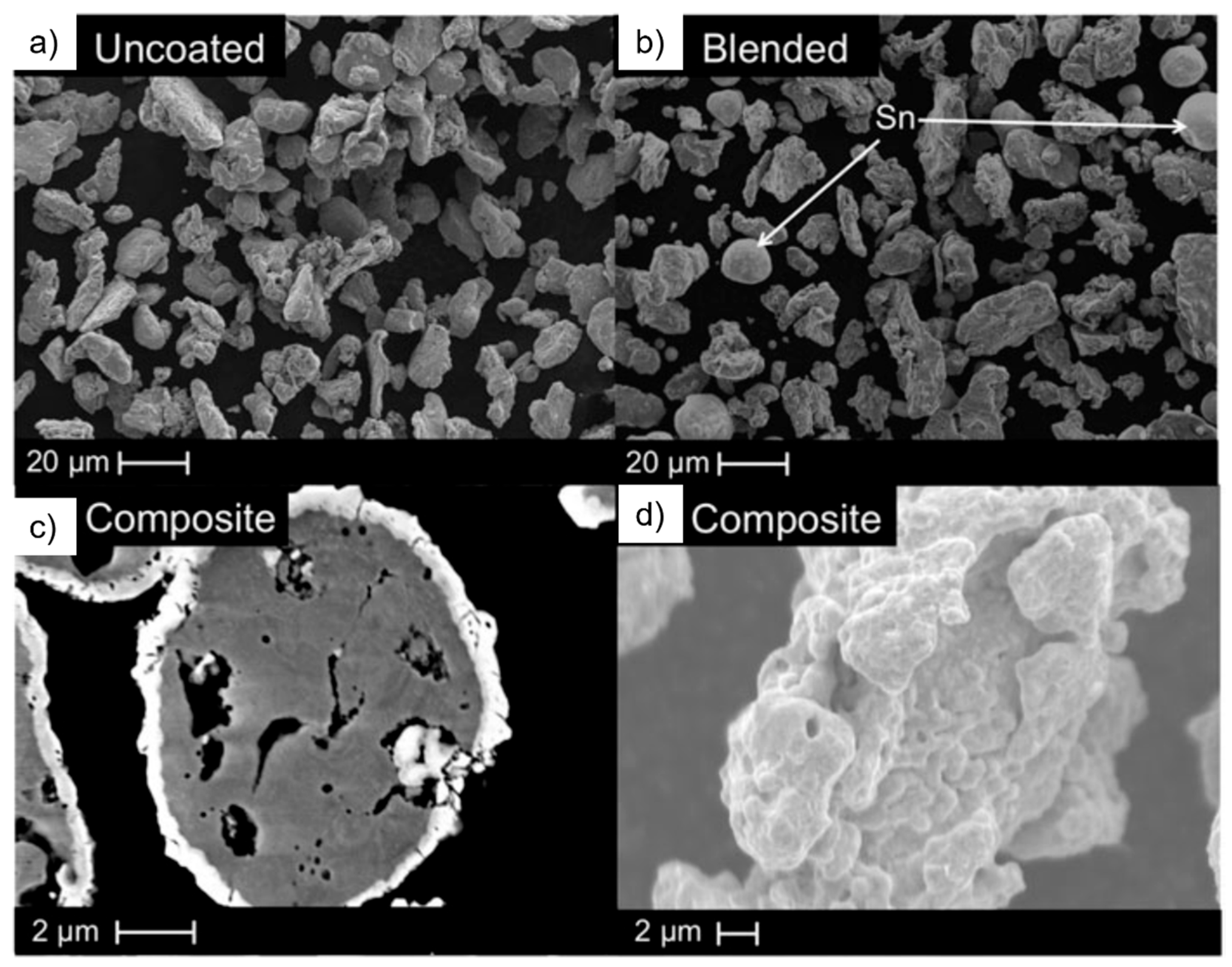
- Karnati, S.; Liou, F.F.; Newkirk, J.W. Characterization of copper–nickel alloys fabricated using laser metal deposition and blended powder feedstocks. Int. J. Adv. Manuf. Technol. 2019, 103, 239–250. [Google Scholar] [CrossRef]
- Karnati, S.; Zhang, Y.; Liou, F.F.; Newkirk, J.W. On the feasibility of tailoring copper–nickel functionally graded materials fabricated through laser metal deposition. Metals 2019, 9, 287. [Google Scholar] [CrossRef]
- Li, S.; Snyder, K.; Akhanda, M.S.; Martukanitz, R.; Mitra, M.; Poon, J.; Zebarjadi, M. Cost-efficient copper-nickel alloy for active cooling applications. Int. J. Heat Mass Transf. 2022, 195, 123181. [Google Scholar] [CrossRef]
- Pugachevich, P.P.; Yashkichev, V.I. Temperature-dependence of the surface tension of copper. Bull. Acad. Sci. USSR Div. Chem. Sci. 1959, 8, 782–786. [Google Scholar] [CrossRef]
- Haley, J.C.; Schoenung, J.M.; Lavernia, E.J. Modelling particle impact on the melt pool and wettability effects in laser directed energy deposition additive manufacturing. Mater. Sci. Eng. A 2019, 761, 138052. [Google Scholar] [CrossRef]
- Jinoop, A.N.; Denny, J.; Paul, C.P.; Kumar, J.G.; Bindra, K.S. Effect of post heat-treatment on the microstructure and mechanical properties of Hastelloy-X structures manufactured by laser based Directed Energy Deposition. J. Alloys Compd. 2019, 797, 399–412. [Google Scholar] [CrossRef]
- Hasegawa, M. Ellingham diagram. In Treatise Process Metall; Elsevier: Amsterdam, The Netherlands, 2014; pp. 507–516. [Google Scholar]
- Leung, C.L.A.; Marussi, S.; Towrie, M.; Atwood, R.C.; Withers, P.J.; Lee, P.D. The effect of powder oxidation on defect formation in laser additive manufacturing. Acta Mater. 2019, 166, 294–305. [Google Scholar] [CrossRef]
- Diabb, J.; Juárez-Hernandez, A.; Colas, R.; Castillo, A.G.; García-Sanchez, E.; Hernandez-Rodriguez, M.A.L. Boron influence on wear resistance in nickel-based alloys. Wear 2009, 267, 550–555. [Google Scholar] [CrossRef]
- Lu, J.; Lu, H.; Xu, X.; Yao, J.; Cai, J.; Luo, K. High-performance integrated additive manufacturing with laser shock peening–induced microstructural evolution and improvement in mechanical properties of Ti6Al4V alloy components. Int. J. Mach. Tools Manuf. 2020, 148, 103475. [Google Scholar] [CrossRef]
- Rupert, T.J. Solid solution strengthening and softening due to collective nanocrystalline deformation physics. Scr. Mater. 2014, 81, 44–47. [Google Scholar] [CrossRef]
- Davis, J.R. Copper and Copper Alloys; ASM International: Novelty, OH, USA, 2001. [Google Scholar]
- Scudino, S.; Unterdörfer, C.; Prashanth, K.G.; Attar, H.; Ellendt, N.; Uhlenwinkel, V.; Eckert, J. Additive manufacturing of Cu–10Sn bronze. Mater. Lett. 2015, 156, 202–204. [Google Scholar] [CrossRef]
- Zheng, B.; Zhou, Y.; Smugeresky, J.E.; Lavernia, E.J. Processing and Behavior of Fe-Based Metallic Glass Components via Laser-Engineered Net Shaping. Metall. Mater. Trans. A 2009, 40, 1235–1245. [Google Scholar] [CrossRef]
- Inoue, A. Stabilization of metallic supercooled liquid and bulk amorphous alloys. Acta Mater. 2000, 48, 279–306. [Google Scholar] [CrossRef]
- Chen, X.; Wang, Z.; Ding, D.; Tang, H.; Qiu, L.; Luo, X.; Shi, G. Strengthening and toughening strategies for tin bronze alloy through fabricating in-situ nanostructured grains. Mater. Des. 2015, 66, 60–66. [Google Scholar] [CrossRef]
- Prashanth, K.G.; Scudino, S.; Klauss, H.J.; Surreddi, K.B.; Löber, L.; Wang, Z.; Chaubey, A.K.; Kühn, U.; Eckert, J. Microstructure and mechanical properties of Al–12Si produced by selective laser melting: Effect of heat treatment. Mater. Sci. Eng. A 2014, 590, 153–160. [Google Scholar] [CrossRef]
- Scudino, S.; Liu, G.; Sakaliyska, M.; Surreddi, K.B.; Eckert, J. Powder metallurgy of Al-based metal matrix composites reinforced with β-Al3Mg2 intermetallic particles: Analysis and modeling of mechanical properties. Acta Mater. 2009, 57, 4529–4538. [Google Scholar] [CrossRef]
- Karthik, G.M.; Sathiyamoorthi, P.; Zargaran, A.; Park, J.M.; Asghari-Rad, P.; Son, S.; Park, S.H.; Kim, H.S. Novel precipitation and enhanced tensile properties in selective laser melted Cu-Sn alloy. Materialia 2020, 13, 100861. [Google Scholar] [CrossRef]
- Kini, A.R.; Maischner, D.; Weisheit, A.; Ponge, D.; Gault, B.; Jägle, E.A.; Raabe, D. In-situ synthesis via laser metal deposition of a lean Cu–3.4 Cr–0.6 Nb (at%) conductive alloy hardened by Cr nano-scale precipitates and by Laves phase micro-particles. Acta Mater. 2020, 197, 330–340. [Google Scholar] [CrossRef]
- Chbihi, A.; Sauvage, X.; Blavette, D. Atomic scale investigation of Cr precipitation in copper. Acta Mater. 2012, 60, 4575–4585. [Google Scholar] [CrossRef]
- Hamana, D.; Boumerzoug, Z.; Fatmi, M.; Chekroud, S. Discontinuous and continuous precipitation in Cu-13 wt.% Sn and Al-20 wt.% Ag alloys. Mater. Chem. Phys. 1998, 53, 208–216. [Google Scholar] [CrossRef]
- Hooper, P.A. Melt pool temperature and cooling rates in laser powder bed fusion. Addit. Manuf. 2018, 22, 548–559. [Google Scholar] [CrossRef]
- Deng, C.; Kang, J.; Feng, T.; Feng, Y.; Wang, X.; Wu, P. Study on the selective laser melting of CuSn10 powder. Materials 2018, 11, 614. [Google Scholar] [CrossRef] [PubMed]
- Simchi, A.; Petzoldt, F.; Pohl, H. On the development of direct metal laser sintering for rapid tooling. J. Mater. Process. Technol. 2003, 141, 319–328. [Google Scholar] [CrossRef]
- Zhang, G.; Chen, C.; Wang, X.; Wang, P.; Zhang, X.; Gan, X.; Zhou, K. Additive manufacturing of fine-structured copper alloy by selective laser melting of pre-alloyed Cu-15Ni-8Sn powder. Int. J. Adv. Manuf. Technol. 2018, 96, 4223–4230. [Google Scholar] [CrossRef]
- Zeng, C.; Zhang, B.; Ettefagh, A.H.; Wen, H.; Yao, H.; Meng, W.J.; Guo, S. Mechanical, thermal, and corrosion properties of Cu-10Sn alloy prepared by laser-powder-bed-fusion additive manufacturing. Addit. Manuf. 2020, 35, 101411. [Google Scholar] [CrossRef]
- Gu, D.D.; Shen, Y.F. Development and characterisation of direct laser sintering multicomponent Cu based metal powder. Powder Metall. 2006, 49, 258–264. [Google Scholar] [CrossRef]
- Gu, D.; Hagedorn, Y.-C.; Meiners, W.; Meng, G.; Batista, R.J.S.; Wissenbach, K.; Poprawe, R. Densification behavior, microstructure evolution, and wear performance of selective laser melting processed commercially pure titanium. Acta Mater. 2012, 60, 3849–3860. [Google Scholar] [CrossRef]
- Gollapudi, S. Grain size distribution effects on the corrosion behaviour of materials. Corros. Sci. 2012, 62, 90–94. [Google Scholar] [CrossRef]
- Ralston, K.D.; Birbilis, N.; Davies, C.H.J. Revealing the relationship between grain size and corrosion rate of metals. Scr. Mater. 2010, 63, 1201–1204. [Google Scholar] [CrossRef]
- Fu, N.; Tang, X.; Li, D.Y.; Parent, L.; Tian, H. In situ investigation of local corrosion at interphase boundary under an electrochemical-atomic force microscope. J. Solid State Electrochem. 2015, 19, 337–344. [Google Scholar] [CrossRef]
- Šatović, D.; Žulj, L.V.; Desnica, V.; Fazinić, S.; Martinez, S. Corrosion evaluation and surface characterization of the corrosion product layer formed on Cu–6Sn bronze in aqueous Na2SO4 solution. Corros. Sci. 2009, 51, 1596–1603. [Google Scholar] [CrossRef]
- Terrazas, C.A.; Gaytan, S.M.; Rodriguez, E.; Espalin, D.; Murr, L.E.; Medina, F.; Wicker, R.B. Multi-material metallic structure fabrication using electron beam melting. Int. J. Adv. Manuf. Technol. 2014, 71, 33–45. [Google Scholar] [CrossRef]
- Mumtaz, K.A.; Hopkinson, N. Laser melting functionally graded composition of Waspaloy® and Zirconia powders. J. Mater. Sci. 2007, 42, 7647–7656. [Google Scholar] [CrossRef]
- Fox, P.; Pogson, S.; Sutcliffe, C.J.; Jones, E. Interface interactions between porous titanium/tantalum coatings, produced by Selective Laser Melting (SLM), on a cobalt–chromium alloy. Surf. Coat. Technol. 2008, 202, 5001–5007. [Google Scholar] [CrossRef]
- Shakerin, S.; Sanjari, M.; Amirkhiz, B.S.; Mohammadi, M. Interface engineering of additively manufactured maraging steel-H13 bimetallic structures. Mater. Charact. 2020, 170, 110728. [Google Scholar] [CrossRef]
- Bandyopadhyay, A.; Zhang, Y.; Bose, S. Recent developments in metal additive manufacturing. Curr. Opin. Chem. Eng. 2020, 28, 96–104. [Google Scholar] [CrossRef]
- Ngo, T.D.; Kashani, A.; Imbalzano, G.; Nguyen, K.T.Q.; Hui, D. Additive manufacturing (3D printing): A review of materials, methods, applications and challenges. Compos. Part B Eng. 2018, 143, 172–196. [Google Scholar] [CrossRef]
- Frazier, W.E. Metal Additive Manufacturing: A Review. J. Mater. Eng. Perform. 2014, 23, 1917–1928. [Google Scholar] [CrossRef]
- Rosli, N.A.; Alkahari, M.R.; Abdollah, M.F.B.; Maidin, S.; Ramli, F.R.; Herawan, S.G. Review on effect of heat input for wire arc additive manufacturing process. J. Mater. Res. Technol. 2021, 11, 2127–2145. [Google Scholar] [CrossRef]
- Schmelzle, J.; Kline, E.V.; Dickman, C.J.; Reutzel, E.W.; Jones, G.; Simpson, T.W. (Re)Designing for Part Consolidation: Understanding the Challenges of Metal Additive Manufacturing. J. Mech. Des. 2015, 137, 111404. [Google Scholar] [CrossRef]
- Uhlmann, E.; Kersting, R.; Klein, T.B.; Cruz, M.F.; Borille, A.V. Additive Manufacturing of Titanium Alloy for Aircraft Components. Procedia Cirp 2015, 35, 55–60. [Google Scholar] [CrossRef]
- Bobbio, L.D.; Otis, R.A.; Borgonia, J.P.; Dillon, R.P.; Shapiro, A.A.; Liu, Z.-K.; Beese, A.M. Additive manufacturing of a functionally graded material from Ti-6Al-4V to Invar: Experimental characterization and thermodynamic calculations. Acta Mater. 2017, 127, 133–142. [Google Scholar] [CrossRef]
- Scaramuccia, M.G.; Demir, A.G.; Caprio, L.; Tassa, O.; Previtali, B. Development of processing strategies for multigraded selective laser melting of Ti6Al4V and IN718. Powder Technol. 2020, 367, 376–389. [Google Scholar] [CrossRef]
- Zhang, Y.; Bandyopadhyay, A. Direct fabrication of bimetallic Ti6Al4V+Al12Si structures via additive manufacturing. Addit. Manuf. 2019, 29, 100783. [Google Scholar] [CrossRef] [PubMed]
- Mo, D.; Song, T.; Fang, Y.; Jiang, X.; Luo, C.Q.; Simpson, M.D.; Luo, Z. A Review on Diffusion Bonding between Titanium Alloys and Stainless Steels. Adv. Mater. Sci. Eng. 2018, 2018, 8701890. [Google Scholar] [CrossRef]
- Wei, C.; Liu, L.; Cao, H.; Zhong, X.; Xu, X.; Gu, Y.; Cheng, D.; Huang, Y.; Li, Z.; Guo, W. Cu10Sn to Ti6Al4V bonding mechanisms in laser-based powder bed fusion multiple material additive manufacturing with different build strategies. Addit. Manuf. 2022, 51, 102588. [Google Scholar] [CrossRef]
- Weigl, M.; Schmidt, M. Influence of the feed rate and the lateral beam displacement on the joining quality of laser-welded copper-stainless steel connections. Phys. Procedia 2010, 5, 53–59. [Google Scholar] [CrossRef]
- Van Cleemput, M.; Jones, H.; van der Burgt, M.; Barrau, J.-R.; Lee, J.A.; Eyssa, Y.; Schneider-Muntau, H.-J. Copper/stainless steel conductor for high field pulsed magnets. Phys. B Condens. Matter. 1996, 216, 226–229. [Google Scholar] [CrossRef]
- Xiong, J.; Xie, Q.; Li, J.; Zhang, F.; Huang, W. Diffusion bonding of stainless steel to copper with tin bronze and gold interlayers. J. Mater. Eng. Perform. 2012, 21, 33–37. [Google Scholar] [CrossRef]
- Yao, C.; Xu, B.; Zhang, X.; Huang, J.; Fu, J.; Wu, Y. Interface microstructure and mechanical properties of laser welding copper–steel dissimilar joint. Opt. Lasers Eng. 2009, 47, 807–814. [Google Scholar] [CrossRef]
- Durgutlu, A.; Gülenç, B.; Findik, F. Examination of copper/stainless steel joints formed by explosive welding. Mater. Des. 2005, 26, 497–507. [Google Scholar] [CrossRef]
- Chen, J.; Yang, Y.; Song, C.; Zhang, M.; Wu, S.; Wang, D. Interfacial microstructure and mechanical properties of 316L /CuSn10 multi-material bimetallic structure fabricated by selective laser melting. Mater. Sci. Eng. A 2019, 752, 75–85. [Google Scholar] [CrossRef]
- Livne, Z.; Munitz, A. Characterization of explosively bonded iron and copper plates. J. Mater. Sci. 1987, 22, 1495–1500. [Google Scholar] [CrossRef]
- Zhang, Y.; Huang, J.; Chi, H.; Cheng, N.; Cheng, Z.; Chen, S. Study on welding–brazing of copper and stainless steel using tungsten/metal gas suspended arc welding. Mater. Lett. 2015, 156, 7–9. [Google Scholar] [CrossRef]
- Kuryntsev, S.V.; Morushkin, A.E.; Gilmutdinov, A.K. Fiber laser welding of austenitic steel and commercially pure copper butt joint. Opt. Lasers Eng. 2017, 90, 101–109. [Google Scholar] [CrossRef]
- Bhogendro Meitei, R.K.; Maji, P.; Samadhiya, A.; Ghosh, S.K.; Roy, B.S.; Das, A.K.; Saha, S.C. A study on induction welding of mild steel and copper with flux under applied load condition. J. Manuf. Process. 2018, 34, 435–441. [Google Scholar] [CrossRef]
- Kılınç, A.Ç.; Goktasş, A.A.; Keskin, Ö.Y.; Köktaş, S. Extrusion-Based 3D Printing of CuSn10 Bronze Parts: Production and Characterization. Metals 2021, 11, 1774. [Google Scholar] [CrossRef]
- Dharmendra, C.; Gururaj, K.; Pradeep, K.G.; Mohammadi, M. Characterization of κ-precipitates in wire-arc additive manufactured nickel aluminum bronze: A combined transmission Kikuchi diffraction and atom probe tomography study. Addit. Manuf. 2021, 46, 102137. [Google Scholar] [CrossRef]
- Dharmendra, C.; Hadadzadeh, A.; Amirkhiz, B.S.; Ram, G.D.J.; Mohammadi, M. Microstructural evolution and mechanical behavior of nickel aluminum bronze Cu-9Al-4Fe-4Ni-1Mn fabricated through wire-arc additive manufacturing. Addit. Manuf. 2019, 30, 100872. [Google Scholar] [CrossRef]
- Shen, C.; Pan, Z.; Ding, D.; Yuan, L.; Nie, N.; Wang, Y.; Luo, D.; Cuiuri, D.; van Duin, S.; Li, H. The influence of post-production heat treatment on the multi-directional properties of nickel-aluminum bronze alloy fabricated using wire-arc additive manufacturing process. Addit. Manuf. 2018, 23, 411–421. [Google Scholar] [CrossRef]
- Dharmendra, C.; Amirkhiz, B.S.; Lloyd, A.; Ram, G.D.J.; Mohammadi, M. Wire-arc additive manufactured nickel aluminum bronze with enhanced mechanical properties using heat treatments cycles. Addit. Manuf. 2020, 36, 101510. [Google Scholar] [CrossRef]
- Dharmendra, C.; Rice, K.P.; Amirkhiz, B.S.; Mohammadi, M. Atom probe tomography study of κ-phases in additively manufactured nickel aluminum bronze in as-built and heat-treated conditions. Mater. Des. 2021, 202, 109541. [Google Scholar] [CrossRef]
- Chen, W.; Chen, Y.; Zhang, T.; Wen, T.; Feng, X.; Yin, L. Effects of Location on the Microstructure and Mechanical Properties of Cu-8Al-2Ni-2Fe-2Mn Alloy Produced Through Wire Arc Additive Manufacturing. J. Mater. Eng. Perform. 2020, 29, 4733–4744. [Google Scholar] [CrossRef]
- Chen, W.; Chen, Y.; Zhang, T.; Wen, T.; Yin, Z.; Feng, X. Effect of ultrasonic vibration and interpass temperature on microstructure and mechanical properties of Cu-8Al-2Ni-2Fe-2Mn alloy fabricated by wire arc additive manufacturing. Metals 2020, 10, 215. [Google Scholar] [CrossRef]
- Queguineur, A.; Marolleau, J.; Lavergne, A.; Rückert, G. Evaluation of tandem controlled short-circuit GMAW for improved deposition in additive manufacture of large Nickel Aluminium Bronze naval components. Weld. World. 2020, 64, 1389–1395. [Google Scholar] [CrossRef]
- Shen, C.; Mu, G.; Hua, X.; Li, F.; Luo, D.; Ji, X.; Zhang, C. Influences of postproduction heat treatments on the material anisotropy of nickel-aluminum bronze fabricated using wire-arc additive manufacturing process. Int. J. Adv. Manuf. Technol. 2019, 103, 3199–3209. [Google Scholar] [CrossRef]
- Dharmendra, C.; Shakerin, S.; Ram, G.D.J.; Mohammadi, M. Wire-arc additive manufacturing of nickel aluminum bronze/stainless steel hybrid parts–Interfacial characterization, prospects, and problems. Materialia 2020, 13, 100834. [Google Scholar] [CrossRef]
- Cai, X.; Wang, Z.; Dong, L.; Yang, M.; Zhou, J.; Xue, F. Advanced mechanical properties of nickel-aluminum bronze/steel composite structure prepared by wire-arc additive manufacturing. Mater. Des. 2022, 221, 110969. [Google Scholar] [CrossRef]
- Dharmendra, C.; Shakerin, S.; Mohammadi, M. Metallurgical Assessment of Additive Manufactured Nickel Aluminum Bronze-316L Stainless Steel Bimetallic Structure: Effect of Deposit Geometry on the Interfacial Characteristics and Cracking. J. Mater. Eng. Perform. 2021, 30, 8746–8762. [Google Scholar] [CrossRef]
- Barr, C.; Pateras, A.; Molotnikov, A.; Clarke, D.; Brandt, M. Effect of composition on the tensile and corrosion performance of nickel aluminium bronze produced via laser powder bed fusion. Addit. Manuf. 2022, 54, 102771. [Google Scholar] [CrossRef]
- Alkelae, F.; Sasaki, S. Microstructures generated by nickel aluminium bronze alloy L-PBFed and their effect on tribological and mechanical properties. J. Tribol. 2021, 29, 41–56. [Google Scholar]
- Murray, T.; Thomas, S.; Wu, Y.; Neil, W.; Hutchinson, C. Selective laser melting of nickel aluminium bronze. Addit. Manuf. 2020, 33, 101122. [Google Scholar] [CrossRef]
- Lu, W.; Zhai, W.; Wang, J.; Liu, X.; Zhou, L.; Ibrahim, A.M.M.; Li, X.; Lin, D.; Wang, Y.M. Additive manufacturing of isotropic-grained, high-strength and high-ductility copper alloys. Addit. Manuf. 2021, 38, 101751. [Google Scholar] [CrossRef]
- Zhai, W.; Zhao, Y.; Zhou, R.; Lu, W.; Zhai, W.; Liu, X.; Zhou, L.; Chang, S. Additively manufactured (Fe, Ni)Al-reinforced nickel aluminum bronze with nearly-isotropic mechanical properties in build and transverse directions. Mater. Charact. 2022, 184, 111706. [Google Scholar] [CrossRef]
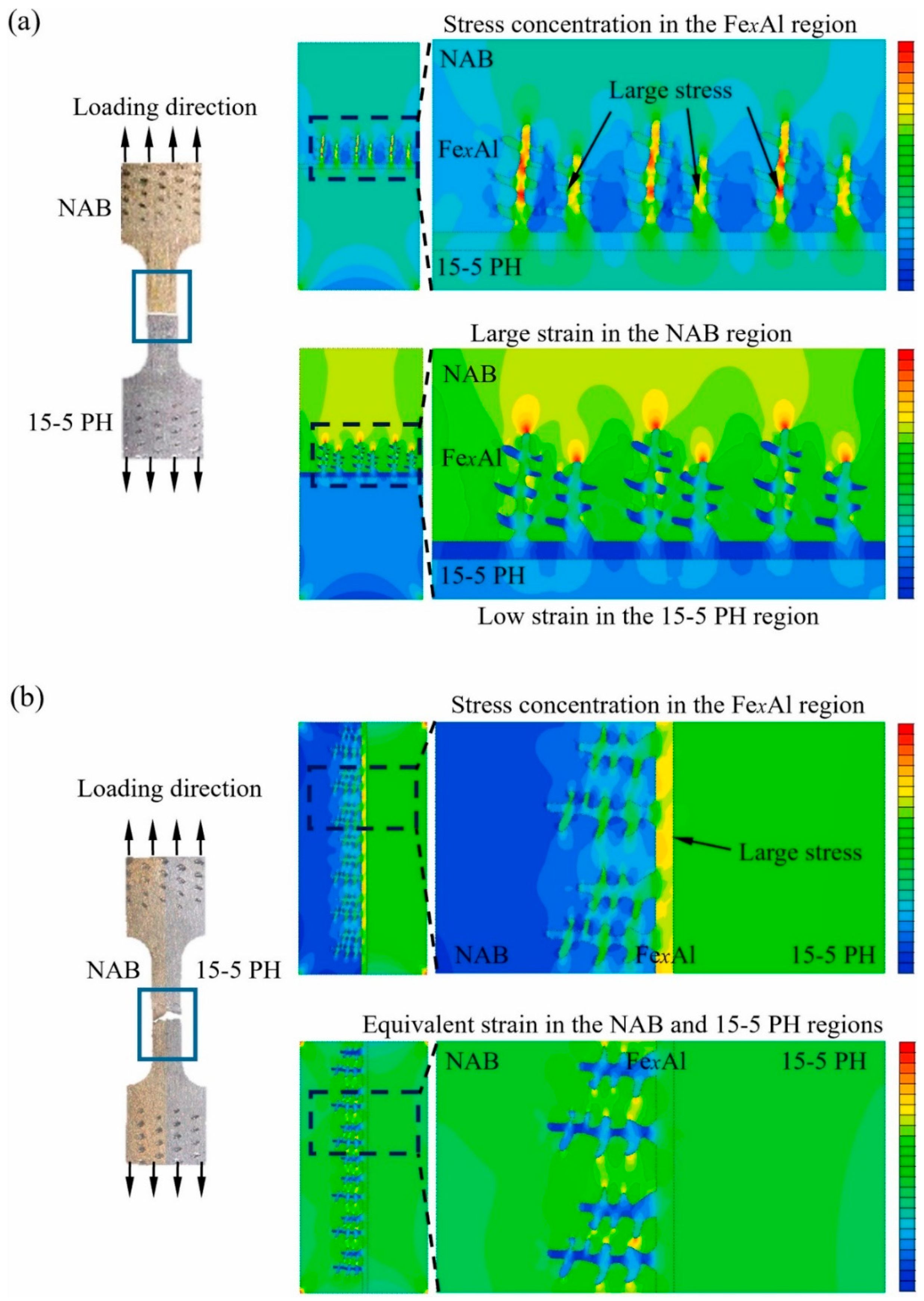
- Li, B.; Han, C.; Lim, C.W.J.; Zhou, K. Interface formation and deformation behaviors of an additively manufactured nickel-aluminum-bronze/15-5 PH multimaterial via laser-powder directed energy deposition. Mater. Sci. Eng. A 2022, 829, 142101. [Google Scholar] [CrossRef]
- Yao, C.-L.; Kang, H.-S.; Lee, K.-Y.; Zhai, J.-G.; Shim, D.-S. A study on mechanical properties of CuNi2SiCr layered on nickel–aluminum bronze via directed energy deposition. J. Mater. Res. Technol. 2022, 18, 5337–5361. [Google Scholar] [CrossRef]
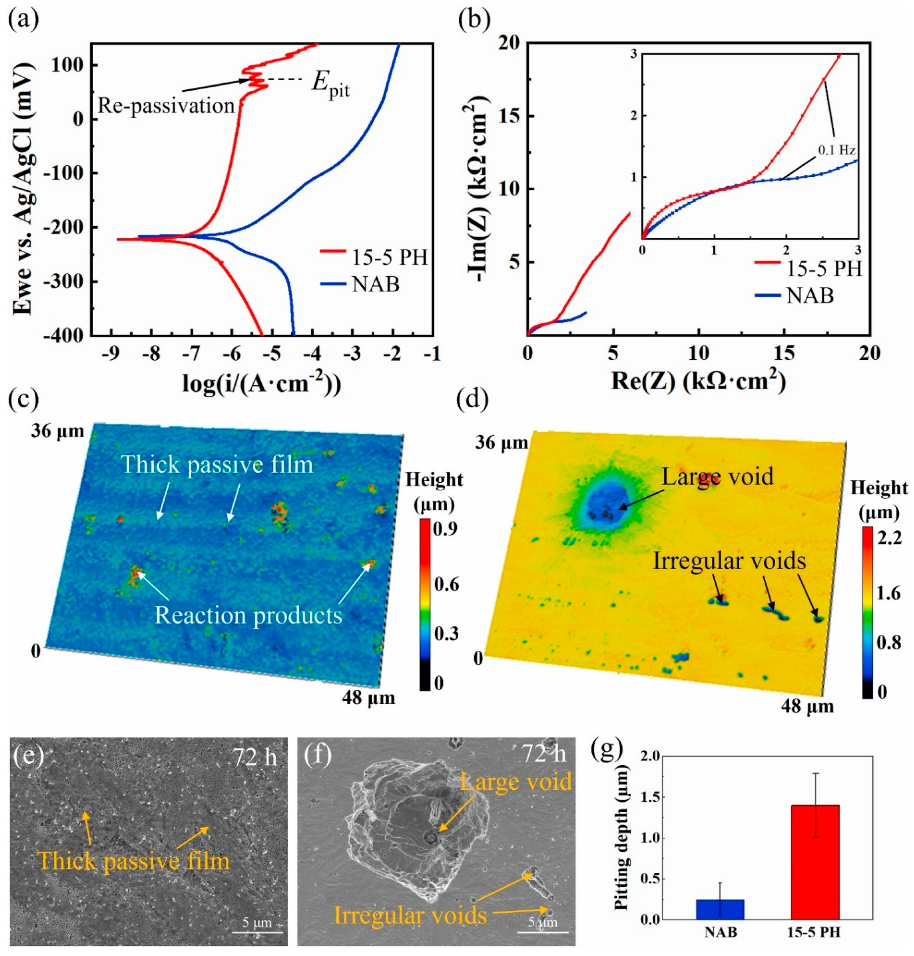
- Yao, C.-L.; Shim, D.-S. Corrosive properties of CuNi2SiCr fabricated through directed energy deposition on a nickel-aluminum bronze substrate. J. Alloys Compd. 2022, 918, 165776. [Google Scholar] [CrossRef]
- Li, B.; Zheng, H.; Han, C.; Zhou, K. Nanotwins-containing microstructure and superior mechanical strength of a Cu–9Al–5Fe–5Ni alloy additively manufactured by laser metal deposition. Addit. Manuf. 2021, 39, 101825. [Google Scholar] [CrossRef]
- Trevisan, D.M.F.; Calignano, F.; Lorusso, M.; Lombardi, M. Selective Laser Melting of Chemical Pure Copper Powders. In Proceedings of the Euro PM 2017: International Powder Metallurgy Congress and Exhibition, Milan, Italy, 1–5 October 2017; pp. 1–6. [Google Scholar]
- Zhang, X.; Zhang, Y.; Tian, B.; Song, K.; Liu, P.; Jia, Y.; Chen, X.; An, J.; Zhao, Z.; Liu, Y.; et al. Review of nano-phase effects in high strength and conductivity copper alloys. Nanotechnol. Rev. 2019, 8, 383–395. [Google Scholar] [CrossRef]
- Weber, L.; Tavangar, R. On the influence of active element content on the thermal conductivity and thermal expansion of Cu–X (X=Cr, B) diamond composites. Scr. Mater. 2007, 57, 988–991. [Google Scholar] [CrossRef]
- Constantin, L.; Fan, L.; Pontoreau, M.; Wang, F.; Cui, B.; Battaglia, J.-L.; Silvain, J.-F.; Lu, Y.F. Additive manufacturing of copper/diamond composites for thermal management applications. Manuf. Lett. 2020, 24, 61–66. [Google Scholar] [CrossRef]
- Hu, Z.; Chen, F.; Lin, D.; Nian, Q.; Parandoush, P.; Zhu, X.; Shao, Z.; Cheng, G.J. Laser additive manufacturing bulk graphene{\textendash}copper nanocomposites. Nanotechnology 2017, 28, 445705. [Google Scholar] [CrossRef]
- Jadhav, S.D.; Dadbakhsh, S.; Vleugels, J.; Hofkens, J.; Van Puyvelde, P.; Yang, S.; Kruth, J.-P.; Van Humbeeck, J.; Vanmeensel, K. Influence of Carbon Nanoparticle Addition (and Impurities) on Selective Laser Melting of Pure Copper. Materials 2019, 12, 2469. [Google Scholar] [CrossRef]
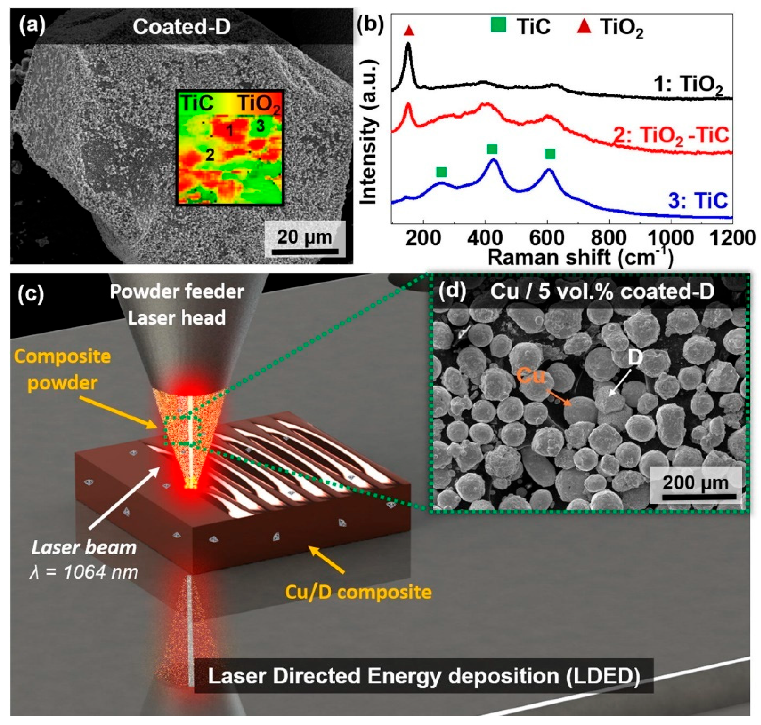
- Lv, X.; Zhan, Z.; Cao, H. Microstructure Evolution and Mechanical Properties of Needle-Like ZrB2 Reinforced Cu Composites Manufactured by Laser Direct Energy Deposition. Micromachines. 2022, 13, 212. [Google Scholar] [CrossRef]
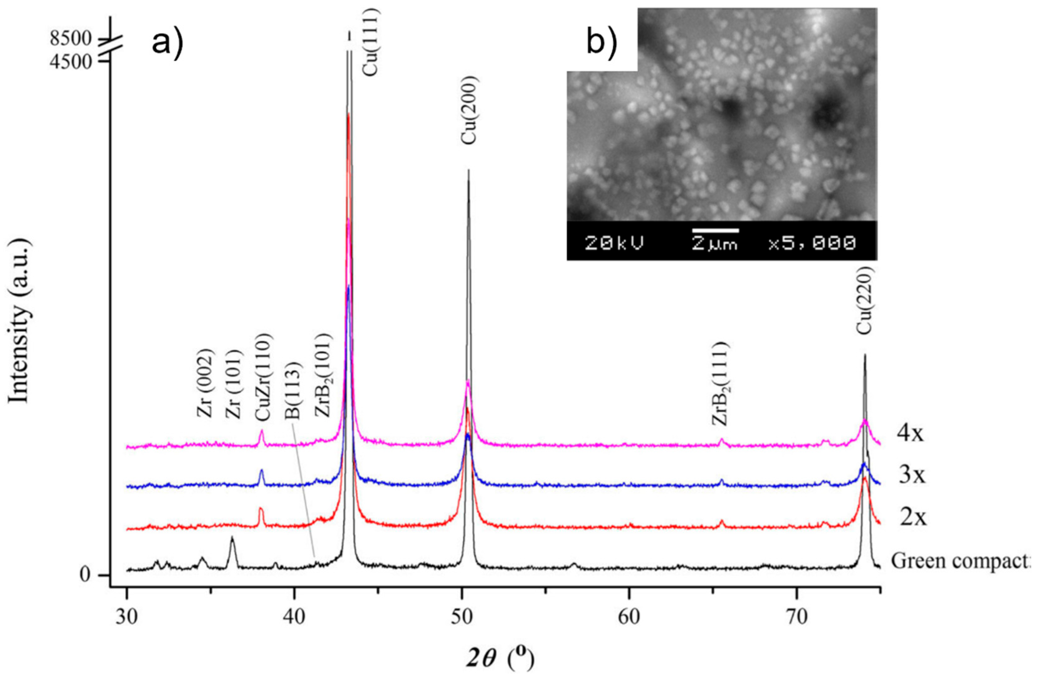
- Stašić, J.; Rajković, V.; Ružić, J.; Božić, D. An investigation on synthesis development of high hardened, high conductivity Cu-Zr and Cu-Zr-ZrB2 alloys through green compact laser sintering. Int. J. Adv. Manuf. Technol. 2015, 80, 1049–1057. [Google Scholar] [CrossRef]
- Pobel, C.R.; Lodes, M.A.; Körner, C. Selective Electron Beam Melting of Oxide Dispersion Strengthened Copper. Adv. Eng. Mater. 2018, 20, 1800068. [Google Scholar] [CrossRef]
- Walker, D.C.; Caley, W.F.; Brochu, M. Selective laser sintering of composite copper–tin powders. J. Mater. Res. 2014, 29, 1997–2005. [Google Scholar] [CrossRef]
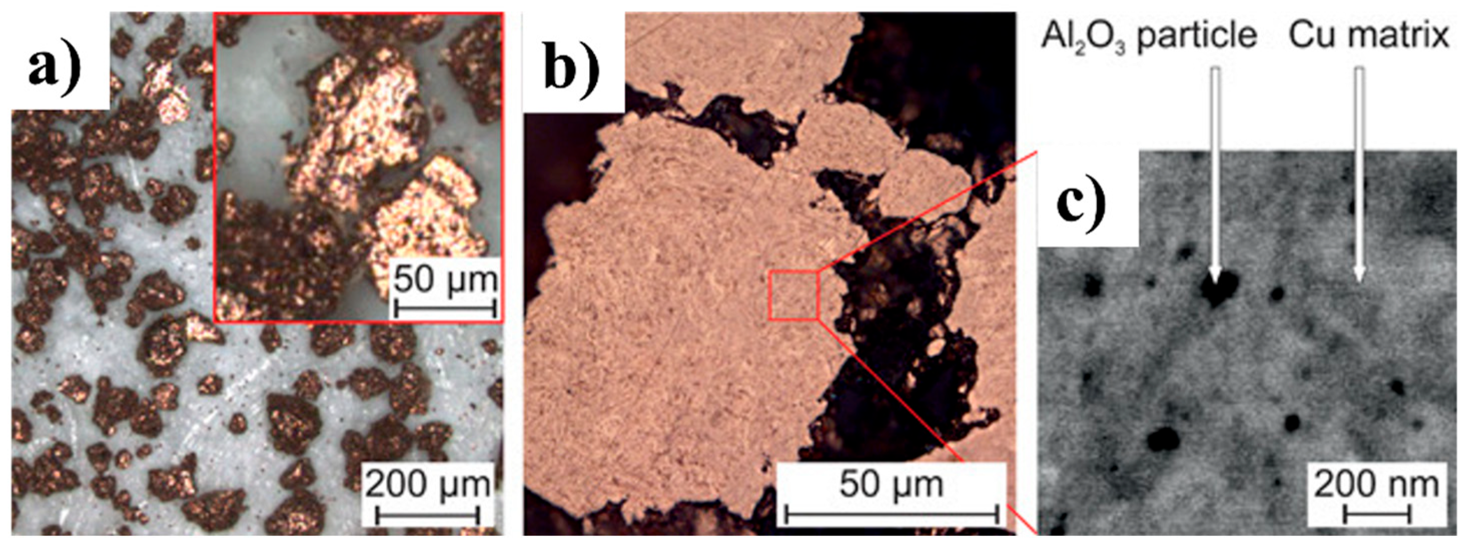
- Li, M.; Huang, J.; Fang, A.; Mansoor, B.; Pei, Z.; Ma, C. Binder jetting additive manufacturing of copper/diamond composites: An experimental study. J. Manuf. Process. 2021, 70, 205–213. [Google Scholar] [CrossRef]
- Sadeghilaridjani, M.; Ladani, L. Location-dependent deformation behavior of additively manufactured copper and copper-carbon nanotube composite. J. Alloys Compd. 2022, 909, 164800. [Google Scholar] [CrossRef]
- Spierings, A.B.; Leinenbach, C.; Kenel, C.; Wegener, K. Processing of metal-diamond-composites using selective laser melting. Rapid Prototyp. J. 2015, 21, 130–136. [Google Scholar] [CrossRef]
- Miracle, D.B. Metal matrix composites—From science to technological significance. Compos. Sci. Technol. 2005, 65, 2526–2540. [Google Scholar] [CrossRef]
- Moghadam, A.D.; Schultz, B.F.; Ferguson, J.B.; Omrani, E.; Rohatgi, P.K.; Gupta, N. Functional Metal Matrix Composites: Self-lubricating, Self-healing, and Nanocomposites-An Outlook. JOM 2014, 66, 872–881. [Google Scholar] [CrossRef]
- Marques, M.T.; Correia, J.B.; Conde, O. Carbon solubility in nanostructured copper. Scr. Mater. 2004, 50, 963–967. [Google Scholar] [CrossRef]
- Daoush, W.M.; Alkhuraiji, T.S.; Khamis, M.A.; Albogmy, T.S. Microstructure and electrical properties of carbon short fiber reinforced copper composites fabricated by electroless deposition followed by powder metallurgy process. Carbon Lett. 2020, 30, 247–258. [Google Scholar] [CrossRef]
- Zhou, W.Y.; Peng, K.; Ran, L.P.; Ge, Y.C.; Yi, M.Z. Effect of Graphitization on the Microstructure and Properties of Mo2C-Modified C/C–Cu Composites. Adv. Eng. Mater. 2016, 18, 1017–1021. [Google Scholar] [CrossRef]
- Shao, W.Z.; Ivanov, V.V.; Zhen, L.; Cui, Y.S.; Wang, Y. A study on graphitization of diamond in copper–diamond composite materials. Mater. Lett. 2004, 58, 146–149. [Google Scholar] [CrossRef]
- Jia, S.Q.; Yang, F. High thermal conductive copper/diamond composites: State of the art. J. Mater. Sci. 2021, 56, 2241–2274. [Google Scholar] [CrossRef]
- Azina, C.; Cornu, I.; Silvain, J.-F.; Lu, Y.; Battaglia, J.-L. Effect of titanium and zirconium carbide interphases on the thermal conductivity and interfacial heat transfers in copper/diamond composite materials. AIP Adv. 2019, 9, 55315. [Google Scholar] [CrossRef]
- Rape, A.; Liu, X.; Kulkarni, A.; Singh, J. Alloy Development for Highly Conductive Thermal Management Materials Using Copper-Diamond Composites Fabricated by Field Assisted Sintering Technology. J. Mater. Sci. 2013, 48, 1262–1267. [Google Scholar] [CrossRef]
- Buhl, S.; Leinenbach, C.; Spolenak, R.; Wegener, K. Microstructure, residual stresses and shear strength of diamond–steel-joints brazed with a Cu–Sn-based active filler alloy. Int. J. Refract. Met. Hard Mater. 2012, 30, 16–24. [Google Scholar] [CrossRef]
- Balandin, A.A.; Ghosh, S.; Bao, W.; Calizo, I.; Teweldebrhan, D.; Miao, F.; Lau, C.N. Superior Thermal Conductivity of Single-Layer Graphene. Nano Lett. 2008, 8, 902–907. [Google Scholar] [CrossRef] [PubMed]
- Lee, C.; Wei, X.; Li, Q.; Carpick, R.; Kysar, J.W.; Hone, J. Elastic and frictional properties of graphene. Phys. Status Solidi 2009, 246, 2562–2567. [Google Scholar] [CrossRef]
- Cu-OF Technical Sheet, 2021. Available online: https://www.eredignutti.it/prodotti/barre-in-ottone/ (accessed on 22 January 2024).
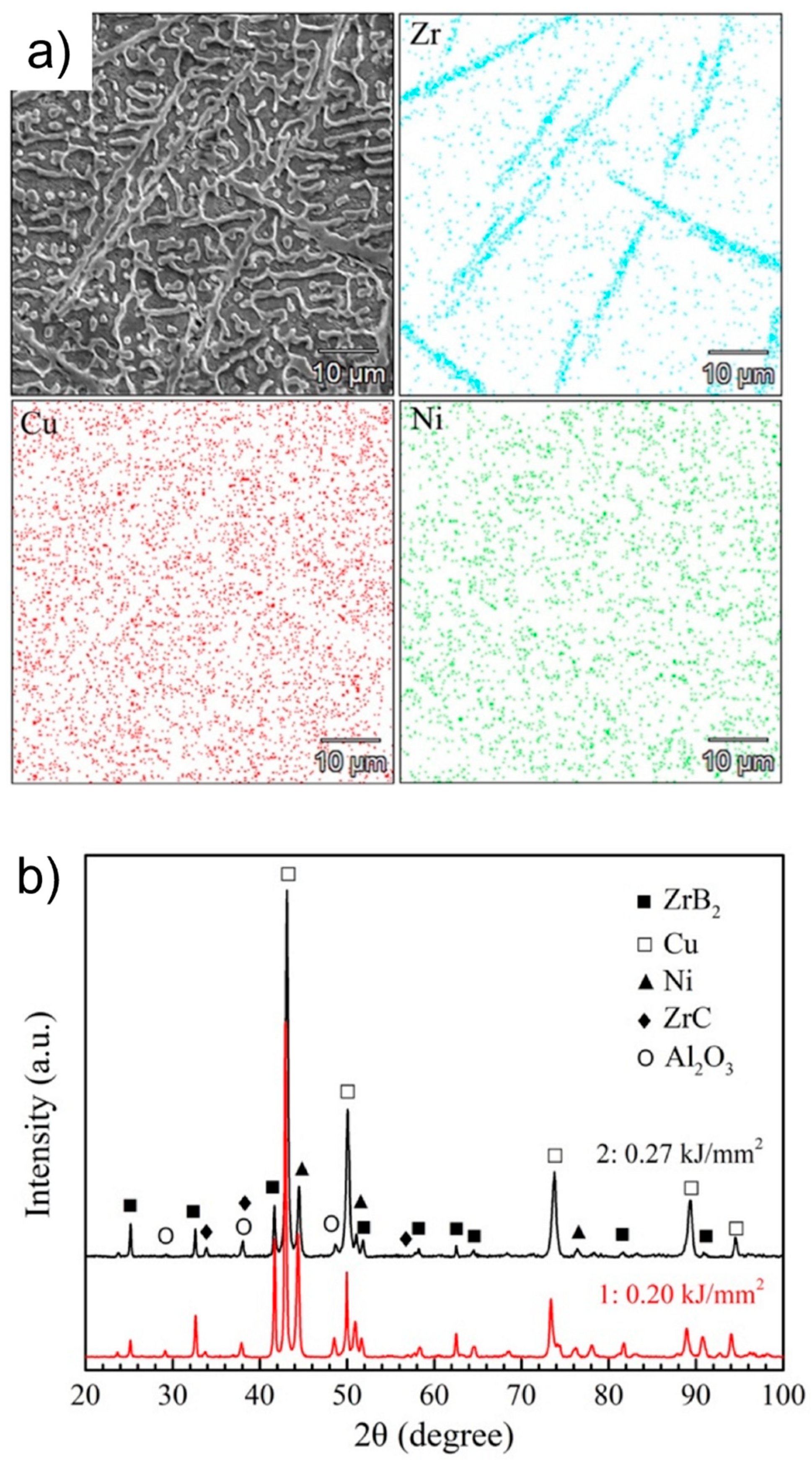
- Zhang, S.; Kang, H.; Li, R.; Zou, C.; Guo, E.; Chen, Z.; Wang, T. Microstructure evolution, electrical conductivity and mechanical properties of dual-scale Cu5Zr/ZrB2 particulate reinforced copper matrix composites. Mater. Sci. Eng. A 2019, 762, 138108. [Google Scholar] [CrossRef]
- Wang, C.; Lin, H.; Zhang, Z.; Li, W. Fabrication, interfacial characteristics and strengthening mechanisms of ZrB2 microparticles reinforced Cu composites prepared by hot-pressed sintering. J. Alloys Compd. 2018, 748, 546–552. [Google Scholar] [CrossRef]
- Ružić, J.; Stašić, J.; Markovic, S.; Raic, K.; Božić, D. Synthesis and Characterization of Cu-ZrB2 Alloy Produced by PM Techniques. Sci. Sinter. 2014, 46, 217–224. [Google Scholar] [CrossRef]
- Sulima, I.; Hyjek, P.; Podsiadło, M. Fabrication of the Zirconium Diboride-Reinforced Composites by a Combination of Planetary Ball Milling, Turbula Mixing and Spark Plasma Sintering. Materials 2021, 14, 4056. [Google Scholar] [CrossRef]
- Passerone, A.; Muolo, M.L.; Novakovic, R.; Passerone, D. Liquid metal/ceramic interactions in the (Cu, Ag, Au)/ZrB2 systems. J. Eur. Ceram. Soc. 2007, 27, 3277–3285. [Google Scholar] [CrossRef]
- Kruth, J.P.; Schueren, B.; Bonse, J.; Morren, B. Basic powder metallurgical aspects in selective metal powder sintering. CIRP Ann. 1996, 45, 183–186. [Google Scholar] [CrossRef]


| Alloy | Pretreatment | Process Parameters | Post-Treatment | Ref. |
|---|---|---|---|---|
| Cu-0.5Cr (wt.%) | None |
|
| [60] |
| Cu-0.5Cr (wt.%) with an average particle size of 35.5 μm | None |
|
| [61] |
| Cu-1.3Cr Cu-2.5Cr (wt.%) with an average particle size of 24 μm | None |
|
| [62] |
| CuCr0.3 with an average particle size of 33.7 μm |
|
|
| [63] |
| Cu-Cr0.89 with an average particle size of 39.9 μm |
|
|
| [64] |
| Cu-Cr1 with an average particle size of 38.5 μm |
|
|
| [65] |
| Cu-0.8Cr with an average particle size of 30 μm |
|
|
| [66] |
| Cu-20Cr Cu-25Cr with an average particle size of 40–50 μm |
|
|
| [67] |
| Alloy | Powder Size | Pretreatment | Process Parameters | Ref. |
|---|---|---|---|---|
| Cu76-Ni14.8-Sn7-Pb1.6 | 20 μm | 80 °C preheating of steel base plate |
| [86] |
| Cu-5Ni Cu-10Ni Cu-15Ni | 20–43 μm | 80 °C preheating of steel base plate |
| [87] |
| Cu-19Ni | 40 μm | Not reported |
| [88] |
| Cu-22.82Ni-4.72Sn-1.43P | Not reported | Not reported |
| [89] |
| Parameter | Value |
|---|---|
| Voltage | 18 V |
| Current | 80 A |
| Feeding speed | 5 m·min−1 |
| Printing speed | 14 mm s−1 |
| Contact tip for working distance | 15 mm |
| Gas flow rate | 10–15 L·min−1 |
| Interlayer temperature | ≤150 °C |
| Overlap rate | 50% |
| Element | Blend1 | Blend2 | Blend3 | Blend4 |
|---|---|---|---|---|
| Cu (wt.%) | 0 | 25 | 50 | 75 |
| Ni (wt.%) | 100 | 75 | 50 | 25 |
| Element | Blend1 | Blend2 | Blend3 | Blend4 | Blend5 |
|---|---|---|---|---|---|
| Copper (wt.%) | 0 | 10 | 30 | 50 | 70 |
| Delero-22 (wt.%) | 100 | 90 | 70 | 50 | 30 |
| Sample | Laser Power (W) | Scan Speed (mm·s−1) | Powder Feed Rate (g·min−1) | Stepover Distance (mm) | Density (g·cm−3) |
|---|---|---|---|---|---|
| B1S1 | 800 | 550 | 5 | 1.05 | 8.25 ± 0.20 |
| B1S2 | 800 | 550 | 5 | 1.05 | 8.34 ± 0.02 |
| B2S3 | 800 | 500 | 5 | 1.05 | 8.36 ± 0.16 |
| B2S4 | 800 | 550 | 5 | 0.95 | 8.46 ± 0.13 |
| AM Process | Matrix | Reinforcement | Maximum Relative Density (%) | Process Parameters | Reflectance (%) | Maximum Thermal Conductivity (W/m·K) | IACS (%) | Maximum Tensile Strength (MPa) | Maximum Vickers Hardness (HV) | Ref. |
|---|---|---|---|---|---|---|---|---|---|---|
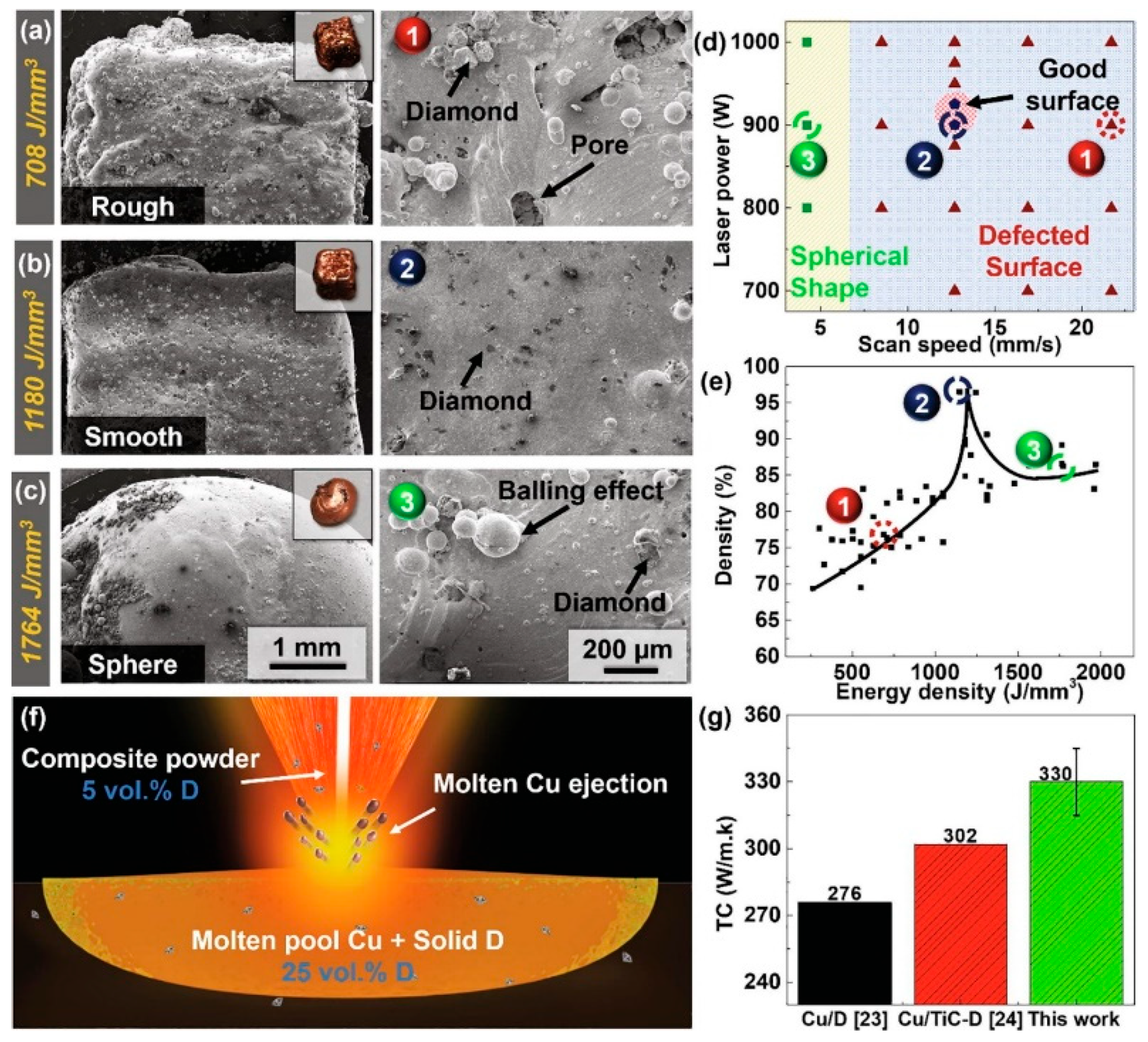
| DED | Pure Cu | Diamond (5 vol%) | 96 | Proper scan speed: 12.7 mm/s Hatch spacing: 0.3 mm Proper laser power: 900 W Layer thickness: 0.2 mm | - | 330 | - | - | - | [175] |
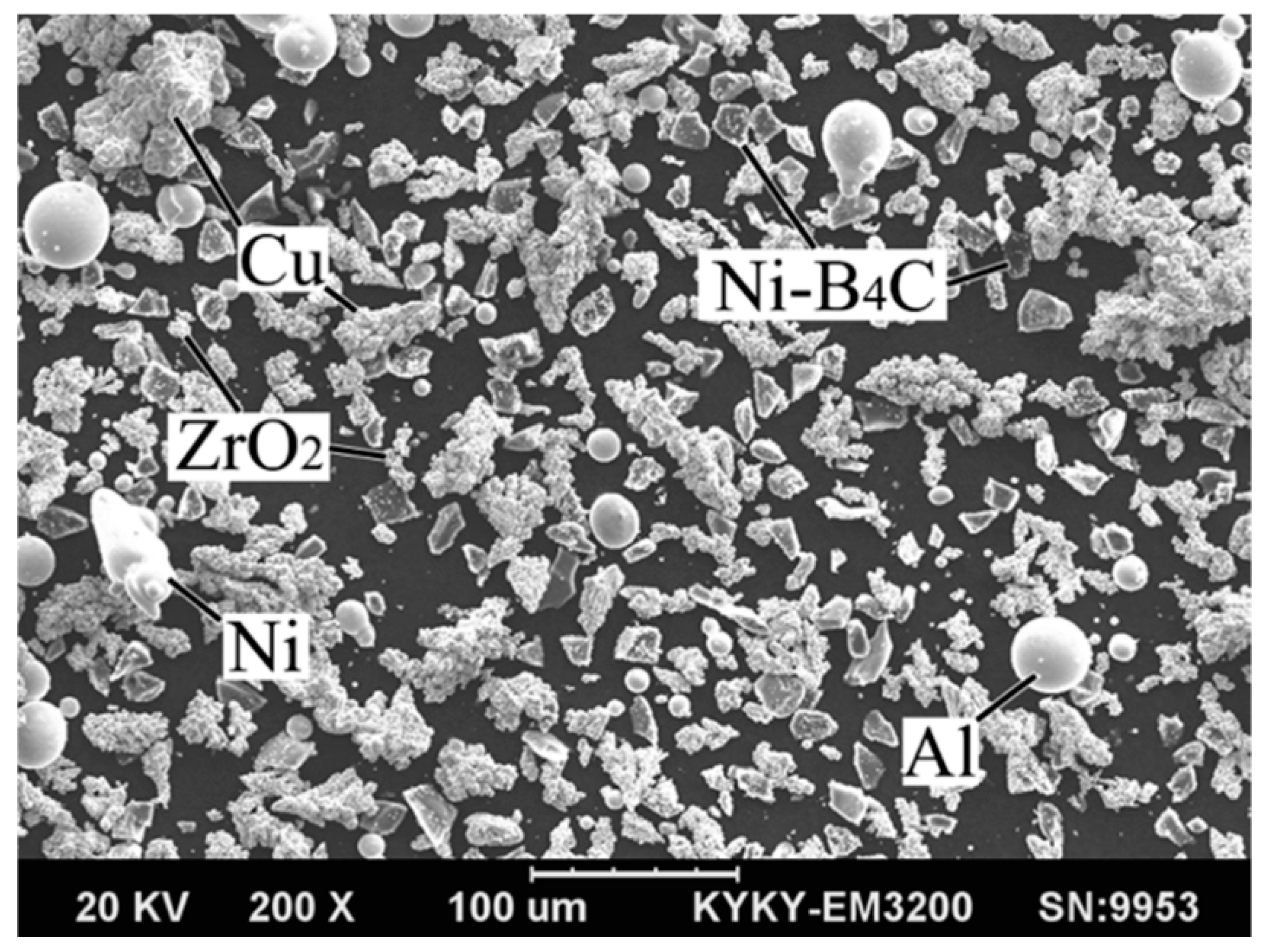
| DED | Cu-13.96wt.%Ni- 10.41wt.%ZrO2- 3.04wt.%Al- 2.59wt.% Ni-B4C | ZrB2 | - | Proper scan speed: 3 mm/s Proper laser power: 1800 W | - | - | - | 535.24 | - | [178] |
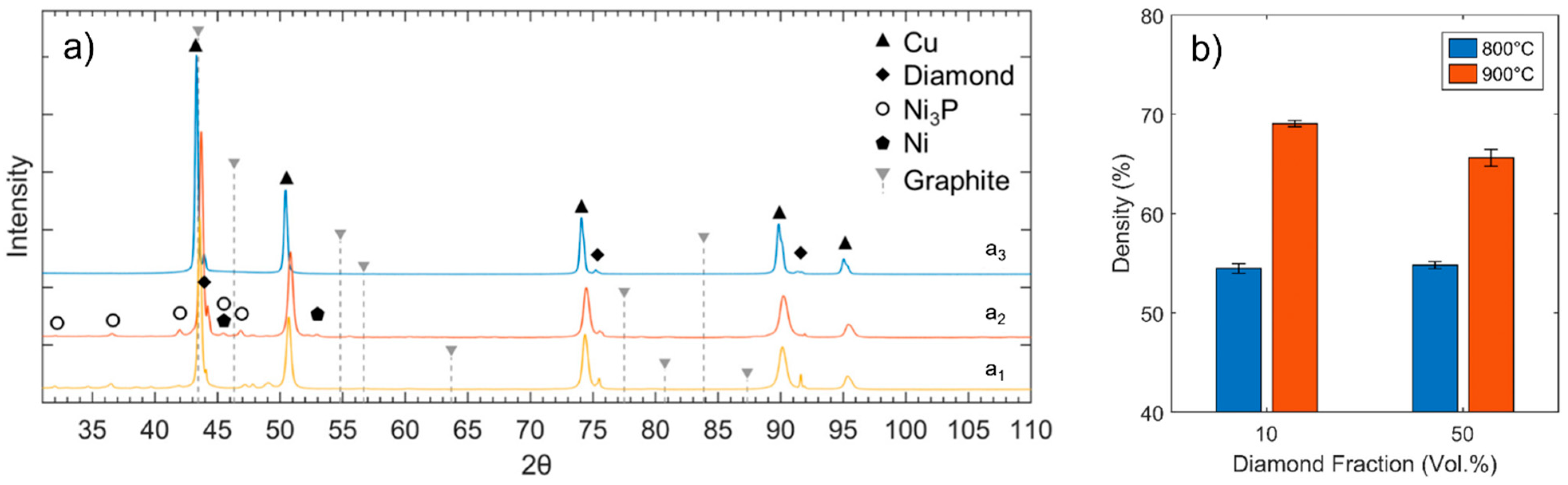
| BJT | Pure Cu | Diamond (10 and 50 vol%) | 45.05 | Traverse speed: 30 mm/s Rotational speed: 500 rpm Sintering process: 2h 800 °C and 900 °C | - | - | - | - | - | [182] |
| L-PBF | Pure copper | GO (0.1 wt.%) | 90.8 (83.1 for pure Cu) | Proper scan speed: 600 mm/s Hatch spacing: 0.06 mm Proper laser power: 175 W | 57.1 (84.1 for pure Cu) | 267.93 | 63.83 | 164.37 | - | [23] |
| L-PBF | Pure copper | CNPs (0.1 wt.%) | 98 | Proper scan speed: 400 mm/s Hatch spacing: 0.12 mm Proper laser power: 725 W Layer thickness: 0.03 mm | 33 (71 for pure copper) | 164.2 * | 39.2 | 125 | - | [177] |
| L-PBF | CuCr0.3 | CNPs (0.05 wt.%) | 98.6 | Proper scan speed: 300 mm/s Hatch spacing: 0.09 mm Proper laser power: 600 W Layer thickness: 0.03 mm | 44 (58 for pure CuCr0.3) | 326 * | 78 | 271 | - | [63] |
| L-PBF | Pure copper | CNTs (0.5 wt.%) | ~85 | Proper scan speed: 47 mm/s Hatch spacing: 0.10 mm Proper laser power: 93 W | - | - | - | - | ~112 | [183] |
| L-PBF | Cu- 14.4wt%Sn-10.2wt.%Ti- 1.5wt.%Zr | Diamond (10 and 20 vol%) | 98.5 | Hatch spacing: 0.08 mm Proper laser power: 100 W Layer thickness: 0.03 mm | - | - | - | - | - | [184] |
| SLS | Pure copper | Graphene nanoplatelets (1.9g Cu:0.1g C) | - | Proper scan speed: 2 mm/s Step size: 0.25 mm Proper laser power: 70 W Frequency: 50000 Hz | - | - | - | 135 | [176] | |
| SLS | Cu-4.1wt.%Zr-1.1wt.%B | ZrB2 | 98 | Proper scan speed: 0.5 mm/s Step size: 0.5 mm Frequency: 3 Hz Pulse duration: 10 ms | - | - | 42 | - | [179] | |
| SLS | Cu-10wt.%Sn | Sn | 36 | Proper scan speed: 1.5 mm/s Proper laser power: 90 W Frequency: 1 Hz | - | - | 0.2 | - | [181] | |
| EBM | Pure copper | Al2O3 (2.28wt.%) | - | Proper scan speed: 3000 mm/s beam current: 1.67–26.67 ×10⁻³ A Layer thickness: 0.05 mm | - | - | - | - | - | [180] |
Disclaimer/Publisher’s Note: The statements, opinions and data contained in all publications are solely those of the individual author(s) and contributor(s) and not of MDPI and/or the editor(s). MDPI and/or the editor(s) disclaim responsibility for any injury to people or property resulting from any ideas, methods, instructions or products referred to in the content. |
© 2024 by the authors. Licensee MDPI, Basel, Switzerland. This article is an open access article distributed under the terms and conditions of the Creative Commons Attribution (CC BY) license (https://creativecommons.org/licenses/by/4.0/).
Share and Cite
Vahedi Nemani, A.; Ghaffari, M.; Sabet Bokati, K.; Valizade, N.; Afshari, E.; Nasiri, A. Advancements in Additive Manufacturing for Copper-Based Alloys and Composites: A Comprehensive Review. J. Manuf. Mater. Process. 2024, 8, 54. https://doi.org/10.3390/jmmp8020054
Vahedi Nemani A, Ghaffari M, Sabet Bokati K, Valizade N, Afshari E, Nasiri A. Advancements in Additive Manufacturing for Copper-Based Alloys and Composites: A Comprehensive Review. Journal of Manufacturing and Materials Processing. 2024; 8(2):54. https://doi.org/10.3390/jmmp8020054
Chicago/Turabian StyleVahedi Nemani, Alireza, Mahya Ghaffari, Kazem Sabet Bokati, Nima Valizade, Elham Afshari, and Ali Nasiri. 2024. "Advancements in Additive Manufacturing for Copper-Based Alloys and Composites: A Comprehensive Review" Journal of Manufacturing and Materials Processing 8, no. 2: 54. https://doi.org/10.3390/jmmp8020054