Article

Designed on 0.18 μm CMOS Process Small Size Broadband Millimeter Wave Chip Antenna

Department of Electronic Engineering, National Taipei University of Technology, Taipei 10608, Taiwan
*
Author to whom correspondence should be addressed.
Inventions 2023, 8(3), 64; https://doi.org/10.3390/inventions8030064
Submission received: 5 April 2023 / Revised: 21 April 2023 / Accepted: 24 April 2023 / Published: 25 April 2023

Abstract

:
This paper proposes a small-size broadband triangular monopole chip antenna for millimeter wave band applications. Process using 0.18 μm CMOS process and antenna design using Met-al_6. Triangular patch design and feed line length analysis to achieve a better reflection coefficient and also dig three circular slots at the grounding point to achieve better impedance matching. The operating frequency of the chip antenna is 62–100 GHz below the reflection coefficient −10 dB standard, with a fractional bandwidth of 54%. The maximum gain is −0.4 dBi at 64 GHz. The efficiency is 40.9%. The overall chip size is 1.2 × 1.2 (mm2). After measurement and verification, the proposed antenna reflection coefficient is similar to the simulation trend and has better resonance. The chip antenna frequency range proposed in this article covers the 5G NR FR2 frequency band. The proposed chip antenna can be applied in related fields such as the Internet of Things, Industry 4.0, and biomedical electronics.

1. Introduction

The increasing demand for wireless connections has led to data traffic congestion on the traditional microwave spectrum. In response to such huge demand, the Third Generation Partnership Plan (3GPP) has expanded the frequency band of 5G New Radio (5G NR) to FR1 (0.4–7.1 GHz) and FR2 (24.2–52.6 GHz) to achieve higher connectivity, higher data rates, ultra-low latency, higher energy efficiency, and higher spectral efficiency to process these data and information [1]. Under the network coverage of the fifth-generation mobile communication, billions of physical devices worldwide are connected to the Internet and transmit a large amount of data and information through networks independent of human behavior [2,3]. The development of the Internet of Things has promoted the rapid growth of smart homes, smart cities, smart grids, industrial automation, and healthcare, and environment and traffic monitoring. Even if the novel coronavirus epidemic suddenly occurred in recent years, the demand for such a large number of equipment did not show a downward trend [4,5]. In recent years, with the transformation of mobile communication networks, more and more research has been conducted on the frequency bands of millimeter wave communication systems, including n257 (26.5–29.5 GHz), n258 (24.2–27.5 GHz), n259 (39.5–43.5 GHz), n260 (37–40 GHz), and n261 (27.5–28.3 GHz). Implementing high-performance, low-cost, and low-power transceivers has become an important research topic [6]. In addition to the above frequency bands, scientists are also actively studying the 60 GHz and 77 GHz communication frequency bands and applying them in the fields of industry, medical treatment, and automotive radar [7]. The sub-terahertz frequency band above 100 GHz is also attracting attention and will apply to physical systems, such as autonomous vehicles, robotic networks, virtual reality, or applications, such as intelligent sensing, imaging, defect detection, and short-range wireless communication [8,9].
In the past two decades, advanced process technology has led to a breakthrough in the growth of integrated circuits. Billions of transistors can be manufactured on a few square millimeters of wafer and the precision of manufacturing technology is becoming increasingly mature [10]. Due to the improvement in the high-frequency characteristics of chip antennas through scaling, complementary metal oxide semiconductors (CMOS) have become a viable manufacturing method for chip antennas and can integrate a complete chip antenna system on a single chip through CMOS processes, further enhancing the competitiveness of the system [11,12]. However, the radiation efficiency and performance of chip antennas are still their disadvantages. In typical process of CMOS, the low resistivity and high dielectric coefficient of the silicon substrate will seriously cause the loss of the antenna and the silicon substrate will absorb most of electromagnetic waves, greatly reducing the radiation efficiency of the antenna [13]. However, compared to traditional antenna systems, chip antenna systems still have higher bandwidth, better integration advantages, and lower power consumption performance. In addition, as the most critical part of the system, the chip antenna eliminates parasitic effects and uncertainties on the circuit caused by additional connections. It can be directly connected to the circuit without requiring additional matching networks, providing designers with a more flexible design approach and facilitating chip layout [14,15]. Such a process has been applied in the frequency band of novel communication applications, such as millimeter wave and terahertz. The emergence of chip antennas has brought enormous potential to communication technology, playing an important role in the future Internet of Things [16,17].
In recent years, there has been extensive research in the field of millimeter wave chips, with different orientations and implementations. For example, resonance analysis [18,19,20,21], the introduction of artificial magnetic conductors [22,23], the design of integration with printed circuit boards [24,25], the design of integrated circuits [26], and miniaturization [27]. The influence of the number of twists and turns of a monopole antenna on the operating frequency is shown through simulation results. In reference [18], resonance is achieved at 28 GHz and 60 GHz, achieving the goal of dual frequency. In addition, considering the chip layout, a packaging substrate was selected and placed below the silicon substrate to generate constructive radiation at two frequencies, enhancing antenna gain and efficiency. Reference [19], coupled the feed antenna by adding a square resonant ring, which improved the gain of 7 dBi at 85 GHz and measured a maximum gain of 1.61 dB at 81.5 GHz. Reference [20] analyzed the dual ring antenna and analyzed the influence of dielectric resonator size on the radiation performance and gain of the antenna. In addition, a reflective plate has also been added to the design of the Yagi antenna, which has increased the gain by 0.8 dBi [21]. By conducting resonance analysis on the antenna, the best method to improve antenna performance can be determined. By adjusting the impedance and bandwidth through the use of parasitic capacitance generated by double-layer artificial magnetic conductors, it has been confirmed through measurement that the bandwidth has increased to 5.8 GHz and a consistent input impedance has been obtained [22]. Reference [23] analyzed and compared different artificial magnetic conductor units, and the results showed that the proposed (back-to-back E-shaped, B2BE) architecture had the best reflection coefficient (75–125 GHz) and was applied to antennas. With the assistance of artificial magnetic conductors, the gain and efficiency of chip antennas can be improved to a certain extent. However, in recent years, there have been studies and designs that integrate printed circuit boards and active circuits, which can overcome the disadvantages of low gain and low efficiency of chip antennas. For example, the use of air-filled substrate synthesis waveguide technology combined with chip antennas results in the better resonance of chip antenna radiation, with an efficiency improvement of over 90% [24] Alternatively, integrate the chip antenna with the active circuit and embed it into the printed circuit board to improve the overall antenna gain [25]. Reference [26] introduced a switching circuit in the chip antenna, which achieved an overall bandwidth of 53.4% in two operating states. Switching circuits can increase the operating mode of chip antennas and improve bandwidth performance. By using a hexagonal grid structure to reduce the size, [27] analyzed the angle of the grid to optimize impedance matching, and proposed a miniaturized broadband monopole antenna for the W-band. Additionally, the capacitance effect between the sixth layer of metal and the first layer of metal was utilized to achieve broadband, with an antenna bandwidth of 31.5%. Chip antennas can be miniaturized using different architectures, and the capacitance effect between metal layers can be used to enhance bandwidth.
In this article, it is proposed that 1 × 2 broadband monopole chip antennae use 0.18 μm CMOS manufacturing process with an antenna area of 1.2 × 1.2 (mm2), which improves antenna radiation performance through array mode. The proposed triangular patch antenna design and circular slot holes enhance bandwidth performance. Measurements have verified that the bandwidth is 57.6–93.8 GHz, with a fractional bandwidth 54%, below the reflection coefficient −10 dB standard. Additionally, the proposed antenna has −0.4 dBi gain at 64 GHz. The antenna radiation efficiency is 40%. The frequency band covers the millimeter wave frequency band of 5G NR FR2. The explanation framework of this article is as follows: the second chapter explains the topology, simulation results, evolution, and parameter analysis of the proposed antenna. The third chapter compares the results of measurement and simulation to illustrate the differences between measurement and simulation. The fourth chapter describes the performance comparison with the recent literature and proposes the advantages of this antenna. Finally, in fifth chapter, the performance and characteristics of this antenna are summarized.

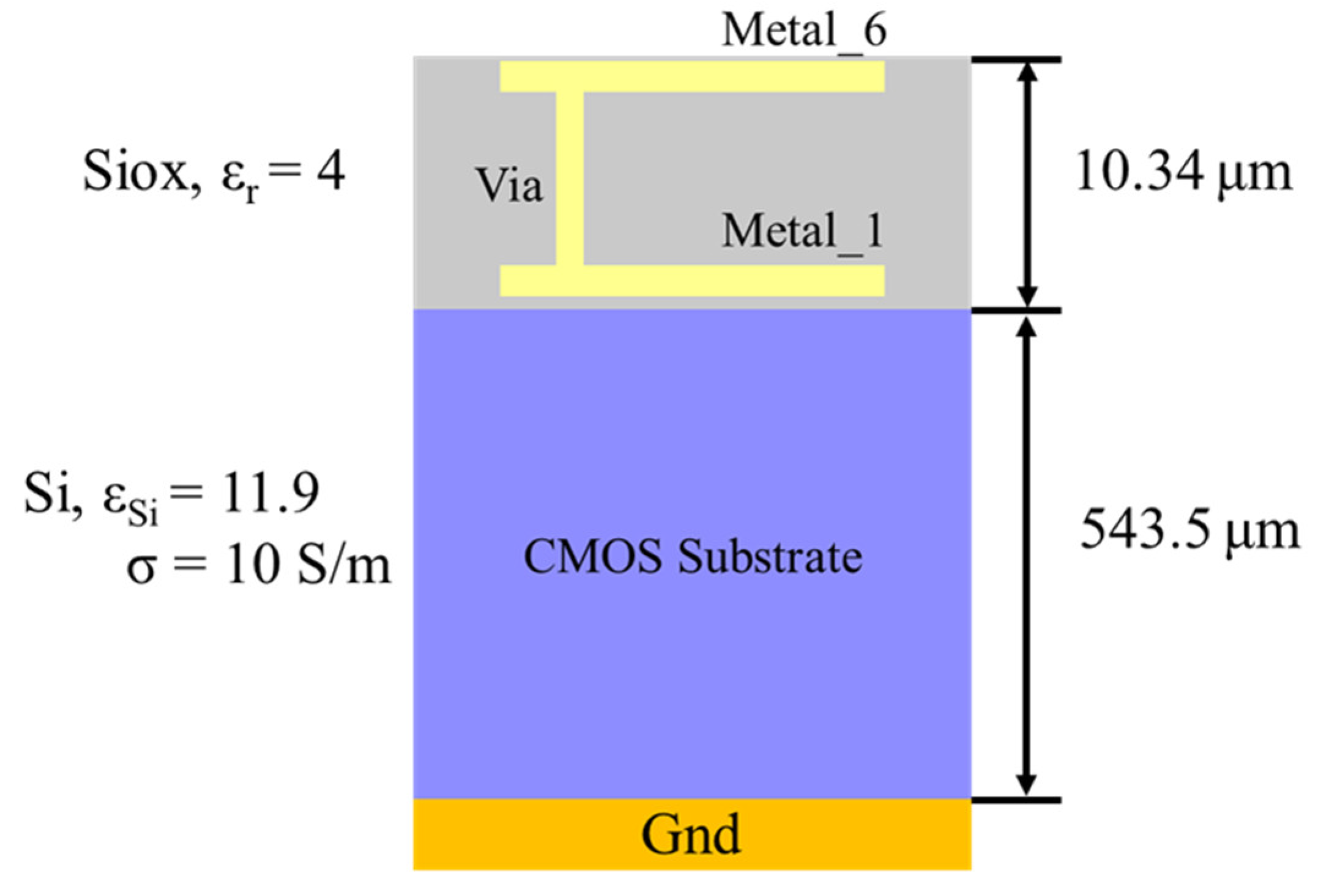
2. Materials and Methods

Figure 1 is a top view of the chip antenna proposed in this article, designed using a 0.18 μm CMOS process, which shown as Figure 1. This antenna composed of two triangular patches and a 1 × 2 microstrip line power divider. We used a GSG feed structure at the feed line, which is connected to Metal_1. For grounding, adding a circular groove design at the grounding point can achieve better impedance matching. The design of the trenching on the triangular patch in the picture is to comply with the limitations of the design rules. Figure 2 shows the 0.18 μm CMOS process stack architecture, with a silicon dioxide layer thickness of 10.34 μm, and a dielectric coefficient of 4. The silicon substrate thickness is 543.5 μm and the dielectric coefficient is 11.9. The triangular patch antenna and microstrip line power divider are implemented using a sixth metal layer.
Figure 3 and the geometric diagram of the chip antenna proposed in this article. Table 1 shows the dimensions of the geometric parameters of each part of the chip antenna. The reflection coefficient, gain, and efficiency of the chip antenna are simulated, shown in Figure 4, Figure 5 and Figure 6, respectively. The minimum reflection coefficient of chip antenna simulated at 64 GHz, with bandwidth of 57.6–93.8 GHz at the −10 dB standard. The maximum gain and efficiency are −0.4 dBi and 40.9%, respectively, at 64 GHz.

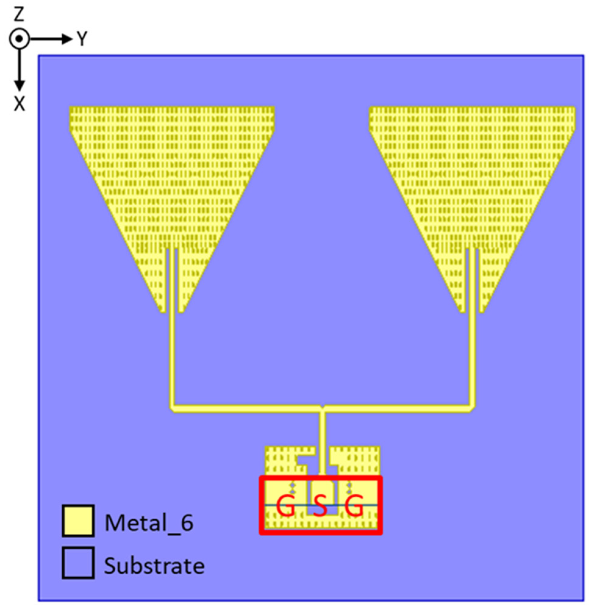
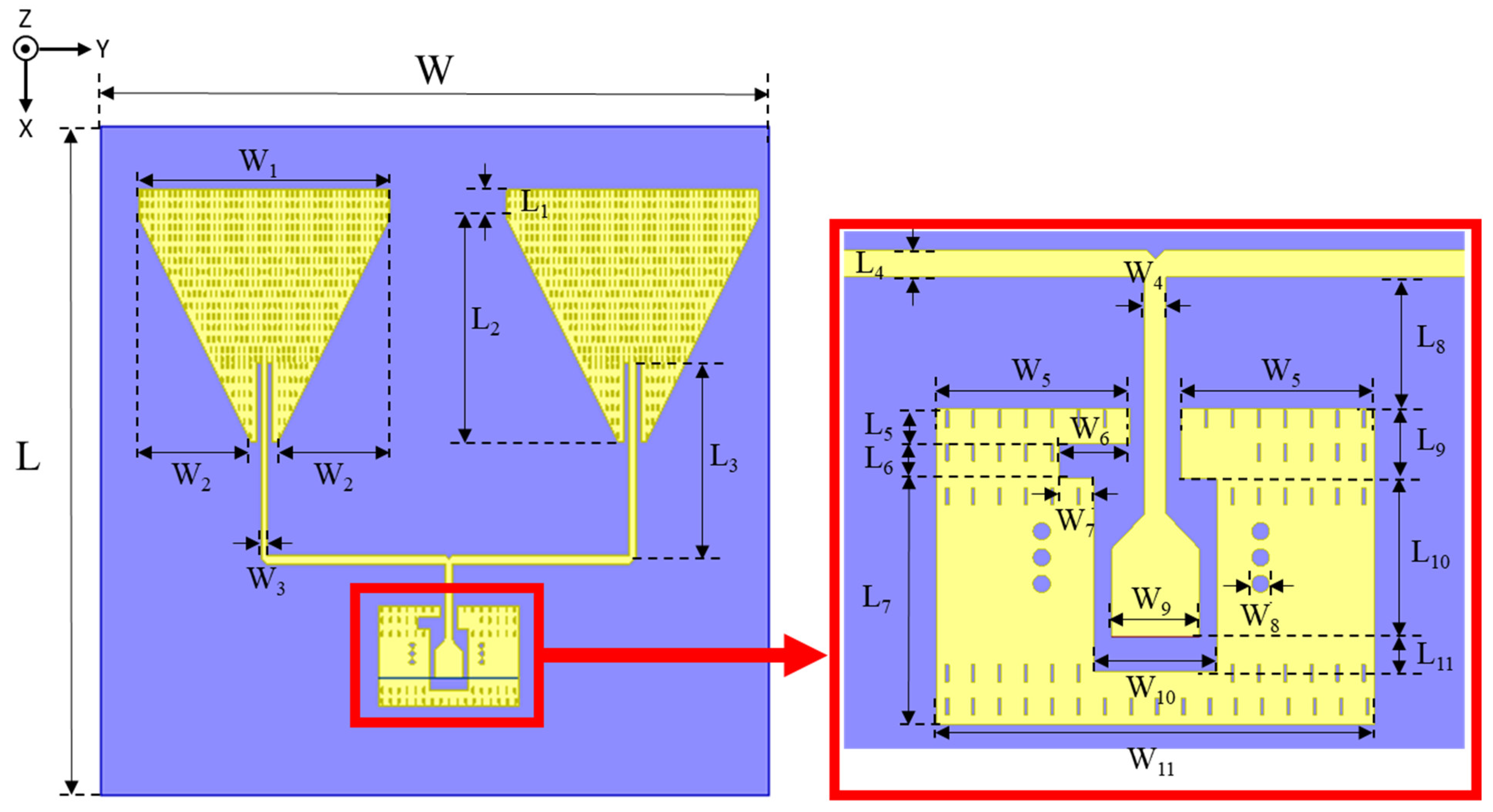
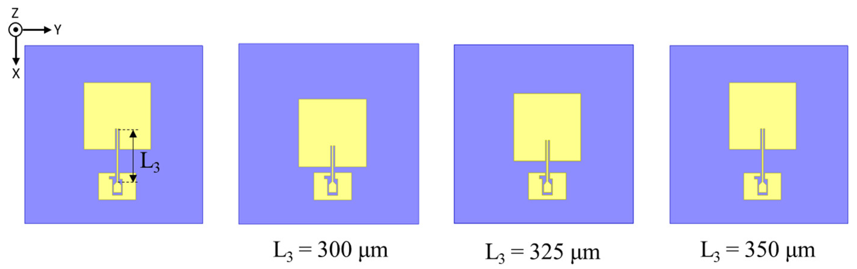
2.1. Parameter Analysis of Antenna Feed Line

First, this paper analyzes the parameters of the feed line length L3 for a single patch antenna. Figure 7 shows three different lengths of square monopole patch antennas, each 300 μm, 325 μm, and 350 μm, respectively. The results are shown in Figure 8, with the reflection coefficient of −10 dB as the bandwidth standard. When the feed line length L3 is 300 μm, the bandwidth range is 88.6–94.5 GHz. When L3 is 325 μm, the bandwidth range is 85.7–97.5 GHz. When the L3 length is 350 μm, the bandwidth range is 83.1–100 GHz. From this parameter simulation, it can be seen that when the feed length is 350 μm, there is an optimal bandwidth range.

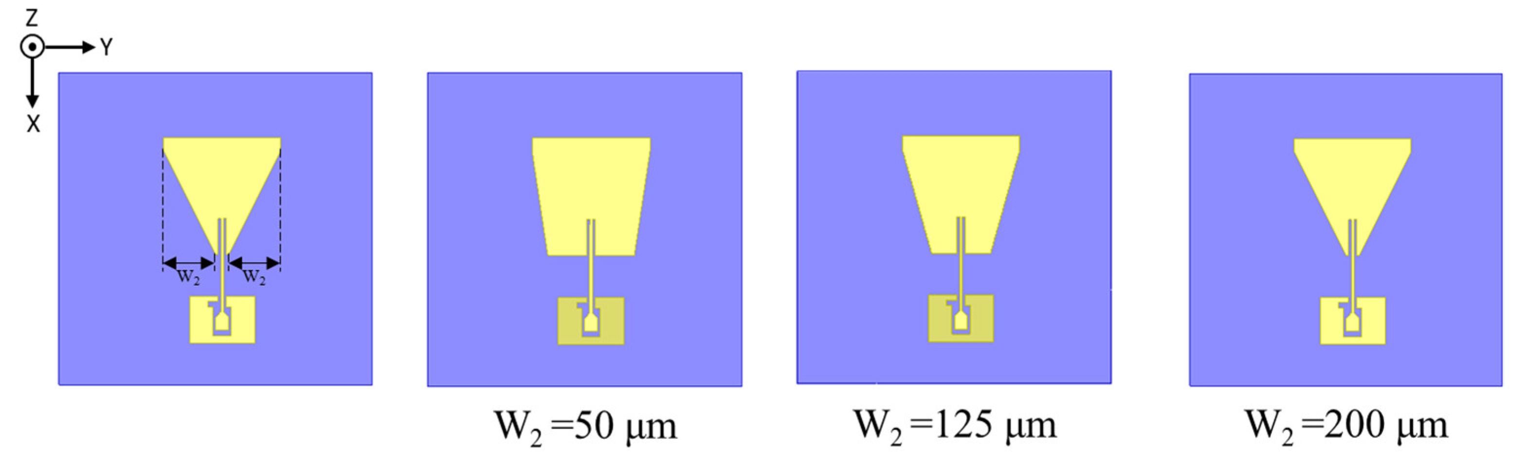
2.2. Parameter Analysis of Triangular Patch

Next, we analyze the antenna parameter W2, as shown in Figure 9, when W2 is equal to 50, 125, and 200 μm, respectively. The simulation results are shown in Figure 10. When the reflection coefficient is −10 dB and the parameter W2 is equal to 50 μm, the bandwidth range is 78.2–86.7 GHz. When W2 is equal to 125 μm, the bandwidth range is from 75.5–87.7 GHz. When W2 is equal to 200 μm, the bandwidth range is 73.8–89.1 GHz. From this parameter simulation, it can be seen that when the antenna parameter W2 is equal to 200 μm, there is the best bandwidth performance.

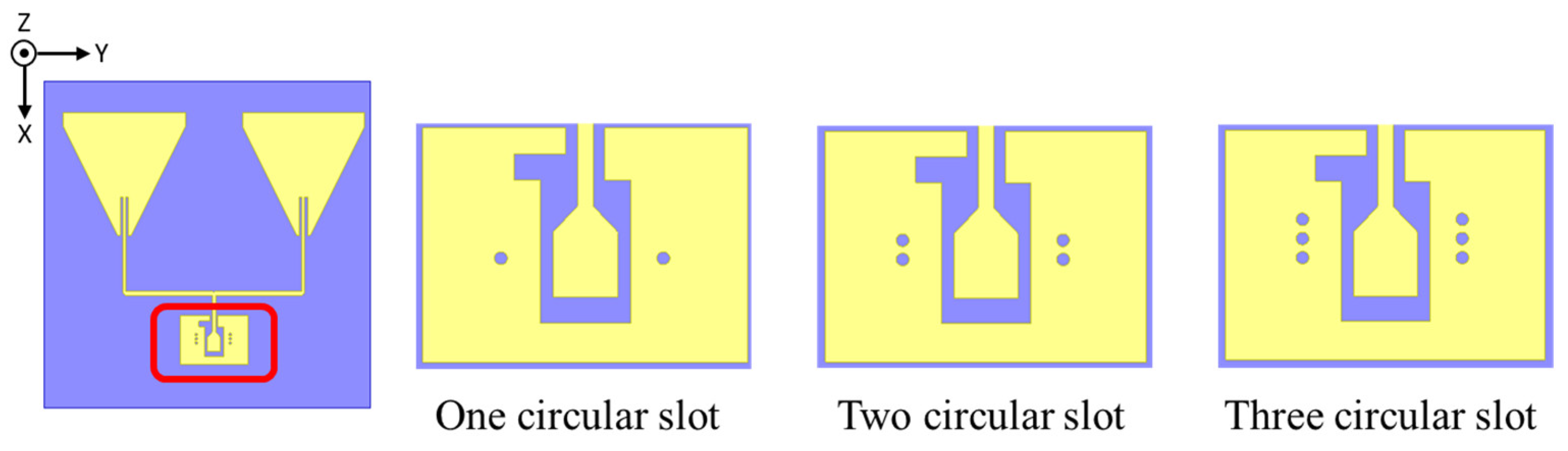
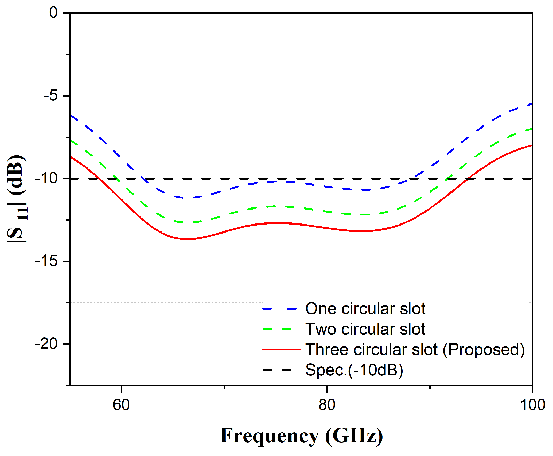
2.3. Parameter Analysis of Different Numbers of Circular Slot

In this article, the original triangular patch antenna is transmitted through 1 × 2 power divider of 2 expands it into a 1 × 2 array antenna and performs parameter analysis by digging a circular slot in the ground. As shown in Figure 11, 1, 2, and 3, circular slot holes were dug at the ground, and the bandwidth range was observed at a reflection coefficient of −10 dB. The results are shown in Figure 12. When digging a circular slot hole, the bandwidth range is between 62.2 GHz and 88.1 GHz. When digging two circular slots, the bandwidth range is 59.6–91.7 GHz. When digging three circular slots, the bandwidth range is from 57.9–93.7 GHz. From the simulation results, it can be seen that the optimal bandwidth range is achieved when three circular slots are dug at the grounding point.

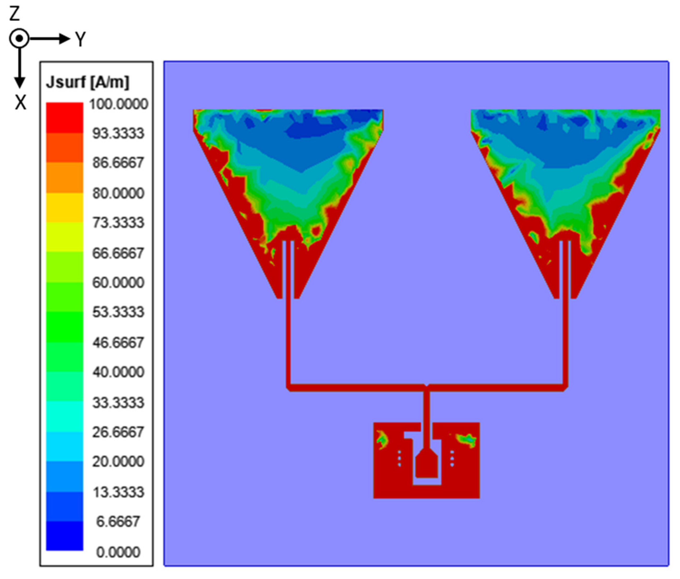
2.4. Surface Current Analysis
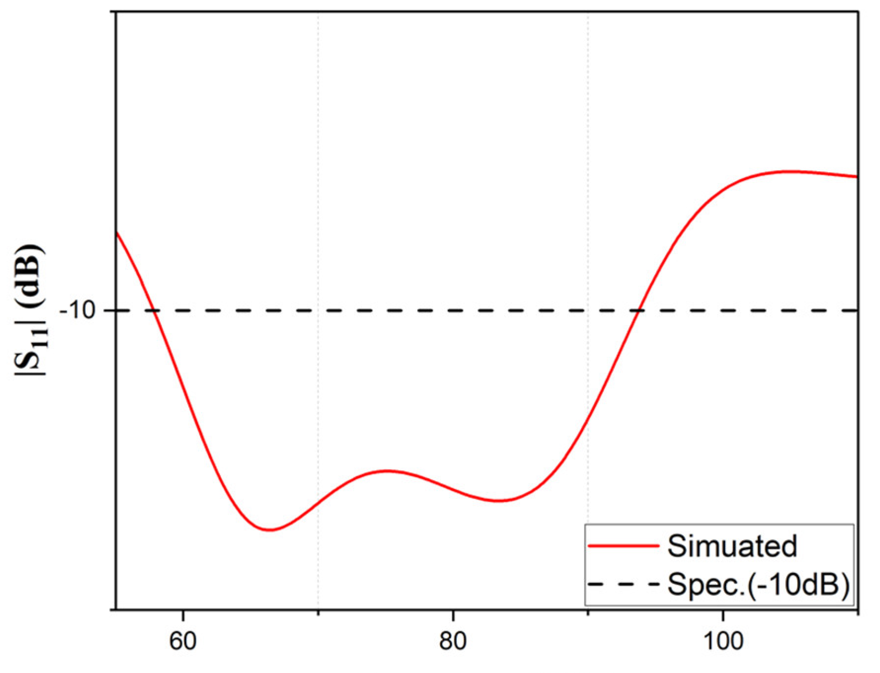
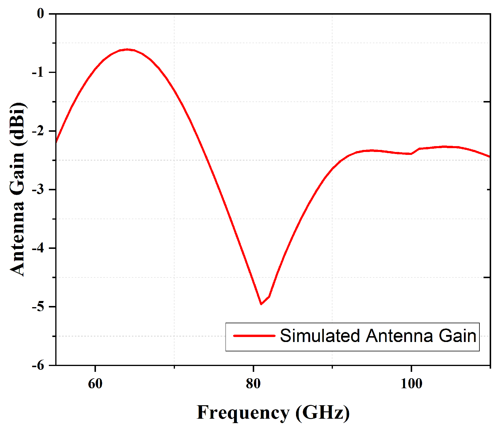
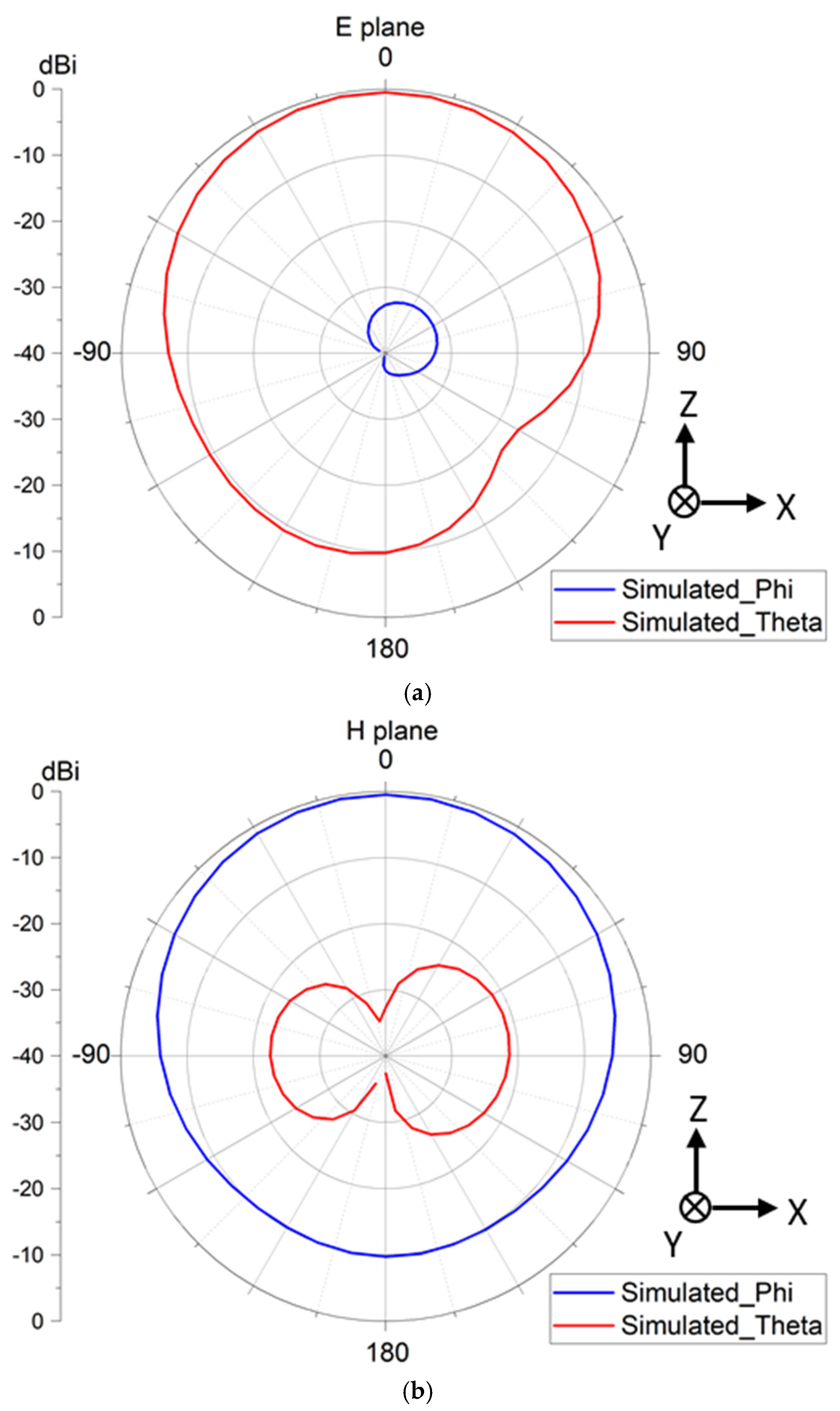
The Figure 13 shows the current distribution of the antenna at 64 GHz. The chip antenna proposed in this article uses a GSG probe to feed. The current flows evenly through the feed line and power divided into two triangular patch antennas. The current is mainly distributed on both sides of the power divider and triangular patch antenna. As can be seen from the figure, the current distribution of the power divider is average and consistent. After the triangular patch antenna is connected, the current is mainly distributed on both sides of the triangular patch antenna, making the antennas at both ends generate optimal resonance.

3. Results

In order to verify the design results, we measured the reflection coefficient of the antenna. Figure 14 shows the antenna measurement state diagram taken using a high magnification lens. The instrument for this measurement is shown in Figure 15. The Agilent E7350A vector network analyzer is used for measurement, with a measurement range of 2 GHz to 110 GHz. Using a GSG probe feed to measure the reflection coefficient, the probe spacing is 50 μm. As shown in Figure 16, the measured operating frequency is 62–100 GHz at the −10 dB reflection coefficient standard. The trend of simulation and measurement results is generally similar, but the measured results have a better reflection coefficient compared to the simulation, presumably due to the impedance matching effect when the probe is inserted.
Figure 17a,b illustrates chip antenna E plane and H plane views at 64 GHz. As shown in Figure 17a, at an operating frequency of 64 GHz, the E plane field type has a maximum gain of −0.4 dBi at a Theta of 0 deg. Figure 17b shows the radiation field pattern of the antenna in the H plane, with a maximum gain of −0.4 dBi when Phi is 0 deg. From the above results, it can be seen that the chip antenna proposed in this article radiates upward and has a good radiation field pattern.

4. Discussion

From the above parameter analysis, it can be seen that designing the feed line length of the patch antenna and the triangular patch antenna can help achieve a better reflection coefficient and frequency bandwidth percentage. Additionally, better impedance matching can be achieved by projecting a frog circular slot in both directions. Table 2 provides various parameters related to the chip antenna literature in recent years. The process, frequency, bandwidth, gain, efficiency, and size used in each document are listed in the table. Compared with the chip antenna design proposed in this article, it can be seen that the bandwidth is better than that of the references [18,19,20,21,22,23,24,25,26,27]. In terms of gain, it is better than references [18,20,22,23]. The efficiency is better than the literature [18,20,22,25]. The dimensions have advantages over references [19,20,21,26]. Based on the above, the chip antenna proposed in this paper is competitive in terms of bandwidth, gain, efficiency, and size. The antenna proposed in this paper has good bandwidth and radiation performance and is suitable for application in millimeter wave systems.

5. Conclusions

Chip antennas are a good candidate for millimeter wave system applications that require high integration and broadband characteristics. This paper proposes a chip antenna suitable for millimeter wave systems using 0.18 μm CMOS process, which size is 1.2 × 1.2 (mm2), using an M6 metal layer for antenna design. Through parameter analysis, it can be seen that the optimization of the feed line length and patch shape is helpful for antenna impedance matching. In addition, by expanding to a 1 × 2 array antenna pole and digging three circular slots in the ground, antenna radiation performance is increased. The proposed chip antenna in this paper has a gain of −0.4 dBi at 64 GHz, maximum. The proposed antenna has a fractional bandwidth 54%. The actual measured bandwidth is 62–100 GHz, and the analog and measured bandwidth are similar. The chip antenna frequency range proposed in this article covers the 5G NR FR2 frequency band and can be used in the fields of the Internet of Things, Industry 4.0, and biomedical electronics. Its small size makes it easy to integrate with other microwave circuits, which can form a highly integrated millimeter wave system. In the future, it will be able to integrate with microwave circuits or combine applications with printed circuit boards to further improve antenna gain performance.

Author Contributions

Conceptualization, M.-A.C.; methodology, M.-A.C.; software, M.-A.C. and S.-R.H.; validation, M.-A.C., S.-R.H. and P.-R.H.; formal analysis, M.-A.C., S.-R.H. and P.-R.H.; investigation, M.-A.C., S.-R.H. and P.-R.H.; resources, M.-A.C.; writing—original draft preparation, M.-A.C. and S.-R.H.; writing—review and editing, M.-A.C.; visualization, M.-A.C.; supervision, M.-A.C.; project administration, M.-A.C.; funding acquisition, M.-A.C. All authors have read and agreed to the published version of the manuscript.

Funding

This research received no external funding.

Data Availability Statement

All data are included within the manuscript.

Acknowledgments

Not applicable.

Conflicts of Interest

The authors declare no conflict of interest.

References

  1. Wang, Y.; Wu, R.; Pang, J.; You, D.; Fadila, A.A.; Saengchan, R.; Fu, X.; Matsumoto, D.; Nakamura, T.; Kubozoe, R. A 39-GHz 64-element phased-array transceiver with built-in phase and amplitude calibrations for large-array 5G NR in 65-nm CMOS. IEEE J. Solid-State Circuits 2020, 55, 1249–1269. [Google Scholar] [CrossRef]
  2. Haseeb, K.; Saba, T.; Rehman, A.; Ahmed, Z.; Song, H.H.; Wang, H.H. Trust management with fault-tolerant supervised routing for smart cities using internet of things. IEEE Internet Things J. 2022, 9, 22608–22617. [Google Scholar] [CrossRef]
  3. Jamshed, M.A.; Ali, K.; Abbasi, Q.H.; Imran, M.A.; Ur-Rehman, M. Challenges, applications and future of wireless sensors in Internet of Things: A review. IEEE Sens. J. 2022, 22, 5482–5494. [Google Scholar] [CrossRef]
  4. Zhu, P.; Yoshida, Y.; Kanno, A.; Kitayama, K.-I. DSP-enhanced radio-over-fiber technologies for 5G-and-beyond wired-wireless convergence. J. Opt. Commun. Netw. 2022, 14, 595–605. [Google Scholar] [CrossRef]
  5. Guo, Q.; Tang, F.; Kato, N. Federated Reinforcement Learning-Based Resource Allocation in D2D-Enabled 6G. IEEE Netw. 2022, 1–7. [Google Scholar] [CrossRef]
  6. Ndip, I.; Andersson, K.; Kosmider, S.; Le, T.H.; Kanitkar, A.; van Dijk, M.; Murugesan, K.S.; Maaß, U.; Löher, T.; Rossi, M. A novel packaging and system-integration platform with integrated antennas for scalable, low-cost and high-performance 5G mmWave systems. In Proceedings of the 2020 IEEE 70th Electronic Components and Technology Conference (ECTC), Orlando, FL, USA, 3–30 June 2020; pp. 101–107. [Google Scholar]
  7. De Kok, M.; Smolders, A.B.; Johannsen, U. A review of design and integration technologies for D-band antennas. IEEE Open J. Antennas Propag. 2021, 2, 746–758. [Google Scholar] [CrossRef]
  8. Alibakhshikenari, M.; Virdee, B.S.; Khalily, M.; See, C.H.; Abd-Alhameed, R.; Falcone, F.; Denidni, T.A.; Limiti, E. High-gain on-chip antenna design on silicon layer with aperture excitation for terahertz applications. IEEE Antennas Wirel. Propag. Lett. 2020, 19, 1576–1580. [Google Scholar] [CrossRef]
  9. Kong, S.; Shum, K.M.; Yang, C.; Gao, L.; Chan, C.H. Wide impedance-bandwidth and gain-bandwidth terahertz on-chip antenna with chip-integrated dielectric resonator. IEEE Trans. Antennas Propag. 2021, 69, 4269–4278. [Google Scholar] [CrossRef]
  10. Cheema, H.M.; Shamim, A. The last barrier: On-chip antennas. IEEE Microw. Mag. 2013, 14, 79–91. [Google Scholar] [CrossRef]
  11. Deng, X.-D.; Li, Y.; Liu, C.; Wu, W.; Xiong, Y.-Z. 340 GHz on-chip 3-D antenna with 10 dBi gain and 80% radiation efficiency. IEEE Trans. Terahertz Sci. Technol. 2015, 5, 619–627. [Google Scholar] [CrossRef]
  12. Van Berkel, S.; Malotaux, E.S.; De Martino, C.; Spirito, M.; Cavallo, D.; Neto, A.; Llombart, N. Wideband double leaky slot lens antennas in CMOS technology at submillimeter wavelengths. IEEE Trans. Terahertz Sci. Technol. 2020, 10, 540–553. [Google Scholar] [CrossRef]
  13. Chung, M.-A.; Chen, Y.-H.; Meiy, I.-P. Antenna-on-Chip for Millimeter Wave Applications Using CMOS Process Technology. Telecom 2023, 4, 146–164. [Google Scholar] [CrossRef]
  14. Khan, W.T.; Ulusoy, A.Ç.; Dufour, G.; Kaynak, M.; Tillack, B.; Cressler, J.D.; Papapolymerou, J. A D-band micromachined end-fire antenna in 130-nm SiGe BiCMOS technology. IEEE Trans. Antennas Propag. 2015, 63, 2449–2459. [Google Scholar] [CrossRef]
  15. Yuan, S.; Trasser, A.; Schumacher, H. 56 GHz bandwidth FMCW radar sensor with on-chip antennas in SiGe BiCMOS. In Proceedings of the 2014 IEEE MTT-S International Microwave Symposium (IMS2014), Tampa, FL, USA, 1–6 June 2014; pp. 1–4. [Google Scholar]
  16. Lee, C.; Jeong, J. THz cmos on-chip antenna array using defected ground structure. Electronics 2020, 9, 1137. [Google Scholar] [CrossRef]
  17. Ciccia, S.; Giordanengo, G.; Vecchi, G. Energy efficiency in IoT networks: Integration of reconfigurable antennas in ultra low-power radio platforms based on system-on-chip. IEEE Internet Things J. 2019, 6, 6800–6810. [Google Scholar] [CrossRef]
  18. Burasa, P.; Djerafi, T.; Wu, K. A 28 GHz and 60 GHz dual-band on-chip antenna for 5G-compatible IoT-served sensors in standard CMOS process. IEEE Trans. Antennas Propag. 2020, 69, 2940–2945. [Google Scholar] [CrossRef]
  19. Mustacchio, C.; Boccia, L.; Arnieri, E.; Amendola, G. A gain levelling technique for on-chip antennas based on split-ring resonators. IEEE Access 2021, 9, 90750–90756. [Google Scholar] [CrossRef]
  20. Burasa, P.; Djerafi, T.; Constantin, N.G.; Wu, K. On-chip dual-band rectangular slot antenna for single-chip millimeter-wave identification tag in standard CMOS technology. IEEE Trans. Antennas Propag. 2017, 65, 3858–3868. [Google Scholar] [CrossRef]
  21. Sultan, K.S.; Abdallah, E.A.; El Hennawy, H. A multiple-input-multiple-output on-chip Quasi-Yagi-Uda antenna for multigigabit communications: Preliminary study. Eng. Rep. 2020, 2, e12133. [Google Scholar] [CrossRef]
  22. Liu, Q.; van den Biggelaar, A.; Johannsen, U.; van Beurden, M.C.; Smolders, A.B. On-chip metal tiling for improving grounded mm-Wave antenna-on-chip performance in standard low-cost packaging. IEEE Trans. Antennas Propag. 2019, 68, 2638–2645. [Google Scholar] [CrossRef]
  23. Khan, M.S.; Tahir, F.A.; Meredov, A.; Shamim, A.; Cheema, H.M. A W-band EBG-backed double-rhomboid bowtie-slot on-chip antenna. IEEE Antennas Wirel. Propag. Lett. 2019, 18, 1046–1050. [Google Scholar] [CrossRef]
  24. Van den Brande, Q.; Lemey, S.; Cuyvers, S.; Poelman, S.; De Brabander, L.; Caytan, O.; Bogaert, L.; De Paula, I.L.; Verstuyft, S.; Reniers, A.C. A hybrid integration strategy for compact, broadband, and highly efficient millimeter-wave on-chip antennas. IEEE Antennas Wirel. Propag. Lett. 2019, 18, 2424–2428. [Google Scholar] [CrossRef]
  25. Hedayati, M.K.; Abdipour, A.; Shirazi, R.S.; Ammann, M.J.; John, M.; Cetintepe, C.; Staszewski, R.B. Challenges in on-chip antenna design and integration with RF receiver front-end circuitry in nanoscale CMOS for 5G communication systems. IEEE Access 2019, 7, 43190–43204. [Google Scholar] [CrossRef]
  26. Song, Y.; Xu, Q.; Tian, Y.; Yang, J.; Wu, Y.; Tang, X.; Kang, K. An on-chip frequency-reconfigurable antenna for Q-band broadband applications. IEEE Antennas Wirel. Propag. Lett. 2017, 16, 2232–2235. [Google Scholar] [CrossRef]
  27. Wu, L.; Huang, J.; Sun, B.; Chang, H.; Huang, S.; Liu, H. Miniaturized broadband monopole antenna in 130nm CMOS with gain improvement. IEICE Electron. Express 2022, 19, 20220076. [Google Scholar] [CrossRef]
Figure 1. The top view of proposed chip antenna.
Inventions 08 00064 g001
Figure 2. The antenna stack architecture of proposed chip antenna.
Inventions 08 00064 g002
Figure 3. Proposed chip antenna geometry.
Inventions 08 00064 g003
Figure 4. Simulated S11 of the antenna.
Inventions 08 00064 g004
Figure 5. Simulated antenna gain.
Inventions 08 00064 g005
Figure 6. Simulated antenna efficiency.
Inventions 08 00064 g006
Figure 7. Antenna parameter L3 evolution diagram.
Inventions 08 00064 g007
Figure 8. Reflection coefficient of antenna feed line variation.
Inventions 08 00064 g008
Figure 9. Triangular patch evolution diagram.
Inventions 08 00064 g009
Figure 10. Reflection coefficient of W2 variation.
Inventions 08 00064 g010
Figure 11. Diagram of different numbers of circular slot.
Inventions 08 00064 g011
Figure 12. Reflection coefficient of different numbers of circular slot.
Inventions 08 00064 g012
Figure 13. An amount of 64 GHz surface current of chip antenna.
Inventions 08 00064 g013
Figure 14. GSG connector and actual measurement diagram.
Inventions 08 00064 g014
Figure 15. Measurement environment setup.
Inventions 08 00064 g015
Figure 16. Reflection coefficient of simulation and measurement of chip antenna.
Inventions 08 00064 g016
Figure 17. 2D Radiation Pattern (a) E Plane; (b) H Plane.
Inventions 08 00064 g017
Table 1. Parameters of the proposed chip antenna.
ParameterValue (μm)ParameterValue (μm)
W1200L1200
W1450L150
W2200L2400
W310L3350
W412L415
W5110L520
W640L620
W720L7140
W810L875
W950L945
W1070L1090
W11250L1120
Table 2. Comparison table with the other research literature.
ReferenceProcess* Freq. (GHz)* FBW (%)Gain (dBi)* Eff. (%)Size (mm2)
This Work0.18 μm CMOS6454−0.440.91.2 × 1.2
[18]0.65 μm CMOS28, 605.3, 5.9−10, 445, 300.25 × 0.3
[19]0.13 μm SiGe CMOS81.512.11.61NA1.296 × 1.508
[20]0.65 μm CMOS24, 4019, 20−1, 041, 312.5 × 2.5 × 2.5
[21]0.18 μm CMOS60160.3455 × 5
[22]CMOS609.8−2.3211.5 × 0.75
[23]0.13 μm BiCMOS8411.7−0.5410.32 × 0.1
[24]MEMS28.5136.690.90.52 × 0.52
[25]0.28 μm CMOS3316.31437.30.66 × 0.85
[26]0.18 μm CMOS4053.43.3NA1.1 × 1.7
[27]0.13 μm CMOS8131.4−0.3NA0.1 × 0.05
* Freq.: Frequency; * FBW: Fractional bandwidth; * Eff: Efficiency.
Disclaimer/Publisher’s Note: The statements, opinions and data contained in all publications are solely those of the individual author(s) and contributor(s) and not of MDPI and/or the editor(s). MDPI and/or the editor(s) disclaim responsibility for any injury to people or property resulting from any ideas, methods, instructions or products referred to in the content.

