1. Introduction
The increasing demand for wireless connections has led to data traffic congestion on the traditional microwave spectrum. To cope with such huge demand, the Third Generation Partner Program (3GPP) expanded the frequency band of 5G new radio (5G NR) to FR1 (0.4 GHz–7.1 GHz) and FR2 (24.2 GHz–52.6 GHz) to achieve higher connectivity, a higher data rate, ultra-low latency, higher energy efficiency, and higher spectral efficiency to process these data and information [
1,
2]. Under the network coverage of the fifth-generation mobile communication, billions of physical devices worldwide are connected to the Internet and transmit a large amount of data information through a network independent of human behavior [
3,
4]. The Internet of Things has promoted the rapid growth of smart homes, smart cities, smart grids, industrial automation, health care, environment, and traffic monitoring. Even the sudden outbreak of the coronavirus epidemic did not show a downward trend in demand [
5,
6,
7]. With the transformation of mobile communication networks, there is more and more research on the frequency bands of millimeter wave communication systems, including n257 (26.5 GHz–29.5 GHz), n258 (24.2 GHz–27.5 GHz), n259 (39.5 GHz–43.5 GHz), n260 (37 GHz–40 GHz), and n261 (27.5 GHz–28.3 GHz). The realization of high-performance, low-cost and low-power transceivers has become an important research topic [
8]. At the same time, the 60 GHz and 77 GHz bands are also being studied in the fields of industry, science, medical treatment, and automotive radar [
9]. In addition to the millimeter wave band, the terahertz above 100 GHz is also attracting attention. Technological progress has meant that the development of terahertz is also included in the possibility of future mobile networks [
10]. The terahertz can be applied to physical systems such as autonomous driving vehicles, robot networks, and virtual reality or in intelligent sensing, imaging, defect detection, short-range wireless communication, and other applications [
11].
In the past two decades, integrated circuits have made a breakthrough in growth because of advanced technology. Billions of transistors can be manufactured on a few square millimeters of a wafer, and the precision of manufacturing technology is becoming more and more mature [
12]. As the high-frequency capability of chip antenna is improved through scaling, the complementary metal oxide semiconductor (CMOS) has become a feasible manufacturing method for chip antenna and can integrate a complete chip antenna system on a single chip through CMOS technology, further improving the competitiveness of the system [
13,
14]. Compared with the traditional antenna system, the chip antenna system has higher bandwidth, better integration, and lower power consumption. In addition, as the most critical part of the system, the chip antenna eliminates the parasitic effect and uncertainty of the circuit caused by additional connections. The chip antenna can be directly connected to the circuit without an additional matching network, which provides more flexible design methods for designers and facilitates chip layout [
15,
16]. In addition to the millimeter wave spectrum, CMOS technology is also considered a good choice for the terahertz because its scaling and low-cost technology also have characteristics of high-density integration and performance improvement like the millimeter wave system. For this reason, the chip antenna in the terahertz is also crucial to the terahertz system [
17]. The progress of communication technology has brought great potential for the development of terahertz, which will be applied in medical imaging, astronomy, and other fields in the future [
18].
In recent years, millimeter wave chips have been extensively studied. They have different orientations and implementation methods, such as miniaturization [
19], resonance analysis [
20,
21], integrated circuit design [
22,
23], the introduction of AMCs [
24,
25,
26], and integration with printed circuit boards [
8,
27]. In [
19], based on the 130 nm CMOS process, a miniaturized broadband monopole antenna for the W-band was proposed. This paper reduces the size by 16.2% by using the hexagonal grid structure, and analyzes the angle of the grid to optimize impedance matching. For the bandwidth, the capacitance effect of the sixth and first layers of metal is used to achieve broadband, and the antenna bandwidth is 31.5%. In [
20], it could improve the gain of 7 dBi at 85 GHz, and the maximum gain measured at 81.5 GHz is 1.61 dBi by coupling with the feed antenna by adding a square resonant ring. Ref. [
21] analyzed the influence of the number of twists of the monopole antenna on the operating frequency. According to the simulation results, there was resonance at 28 GHz and 60 GHz, achieving the purpose of dual frequency. In addition, considering the chip layout, the packaging substrate was selected and placed under the silicon substrate to radiate coherently and constructively at two frequencies, to enhance the antenna gain and efficiency. In [
22], the voltage-controlled oscillator and frequency multiplier were used as the back-end circuit to improve the gain of 7 dBi. In [
23], a switching circuit was introduced, and the total bandwidth was increased to 53.4% under two working conditions. In [
24], the thickness of the AMC was reduced through two methods, namely, the metal post and an embedded guiding structure, and the gain at 94 GHz was 5.8 dBi, which was 9.1 dBi higher than that without the AMC. In [
25], the parasitic capacitance generated by the double-layer AMC regulated the impedance and bandwidth. It was confirmed that the bandwidth increased to 5.8 GHz, and an input impedance consistent with the measurement was obtained. In [
26], different AMC elements were analyzed and compared. The results showed that the back-to-back E-shaped (B2BE) framework proposed in this paper had the best bandwidth (75 GHz–125 GHz) and reflection coefficient, and it was applied to the antenna. In [
27], efficiency improved by more than 90% through the air-filled substrate synthesis waveguide technology. In [
8], the slot and antenna on the PCB board were embedded and integrated into the back-end circuit, which improved the total gain of 21.6 dBi.
In this paper, a small-size broadband slot monopole chip antenna is proposed, using the 0.18 μm CMOS manufacturing process, with an antenna sized 1.2 × 1.2 (mm2). The Metal_1 layer is used as an AMC to improve the impedance matching of the antenna. The proposed design of the slot and external branch improves the bandwidth performance. The measurement results show that the bandwidth is 33.8 GHz–110 GHz, and the fractional bandwidth is 103.4% under the spec. of reflection coefficient of −10 dB. At 72 GHz, the maximum gain is −6.3 dBi. The frequency covers 5G NR FR2 (24.2 GHz–52.6 GHz) and W-band (75 GHz–110 GHz). The proposed chip antenna is small and easy to integrate with a millimeter wave system and can be used in near-field sensing applications. The rest of this paper organized as follows: The second chapter describes the geometry, simulation result, parameter analysis, and current distribution of the proposed chip antenna. The third chapter compares measurement and simulation results and explains the differences between measurement and simulation. The fourth chapter describes the performance compared with recent literature and points out the advantages of the proposed chip antenna. Finally, the performance and characteristics of this antenna are summarized in chapter five.
2. Materials and Methods
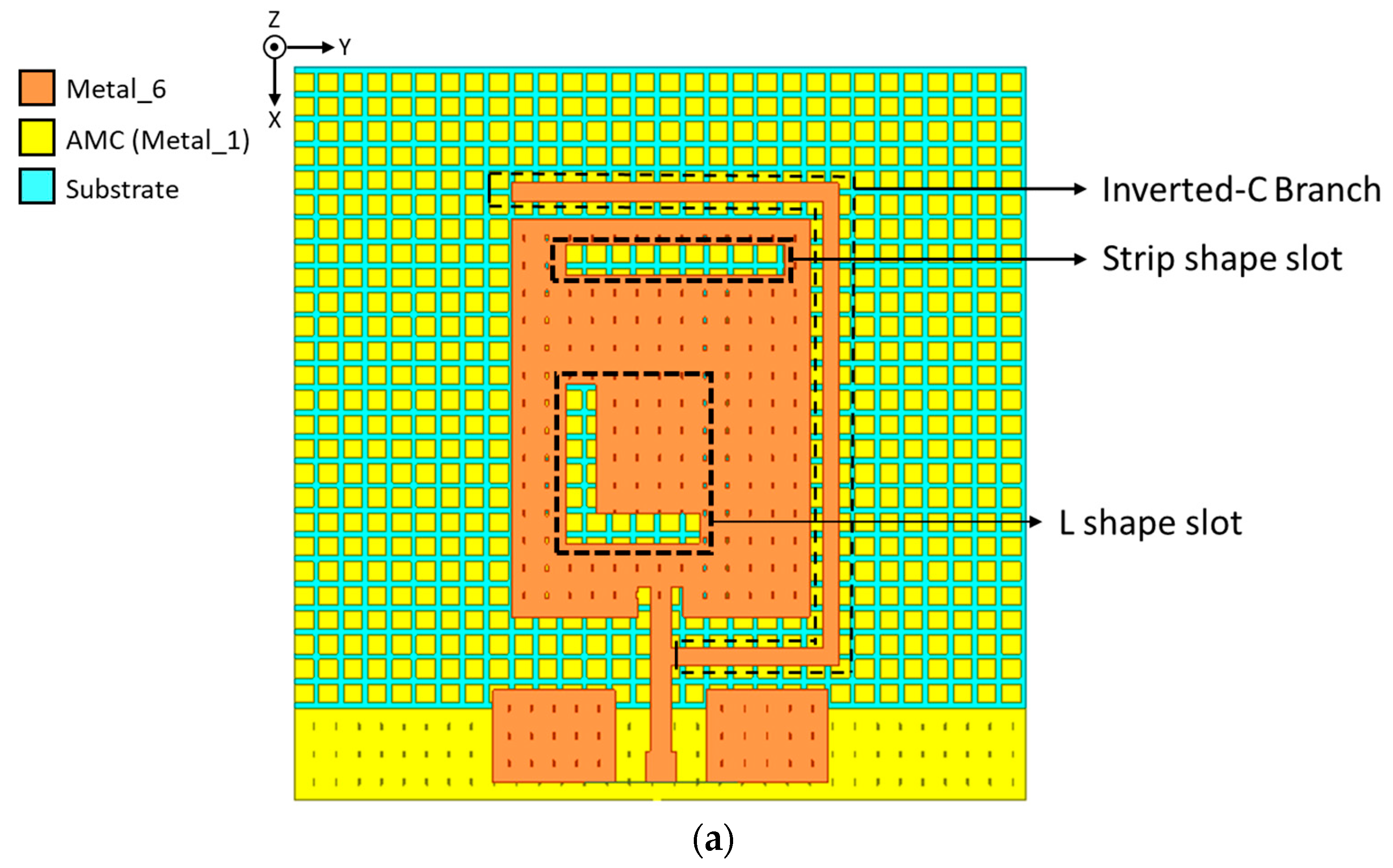
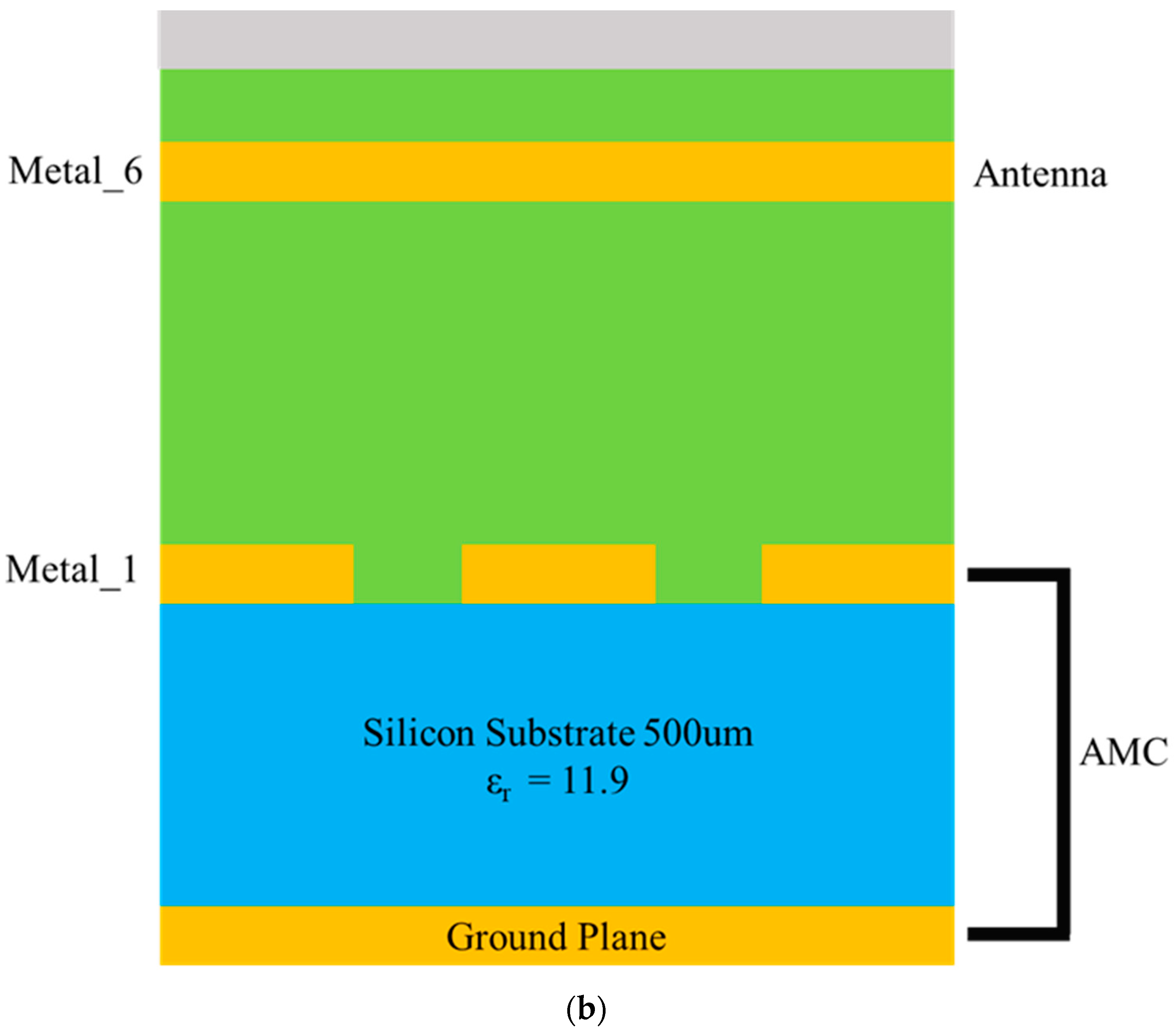
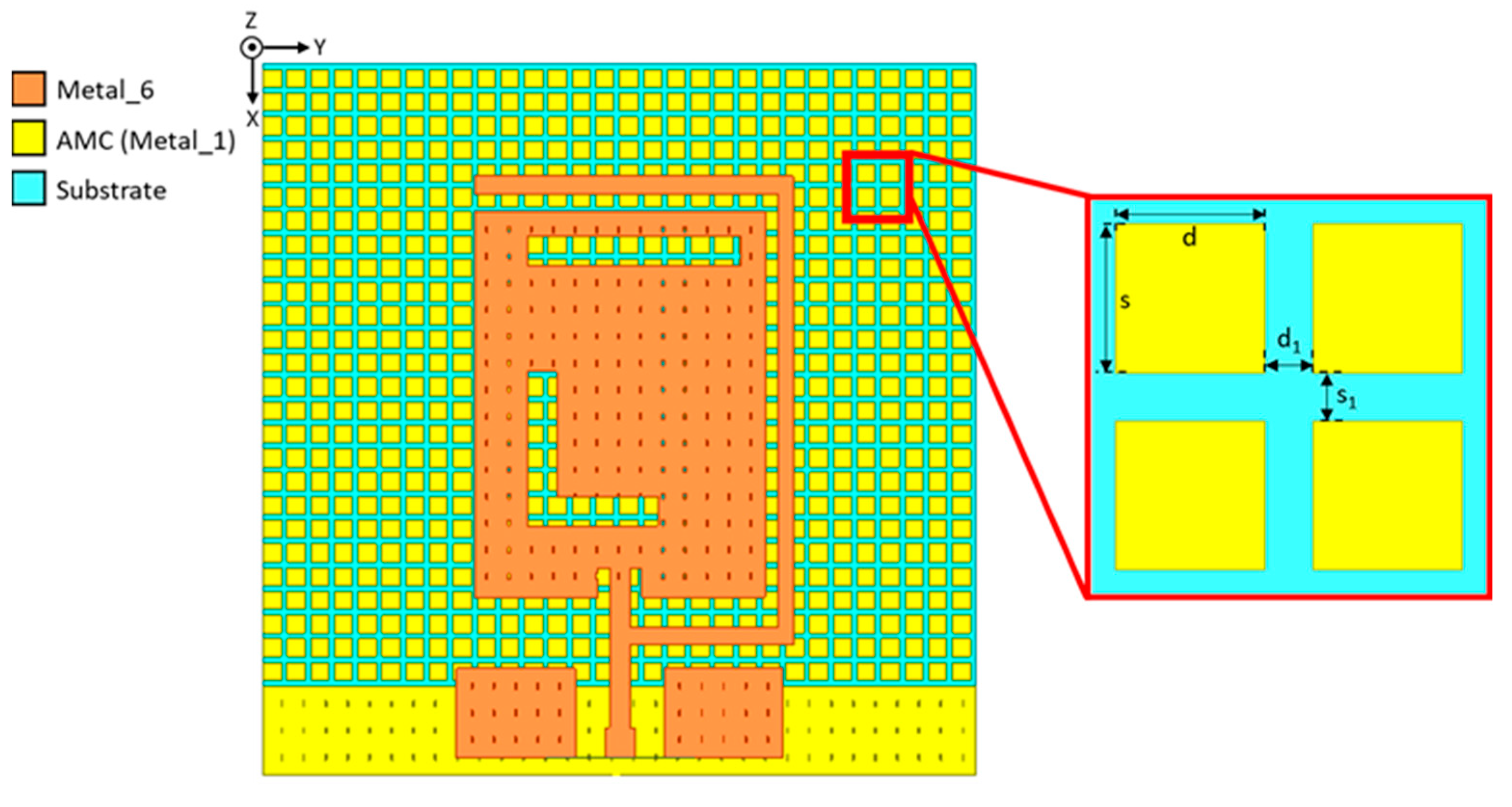
Figure 1 shows the chip antenna proposed in this paper by using an 0.18 μm CMOS process design and GSG feed structure.
Figure 1a is the top view of the proposed chip antenna. The chip antenna is composed of a patch as the main body, a strip slot and an L-shaped slot are dug on the patch antenna, and an inverted C branch is added to form the antenna body. In addition, the chip stacking structure is shown in
Figure 1b. The Metal_6 layer is used as an antenna, and the square patch is introduced in the Metal_1 layer to form an AMC structure with the ground plane, reducing the high dielectric loss caused by the silicon substrate.
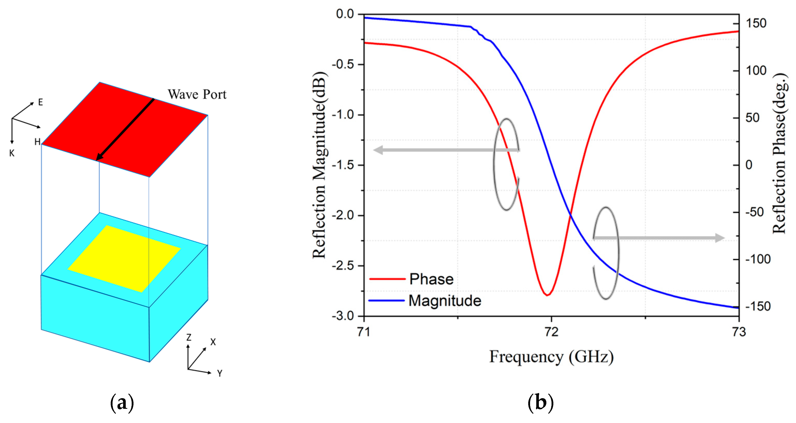
This paper also simulated and analyzed the AMC unit’s reflection coefficient and phase.
Figure 2a is the structure diagram of the AMC unit model. To get close to the actual situation, the PEC boundary was used in the XZ plane, the PMC boundary was used in the YZ plane, and the wave port was used in the +Z direction of 1/4 wavelength from the AMC. The reflection coefficient and phase simulation results of AMC are shown in
Figure 2b. In the 72GHz operating frequency band, it had phase bandwidth and a high reflection coefficient.
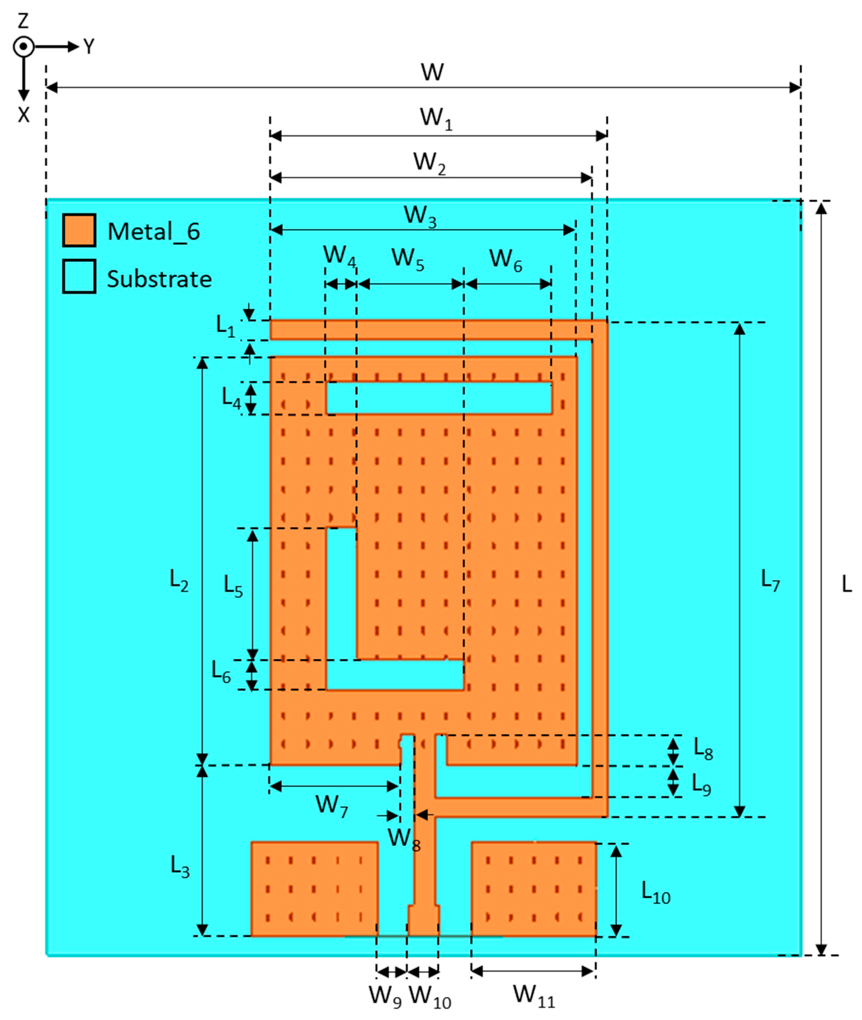
Figure 3 shows the proposed chip antenna geometry and the value of dimensions shown in
Table 1. The detailed geometric dimensions of the strip slot, L-slot, and inverted C-branch are clearly indicated in the table. The geometric size of the AMC unit is shown in
Figure 4 and
Table 2. According to the literature [
28], the square patch was selected in this paper due to its larger bandwidth and lower loss.
Figure 5,
Figure 6 and
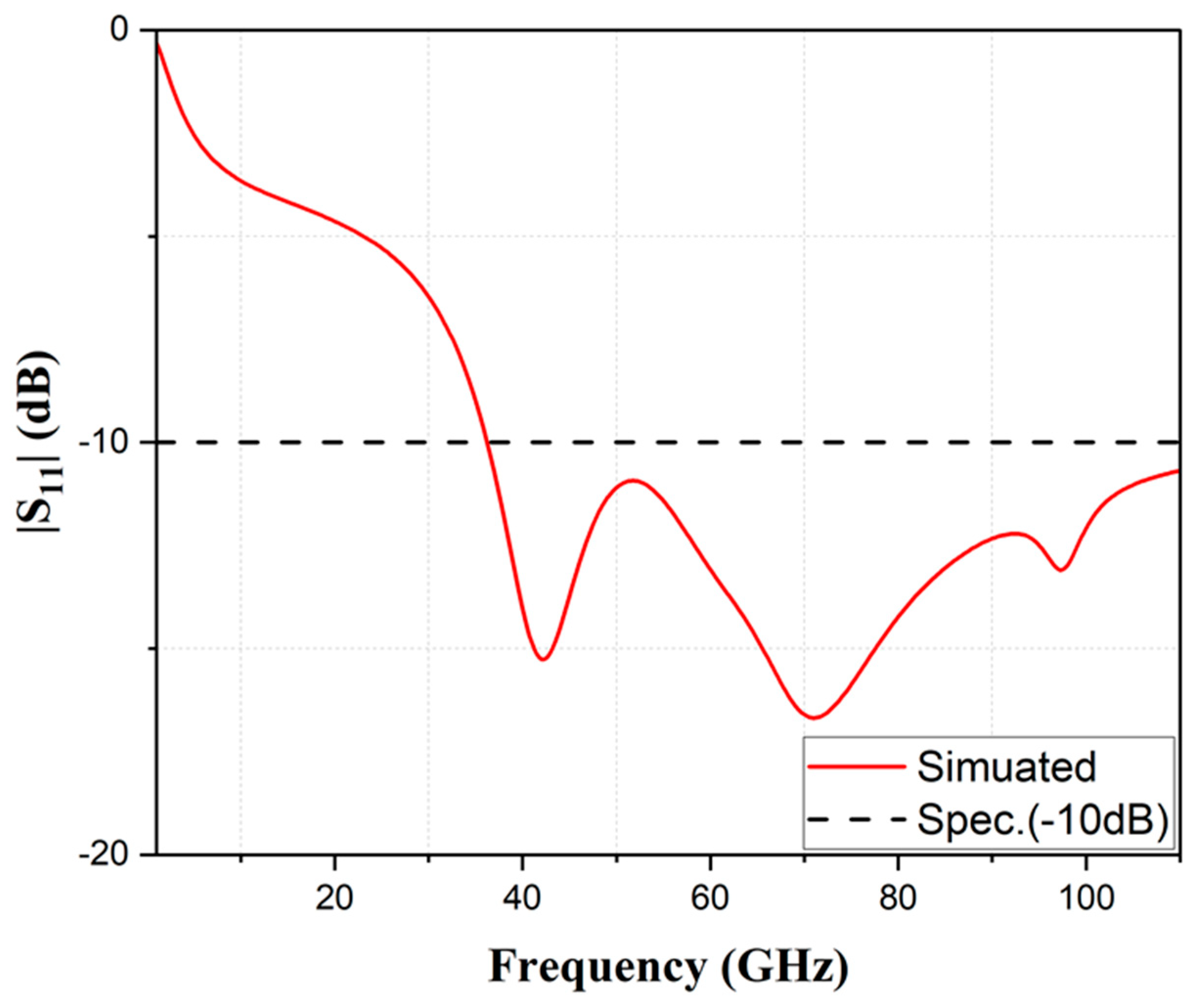
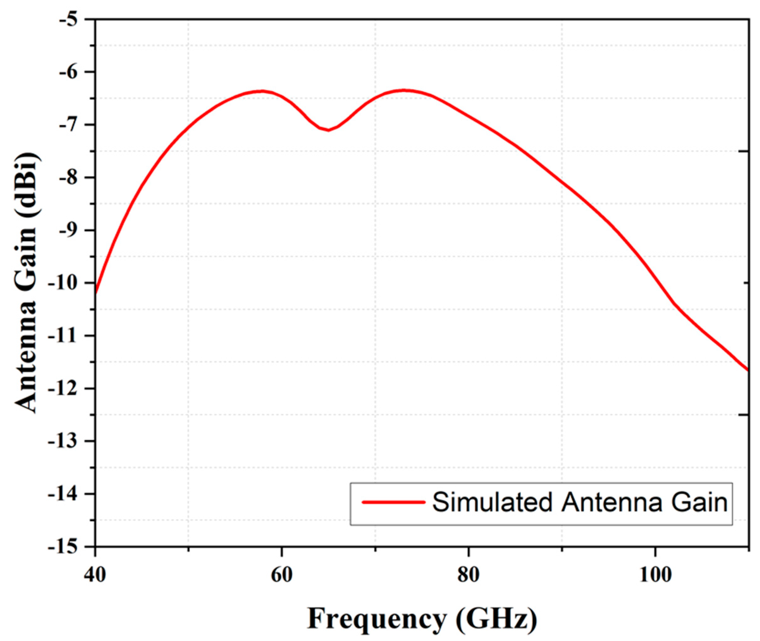
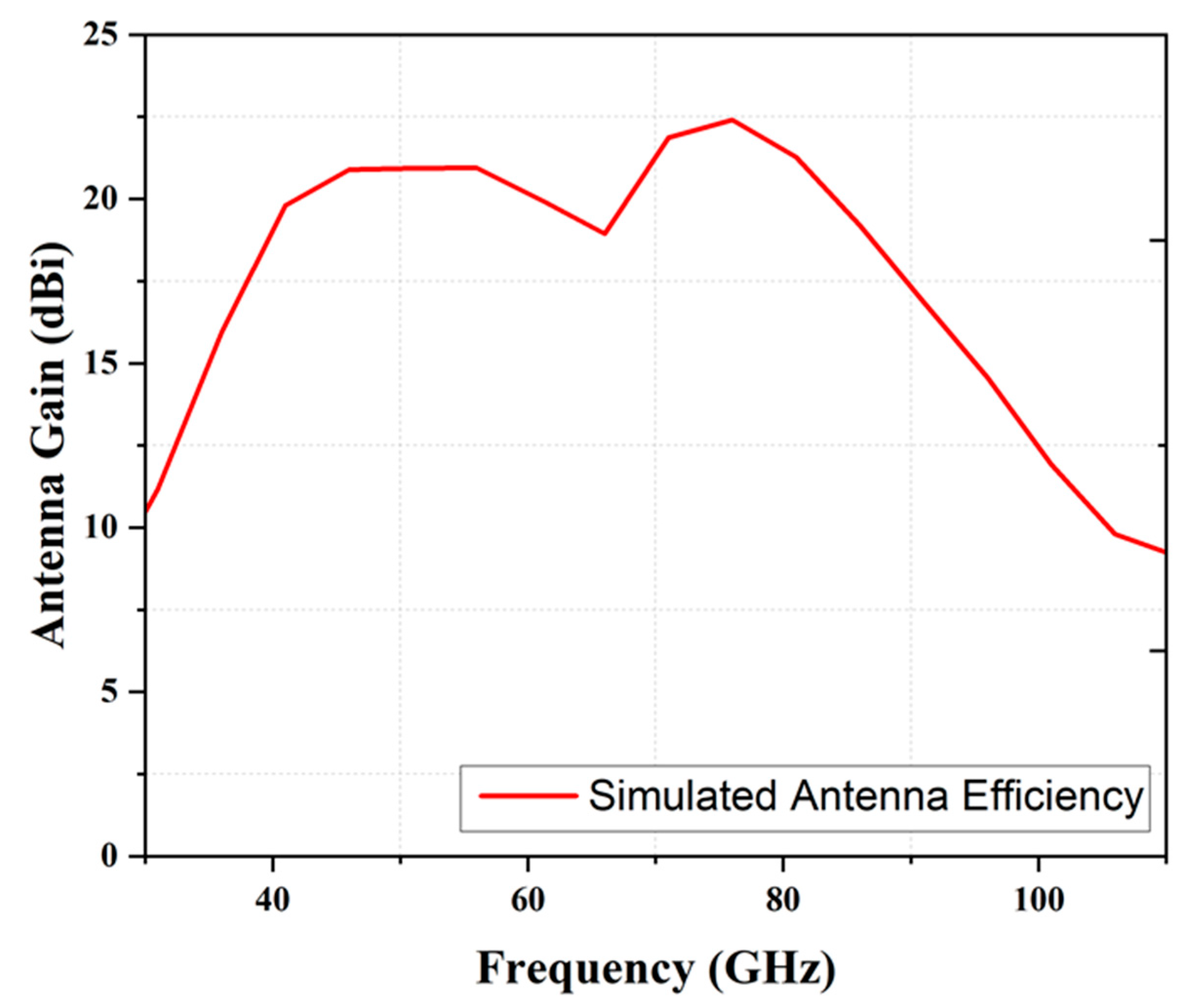
Figure 7 show the simulation results of the reflection coefficient, gain, and efficiency of the proposed antenna. Simulation analysis was performed through high-frequency electromagnetic simulation software. In
Figure 5, when the reflection coefficient was less than −10 dB, the antenna bandwidth was 34.8 GHz–110 GHz and there were resonance points at 42 GHz, 72 GHz, and 96 GHz. The simulation results show that there were broadband characteristics. It can be seen from
Figure 6 and
Figure 7 that there was a peak gain of −6.3 dBi and a maximum efficiency of 22% at 72 GHz.
2.1. Parameter Analysis of Antenna Slot
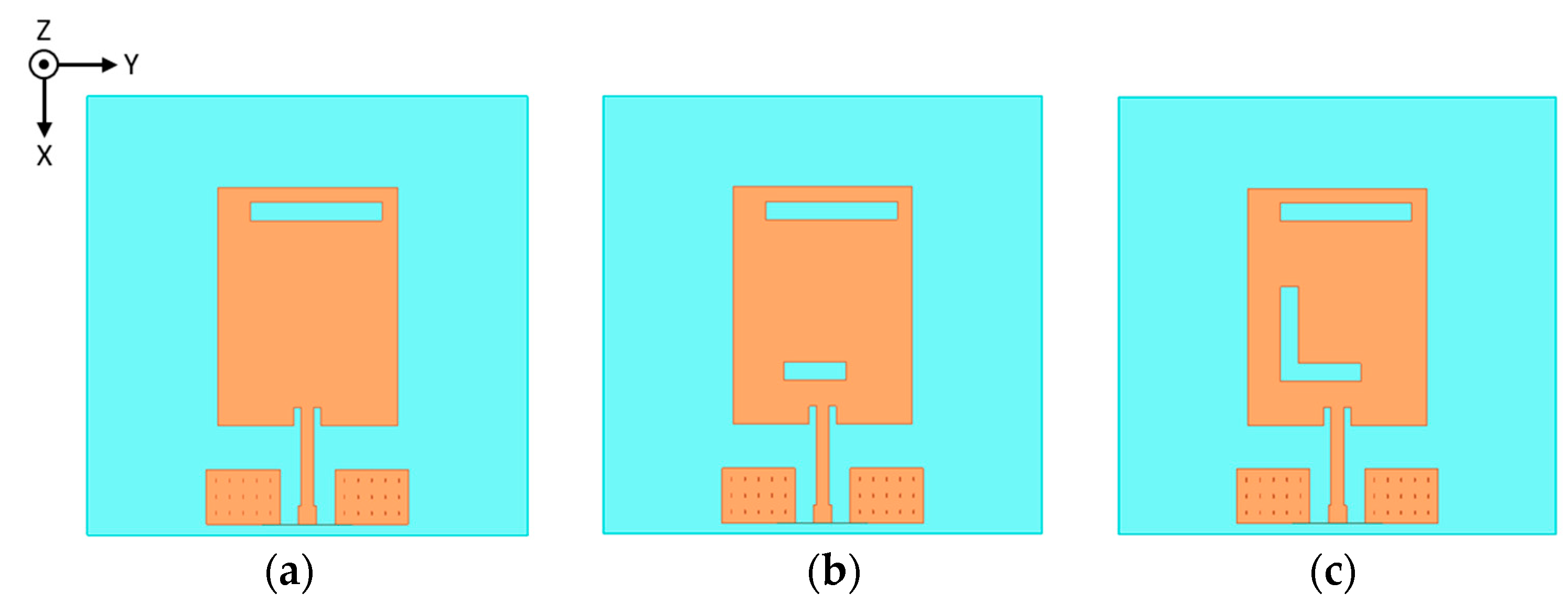
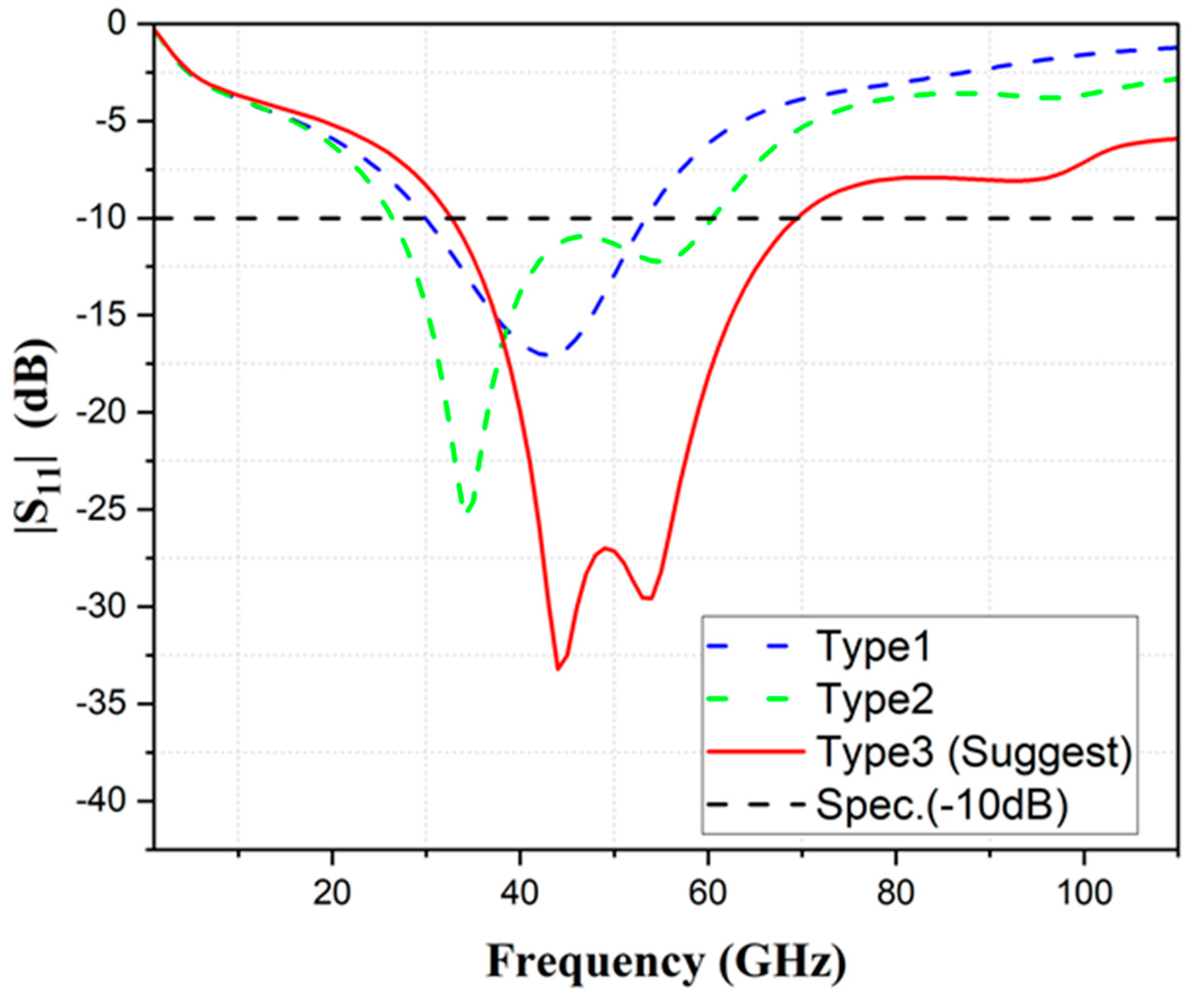
In this paper, we only simulated and analyzed the antenna slot structure, observed the effect of the slot on the antenna, and took the reflection coefficient of less than −10 dB as the standard. The gap evolution was divided into three parts. First, the feed end was measured with the GSG structure, and the distance between PADs was W9 = 50 μm. The evolution diagram and simulation results of the antenna slot structure are shown in
Figure 8a–c and
Figure 9.
Figure 8a has only one slot. The bandwidth of this type was 30 GHz–53 GHz, and there was a −17 dB resonance at 43 GHz. In addition to the strip gap,
Figure 8b dug another strip gap near the feeder line to obtain a bandwidth of 26.3 GHz–60.4 GHz. There was resonance at 34 GHz and 55 GHz, respectively: −25.3 dB and −12.2 dB. Compared with
Figure 8a,
Figure 8b had 11.1 GHz more bandwidth. For
Figure 8c, we formed an L-shaped gap with the strip gap close to the feeder line by digging the strip gap. At this time, the bandwidth was 32.6 GHz–69.4 GHz. There was resonance at 44 GHz and 55 GHz, with individual values of −33.2 dB and −28.1 dB. Compared with
Figure 8b, the bandwidth was 2.7 GHz more. It can be seen from the above results that the bandwidth of the antenna increased gradually after increasing the strip slot and L-slot. In
Figure 8c, the overall bandwidth was 36.2 GHz, with the best operating frequency band.
2.2. Parameter Analysis of Antenna Branches
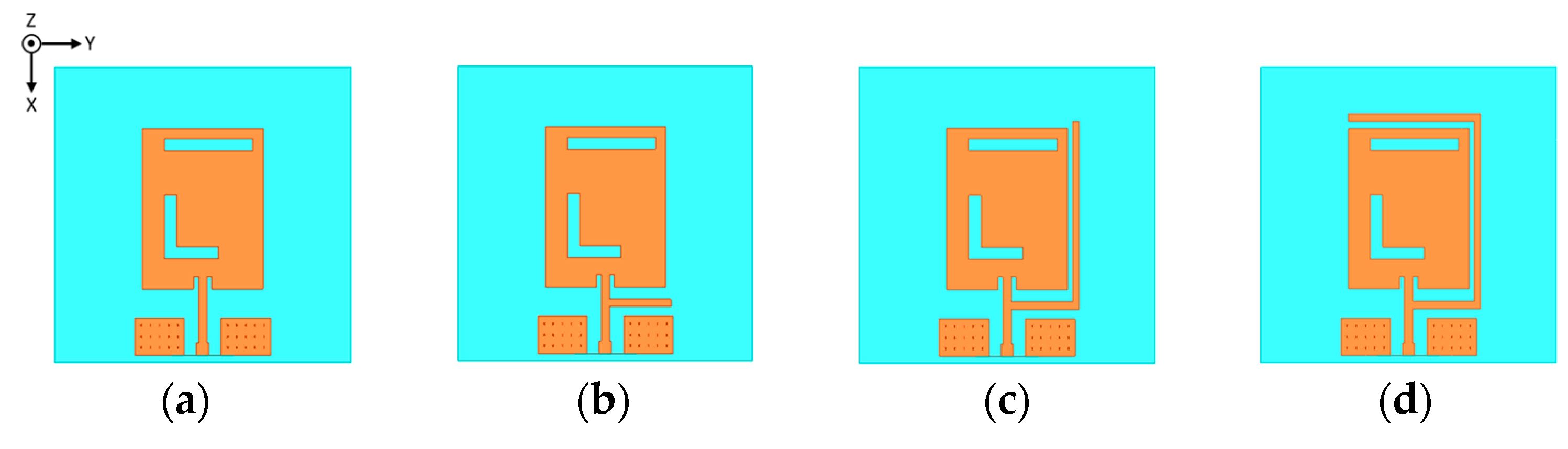
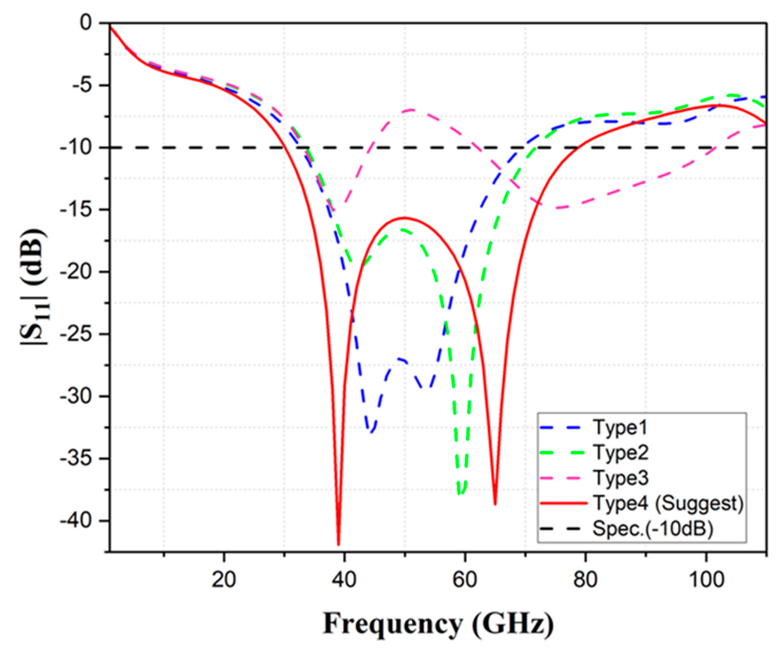
Then, we conducted a simulation analysis for the inverted C branch of the antenna, which was divided into four types. The evolution diagram of the antenna branch structure and the simulation results are shown in
Figure 10a–d and
Figure 11. The reflection coefficient was also less than −10 dB, as the parameter standard. In
Figure 10a, when no branch was added, the bandwidth of this type was 32.6 GHz–69.4 GHz. Moreover, there was resonance at 44 GHz and 54 GHz, which were −33.2 dB and −28.1 dB, respectively.
Figure 10b added a single transverse branch beside the feeder line. The frequency width was 33.5 GHz–71.6 GHz, and there was resonance at 42 GHz and 59 GHz. The individual values were −19.6 dB and −38.3 dB. Compared with
Figure 10a, the frequency width was 1.3 GHz more.
Figure 10c added a straight line branch to the horizontal branch, which could obtain 33.2 GHz–44.4 GHz and 62 GHz–101.5 GHz dual-frequency results. The resonance point was −15.1 dB at 39 GHz and −14.8 dB at 75 GHz. Compared with
Figure 10b, the bandwidth was 9.8 GHz more.
Figure 10d added a horizontal branch to the straight branch to form an inverted C-type branch. The frequency bandwidth could be 30.1 GHz–78.8 GHz, with resonance at 39 GHz and 65 GHz, and the resonance point was −41.9 dB and −38.6 dB. Compared with
Figure 10c, it could cover the frequency range not covered by
Figure 10c. Therefore,
Figure 10d is the suggested choice.
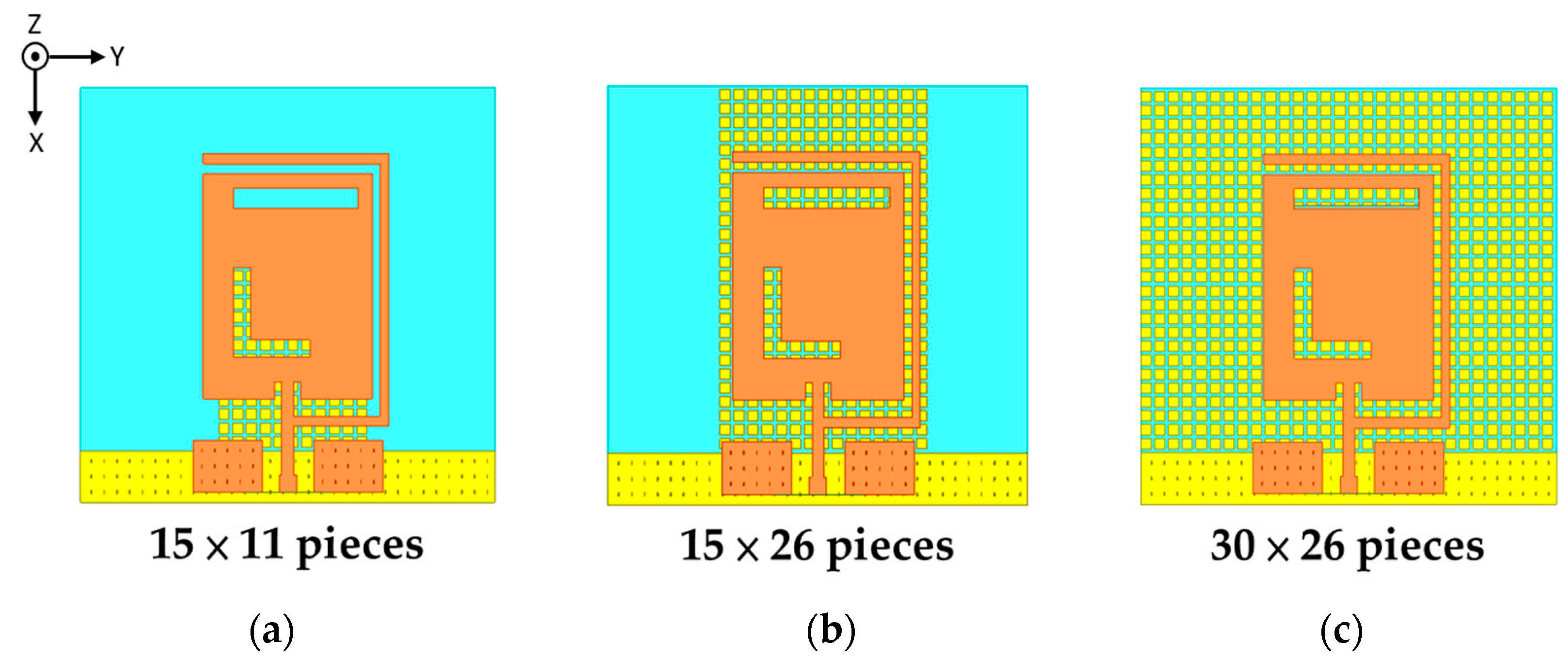
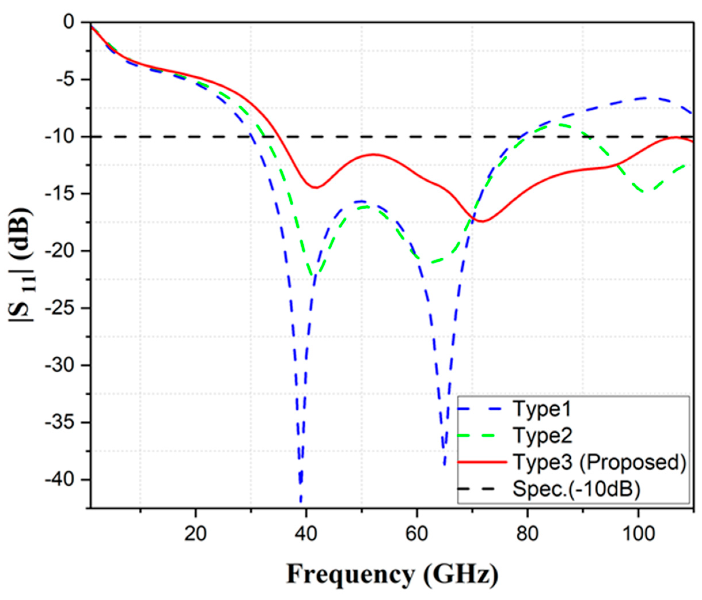
2.3. Parameter Analysis of the Number of AMCs
Then, this paper introduces the artificial magnetic conductor for simulation analysis to observe the influence of the number of artificial magnetic conductors on the radiation efficiency. The evolution of the number of artificial magnetic conductors and the simulation results are shown in
Figure 12a–c and
Figure 13. In
Figure 12a, the artificial magnetic conductor is located under the antenna, and the number was 15 × 11, with a bandwidth of 30.1 GHz to 78.8 GHz. There were resonance points at 39 GHz and 65 GHz, which were −41.9 dB and −38.6 dB, respectively.
Figure 12b’s artificial magnetic conductor extended from the bottom of the antenna to the front of the antenna, and the number was 15 × 26, with a bandwidth of 32.4 GHz to 79.9 GHz and 90.9 GHz–110 GHz. The resonance points were −22.1 dB at 41 GHz, −21 dB at 62 GHz, and −14.8 dB at 62 GHz. Compared with
Figure 12a, there was an additional 19.1 GHz frequency band. The number of artificial magnetic conductors in
Figure 12c was 30 × 26, covered with metal_1. At this time, the bandwidth was 34.8 GHz–110 GHz. There were resonance points at 42 GHz, 72 GHz, and 95 GHz, which were −14.4 dB, −17.4 dB, and −12.6 dB, respectively. Compared with
Figure 12b, it had a maximum bandwidth of 75.2 GHz. According to the simulation results,
Figure 12c had the best result when the artificial magnetic conductor increased.
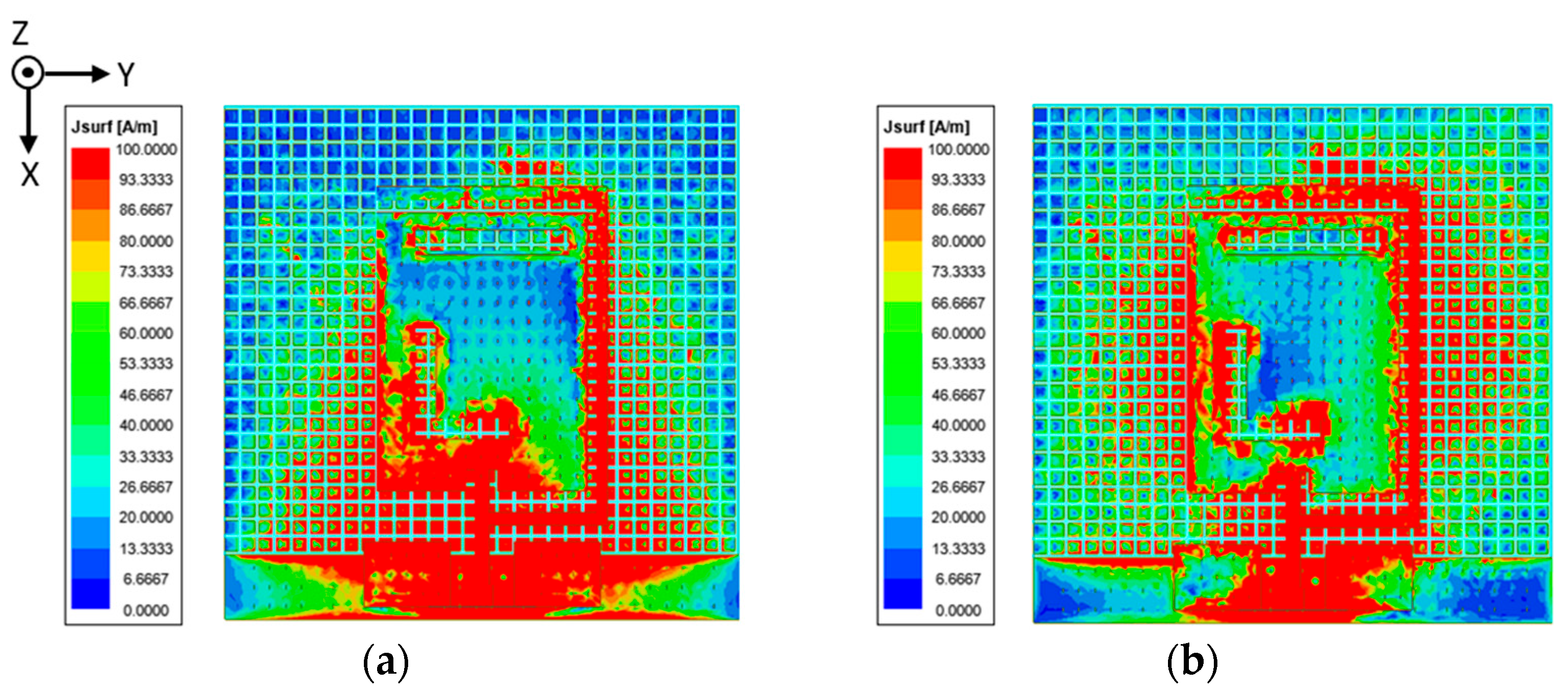
2.4. Current Distribution
Figure 14a,b show the current distribution of the antenna at 42 GHz and 72 GHz and analyze the structure operation of the antenna. This paper used the GSG probe to feed in, and the current was distributed to the antenna through the feed line. As shown in
Figure 14a, the current entered from the feeder line and was mainly distributed to the lower half of the patch antenna, part of the inverted C branch and L-shaped slot resonance, while the AMC current was more concentrated near the feeder line. In
Figure 14b, the current was distributed mainly to the entire inverted C branch and excited around the transverse and L-shaped slot. The current distribution of the AMC was more concentrated under the antenna body.
3. Results
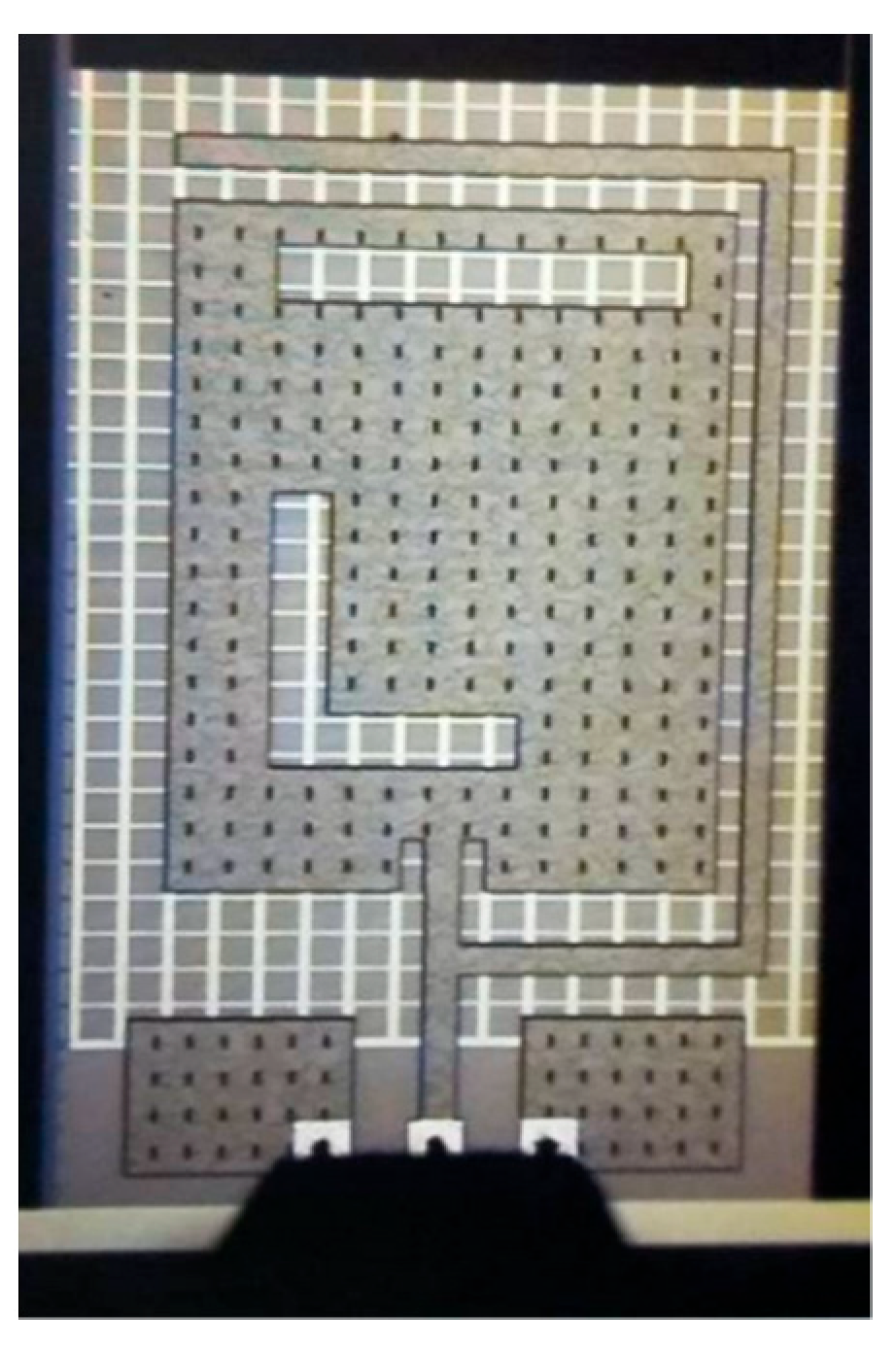
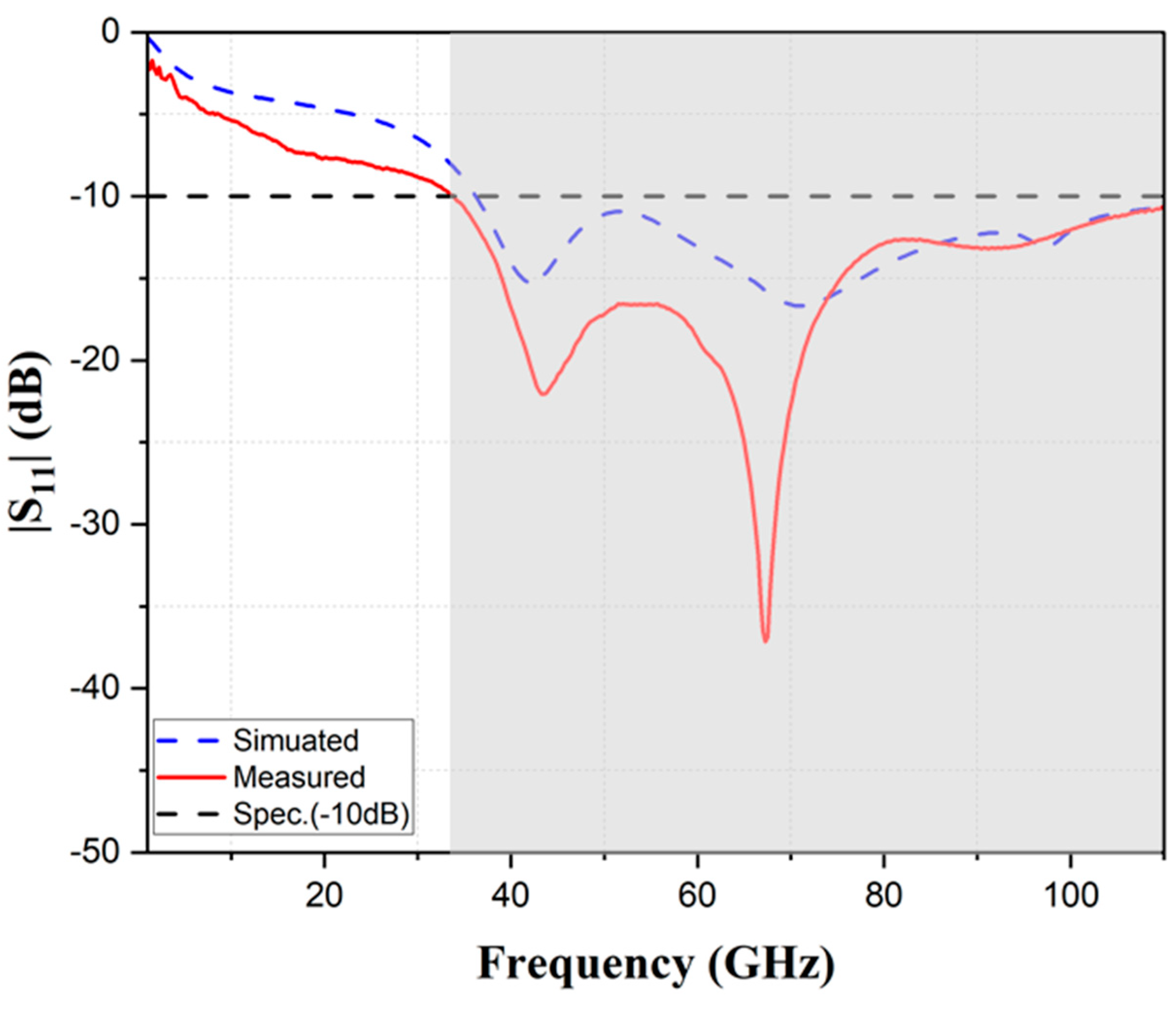
To verify the design results, the reflection coefficient of the proposed antenna was measured.
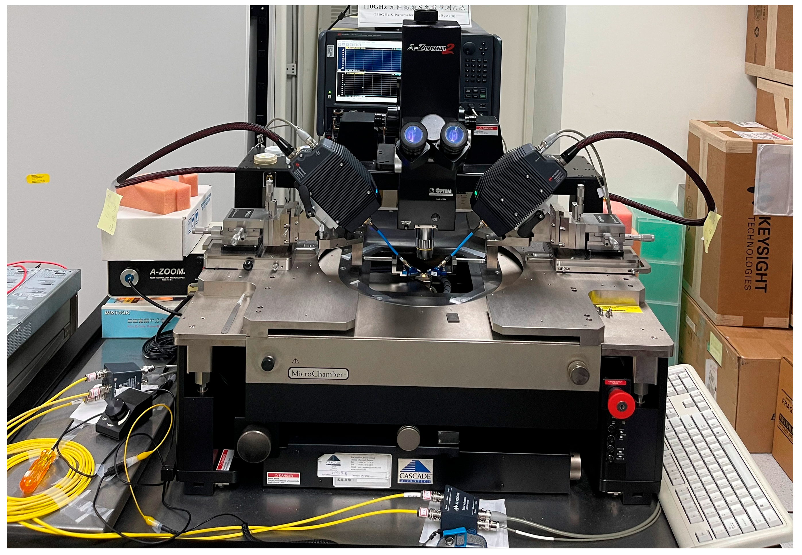
Figure 15 shows the micrograph of the chip antenna under measurement. The instrument used for measurement was the Keysight N5291A vector network analyzer, shown in
Figure 16 with SOLT calibration and a measuring range of 10 MHz–120 GHz. The measurement results were obtained by feeding the GSG probe, as shown in
Figure 17. Under the standard of −10 dB return loss, the measurement operating frequency could reach 33.8 GHz–110 GHz, which achieved up to 103.4% fractional bandwidth. The trend of simulation and measurement results was similar, but the measured results had a better reflection coefficient, which may have been caused by the impedance-matching effect of the lower needle measurement.
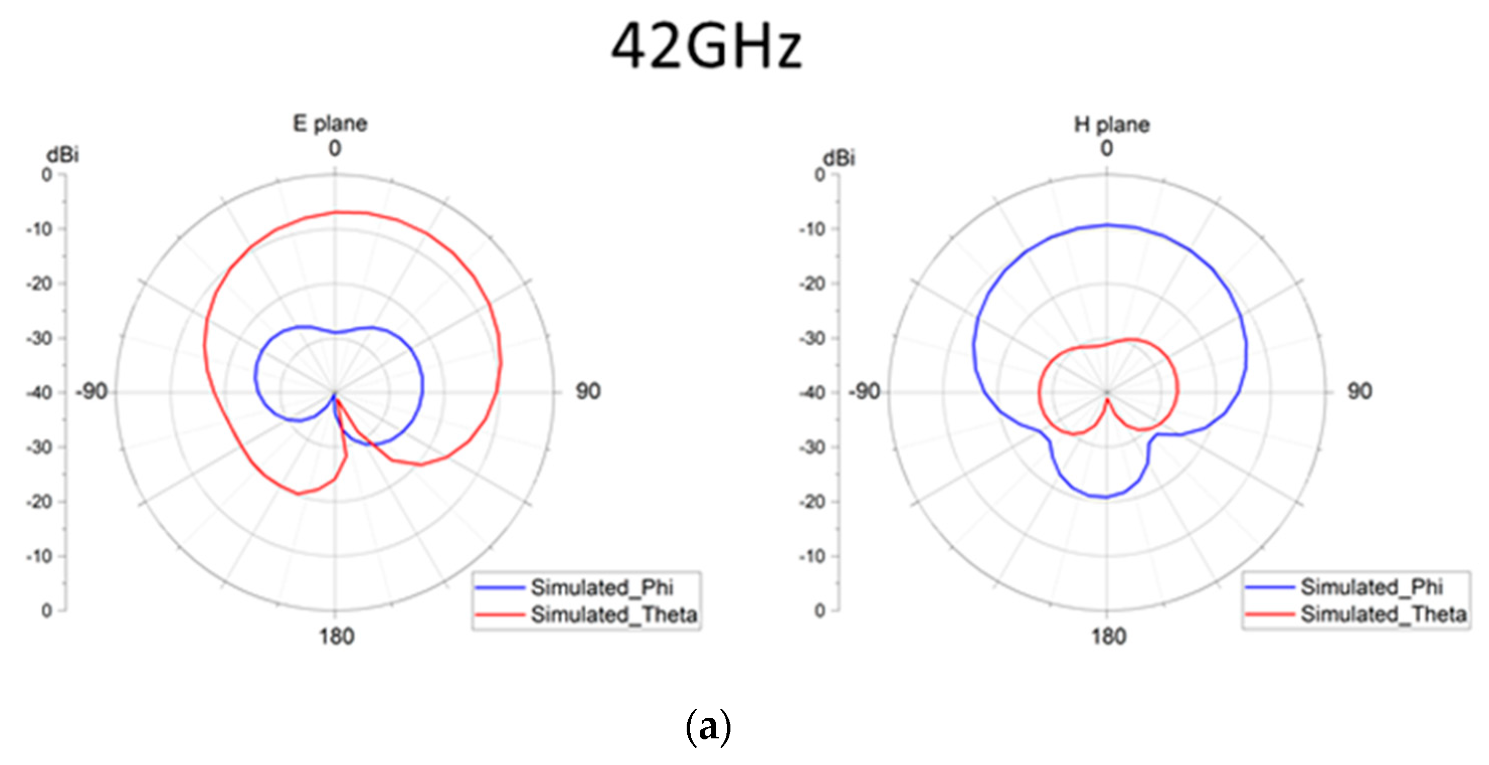
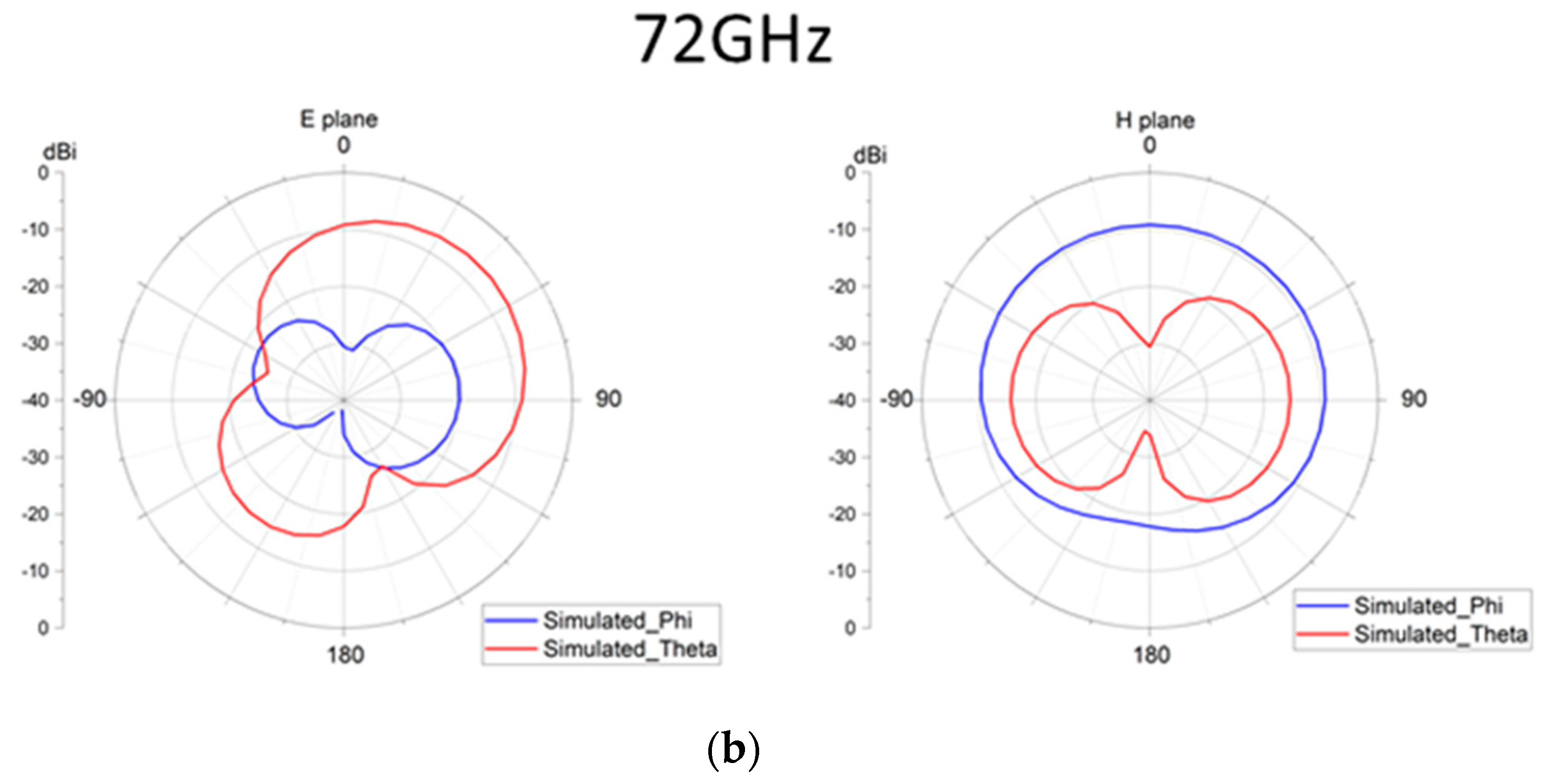
In order to understand the peak gain and field pattern,
Figure 18 shows the E and H planes of 42 GHz and 72 GHz. As shown in
Figure 18a, when the frequency was 42 GHz, it can be seen from the E-plane that the maximum gain was −6.3 dBi at a Theta angle of 30 degrees, and the maximum gain was −23.7 dBi at a Phi angle of 70 degrees. From the H plane, we can see that the maximum gain of the Theta plane was −26.9 dBi at 80 degrees, and the maximum gain of the Phi plane was −9.2 dBi at 0 degrees.
Figure 18b shows the field pattern at 72 GHz. From the E plane, it can be seen that the maximum gain was −6.4 dBi at a Theta angle of 50 degrees and −19.6 dBi at a Phi angle of 70 degrees. From the H plane, we can see that there was a maximum gain of −15.4 dBi at a Theta angle of 80 degrees and a maximum gain of −8.8 dBi at a Phi angle of 0 degrees.
5. Conclusions
A chip antenna is a good candidate for millimeter wave system applications requiring high integration and broadband characteristics. This paper proposed a small-size broadband antenna which was suitable for a millimeter wave system, using a 0.18 μm CMOS process, with size 1.2 × 1.2 (mm2). Metal_6 layer was used as the antenna design, and the Metal_1 layer introduced a square patch and ground plane to form the AMC structure. According to the parameter analysis, when the AMC was covered with the Metal_1 layer, 103.4% bandwidth could be obtained. In addition, the technology of the strip, L-shaped slot, and additional C branch was also used to increase the bandwidth of the antenna. The bandwidth of the proposed antenna is 34.8 GHz–110 GHz, which achieved 103.4% bandwidth. The actual measured bandwidth was 33.8 GHz–110 GHz, and the simulation and measured bandwidth were similar. It had a peak gain of −6.3 dBi at 72 GHz. The chip antenna proposed in this paper covers the 5G NR FR2 band (24.2 GHz–52.6 GHz) and W-band (75 GHz–110 GHz), which can be applied to the Internet of Things, Industry 4.0, biomedical electronics, near-field sensing and other fields. Its small size makes it easy to integrate with other microwave circuits, and it can form a highly integrated millimeter wave system. In the future, it will be able to integrate with microwave circuits or combine with printed circuit boards to improve the antenna gain performance further.


