Article

Microwave Photon Emission in Superconducting Circuits

1
INFN—Laboratori Nazionali di Frascati, 00044 Frascati, Italy
2
Istituto di Fotonica e Nanotecnologie CNR, 00156 Roma, Italy
3
INRiM—Istituto Nazionale di Ricerca Metrologica, Strada delle Cacce, 10135 Turin, Italy
4
INFN—Trento Institute for Fundamental Physics and Applications, Via Sommarive, 38123 Povo, Italy
5
Politecnico di Torino, Corso Duca degli Abruzzi, 10129 Turin, Italy
6
Fondazione Bruno Kessler, Via Sommarive, 38123 Povo, Italy
7
Istituto di Fotonica e Nanotecnologie CNR, Via Sommarive, 38123 Povo, Italy
*
Author to whom correspondence should be addressed.
Instruments 2023, 7(4), 36; https://doi.org/10.3390/instruments7040036
Submission received: 13 July 2023 / Revised: 26 October 2023 / Accepted: 27 October 2023 / Published: 30 October 2023

Abstract

:
Quantum computing requires a novel approach to store data as quantum states, opposite to classical bits. One of the most promising candidates is entangled photons. In this manuscript, we show the photon emission in the range of microwave frequencies of three different types of superconducting circuits, a SQUID, a JPA, and a JTWPA, often used as low-noise parametric amplifiers. These devices can be operated as sources of entangled photons. We report the experimental protocol used to produce and measure microwave radiation from these circuits, as well as data simulations. The collected spectra are obtained by performing single-tone measurements with a direct rf pump on the devices; the output spectra at low powers (below 100 dBm) are well interpreted by the dynamical Casimir model, while at high powers (above 100 dBm) the system is well described by the Autler–Townes fluorescence of a three-level atom.

1. Introduction

Josephson junctions (JJs) [1,2] are a strategic component of superconducting quantum circuits and will have an increasingly important role in the development of practical quantum technologies. They can be used in a wide variety of applications. Standalone JJs can be employed as single microwave photon detectors for axion dark matter search [3,4]. JJs are the building block of superconducting qubits, as well as more complex quantum circuits, such as superconducting circulators and quantum limited amplifiers [5,6].
Another important application for JJ-based devices is that of entangled photon generation [7,8]. The interest in entangled photon emitters lies in their potential to enable new types of quantum technologies. For example, entangled photon pairs can be used to perform secure quantum communication or quantum operations such as teleportation and error correction in quantum computing [9]. The study of the emission properties of quantum circuits is therefore extremely important since it enables the achievement of better control over entangled photons generation.
Phenomena such as electromagnetically induced transparency or Autler–Townes have been proposed as mechanisms to engineer the light propagation of superconducting circuits [10]. In this framework, we aim to study the emission properties of some of the fundamental superconductive devices in the GHz range, such as Superconducting Quantum Interference Devices (SQUIDs), Josephson Parametric Amplifiers (JPAs) and Josephson Traveling Wave Parametric Amplifiers (JTWPAs).
SQUIDs and JPAs are among the most relevant JJ-based superconducting circuits for sensing and amplification [11]. SQUIDs are initially born as extremely sensitive magnetometers, capable of detecting magnetic fields as low as 10 15 T [12], but can also be employed as low-noise microwave amplifiers in the MHz−GHz range [11]. JPAs are an enabling technology for superconducting qubit measurements [13], due to their high fidelity readout [14], and are, at this point, massively used in superconducting quantum information processing [15]. They usually work in the GHz range of frequency [16].
Recently, in the last decade, first SQUIDs and then JPAs have become the paradigm of cold-stage preamplification in light dark matter searches, such as axions and axion-like particles [17,18,19], since they give a significant improvement in the noise temperature compared to the cold semiconductor amplifiers (such as HEMTs) in the microwave range of frequencies. In fact, the noise temperature of SQUIDs is within a factor 2 of the standard quantum limit (SQL) below a physical temperature of 70 mK [20], T SQL = h ν / k B , while JPAs are only slightly above the SQL, offering the possibility to reach the required sensitivity and signal-to-noise ratio in these type of searches.
In this paper, we present radiofrequency measurements on a SQUID and a JPA, showing their peculiar nonlinear nature. In particular, we show the possibility of using the devices as photon emitters since they exhibit the generation of couples of photons when driven with a single pump tone. Our interpretation of the results is twofold: we compare the data to the dynamical Casimir effect (DCE) [21,22,23] and to the Autler–Townes [24,25,26,27] fluorescence in three-level artificial atoms.
Additionally, we also present the same technique applied to JTWPAs, which are being developed and tested to serve in many fields [11], such as in quantum information processing, radio-astronomy, and dark matter searches [28]. Compared to JPAs, JTWPAs are characterized by a wider bandwidth (few GHz) and higher saturation power (>−90 dBm), at the price of more complex circuitry and a slightly higher noise level [29]. We believe that the DCE interpretation of the data is applicable to the JTWPA as well; however, precise quantitative modeling is left for future works.

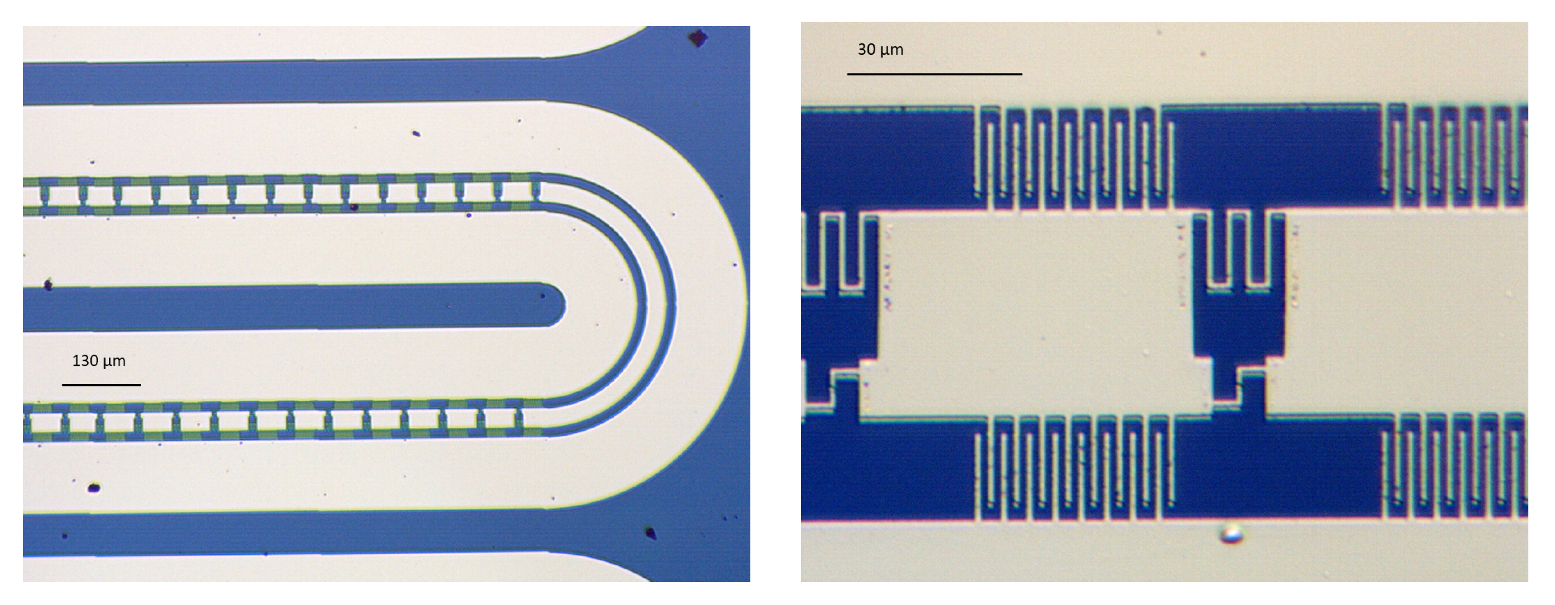
2. Devices and Experimental Setup

2.1. SQUID

The chip for this device (Figure 1) contains a simple CPW (Coplanar Waveguide) transmission line ended with a dc-SQUID. Area, critical current, and capacitance of a single junction in the dc-SQUID are approximately A = 4 μ m 2 , I c = 1.5 μ A and C J = 0.59 pF, respectively. More details on these parameters can be found in previous works [4,30]. The dc bias and rf pumping are obtained thanks to a coil printed on the chip next to the SQUID.
The junctions are fabricated using the shadow mask evaporation technique. A lift-off stencil is obtained by using electron beam lithography on a resist bilayer (in our case, PMMA 6% AR-P 669.06/on COP 33 10% AR-P 617.12). Some of the underlying polymer is removed due to its different sensitivity, forming the overhang. After the first angled Al evaporation ( 155 deg ), an oxidation step follows (2.5 mbar for 5 min). A second Al evaporation is performed at 90 deg to define the tunnel junctions.
The experimental scheme for the SQUID is shown in Figure 2 (top left) —refer to Table A1 of Appendix A to know microwave components details. Here, the dashed lines indicate all the temperature stages of the cryostat, and the device is housed in the 10 mK stage. Two input coaxial cables send rf signals to the device. One is connected to the rf signal generator (S1), which is used as the pump tone generator, the other is connected to one port of a Vector Network Analyzer (VNA), which is used to send probe signals. Attenuators are shown with their attenuation value in dB units and are necessary to reduce the thermal noise at the device input. The rf sent from S1 and the VNA are combined at room temperature through a directional coupler and then travel on the same input line to the SQUID, passing through a bias tee (BT in Figure 2), which serves to simultaneously send radiofrequency and dc current to the device. The output line relies on a low-noise HEMT amplifier at the 4 K stage and an FET amplifier at room temperature, each giving 30 dB of amplification. Finally, the output signal is split and redirected to the readout port of the VNA and to a spectrum analyzer. The red segments on the transmission lines indicate superconducting coaxial cables. The lines indicated as “Aux” are auxiliary lines used for calibration purposes and are accessible thanks to a cryogenic switch mounted on the 50 mK plate. Additionally, the “rf bias” (S2) line indicated in the figure is used to send the rf flux bias on the coil. All the dc bias lines possess 1 MHz low-pass (LP) filters. The “Voltmeter” depicted in the scheme indicates that the voltage across the SQUID is detected; this is necessary for IV characteristics and escape distributions measurements.
For the SQUID, we estimated the attenuation of the input line from room temperature measurements without taking into account the superconducting segment. The reference value at 10 GHz is 83 dB when measured from the VNA port, and 73 dB when measured from the pump generator due to the 10 dB difference in the attenuations of the directional coupler ports.

2.2. JPA

The JPA device (Figure 3) is designed as a flux qubit [31,32] and is composed of a CPW transmission line coupled to a λ / 4 coplanar resonator of length l = 2.6 mm through an interdigital capacitance of 10 fF. The bare resonator frequency is ω 0 r = 11.35 GHz. Then, the resonator is ended with a dc-SQUID which junctions have C J = 0.4 pF and I c = 0.47 μ A, resulting in a plasma frequency of ω 0 J / 2 π = 9.24 GHz. For completeness, we report that this sample device showed a gain of G = ( 15.5 ± 2.0 ) dB at the frequency of 7.42 GHz, with a bandwidth of 5 MHz when pumped with double the signal frequency and biased with a flux Φ = 0.19 Φ 0 .
The fabrication of the Josephson junctions forming the dc-SQUID relies on the Niemeyer–Dolan technique [33], exploiting suspended Dolan-bridges and a double-angle aluminum evaporation step. The complete microfabrication process can be summarized as follows. A 150 nm thick aluminum film is sputter-deposited on a 6 high-resistivity silicon wafer (FZ silicon wafers, diameter: 6 , thickness: 625 ± 15 μ m , dopant: Boron (type p), orientation: <100>, resistivity: >8000 Ω / cm ). The film is patterned and plasma-etched to structure the resonator transmission line, the pump transmission line, and the dc-flux line. Subsequently, a second lithographic step is performed by preparing the suspended Dolan-bridges. The shadow evaporation process for the microfabrication of the Josephson junctions is performed with a tilting angle of 30 , depositing 50 nm and 60 nm of aluminum before and after the oxidation step, respectively. The oxidation dose is given by a pressure in the evaporator chamber of 2 Pa and an oxidation time of 2 min and 24 s. Such parameters are expected to yield a specific resistance of the single Josephson junction of about 346 Ω μ m 2 , as confirmed by dc electrical measurements performed on test dc-SQUID devices produced on the same wafer.
Each chip features a size of 10 mm × 2.5 mm, and it comprises two JPA devices, as shown in Figure 3. The JPA devices on the same chip differ in the size of the Dolan-bridges and, thus, in the difference in the areas of the Josephson junctions. The expected critical current value of the dc-SQUID of the JPA device that has been tested is about 1.8 μ A.
The rf scheme is quite similar to that in Section 2.1, except for some details (Figure 2 top right). In fact, here, the HEMT and FET amplifiers give, respectively, 36 dB and 35 dB of amplification, and a circulator has been added to the HEMT output for better isolation. Attenuators’ positions and values change according to the new scheme. The dc bias lines only supply current to the coil, and the low-pass filters are removed.
Here, the cryogenic switch allows for all the necessary combinations between lines for calibration purposes. A system of equations with the input, output, and auxiliary lines as unknown terms has been solved, where the known terms are the S21 parameters of the combinations input-output, input-Aux1, Aux1-Aux2, and Aux2-output. The only segment that does not enter the equations is the one from the JPA to the circulator, whose attenuation has been measured separately at room temperature. Since the calibration procedure is not fully self-consistent, we attributed a 2 dB uncertainty to the results. Thus, the attenuation of the input line at the reference frequency of 7.25 GHz is ( 75 ± 2 ) dB if measured from the VNA port, and ( 85 ± 2 ) dB if measured from the signal generator (due to the additional 10 dB in the coupled port of the directional coupler).

2.3. JTWPA

The JTWPA design follows the coupled mode equations developed in Refs. [34,35] and is optimized to avoid power leakage and improve the phase matching. It is composed of 15 sections of a CPW embedding 990 nonhysteretic rf-SQUIDs connected by bent sections of CPW. The values of the circuit parameters of the Josephson metamaterial, by design, are a ground capacitance of C g = 13.0 fF, a geometrical inductance L g = 45 pH, a Josephson capacitance of C J = 25.8 fF and a Josephson critical current of I c = 1.5 μ A . The Josephson junctions were fabricated by exploiting an electron beam lithography process on a double-layer polymeric mask, followed by an aluminum e-gun evaporation. The JTWPA is shown in Figure 4. The gain of this prototype device reached up to 25 dB with a signal frequency of 9 GHz when pumped at 18 GHz (degenerate mode) and up to 20 dB when pumped at 13.4 GHz (nondegenerate mode). All the details are present in [36].
The experimental setup for the JTWPA measurements is presented in Figure 2 (bottom). The device temperature during measurements settled at about 15 mK. In this case, two different input transmission lines are used to send radiofrequency to the device. One is connected to the rf pump tone generator (S1), and the other is connected to one port of the VNA. The pump and signal lines are then coupled together on the same line thanks to the directional coupler at the 10 mK stage. The JTWPA receives both microwaves and a dc bias current thanks to the two bias tees. The cryogenic switch mounted on the 50 mK plate allows us to test the device both in reflection and in transmission. Then, on the output line, the HEMT amplifier at the 4 K stage provides 30 dB of amplification.
Also, in this case, we measured the scattering parameters of each line at room temperature to calibrate the system. From these parameters, an estimation of attenuation values was given for the signal line from port 1 of the VNA, which is 72 dB at 9 GHz, and for the pump line, which is 65 dB at 18 GHz. These values are given at the reference frequencies where signal and pump were operated ( f p = 2 f s ).
All the Josephson devices tested are put in a magnetic shield composed of a lead box covered with a foil of Mu-metal, so we expect that the external magnetic field is properly shielded.

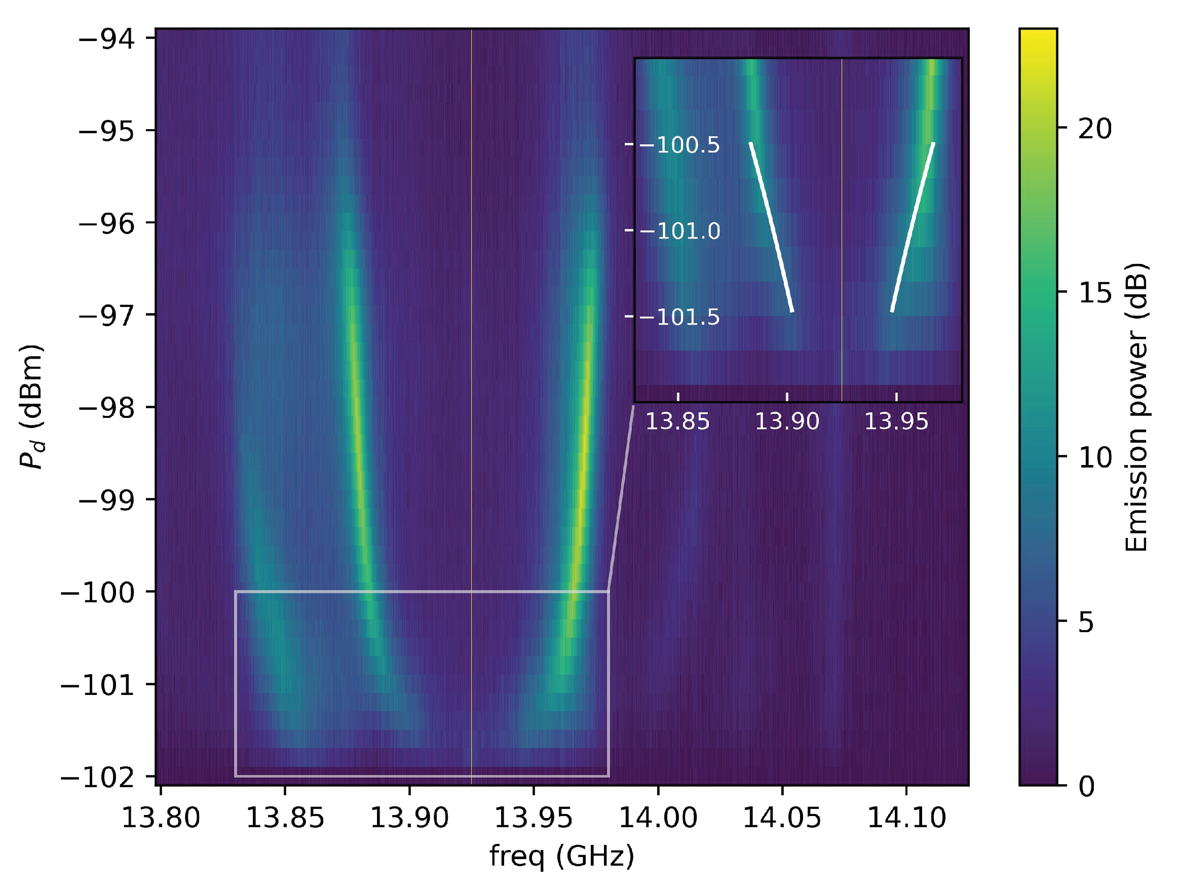
3. Results and Discussion

3.1. SQUID

Referring to the scheme of Figure 2 (top left), the experiment is conducted by sending a single pump tone from the signal generator (S1) to the SQUID and reading the response to it with a spectrum analyzer, after having properly amplified the output signal. As the device has only one rf port, the measurements are taken in reflection mode. Figure 5 shows the results of the SQUID response. The plot is obtained by keeping the drive frequency fixed at ω d / 2 π = 13.93 GHz and changing the drive power P d . The values of the y-axis refer to the power at the device input after calibration. The output photons are divided into two branches, with their peak frequencies symmetric with respect to the drive frequency, which means conservation of the photon energies, ( ω 1 + ω 2 ) / 2 π = 2 ω d / 2 π .
The low-power region of the spectrum has been interpreted as the emission due to the dynamical Casimir effect (DCE) [21,22,23], which has been modeled for our scheme in Appendix B. In Figure 5, the white lines in the inset show the behavior of the SQUID under the direct pump drive as predicted by the DCE, superimposed to the data. In the calculations, we start from the Lagrangian of a CPW and end with a SQUID, which is driven by microwaves parametrized as a flux field on the transmission line, and after finding the equation of motion, we calculate the output number of photons as the expectation value of the output field on the vacuum state (Equation (A24)). The resulting output spectrum is shown in Equation (A26):
n out ( ω ) = ω 4 π Z 0 δ ( ω ω d ) Φ 0 2 π δ E J 2 E J 0 Φ 0 2 π 2 A ω d 2 C J E J 0 · D ( ω ) 2 + + δ E J 2 E J 0 ω 2 ω d ω Θ ( 2 ω d ω ) 2 i k 2 ω d ω L e f f 0 · D ( 2 ω d ω ) · D ( ω ) 2 ,
with D ( ω )
D ( ω ) = 1 1 C J ω 2 E J 0 Φ 0 2 π 2 i k ω L e f f 0 .
The first term represents the drive tone reflected back on the transmission line, while the second term gives rise to two distributions, one peaked in the SQUID plasma frequency ω J ( P d ) (which is contained in the factor D ( ω ) of Equation (A27)), and another peaked in 2 ω d ω J ( P d ) . Note that the plasma frequency has a dependence on the drive amplitude through the definition of the energy E J 0 (Equation (A19)):
E J 0 = 2 E J δ E J , δ E J = A 2 2 E J 2 π Φ 0 2 .
This is exactly the dependence, giving the variability of the simulated curves in Figure 5 explaining the linear regime of the data. In fact, increasing the drive amplitude, E J 0 decreases and both ω J and ( 2 ω d ω J ) increase, and consequently, the two output branches move away. Note, however, that this behavior is only valid at small drive powers, and the result of Equation (A26) can only predict the linear regime (below 95 ± 2 dBm the contribution of the quadratic term in the cosine expansion of Equation (A17) is less than 1%). To account for the saturation at higher powers, we should also include higher-order terms in the approximations.
For the high-power region of the emission spectrum, a possible interpretation is given by the generation of Autler–Townes (AT) splitting. In a multi-level system, when a transition between two levels is driven by a strong drive, the dressed states can be viewed as split states [24]. This is the AT splitting, and it can be spectroscopically investigated, probing the transition to a third level of the system. In our case, we can consider the SQUID as an artificial atom with three levels, | 0 , | 1 , | 2 . In a canonical AT experiment, two tones are simultaneously sent to the device with frequencies almost resonant with the single photon transition | 0 | 1 , and | 1 | 2 called ω p and ω c [25]. In this configuration, ω p dresses the | 1 state and at the same time ω p + ω c excite the artificial atom in | 2 . The photons emitted as consequence of the decay | 2 | 1 | 0 have energies ω 10 ± Ω R / 2 [26] as illustrated in Figure 6 (left), where Ω R is the Rabi frequency. The probe tone ω p is usually almost resonant with the transition ω 10 and can be written as ω 10 = ω p + Δ p , with Δ p being the detuning between ω 10 and ω p . The same relation holds for ω c and ω 21 : ω 21 = ω c + Δ c where Δ c is the detuning between ω 21 and ω c . The Hamiltonian for this system written in the SQUID eigenstates basis and using the RWA is [27]: H = n = 1 2 ω n | n n | + Ω p cos ( ω p t ) | 1 0 | + Ω c cos ( ω c t ) | 2 1 | , where ω n is the n-th eigenvalue of the artificial atom, Ω p and Ω c are the amplitudes of the two driving fields.
In our case, we send a single tone to the SQUID. However, since the power arriving at the device is large, it is possible that single- and multi-photon absorption channels are open concomitantly. In this case, ω p = ω c and single photon absorption and K photons absorption are allowed. This scenario can be modeled as sending K different drives, each with frequency ω p and amplitude Ω K . The detuning of each drive can be expressed recursively as a function of the detuning Δ p and of the anharmonicity of the system. We assume that in a weakly anharmonic system the relation E n , n 1 E n + 1 , n = α holds, where α is the system anharmonicity and E n , n 1 is the energy difference between the energy levels E n and E n 1 . The detuning Δ n of the n-th tone with respect to the energy ω n , n 1 can be expressed as: Δ n = Δ n 1 α (with Δ 1 = Δ p ). Assuming multi-photon absorption, it is necessary to take into account higher levels above level | 2 . Using the approach of Ref. [25] the Hamiltonian of the system becomes:
H = n = 1 N i = 1 n Δ i | n n | + Ω n 2 | n n 1 | + h . c . ,
where i = 1 n Δ i = n Δ p + α n ( n 1 ) 2 . We consider the energy levels up to | 4 , thus here N = 4 . The output power spectrum is constructed by numerically solving the Liouville equation choosing as decay rates Γ 10 / 2 π = Γ 21 / 2 π = 2.5 MHz and Γ 43 / 2 π = Γ 32 / 2 π = 1 MHz. We then chose as initial state | 0 and as final state | 2 . We calculated the Fourier transform of their correlation function to obtain the emission spectra [25]. The simulated output spectrum as a function of the drive power is shown in Figure 6 (right). It reflects fairly well the splitting dispersion as a function of the drive power of the two main branches of the data as well as the peaks linewidths. The appearance and the trend of the sidebands around 13.85 and 14 GHz in Figure 5 may be due to the simultaneous detection of AT doublet and Mollow triplets. In fact, the sideband frequency separation is roughly 2 Ω R [26]. The appearance of the sidebands is almost vanishing in our simulation, suggesting that a more accurate model of the energy levels anharmonicity should be adopted.

3.2. JPA

The experiment is conducted in the same way as in Section 3.1, and the JPA is also measured in reflection mode. The results are shown in Figure 7. In the power dependence, the peaks separation is about 250 MHz, and here the linear regime is not visible. This setup is equal to the open resonator circuit described in Ref. [21].
The data from Figure 7 do not show an observable low power signal as in the case of the SQUID (note that the power scales are different in the two cases). On the other hand, the high power region of the spectrum is clearly visible and was simulated using the Hamiltonian of Equation (1) for AT-like emission. The simulation result shown in Figure 8 is in good agreement with the spectrum in Figure 7. For the JPA we used as decay rates Γ 10 / 2 π = Γ 21 / 2 π = 2.5 MHz and Γ 43 / 2 π = Γ 32 / 2 π = 1 MHz, which are comparable with the S21 linewidth of 4 MHz. Lacking any effect at lower power, we did not consider the DCE approach here.

3.3. JTWPA

The same type of measurements were conducted on a JTWPA, which has two ports enabling the reading of both reflection and transmission signals. The results for the transmission data are presented in Figure 9 (results for reflection mode are identical). Qualitatively, we observe photon splitting in this case as well, which can be attributed to internal reflections driven by the pump. The reflection coefficient describes the behavior of the transition between the 15 linear sections and the 50 Ohm CPW curves of the JTWPA. This complex condition can be modeled as a series of semi-transparent mirrors, moving as a consequence of the pump drive (in analogy to solid state with a pump-induced time-varying refractive index; for our device, we have a time varying impedance). Then, the traveling tones in the metamaterial experience the presence of these moving mirrors as in the DCE. Given the intricacy of the JTWPA system, it is more challenging to derive a precise and quantitative interpretation of the data. Hence, we leave room for further investigation.

4. Conclusions

We investigated the generation of photons in three superconducting circuits, in particular a SQUID, a JPA, and a JTWPA, when they are driven by a single tone of monochromatic microwaves. The paper focused on the method of performing these types of radiofrequency measurements, with particular attention to the experimental setup and the description of microwave components. The response of the devices to a pump tone presents two photon distributions symmetric with respect to the rf drive, in which frequency spacing increases along with the power. The SQUID and JPA setups are very similar to the systems used to reproduce a mirror with variable boundary conditions, which generate the dynamical Casimir radiation, and the simulations of the DCE are comparable with the experimental spectra at low powers. The results at high power levels are well interpreted by the Autler–Townes fluorescence of a multi-level system in the presence of multi-photon absorption. As a further development, we aim to study these devices as generators of entangled photons as demonstrated in Ref. [8]. This topic will be treated in future works.

Author Contributions

Formal analysis, A.R. and A.D.; investigation, A.R., F.C., A.D., D.D.G., C.G., C.L., G.M., F.M. (Francesco Mattioli) and S.T.; resources, F.C., E.E., L.F., F.M. (Federica Mantegazzini), B.M., F.M. (Francesco Mattioli) and A.V.; software, F.C., A.D. and A.R.; writing—original draft preparation, A.R. and A.D.; project administration, C.G.; writing—review and editing, all authors. All authors have read and agreed to the published version of the manuscript.

Funding

This research was partially funded by the PNRR MUR project number PE0000023-NQSTI.

Data Availability Statement

The data are available upon reasonable request to the authors.

Acknowledgments

The authors wish to thank Danilo Babusci for having checked and corrected the calculations of Appendix B; the authors are also thankful to Luca Piersanti and Matteo Beretta for giving constant support to the laboratory.

Conflicts of Interest

The authors declare no conflict of interest.

Appendix A. Rf Components Details

Table A1. Names, models, and working frequency ranges of rf components shown in Figure 2.
InstrumentModelBandwidth
VNAAgilent E5071C300 kHz–20 GHz
Signal generator (S1)Rohde&Schwarz SMA100B8 kHz–20 GHz
Signal generator (S2)Rohde&Schwarz SGS100A1 MHz–12.75 GHz
Spectrum AnalyzerSignal Hound SM200B100 kHz–20 GHz
FET +30 dBNarda Miteq LNA-30-08001200-09-10P8 GHz–12 GHz
FET +35 dBNarda Miteq LNA-30-04001200-15-10P4 GHz–12 GHz
HEMT +30 dBLow Noise Factory LNF-LNC6_20C s/n 1403Z6 GHz–20 GHz
HEMT +36 dBLow Noise Factory LNF-LNC4_16B s/n 2157Z4 GHz–16 GHz
Attenuators (A1)Radiall R413806000/R411810121/R411820121DC–18 GHz
Attenuators (A2)Narda Miteq 4768-6/4768-10/4768-20DC–40 GHz
Directional CouplerMini-Circuits ZUDC10-02183-S+2 GHz–18 GHz
Circulators (C1)Low Noise Factory LNF-CIC4_12A4 GHz–12 GHz
Double circulator (C2)Quinstar Technology QCY-G08012028 GHz–12 GHz
Bias Tee (BT)Marki Microwave BT-001840 kHz–18 GHz
SwitchRadiall R577443005DC–18 GHz
SplitterMini-Circuits ZX10-2-183-S+1.5 GHz–18 GHz

Appendix B. Derivation of SQUID Resonances with Direct Pump Drive

We derive the SQUID response following the calculations of Ref. [21]. The device is the same, so we start from the Lagrangian of Equation (4) of Ref. [21]:
L = 1 2 i = 1 Δ x C 0 ( Φ ˙ i ) 2 ( Φ i + 1 Φ i ) 2 Δ x L 0 + j = 1 , 2 C J , j 2 ( Φ ˙ J , j ) 2 + E J , j cos 2 π Φ J , j Φ 0 .
The symbols are as follows: Δ x represents the unit length of a transmission line; C 0 and L 0 are, respectively, the characteristic capacitance and inductance per unit length of the CPW; C J , j and E J , j are the capacitance and Josephson energy of the jth junction in the SQUID; Φ α is the node flux and is related to the phase ϕ α at the node α as Φ α = ( Φ 0 / 2 π ) ϕ α ; Φ 0 = h / 2 e is the magnetic flux quantum. A flux variable for the SQUID is introduced, Φ J = ( Φ J , 1 + Φ J , 2 ) / 2 , but the fluxes are also related to the external magnetic flux: Φ J , 1 Φ J , 2 = Φ ext . Solving these equations together one obtains:
Φ J , 1 = Φ J + 1 2 Φ ext Φ J , 2 = Φ J 1 2 Φ ext .
Moreover, the junctions are assumed to be identical, so that C J , 1 = C J , 2 = C J / 2 and E J , 1 = E J , 2 = E J . With these assumptions and inserting Equation (A2) into Equation (A1), and using the relation cos ( α ± β ) = cos α cos β sin α sin β , the Lagrangian becomes:
L = 1 2 i = 1 Δ x C 0 ( Φ ˙ i ) 2 ( Φ i + 1 Φ i ) 2 Δ x L 0 + C J 2 ( Φ ˙ J ) 2 + 2 E J cos π Φ ext Φ 0 cos 2 π Φ J Φ 0 ,
where we have exploited the fact that in our setup there is no applied external magnetic flux, so Φ ext = 0 , but we send a direct pump drive with a signal generator. Then, instead of only Φ J , we replace the flux as Φ t o t = Φ J + Φ d r in the capacitive term and in the cosine term. From now on, the energy term in Equation (A3) is different from that in Ref. [21] and is:
2 E J cos 2 π Φ J + Φ d r Φ 0 .
Making use again of the cosine and sine relations, the Lagrangian becomes:
L = 1 2 i = 1 Δ x C 0 ( Φ ˙ i ) 2 ( Φ i + 1 Φ i ) 2 Δ x L 0 + C J 2 ( Φ ˙ J + Φ ˙ d r ) 2 + 2 E J cos 2 π Φ J Φ 0 cos 2 π Φ d r Φ 0 sin 2 π Φ J Φ 0 sin 2 π Φ d r Φ 0 .
We define the two energy terms
E J c ( t ) 2 E J cos 2 π Φ d r ( t ) Φ 0 E J s ( t ) 2 E J sin 2 π Φ d r ( t ) Φ 0 .
In the hypothesis that Φ J / Φ 0 1 , expanding cos 2 π Φ J / Φ 0 at the second order and sin 2 π Φ J / Φ 0 at the first order the Lagrangian becomes:
L = 1 2 i = 1 Δ x C 0 ( Φ ˙ i ) 2 ( Φ i + 1 Φ i ) 2 Δ x L 0 + C J 2 ( Φ ˙ J + Φ ˙ d r ) 2 + E J c ( t ) 1 1 2 2 π Φ 0 2 Φ J 2 2 π Φ 0 Φ J E J s ( t ) ,
where we can drop the constant term E J c ( t ) since it will not enter the equation of motion. Now, the Hamiltonian is written as:
H = i L Φ ˙ i Φ ˙ i L = 1 2 i = 1 Δ x C 0 ( Φ ˙ i ) 2 + ( Φ i + 1 Φ i ) 2 Δ x L 0 + C J 2 ( Φ ˙ J 2 Φ ˙ d r 2 ) + 1 2 2 π Φ 0 2 Φ J 2 E J c ( t ) + 2 π Φ 0 Φ J E J s ( t ) .
The conjugate variables are Φ i , J and P i , J = L / Φ ˙ i , J , which satisfy the commutation relations Φ i , P j = i δ i , j and Φ i , Φ j = P i , P j = 0 . With these definitions and setting Φ J Φ 1 , the Hamiltonian becomes:
H = 1 2 i = 1 P i 2 Δ x C 0 + ( Φ i + 1 Φ i ) 2 Δ x L 0 + C J 2 Φ ˙ 1 2 Φ ˙ d r 2 + 1 2 2 π Φ 0 2 Φ 1 2 E J c ( t ) + 2 π Φ 0 Φ 1 E J s ( t ) .
The Heisenberg equation of motion (EOM) for the flux operator Φ 1 plays the role of a boundary condition for the field in the CPW. This is written as:
P ˙ 1 = C J Φ ¨ 1 + C J Φ ¨ d r = i P 1 , H .
Performing all the commutators and passing to the continuum limit Δ x 0 , by posing Φ 1 ( t ) Φ ( x = 0 , t ) , the resulting EOM becomes:
C J Φ ¨ ( 0 , t ) + C J Φ ¨ d r ( 0 , t ) + 1 L 0 Φ ( x , t ) x x = 0 + 2 π Φ 0 2 Φ ( 0 , t ) E J c ( t ) + 2 π Φ 0 E J s ( t ) = 0 .
Now we write the flux in the second quantized form as a sum of ingoing and outgoing waves in all the frequencies:
Φ ( x , t ) = Z 0 4 π 0 d ω ω a in ( ω ) e i ( k ω x + ω t ) + a out ( ω ) e i ( k ω x + ω t ) + h . c . ,
where Z 0 = L 0 / C 0 is the characteristic impedance of the CPW, k ω = ω / v , and the field operators satisfy the commutation relations
a in ( out ) ( ω ) , a in ( out ) ( ω ) = δ ( ω ω ) .
We define the Fourier Transform (FT) and the Dirac delta function as follows:
F ( ω ) = f ( t ) e i ω t d t , δ ( ω ω ) = 1 2 π e i ( ω ω ) t d t .
Substituting the definition of Equation (A12) into Equation (A11), and Fourier transforming all the terms (assuming ω > 0 ), the EOM becomes
C J ω 2 a in ( ω ) + a out ( ω ) + i k ω L 0 a in ( ω ) a out ( ω ) + + 2 π Φ 0 2 d ω g ( ω , ω ) Θ ( ω ) a in ( ω ) + a out ( ω ) + Θ ( ω ) a in ( ω ) + a out ( ω ) + + | ω | 2 π 4 π Z 0 2 π Φ 0 d t e i ω t E J s ( t ) + | ω | 2 π 4 π Z 0 d t e i ω t C J Φ ¨ d r ( t ) = 0 ,
where we have adopted the rotating wave approximation (RWA) and grouped the factor 2 π / | ω | . Θ ( ω ) is the Heaviside function and the g ( ω , ω ) factor is defined as
g ( ω , ω ) = 1 2 π | ω | | ω | d t e i ( ω ω ) t E J c ( t ) .
We now make explicit the terms E J c ( t ) and E J s ( t ) , expanding the sine and cosine in the hypothesis that Φ d r / Φ 0 1 :
E J c ( t ) = 2 E J cos 2 π Φ d r ( t ) Φ 0 2 E J 1 1 2 2 π Φ 0 2 Φ d r 2 ( t ) ,
and we write the drive as a plane wave Φ d r ( t ) = A cos ω d t . Note that Φ d r 2 ( t ) = A 2 cos 2 ω d t = A 2 ( 1 + cos 2 ω d t ) / 2 . Then:
E J c ( t ) 2 E J 1 1 2 2 π Φ 0 2 A 2 2 ( 1 + cos 2 ω d t ) = E J 0 δ E J cos 2 ω d t ,
with E J 0 and δ E J defined as
E J 0 = 2 E J δ E J , δ E J = A 2 2 E J 2 π Φ 0 2 .
The E J s ( t ) term is
E J s ( t ) = 2 E J sin 2 π Φ d r ( t ) Φ 0 2 E J 2 π Φ 0 Φ d r = δ E J cos ω d t ,
where δ E J = 2 E J A 2 π Φ 0 .
Inserting Equations (A19) and (A20) into Equation (A15), the boundary condition in the frequency domain is
0 = C J ω 2 a in ( ω ) + a out ( ω ) + i k ω L 0 a in ( ω ) a out ( ω ) + + 2 π Φ 0 2 E J 0 a in ( ω ) + a out ( ω ) 2 π Φ 0 2 δ E J 2 | ω | | ω + 2 ω d | a in ( ω + 2 ω d ) + a out ( ω + 2 ω d ) 2 π Φ 0 2 δ E J 2 | ω | | ω 2 ω d | Θ ( ω 2 ω d ) a in ( ω 2 ω d ) + a out ( ω 2 ω d ) 2 π Φ 0 2 δ E J 2 | ω | | 2 ω d ω | Θ ( 2 ω d ω ) a in ( 2 ω d ω ) + a out ( 2 ω d ω ) + + | ω | 4 π Z 0 δ ( ω ω d ) 2 π Φ 0 δ E J 2 A ω d 2 C J .
Renaming ω ω , grouping 2 π Φ 0 2 E J 0 and defining L e f f 0 = 1 E J 0 L 0 Φ 0 2 π 2 , the last equation is rewritten as:
0 = 1 C J ω 2 E J 0 Φ 0 2 π 2 a in ( ω ) + a out ( ω ) + i k ω L e f f 0 a in ( ω ) a out ( ω ) δ E J 2 E J 0 ω ω + 2 ω d a in ( ω + 2 ω d ) + a out ( ω + 2 ω d ) δ E J 2 E J 0 ω ω 2 ω d Θ ( ω 2 ω d ) a in ( ω 2 ω d ) + a out ( ω 2 ω d ) δ E J 2 E J 0 ω 2 ω d ω Θ ( 2 ω d ω ) a in ( 2 ω d ω ) + a out ( 2 ω d ω ) + + ω 4 π Z 0 δ ( ω ω d ) Φ 0 2 π δ E J 2 E J 0 Φ 0 2 π 2 A ω d 2 C J E J 0 .
To find the solution for a out , we use a perturbative approach assuming a weak drive ( A 1 ) to the second order:
a out = a out ( 0 ) + ε a out ( 1 ) + ε a out ( 2 ) +
with ε δ E J / E J 0 and ε δ E J / E J 0 . a out ( 0 ) is the zeroth order solution and is found by neglecting terms of the order of ε and ε (and higher orders); a out ( 1 ) is found by neglecting terms of the order of δ E J and higher; whereas a out ( 2 ) is found by including also the δ E J terms.
Then, we calculate the output number of photons on the vacuum state as
n out ( ω ) = 0 | a out ( ω ) a out ( ω ) | 0 .
Exploiting the fact that 0 | a ( ω ) a ( ω ) | 0 = 0 and 0 | a ( ω ) a ( ω ) | 0 = 0 , the only surviving terms in the solution are of the type:
n out ( ω ) const 2 + 0 | a in ( 2 ω d ω ) a in ( 2 ω d ω ) | 0 ,
where const indicates a term which does not contain creation and annihilation operators. This results in the solution:
n out ( ω ) = ω 4 π Z 0 δ ( ω ω d ) Φ 0 2 π δ E J 2 E J 0 Φ 0 2 π 2 A ω d 2 C J E J 0 · D ( ω ) 2 + + δ E J 2 E J 0 ω 2 ω d ω Θ ( 2 ω d ω ) 2 i k 2 ω d ω L e f f 0 · D ( 2 ω d ω ) · D ( ω ) 2 ,
where D ( ω ) is defined as
D ( ω ) = 1 1 C J ω 2 E J 0 Φ 0 2 π 2 i k ω L e f f 0 .

References

  1. Josephson, B.D. Possible new effects in superconductive tunnelling. Phys. Lett. 1962, 1, 251–253. [Google Scholar] [CrossRef]
  2. Josephson, B.D. Supercurrents through barriers. Adv. Phys. 1965, 14, 419–451. [Google Scholar] [CrossRef]
  3. Rettaroli, A.; Alesini, D.; Babusci, D.; Barone, C.; Buonomo, B.; Beretta, M.M.; Castellano, G.; Chiarello, F.; Di Gioacchino, D.; Felici, G.; et al. Josephson Junctions as Single Microwave Photon Counters: Simulation and Characterization. Instruments 2021, 5, 25. [Google Scholar] [CrossRef]
  4. D’Elia, A.; Rettaroli, A.; Tocci, S.; Babusci, D.; Barone, C.; Beretta, M.; Buonomo, B.; Chiarello, F.; Chikhi, N.; Di Gioacchino, D.; et al. Stepping closer to pulsed single microwave photon detectors for axions search. IEEE Trans. Appl. Supercond. 2022, 33, 1–9. [Google Scholar] [CrossRef]
  5. Navarathna, R.; Le, D.T.; Hamann, A.R.; Nguyen, H.D.; Stace, T.M.; Fedorov, A. Passive superconducting circulator on a chip. Phys. Rev. Lett. 2023, 130, 037001. [Google Scholar] [CrossRef]
  6. Xu, M.; Cheng, R.; Wu, Y.; Liu, G.; Tang, H.X. Magnetic field-resilient quantum-limited parametric amplifier. PRX Quantum 2023, 4, 010322. [Google Scholar] [CrossRef]
  7. Peugeot, A.; Ménard, G.; Dambach, S.; Westig, M.; Kubala, B.; Mukharsky, Y.; Altimiras, C.; Joyez, P.; Vion, D.; Roche, P.; et al. Generating two continuous entangled microwave beams using a dc-biased Josephson junction. Phys. Rev. X 2021, 11, 031008. [Google Scholar] [CrossRef]
  8. Esposito, M.; Ranadive, A.; Planat, L.; Leger, S.; Fraudet, D.; Jouanny, V.; Buisson, O.; Guichard, W.; Naud, C.; Aumentado, J.; et al. Observation of Two-Mode Squeezing in a Traveling Wave Parametric Amplifier. Phys. Rev. Lett. 2022, 128, 153603. [Google Scholar] [CrossRef]
  9. Luo, Y.H.; Chen, M.C.; Erhard, M.; Zhong, H.S.; Wu, D.; Tang, H.Y.; Zhao, Q.; Wang, X.L.; Fujii, K.; Li, L.; et al. Quantum teleportation of physical qubits into logical code spaces. Proc. Natl. Acad. Sci. USA 2021, 118, e2026250118. [Google Scholar] [CrossRef]
  10. Brehm, J.D.; Gebauer, R.; Stehli, A.; Poddubny, A.N.; Sander, O.; Rotzinger, H.; Ustinov, A.V. Slowing down light in a qubit metamaterial. Appl. Phys. Lett. 2022, 121, 204001. [Google Scholar] [CrossRef]
  11. Aumentado, J. Superconducting Parametric Amplifiers: The State of the Art in Josephson Parametric Amplifiers. IEEE Microw. Mag. 2020, 21, 45–59. [Google Scholar] [CrossRef]
  12. Clarke, J. SQUIDs. Sci. Am. 1994, 271, 46–53. [Google Scholar] [CrossRef]
  13. Krantz, P.; Bengtsson, A.; Simoen, M.; Gustavsson, S.; Shumeiko, V.; Oliver, W.D.; Wilson, C.M.; Delsing, P.; Bylander, J. Single-shot read-out of a superconducting qubit using a Josephson parametric oscillator. Nat. Commun. 2016, 7, 11417. [Google Scholar] [CrossRef] [PubMed]
  14. Shankar, S.; Hao, Z.; Hatefipour, M.; Strickland, W.; Shaw, T.; Shabani, J. Josephson parametric amplifiers for rapid, high-fidelity measurement of solid-state qubits. In Proceedings of the 2023 Device Research Conference (DRC), Santa Barbara, CA, USA, 25–28 June 2023; pp. 1–2. [Google Scholar] [CrossRef]
  15. Blais, A.; Huang, R.S.; Wallraff, A.; Girvin, S.M.; Schoelkopf, R.J. Cavity quantum electrodynamics for superconducting electrical circuits: An architecture for quantum computation. Phys. Rev. A 2004, 69, 062320. [Google Scholar] [CrossRef]
  16. Roy, A.; Devoret, M. Quantum-limited parametric amplification with Josephson circuits in the regime of pump depletion. Phys. Rev. B 2018, 98, 045405. [Google Scholar] [CrossRef]
  17. Du, N.; Force, N.; Khatiwada, R.; Lentz, E.; Ottens, R.; Rosenberg, L.J.; Rybka, G.; Carosi, G.; Woollett, N.; Bowring, D.; et al. Search for Invisible Axion Dark Matter with the Axion Dark Matter Experiment. Phys. Rev. Lett. 2018, 120, 151301. [Google Scholar] [CrossRef] [PubMed]
  18. Backes, K.M.; Palken, D.A.; Al Kenany, S.; Brubaker, B.M.; Cahn, S.B.; Droster, A.; Hilton, G.C.; Ghosh, S.; Jackson, H.; Lamoreaux, S.K.; et al. A quantum enhanced search for dark matter axions. Nature 2021, 590, 238. [Google Scholar] [CrossRef]
  19. Alesini, D.; Braggio, C.; Carugno, G.; Crescini, N.; D’Agostino, D.; Di Gioacchino, D.; Di Vora, R.; Falferi, P.; Gambardella, U.; Gatti, C.; et al. Search for invisible axion dark matter of mass ma = 43 μeV with the QUAX– experiment. Phys. Rev. D 2021, 103, 102004. [Google Scholar] [CrossRef]
  20. Mück, M.; McDermott, R. Radio-frequency amplifiers based on dc SQUIDs. Supercond. Sci. Technol. 2010, 23, 093001. [Google Scholar] [CrossRef]
  21. Johansson, J.R.; Johansson, G.; Wilson, C.M.; Nori, F. Dynamical Casimir effect in superconducting microwave circuits. Phys. Rev. A 2010, 82, 052509. [Google Scholar] [CrossRef]
  22. Wilson, C.M.; Johansson, G.; Pourkabirian, A.; Simoen, M.; Johansson, J.R.; Duty, T.; Nori, F.; Delsing, P. Observation of the dynamical Casimir effect in a superconducting circuit. Nature 2011, 479, 376–379. [Google Scholar] [CrossRef] [PubMed]
  23. Lähteenmäki, P.; Paraoanu, G.S.; Hassel, J.; Hakonen, P.J. Dynamical Casimir effect in a Josephson metamaterial. Proc. Natl. Acad. Sci. USA 2013, 110, 4234–4238. [Google Scholar] [CrossRef]
  24. Suri, B.; Keane, Z.; Ruskov, R.; Bishop, L.S.; Tahan, C.; Novikov, S.; Robinson, J.; Wellstood, F.; Palmer, B. Observation of Autler–Townes effect in a dispersively dressed Jaynes–Cummings system. New J. Phys. 2013, 15, 125007. [Google Scholar] [CrossRef]
  25. Li, J.; Paraoanu, G.; Cicak, K.; Altomare, F.; Park, J.I.; Simmonds, R.W.; Sillanpää, M.A.; Hakonen, P.J. Decoherence, Autler-Townes effect, and dark states in two-tone driving of a three-level superconducting system. Phys. Rev. B 2011, 84, 104527. [Google Scholar] [CrossRef]
  26. Baur, M.; Filipp, S.; Bianchetti, R.; Fink, J.; Göppl, M.; Steffen, L.; Leek, P.J.; Blais, A.; Wallraff, A. Measurement of Autler-Townes and Mollow transitions in a strongly driven superconducting qubit. Phys. Rev. Lett. 2009, 102, 243602. [Google Scholar] [CrossRef] [PubMed]
  27. Sillanpää, M.A.; Li, J.; Cicak, K.; Altomare, F.; Park, J.I.; Simmonds, R.W.; Paraoanu, G.S.; Hakonen, P.J. Autler-Townes effect in a superconducting three-level system. Phys. Rev. Lett. 2009, 103, 193601. [Google Scholar] [CrossRef] [PubMed]
  28. Braggio, C.; Cappelli, G.; Carugno, G.; Crescini, N.; Di Vora, R.; Esposito, M.; Ortolan, A.; Planat, L.; Ranadive, A.; Roch, N.; et al. A haloscope amplification chain based on a traveling wave parametric amplifier. Rev. Sci. Instrum. 2022, 93, 094701. [Google Scholar] [CrossRef]
  29. Rettaroli, A.; Barone, C.; Borghesi, M.; Capelli, S.; Carapella, G.; Caricato, A.; Carusotto, I.; Cian, A.; Di Gioacchino, D.; Enrico, E.; et al. Ultra low noise readout with traveling wave parametric amplifiers: The DARTWARS project. Nucl. Instrum. Methods Phys. Res. Sect. A 2023, 1046, 167679. [Google Scholar] [CrossRef]
  30. Chiarello, F.; Alesini, D.; Babusci, D.; Barone, C.; Beretta, M.M.; Buonomo, B.; D’Elia, A.; Gioacchino, D.D.; Felici, G.; Filatrella, G.; et al. Investigation of Resonant Activation in a Josephson Junction for Axion Search With Microwave Single Photon Detection. IEEE Trans. Appl. Supercond. 2022, 32, 1–5. [Google Scholar] [CrossRef]
  31. Orlando, T.P.; Mooij, J.E.; Tian, L.; van der Wal, C.H.; Levitov, L.S.; Lloyd, S.; Mazo, J.J. Superconducting persistent-current qubit. Phys. Rev. B 1999, 60, 15398–15413. [Google Scholar] [CrossRef]
  32. Yamamoto, T.; Inomata, K.; Watanabe, M.; Matsuba, K.; Miyazaki, T.; Oliver, W.D.; Nakamura, Y.; Tsai, J.S. Flux-driven Josephson parametric amplifier. Appl. Phys. Lett. 2008, 93, 042510. [Google Scholar] [CrossRef]
  33. Dolan, G.J. Offset masks for lift-off photoprocessing. Appl. Phys. Lett. 1977, 31, 337–339. [Google Scholar] [CrossRef]
  34. Greco, A.; Fasolo, L.; Meda, A.; Callegaro, L.; Enrico, E. Quantum model for rf-SQUID-based metamaterials enabling three-wave mixing and four-wave mixing traveling-wave parametric amplification. Phys. Rev. B 2021, 104, 184517. [Google Scholar] [CrossRef]
  35. Fasolo, L.; Barone, C.; Borghesi, M.; Carapella, G.; Caricato, A.P.; Carusotto, I.; Chung, W.; Cian, A.; Gioacchino, D.D.; Enrico, E.; et al. Bimodal Approach for Noise Figures of Merit Evaluation in Quantum-Limited Josephson Traveling Wave Parametric Amplifiers. IEEE Trans. Appl. Supercond. 2022, 32, 1–6. [Google Scholar] [CrossRef]
  36. Livreri, P.; Enrico, E.; Fasolo, L.; Greco, A.; Rettaroli, A.; Vitali, D.; Farina, A.; Marchetti, C.F.; Giacomin, A.S.D. Microwave Quantum Radar using a Josephson Traveling Wave Parametric Amplifier. In Proceedings of the 2022 IEEE Radar Conference (RadarConf22), New York, NY, USA, 21–25 March 2022; pp. 1–5. [Google Scholar] [CrossRef]
Figure 1. SQUID loop as seen at the optical microscope with magnification ×10 (top), together with the bias coil coupled to it (bottom).
Instruments 07 00036 g001
Figure 2. Schemes of rf setups in the cryostat for the measurements of the SQUID (top left), JPA (top right) and JTWPA (bottom). For the details refer to the text.
Instruments 07 00036 g002
Figure 3. Microscope picture of the chip comprising two JPA devices. Each JPA device consist of an aluminum resonator terminated with a dc-SQUID, a pump transmission line and a dc-flux line.
Instruments 07 00036 g003
Figure 4. JTWPA as seen at the microscope. (Left) Magnification ×5, one of the bent sections is visible. (Right) Detail of the periodic cells with magnification ×20.
Instruments 07 00036 g004
Figure 5. SQUID responses to the applied pump drive tone. The x-axis is the frequency range scanned by the spectrum analyzer, while the colorbar indicates the intensity of the spectrum with respect to the background. The figure shows a collection of spectra as a function of drive power (y-axis) at a fixed drive frequency of 13.925 GHz. The inset shows a zoomed view of the linear regime; here, the white lines indicate the simulation results following the calculations of Appendix B.
Instruments 07 00036 g005
Figure 6. (Left): Illustrative energy levels diagram for the AT transitions. The energy spacing in this diagram is magnified for illustrative purposes. In our model, we included an additional fourth undressed state that is not depicted here for the sake of clarity. (Right): Simulated Autler–Townes emission spectrum of the SQUID.
Instruments 07 00036 g006
Figure 7. JPA responses to the applied pump drive tone. The x-axis is the frequency range scanned by the spectrum analyzer, while the colorbar indicates the intensity of the spectrum with respect to the background. The figure shows a collection of spectra as a function of drive power (y-axis) at a fixed drive frequency of 7.26 GHz.
Instruments 07 00036 g007
Figure 8. Simulated Autler–Townes emission spectrum as a function of the input power of the JPA. The x axis is reported as frequency detuning from the drive frequency.
Instruments 07 00036 g008
Figure 9. JTWPA responses to the applied pump drive tone. The x-axis is the frequency range scanned by the spectrum analyzer, while the colorbar indicates the intensity of the spectrum with respect to the background. The figure shows a collection of spectra as a function of drive power (y-axis) at a fixed drive frequency of 18.108 GHz.
Instruments 07 00036 g009
Disclaimer/Publisher’s Note: The statements, opinions and data contained in all publications are solely those of the individual author(s) and contributor(s) and not of MDPI and/or the editor(s). MDPI and/or the editor(s) disclaim responsibility for any injury to people or property resulting from any ideas, methods, instructions or products referred to in the content.

