Article

Spin-Topological Electronic Valve in Ni/hBN–Graphene–hBN/Ni Magnetic Junction

by
Yusuf Wicaksono
1,*,
Halimah Harfah
1,
Gagus Ketut Sunnardianto
2,3,4,
Muhammad Aziz Majidi
2,5 and
Koichi Kusakabe
2
1
Graduate School of Engineering Science, Osaka University, 1-3 Machikaneyama-Cho, Toyonaka 560-0043, Osaka, Japan
2
School of Science, Graduate School of Science, University of Hyogo, 3-2-1 Kouto, Kamigori-cho, Ako-gun 678-1297, Hyogo, Japan
3
Research Center for Quantum Physics, The National Research and Innovation Agency Republic of Indonesia (BRIN), Kawasan Puspiptek Serpong, Tangerang Selatan 15314, Indonesia
4
Research Collaboration Center for Quantum Technology 2.0, Bandung 40132, Indonesia
5
Department of Physics, Faculty of Mathematics and Natural Science, Universitas Indonesia, Kampus UI Depok, Depok 16424, Indonesia
*
Author to whom correspondence should be addressed.
Magnetochemistry 2023, 9(5), 113; https://doi.org/10.3390/magnetochemistry9050113
Submission received: 23 March 2023 / Revised: 19 April 2023 / Accepted: 23 April 2023 / Published: 25 April 2023
(This article belongs to the Special Issue New Trends in Spintronic Materials and Devices)

Abstract

:
A spin-topological electronic valve was discovered in a Ni/hBN–graphene–hBN/Ni magnetic junction to control the in-plane conductance of graphene. By manipulating the mass-gapped Dirac cone (MGDC) of graphene’s topology using the magnetic proximity effect, the spin-topological electronic valve was made possible. The first-principles investigation was conducted to show how the mechanism of graphene’s MGDC is controlled. Twelve stacking configurations for the anti-parallel configuration (APC) and parallel configuration (PC) of the magnetic alignment of Ni slabs were calculated using spin-polarized density functional theory. Three groups can be made based on the relative total energy of the 12 stacking configurations, which corresponds to a van der Waals interaction between hBN and graphene. Each group exhibits distinctive features of graphene’s MGDC. The configuration of the Ni(111) surface state’s interaction with graphene as an evanescent wave significantly impacts how the MGDC behaves. By utilizing the special properties of graphene’s MGDC, which depend on the stacking configuration, a controllable MGDC using mechanical motion was proposed by suggesting a device that can translate the top and bottom Ni(111)/hBN slabs. By changing the stacking configuration from Group I to II and II to III, three different in-plane conductances of graphene were observed, corresponding to three non-volatile memory states. This device provides insight into MJs having three or more non-volatile memory states that cannot be found in conventional MJs.

1. Introduction

Graphene [1] has been successfully proposed for various applications in micro- electronics [2,3] and sensing [4] due to its exceptional in-plane charge mobility. New sensing systems can be designed flexibly due to the unique electronic structure of graphene, as highlighted by the Dirac cone. The equipotential of the C atoms in sublattices A and B of the graphene layer causes a linear Dirac cone energy band at zero energy. These Dirac electrons in graphene behave peculiarly, having the same velocity and no inertia [2]. Interestingly, growing graphene on top of a transition metal substrate enables the sensitive tuning of the Dirac cone energy band. Hybridization occurs when graphene is placed on a metal substrate, breaking the chiral symmetry of graphene and resulting in a mass-gapped Dirac cone (MGDC) [5].
Another unique property of graphene is its magnetic response when grown on a ferromagnetic substrate [6,7,8]. The spin-polarized charge transfer induces a magnetic moment on graphene, which is often in the opposite orientation to the ferromagnetic substrate [8]. Graphene is also a promising material for spintronic devices due to its weak spin-orbit coupling and long spin scattering length [9,10]. Ni(111) surfaces are the most commonly used contacts for studying graphene-based spintronic devices due to their similar structures, i.e., smallest lattice mismatch among transition metals, and strong hybridization with graphene [6,7,11]. Furthermore, graphene has served as a bridge between two Ni electrodes [12,13,14] because of its long spin relaxation lifetime [9] and as a tunnel barrier in Ni/graphene/Ni magnetic tunnel junctions [15,16,17,18,19,20,21,22,23,24]. However, a satisfactory performance that produces high magnetoresistance has not yet been achieved.
A new perspective of magnetoresistance is proposed in our previous studies of a Ni/graphene/Ni heterostructure. The magnetoresistance is achieved by controlling graphene’s MGDC. Our proposed Ni/graphene/Ni system shows that the controlled MGDC of graphene was achieved by interchanging the Ni slabs’ magnetic alignment between anti-parallel and parallel configurations (APC and PC, respectively) [25]. This mechanism is possible due to a particular hybridization created at the interface, which enables the magnetic alignment of Ni slabs to control the chiral symmetry of graphene. Surprisingly, the controllable MGDC of graphene produces a colossal in-plane magnetoresistance ratio for graphene up to 3100% [26].
Our group recently investigated the Ni/hBN–Gr–hBN/Ni MTJ structure theoretically [27]. Due to the proximity effect of the Ni surface state on graphene, a high current-perpendicular magnetoresistance on the Ni/hBN–Gr–hBN/Ni MTJ was found beyond 1200%. However, no explicit open-and-close behavior of the Dirac cone at the graphene plane was determined in the system. However, the proximity effect found on graphene implies a possible control of graphene’s topological properties to create controllable MGDC. Recent studies reported that by considering a van der Waals heterostructure of graphene sandwiched with other 2D materials, the MGDC of graphene can be controlled through a proximity effect by twisting the interface [28,29] or giving strain to graphene [30]. The Ni/hBN–Gr–hBN/Ni magnetic junctions (MJs) also have potential. Understanding the magnetic proximity effects of the Ni slab’s surface state at the interface, which work on graphene through the hBN layer, is necessary to design a mechanism to control graphene MGDC in Ni/hBN–Gr–hBN/Ni MJs.
In this study, we present a spin-topological electronic valve in a Ni/hBN–graphene–hBN/Ni MJ to control the in-plane conductance of graphene. The spin-topological electronic valve can be realized by controlling the topological nature of graphene’s MGDC through the magnetic proximity effect. A first-principles study in which the magnetic proximity effect of the Ni surface state was used to control the pseudospin of graphene is proposed to understand the mechanism of a spin-topological electronic valve. The magnetic proximity effect was in charge of modulating the potential of the carbon atom sublattices A (C1) and B (C2) of graphene. The magnetic proximity effect on the graphene layer was introduced due to the sandwich structure of graphene in between hBN monolayers, followed by Ni(111) nanostructures. The introduction of the hBN layer is essential due to its insulating nature (large band gap) and one-atomic-layer thickness, which optimizes the propagation of the surface state to create a proximity effect on graphene. Its large band gap also has little effect on graphene’s Dirac cone, so the electronic Dirac properties of graphene are solely controlled through the proximity effect. Additionally, the weak van der Waals bonding formed between graphene and hBN creates easy controllability on the mechanical translation of the system. Twelve stacking arrangements of graphene and hBN layers were taken into consideration at the interface. When performing the calculation, Ni(111) slabs were in both the APC and PC states. In this study, we explore the impact of the surface state of Ni(111), which acts as an evanescent wave on various graphene sites, on the electronic structure of graphene. According to our findings, the twelve stacking configurations may be divided into three groups based on relative total energy, each of which corresponds to the van der Waals contact between hBN and graphene. In controlling the MGDC of graphene, each group exhibits distinctive features. The configuration of the Ni(111) surface state’s interaction with graphene as an evanescent wave significantly impacts how the MGDC behaves. Finally, a device that can translate the upper and lower Ni(111)/hBN slabs is suggested as a potential use for the Ni/hBN–Gr–hBN/ system as a spin-topological electronic valve. By changing the stacking configuration from one group to another, three different in-plane conductances of graphene were observed, corresponding to three non-volatile memory states. This device provides insight into MJs having three or more non-volatile memory states that cannot be found in conventional MJs.

2. Computational Methods

In this theoretical work, a graphene layer sandwiched between hBN layers and followed by Ni(111) slabs is proposed, as shown in Figure 1. The top-FCC stacking arrangement with the Ni layer nearest to hBN placed directly on the site of the N atoms, the next Ni layer (the Ni layer second-nearest to hBN) placed on the hollow site of hBN, and the farthest Ni layer placed on the site of the B atoms was considered to be the most stable stacking configuration between Ni(111) and hBN [31]. Twelve different stacking arrangements between hBN layers and graphene are taken into consideration, as seen in Figure 1. The carbon atoms in sublattices A and B are denoted by the letters C1 and C2, respectively. The upper (or lower) hBN site, which is placed directly above (or below) C1 and C2, is denoted by the a (x) and b (y) symbols. The hollow, boron, and nitrogen sites of the hBN are represented by the letters H, B, and N. Here, the formula to explain the stacking configuration of the upper hBN, graphene, and lower hBN, as shown in Figure 1, is a C 1 x b C 2 y . For instance, HC1B—BC2H indicates that the upper (or lower) hBN contains B atoms (or a hollow site) above (or below) C1 and C2, and that the lower (or upper) hBN has B atoms (or a hollow site) above (or below).
A tetragonal lattice is used in describing the proposed model. We assume that the graphene, h-BN, and Ni(111) surfaces of Ni slabs are commensurate since the lattice mismatch between graphene and the h-BN < 2 % and the lattice mismatch between graphene and the Ni(111) surface < 1.3 % . Thus, the lattice constant of this sandwich structure is taken from that of graphene, a = b = 2.461 Å. While the periodic boundary conditions are considered in the xy-plane, a vacuum space of at least 80 Å was inserted to avoid spurious interaction between the slab replay in the z-direction. Both APC and PC were considered for the upper and lower Ni(111) slabs. In the case of APC, the magnetic moment orientation of lower (upper) Ni slabs was fixed in the upward (downward) direction. On the other hand, both upper and lower Ni slabs’ magnetic moment orientations were fixed upward when the PC state was considered.
The SIESTA package [33,34] was used to perform the spin-polarized density functional theory calculations in order to determine the structural equilibrium, magnetic properties, spin-charge density mapping, local density of states (LDOS), and band structures. Additionally, we used the Troullier–Martins [35] and a revised Perdew–Burke–Ernzerhof functional for a densely packed solid surface (i.e., the PBESol functional) [36] pseudopotential to describe the electron–ion interaction within the generalized gradient approximation (GGA). The basis set with double-zeta and polarization was used [37,38,39]. The atomic positions were relaxed with a 0.001 eV/Å force tolerance. A 121 × 121 × 1 Monkhorst–Pack k-mesh was used for calculations. The calculations made use of an 800 Ry mesh cut-off. Furthermore, the van der Waals interactions between hBN and graphene are included in the proposed system by applying a dispersion potential of the Grimme type [40]. Previous studies show that Grimme type van der Waals approximations are qualitatively incorrect in describing van der Waals interactions between polarizable nanostructures over a wide range of finite distances in low-dimensional materials such as graphene [41,42,43], which can also strongly screen vdW forces [44,45,46]. Nevertheless, van der Waals correction yields the correct interlayer spacing at graphene–Ni slab [11,47] and hBN–Ni slab [31] interfaces. Thus, a correct interlayer distance is expected in this study since the interlayer distance between hBN and graphene is strongly affected by the weak hybridization of graphene and Ni through the surface state.

3. Results and Discussion

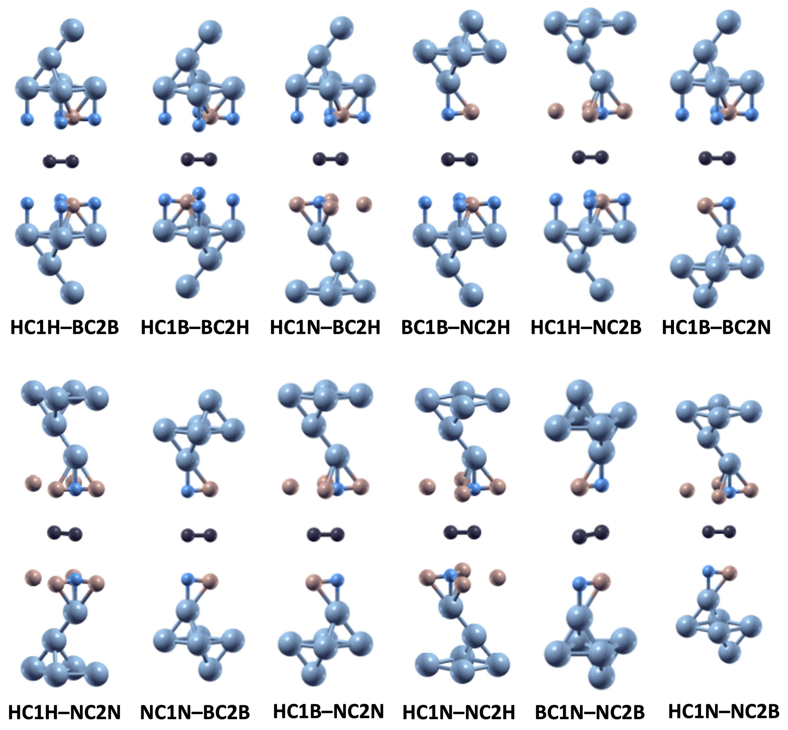
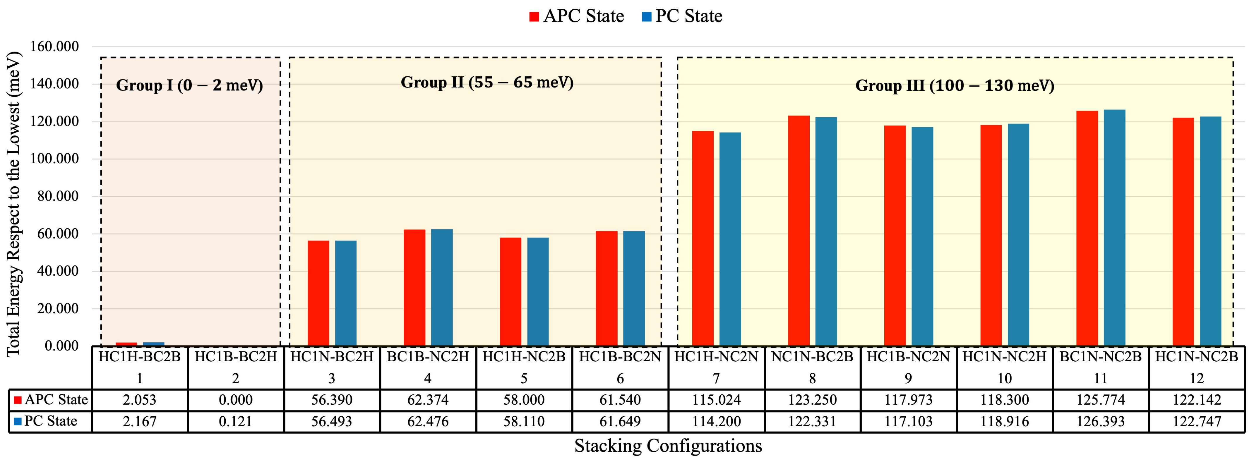
3.1. Total Energy and Its Correlation to Van Der Waals Interaction

The relative total energy (relative to the lowest total energy) of all 12 stacking configurations in the APC and PC states is shown in Figure 2. The stacking configuration with HC1B–BC2H had the lowest total energy, which means it is the most stable (ground state) configuration among the twelve stacking configurations. The 12 stacking configurations can be divided into three groups according to the relative total energy range to the lowest energy, as shown in Figure 2. Stacking configurations with a relative total energy range of 0 2 meV fall under the first category (Group I). The stacking configurations HC1H–BC2B and HC1B–BC2H fall under this category. The second category (Group II) consists of stacking configurations, such as HC1N–BC2H, BC1B–NC2H, HC1H–NC2B, and HC1B–NC2N, with a relative total energy range of 55 65 meV. Stacking configurations with a relative total energy range of 100 130 meV, such as NC1N–HC2H, NC1N–BC2B, HC1B–NC2N, HC1N–NC2H, and BC1N–NC2B, make up the third category (Group III). The three groups of stacking configurations correspond to the van der Waals interactions between the layers of hBN and graphene. The total energy difference between the most stable and other stacking configurations corresponds to the difference in van der Waals binding energy between Ni/hBN slabs and graphene. The van der Waals binding energy between Ni/hBN slabs and graphene ( E b ) at Ni/hBN–graphene–hBN/Ni junctions can be described as follows:
E b = E tot N G × E G N Ni / hBN × E Ni / hBN ,
where E tot , E G , and E Ni / hBN are the total energies per unit cell of the Ni/hBN–graphene–hBN/Ni, graphene, and Ni/hBN slabs, respectively; N G and N Ni / hBN are the quantities of graphene and Ni/hBN slabs, respectively. The total energy of Ni/hBN slabs is the same for all 12 possible stacking configurations since the same stacking configuration of hBN and Ni slabs (top-FCC) was considered. Similarly, the total energy of graphene is also the same for all stacking configurations since the graphene keeps its flat structure in all cases. Thus, the total energy difference of the Ni/hBN–graphene–hBN/Ni junction between different stacking configurations is equal to the van der Waals binding energy difference between Ni/hBN slabs and graphene:
Δ E b = Δ E tot = E tot i E tot 0 ,
where E tot i and E tot 0 are the Ni/hBN–graphene–hBN/Ni junctions’ total energies for any stacking configuration and for the most stable configuration, respectively. Therefore, Figure 2 shows that Group I (or III) has the strongest (or weakest) van der Waals binding energy between graphene and hBN/Ni slabs among all 12 possible stacking configurations.
The interlayer distance between the hBN and graphene for both the upper and lower hBN layers is shown in Table 1. According to Table 1, compared to the other groups, Group I has the smallest interlayer distance between hBN and graphene. This smallest interlayer distance corresponds to the interaction between the localized electron density of hBN’s N atoms, the Ni’s surface state, and the π -orbital of graphene. Because there is less repulsive electron screening interaction between the C atoms of graphene and the N atoms of hBN, the van der Waals bonding between hBN and graphene is strongest when N atoms are not positioned above or below the C atoms of graphene. Additionally, the relative total energy rises depending on whether N hBN atoms are positioned above or below C graphene atoms. This increase is caused by a stronger repulsive electron screening interaction, which weakens van der Waals bonding and increases the interlayer distance between the layers of hBN and graphene. This characteristic can be seen in Groups II and III. In Group II, one of the Ni/hBN slabs (lower or upper) has N atoms in line with one of the C atom sublattices (C1 or C2). The interlayer distance of the stacking configuration in this group, shown in Table 1, shows that the interlayer distance between hBN and graphene became greater than that in Group I. Furthermore, when N atoms of both the upper and lower hBN layers are in line with one or both graphene C atoms, which corresponds to Group III, the relative total energy increases even more. The greater hBN–graphene interlayer distance correlates with the rise in relative energy. This result is consistent with a prior investigation on the stacking of hBN– graphene–hBN [48]. However, in this instance, additional electron screening occurs at the interface as a result of the charge transfer from the Ni atoms at the interface to the N atoms of the hBN. By categorizing the 12 stacking configurations into three groups, it makes hBN and graphene’s electron screening repulsion stronger than it was in the earlier study.

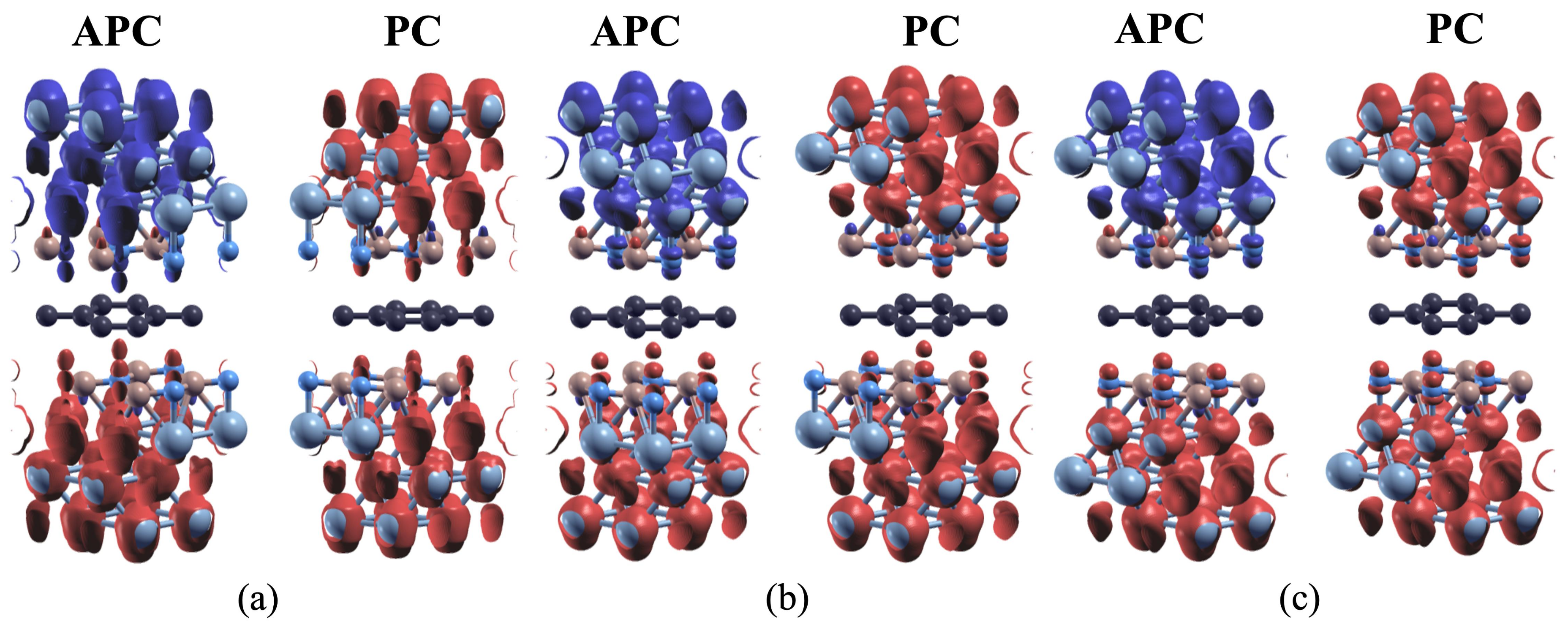
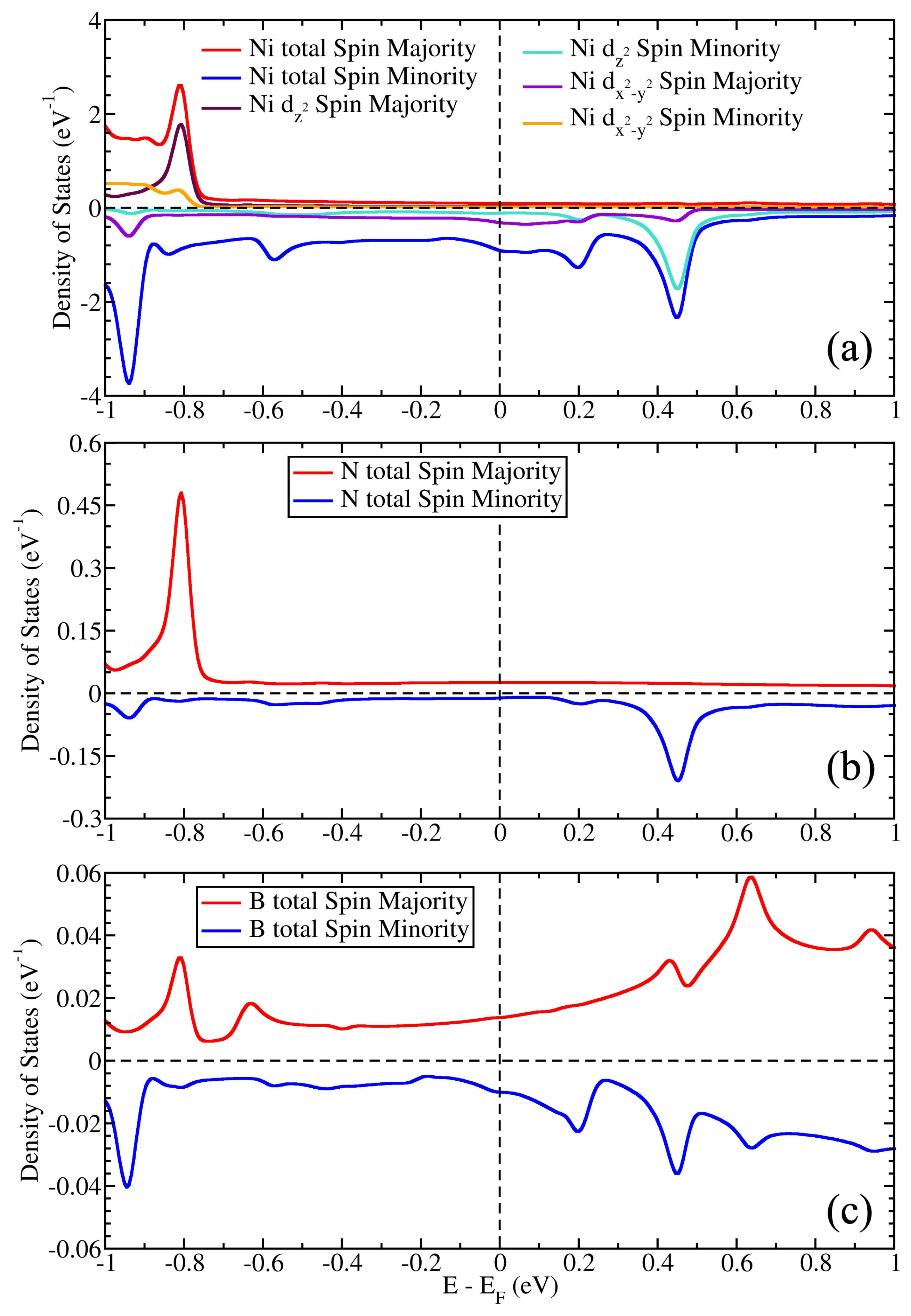
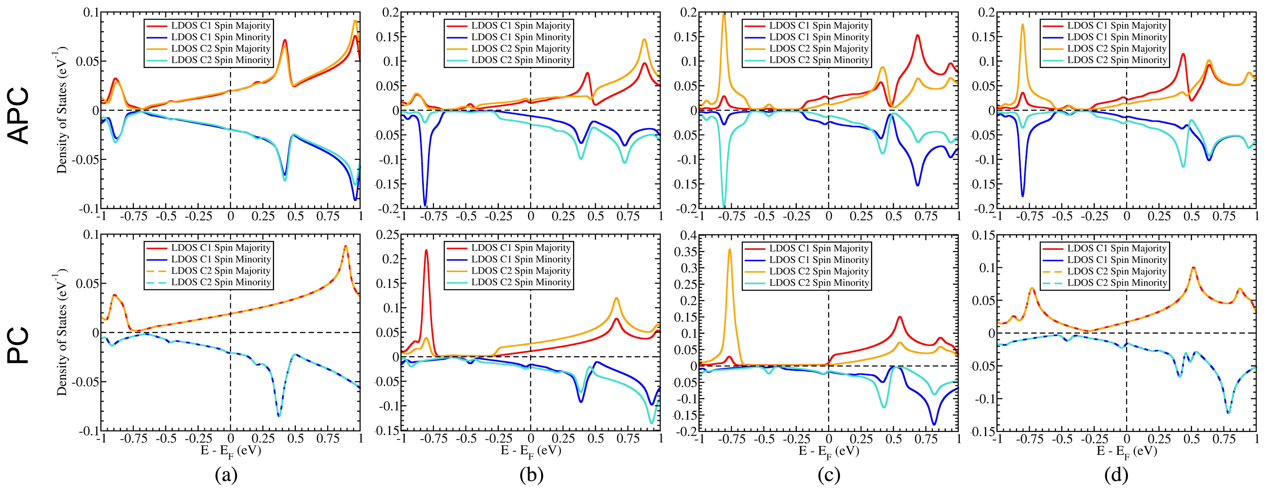
3.2. Magnetic Properties and Induced Magnetic Moments on Graphene

All 12 stacking configurations have a relatively small total energy difference between the APC and PC states, which suggests that the magnetic coupling between two Ni slabs is not very strong. Figure 3 displays the spin-charge density mapping for each group represented by BC1H–HC2B (Group I), BC1B–NC2H (Group II), and BC1N–NC2B (Group III). Induced magnetic moments on hBN layers demonstrate that the N (or B) atoms have moments in the same (or opposite) spin direction as the Ni atoms. All stacking configurations share this characteristic.
One of the Ni/hBN slabs in BC1N–NC2B is used as an example to investigate the detailed magnetic properties of Ni/hBN slabs. The Ni slab was set to have an upward magnetization direction. The LDOS of Ni and N atoms at the Ni/hBN interface shows that a strong hybridization was created between the Ni d z 2 -orbital and the N p z -orbital, based on the overlapping peak at E E F = 0.8 ( 0.44 ) eV for the spin majority (or minority) channel, as shown in Figure 4a,b. The peak also shows that the magnetic moment orientation of N atoms has the same direction as Ni slabs. In the LDOS of Ni, the spin majority channel has lower energy than the spin majority channel since the spin-up direction of magnetization was set in the calculation. Because of the DOS peak at E E F = 0.8 eV in the spin majority channel of N atoms, the N atoms have an induced magnetic moment orientation, which has a spin-up direction, as do the Ni slabs.
On the other hand, B atoms do not have strong pd-hybridization with the Ni d z 2 -orbital, based on the small DOS peak at E E F = 0.8 eV in the spin majority channel of B atoms, as shown in Figure 4c. However, B atoms have a slightly stronger hybridization with the Ni d x 2 y 2 -orbital, creating a high peak at E E F = 0.95 eV in the spin minority channel. There was a slightly higher peak at E E F = 0.95 eV in the spin minority channel than that found at E E F = 0.8 eV in the spin majority channel, resulting in B atoms with an induced magnetic moment in the spin-down direction opposite to that of the N atoms and Ni slabs. Finally, as the Ni slabs are set to have a downward magnetization direction, opposite characteristics of magnetic properties and LDOS are expected to be found in the Ni, N, and B atoms. These magnetic properties in the Ni/hBN slabs are consistent with our previous studies [27].
In the graphene case, its induced magnetic moment characteristics are not clearly shown in Figure 3. However, Table 2 shows that a small but non-negligible induced magnetic moment was observed on the graphene. Graphene has magnetic moment properties related to the Ni/hBN-graphene stacking configuration. Therefore, the total energy difference between APC and PC states might come from the induced magnetic moment configuration, which occurs on C atoms in graphene layers due to the proximity effect of Ni surface states.
The induced magnetic moment on C atoms in sublattice A (C1) and sublattice B (C2) is displayed in Table 2. Since the Ni atoms at the interface hybridized with the N atoms of hBN and the N atoms were positioned above and below the hollow site of graphene, the Ni surface state for Group I acts on the p i -orbital of graphene. This means that the spin-charge density of C atoms is not directly perturbed by the Ni surface state as an evanescent wave. When the PC state is taken into account, a small but non-negligible magnetic moment is seen on the C atoms, as shown in Table 2. This small induced magnetic moment on C atoms in Group I corresponds to the proximity effect originating from the surface state of B atoms. The LDOS of C1 and C2 atoms of graphene in the HC1B–BC2H stacking configuration (representative of Group I) shows that, in the PC state, a high DOS peak was found at E E F = 0.92 eV in the spin majority channel, as shown in Figure 5b. This peak leads to the spin-up direction of the magnetic moment for both C1 and C2 atoms. This peak corresponds to the peak found in the spin minority channel of B atoms at the same energy. The opposite magnetic moment direction between C and B atoms comes from the unique magnetic response of graphene [8,25]. The magnetic properties of the HC1H–BC2B and the HC1B–BC2H, however, are slightly different. The magnetic moment of C2 atoms in HC1H–BC2B is greater than that of C1 atoms. This outcome is caused by the fact that B atoms are positioned above and below C2 atoms and that the magnetic moment that was slightly induced on B atoms inducing a magnetic moment on C2 atoms gives 0.001 m u B higher than that of C1 atoms. Conversely, due to the fact that the upper and lower B atoms are situated beneath or above various graphene sublattices in HC1B–BC2H, an equal magnetic moment was observed.
On the other hand, in the APC state, a high DOS peak at E E F = 0.92 eV was found in both spin majority and minority channels for the HC1B–BC2H stacking configuration, as shown in Figure 5a. This is because the upper and lower Ni/hBN slabs have opposite magnetization directions, and the B atoms of the upper and lower hBN were aligned with two different graphene sublattices. Therefore, the slightly different peak height creates a small induced magnetic moment on C1 and C2 atoms with opposite spin directions. Thus, a small magnetic moment of 0.001 μ B is observed on C1 and C2 with an antiferromagnetic order. Furthermore, different behavior in the induced magnetic moment in the HC1H–BC2B stacking configuration was observed. In the HC1H–BC2B case, the induced magnetic moment, which comes from the B atoms’ proximity effect, is canceled out since both upper and lower B atoms are located above and below C2 atoms. Thus, no induced magnetic moment was observed on C1 and C2 atoms of graphene, as shown in Table 2 No. 1.
When the Group II stacking configuration is taken into account, one of the two hBN layers—either the upper or lower layer—has N atoms that have been hybridized with Ni atoms at the interface, lining up with C atoms. Here, the spin-charge density of the C atoms is directly affected by the proximity effect from one of the hBN/Ni slabs. Table 2 shows that all stacking configurations in Group II generally create a higher induced magnetic moment on graphene than in Group I. As a representative of Group II, the BC1B-NC2H stacking configuration was used to investigate the electronic state of the graphene layer. In this stacking configuration, the position of the N atoms is not symmetric, i.e., the upper N atoms are in line with C1 atoms, and the lower N atoms are in line with graphene’s hollow site. The repulsive electron screening interaction becomes stronger since the upper N atoms are in line with C1 atoms. Table 3 shows a comparison of the Mulliken partial atomic charge population for the HC1B–BC2H (Group I) and BC1B–NC2H (Group II) stacking configurations. The table shows that the charge transfer occurs within the upper hBN and graphene layers, maintaining van der Waals bonding that is more dominant than the repulsion force of the electron screening, resulting in an equilibrium state. This charge transfer mechanism determines the induced magnetic properties found on the graphene layer. In the PC state being considered, the LDOS of graphene shows that a high peak DOS was observed on C1 atoms in the spin majority channel, as shown in Figure 5b. This peak is created because charge transfer occurred from C1 to C2 atoms within the graphene layer and from N to B atoms within the upper hBN, as shown in Table 3. Due to the charge transfer from N to B atoms within the upper hBN, the high DOS peak of B atoms LDOS in Figure 4c at E E F = 0.92 eV is expected to become higher, thus yielding a greater proximity effect on C1 atoms. Additionally, the charge transfer occurs from C2 to C1 atoms within graphene. It makes the DOS peak of C1 atoms at E E F = 0.92 eV in the spin majority channel much higher, as shown in Figure 5b. This high peak leads to the spin-up direction of the magnetic moment on C1 atoms. The oppositely induced magnetic moment of C2 atoms comes from the half-filled p z -orbital, and Pauli exclusion principles are often found in organic molecules in s p 2 hybridization or the magnetic alternant hydrocarbon system [49]. A similar case was also found when the APC state was considered. However, since the upper Ni/hBN slab has a downward magnetic moment orientation, the high DOS peak of C1 atoms was in the spin minority channel, leading to the spin-down direction of the induced magnetic moment.
The position of the N atoms in the upper and lower hBN, or whether they are symmetric or asymmetric, determines the magnetic moment that is induced on graphene for the stacking configuration in Group III. The N atoms of the hBN layers were positioned above and below the C atoms in Group III. Therefore, it is said to be symmetric when one of the graphene sublattices of the C atoms lines up with one of the N atoms of the upper and lower hBN layers. When the N atoms in the upper and lower hBN layers align with different C atom sublattices, such as the upper hBN with C1 and the lower hBN with C2, this is referred to as being asymmetric. When compared to other stacking configurations, Group III symmetric stacking configurations showed the greatest induced magnetic moment on graphene when the PC state was taken into account. The charge transfer mechanism within hBN and graphene becomes more significant since both upper and lower N atoms are in line with one C atom’s sublattice. Figure 5c shows a high DOS peak at E E F = 0.92 eV on C2 atoms for the spin majority channel in the NC1N–BC2B stacking configuration while a PC state is considered. This high DOS had the highest intensity compared to the high DOS found at the same energy in Groups I and II. This causes C2 atoms to have a spin-up magnetic moment with the largest amplitude compared to Groups I and II. Similar to Group II, due to the AFM interaction between C1 and C2 atoms, C1 atoms have an induced magnetic moment in a spin-down direction with almost the same value as that found in C2 atoms. However, when the APC state was considered, a high DOS peak was created in both the spin minority and minority channel of C2 atoms, resulting in no induced magnetic moment on graphene. The induced magnetic moment of graphene in the APC state is also significant when taking into account asymmetric stacking configurations. This property results from the proximity effect, which affects the C1 and C2 graphene atoms equally. Since graphene prefers to have an antiferromagnetic order and the upper and lower Ni slabs have opposite directions, the induced magnetic moments of the C1 and C2 atoms reinforce one another. The proximity effect, however, produces a ferromagnetic order on the magnetic moments of C1 and C2 atoms when the system is in a PC state. The effect is diminished as a result of the antiferromagnetic properties of the C atoms in graphene, so the value is only marginally significant.

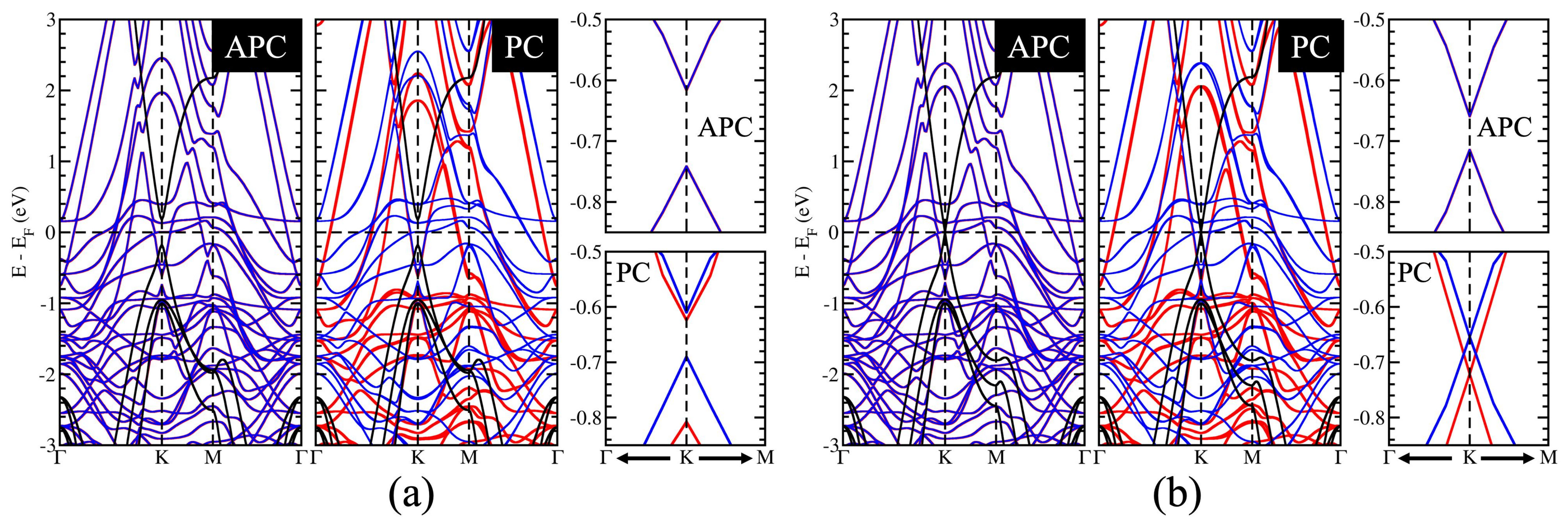
3.3. A Controllable Dirac Cone of Graphene due to a Tunable Pseudospin Term of Graphene

From the effective-mass Hamiltonian picture, the Dirac cone of graphene occurs due to the perseverance of the chiral symmetry of graphene, having equipotential between C1 and C2 [50]. Thus, the chiral symmetry is broken when a potential difference is created between C1 and C2, creating an MGDC with a gap size proportional to the potential difference between C1 and C2 [51]. In the case of the hBN–Gr–hBN heterostructure, the MGDC of graphene is open or closed depending on the stacking configuration [48]. The electron screening repulsion between hBN and graphene becomes the main determinant of whether the stacking configuration results in an open or closed MGDC. However, in the Ni/hBN–Gr–hBN/Ni heterostructure, the potential difference in the graphene sublattice could come from 1. the electron screening repulsion between hBN and graphene layers, 2. the Ni’s surface state, and/or 3. the induced magnetic moment on graphene. Thus, different characteristics of the Dirac cone might be found when two different magnetic alignments, the APC and PC states, are considered.
In the DFT spin-GGA calculations, the effective potential has a contribution approximately proportional to the spin-charge density:
V e f f σ ( r ) = n ( r ) | r r | d r + δ E X C G G A [ n ( r ) , n ( r ) ] δ n σ ( r ) + V e x t ( r ) + μ B ( r ) .
Thus, the spin-charge density characteristics of C1 and C2 correlate to the properties of the graphene’s Dirac cone. Table 4 introduced the integrated spin-charge density n η , σ of the C atom p z -orbital, where η is either C1 or C2, and σ is either spin-up (↑) or spin-down (↓). The value of n η , σ corresponds to the population of the partial charge of the atom (both for spin-up and spin-down electrons) and is assumed to be determined by integrating n σ ( r ) within an ionic radius of the atom. The special p z -orbital was chosen due to its correlation with the π -orbital of graphene.
For the stacking configurations in Group I, both HC1H–BC2B and HC1B–BC2H have N atoms above and below the hollow site of the graphene layer. However, the location of the B atoms is different. The B atoms in HC1H–BC2B (HC1B–BC2H) are symmetrically (asymmetrically) positioned. The different arrangement of the upper and lower B atoms of hBN leads to different potential characteristics for C1 and C2. Thus, HC1H–BC2B and HC1B–BC2H are expected to show differences in the properties of graphene’s Dirac cone.
In HC1H–BC2B, since both the upper and lower B atoms of hBN align with C2 atoms, a modulated potential that comes from the electron screening repulsion between hBN and graphene layers is expected. However, the different induced magnetic characteristics of graphene between the APC and PC states lead to different modulations of potential. Table 4 No. 1 shows that the spin-charge density of C1 and C2 in the APC state can be described by using the following equation:
n C 2 , = n C 2 , > n C 1 , = n C 1 , .
The electron screening repulsion between the C2 and B atoms causes the difference between n C 2 , σ and n C 1 , σ to exist. The spin-charge density between C1 and C2 atoms is modulated based on Equation (4). Thus, there is also a modulation of the effective potential between C1 and C2 atoms. Figure 6a depicts the open-gapped Dirac cone produced by this modulation. However, due to the absence of an induced magnetic moment on graphene, the band structure of spin majority and spin minority channels overlaps because the difference in spin-charge density between spin-up and spin-down electrons is the same. However, when the PC state is taken into account,
n C 2 , > n C 2 , > n C 1 , > n C 1 , .
This demonstrates that C1 and C2 atoms had an induced magnetic moment. Figure 6a depicts a gapped Dirac cone that is open and spin-polarized. Equation (5) states that the open and spin-polarized Dirac cone comes from the potential difference between C1 and C2 atoms, which are modulated and spin-polarized. Compared with the hBN–Gr–hBN system, shown by the solid black curve in Figure 6a, the potential modulation created from the induced magnetic moment of graphene only creates a difference in whether the MGDC becomes spin-polarized or not when either the APC or PC state is considered.
However, a different result was found when HC1B–BC2H was considered. The electron screening repulsion between B and C atoms occurs on C1 and C2 atoms in the case of HC1B—BC2H in the APC state. The magnetic moment on the C atoms, which was induced by the magnetic moment on the B atoms, as shown in Table 4 No. 2 results in modulated spin-charge density:
n C 1 , = n C 2 , > n C 1 , = n C 2 , .
Equation (6) demonstrates that the potentials between C1 and C2 atoms are modulated and that there is no difference in the spin-charge densities of spin-up or spin-down electrons. Therefore, as shown in Figure 6b, the gapped Dirac cone is open with spin majority and minority channel overlap. However, in the PC state, HC1–BC2H exhibits a closed Dirac cone. This property results from the asymmetric positioning of the B atoms, which produced an equivalent spin-charge density between C1 and C2 by inducing the same magnetic moment on the C atoms:
n C 1 , = n C 2 , > n C 1 , = n C 2 , .
Thus, it was predicted that the equipotential would maintain chiral symmetry and produce a closed-gapped Dirac cone. Additionally, the closed Dirac cone becomes polarized due to the spin-charge density between spin-up and spin-down electrons, as demonstrated in Figure 6b.
The importance of the induced magnetic contribution in determining the opening or closing of the MGDC can be observed by making a comparison with the graphene Dirac cone of the hBN–Gr–hBN system in the HC1B–BC2H stacking configuration, shown by the solid black curve in Figure 6b. In the case of the hBN–Gr–hBN system, the contribution of the electron screening repulsion interaction between B atoms of upper (or lower) hBN and C2 (or C1) atoms of graphene creates an equipotential between C1 and C2. Thus, the chiral symmetry is preserved, and the Dirac cone of graphene is closed. Therefore, by introducing the potential modulation created from the induced magnetic moment of graphene, a controllable MGDC of graphene becomes possible.
Finally, it was shown that HC1B–BC2H has a property where the MGDC of graphene can be controlled, i.e., it can open and close depending on the magnetic alignment of the upper and lower Ni slabs. This controllable MGDC property comes from the controllable induced magnetic moment of graphene. However, the gap of the Dirac cone, which was shown in the APC state, is relatively small. This small gap is due to the influence of weak hybridization between Ni and C atoms via a damped Ni d z 2 surface state and C p z . In the following section, a scheme for controlling the gap size in the APC state will be introduced.

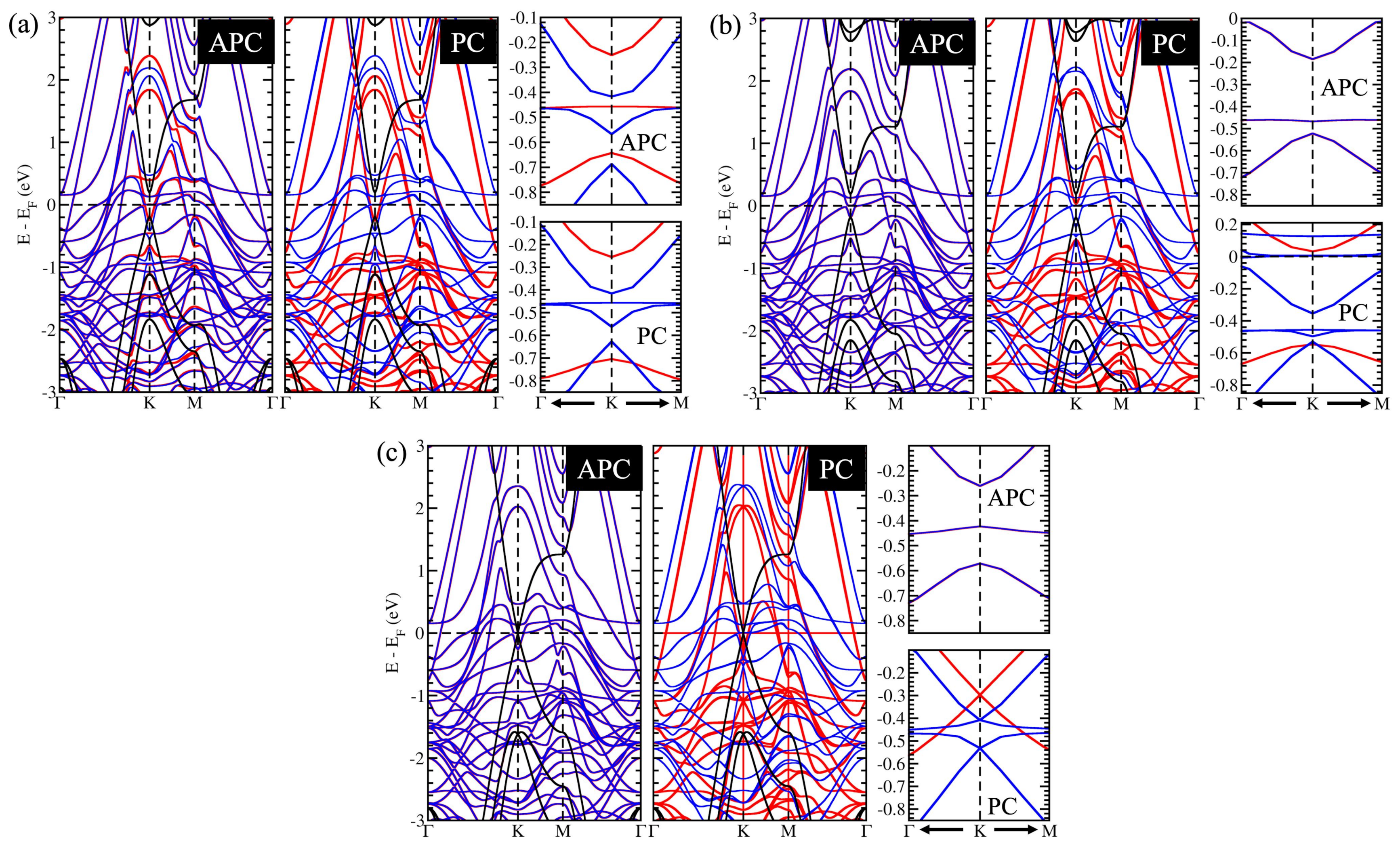
3.4. The Influence of the Surface State of Ni Works Directly on C Atoms in the Gapped Dirac Cone

As shown in Table 2 Nos. 3, 4, 5, and 6, a different induced magnetic moment with a different orientation was observed between C1 and C2 when the N atoms of one of the hBN layers, upper or lower, are in the APC or PC state. Due to the substantial difference in spin-charge density between C1 and C2, modulation of potential was therefore anticipated for C1 and C2 atoms. The HC1N–BC2H stacking configuration case, displayed in Table 4, serves as one example. This modulation causes an MGDC of graphene to be visible in Figure 7a for both APC and PC state cases. However, it is interesting to note that there is a sizable difference in the gap size between the spin majority and spin minority channels. For instance, in both APC and PC cases, the bandgap of the spin majority channel is greater than 200 meV, while the bandgap of the spin minority channel is lower than 100 meV. The integrated spin-charge density can account for this characteristic. When the APC state is taken into account, the spin-charge density difference between spin-up and spin-down electrons is nearly three times greater. Therefore, compared to the spin minority channel, the MGDC is more noticeable there. When the PC state was taken into account, this notable difference was also discovered.
The direct perturbation of the Ni surface states on C1 atoms is the cause of the significant difference in spin-up electrons. The magnetic moment is spinning up in the lower Ni slab. Because graphene prefers to have an antiferromagnetic order with the magnetic moment direction of Ni slabs, the C1 has an induced magnetic moment in a spin-down direction. Because the spin-up electron density is suppressed and consequently lower than the spin-down electron density, C1 and C2 have significantly different spin-up electron densities. From these results, it is suggested that the MGDC of graphene can be significantly increased, resulting in a sizeable gap, by creating a stacking configuration where the Ni surface states directly affect one of the graphene C atom sublattices.

3.5. Controllable Mass-Gapped Dirac Cone through the Ni Surface State Influence on C Atoms

In Group III, the C atoms’ spin-charge density of graphene gets a direct perturbation from Ni atoms at the interface of both the upper and lower Ni slab surface states. In this case, the proximity effect of the upper and lower Ni slabs on the C atom can be divided into two types: symmetrical and asymmetrical, in which the surface state affects one C atom sublattice and two different C atom sublattices, respectively. Conversely, HC1N–NC2H, BC1N–NC2B, and HC1N–NC2B are asymmetric, while NC1N–HC2H, NC1N–BC2B, and HC1B–NC2N are symmetric. The graphene’s spin-charge density is affected differently by symmetric and asymmetric structures, leading to different MGDC behavior.
In the symmetric case, such as the HC1H–NC2N, graphene does not have an induced magnetic moment in the APC state, but it does in the PC state, where it has a larger induced magnetic moment than Group II. However, even though the graphene’s induced magnetic moment is shown as zero in the APC state (Table 2 No. 7), Figure 7b depicts the MGDC in the spin majority and minority channels. Table 4 No. 4 can be used to explain this. Although the magnetic proximity effect is negated on graphene, the surface state of Ni directly perturbs the spin-charge density of the C2 atoms, leading to different spin-charge density mapping between C1 and C2. Nevertheless, the spin-up and spin-down electron density differences are the same because the upper and lower stacking configurations are symmetric, which causes the MGDC to overlap on the spin majority and minority channels.
The induced magnetic moments in C1 and C2 are distinct in the case of the PC state. Thus, the spin-charge densities of spin-up and spin-down electrons differ significantly. The stacking configuration of NC1N–HC2H demonstrates this. It demonstrates that there is a clear difference in the spin-down electron densities between C1 and C2. The spin-up electron density, on the other hand, revealed a minimal electron density difference between C1 and C2. The magnetic response of C1 atoms, which frequently have an antiferromagnetic order with Ni atoms, is what gives this property. As a result, the spin-down charge density of the C1 atoms increases relative to the spin-up charge density, whereas the spin-down electron of the C2 atoms decreases. Therefore, as shown in Figure 7a, the MGDC for the spin majority channel is slightly open. Meanwhile, the MGDC in the spin minority channel is open and significantly larger than it is in Group II. All of the stacking configurations in Group III, which is under the symmetric perturbation of the proximity effect, exhibit this characteristic.
However, for the proximity effect that gives an asymmetric perturbation, a similar characteristic to that found in our prior study was noted [25]. The stacking configuration of BC1N–NC2B served as one example. The Ni atoms at the interface of the upper and lower Ni slabs’ surface states perturb two different graphene sublattices, i.e., lower Ni on C1 and upper Ni on C2. As a result, when the APC state is taken into account, distinct induced magnetic moments on C1 and C2 are noticed. Figure 7c depicts the open MGDC on graphene for both spin majority and minority channels as a result of the chiral symmetry breaking caused by this difference. This situation is somewhat similar to that in the HC1B–BC2H stacking configuration, but the proximity effect is more pronounced because it directly perturbs C atoms. It can be seen from Table 4 No. 5 that the spin-charge density difference is significantly larger than it was for HC1B–BC2H. It is interesting to note that the gap size is similar to that of Ni/graphene/Ni MJs, as reported in our previous study [25]. Last but not least, the induced magnetic moment on C1 and C2 in the PC state has the same strength and direction. As a result, the Dirac cone is preserved and spin-polarized, as shown in Figure 7c.

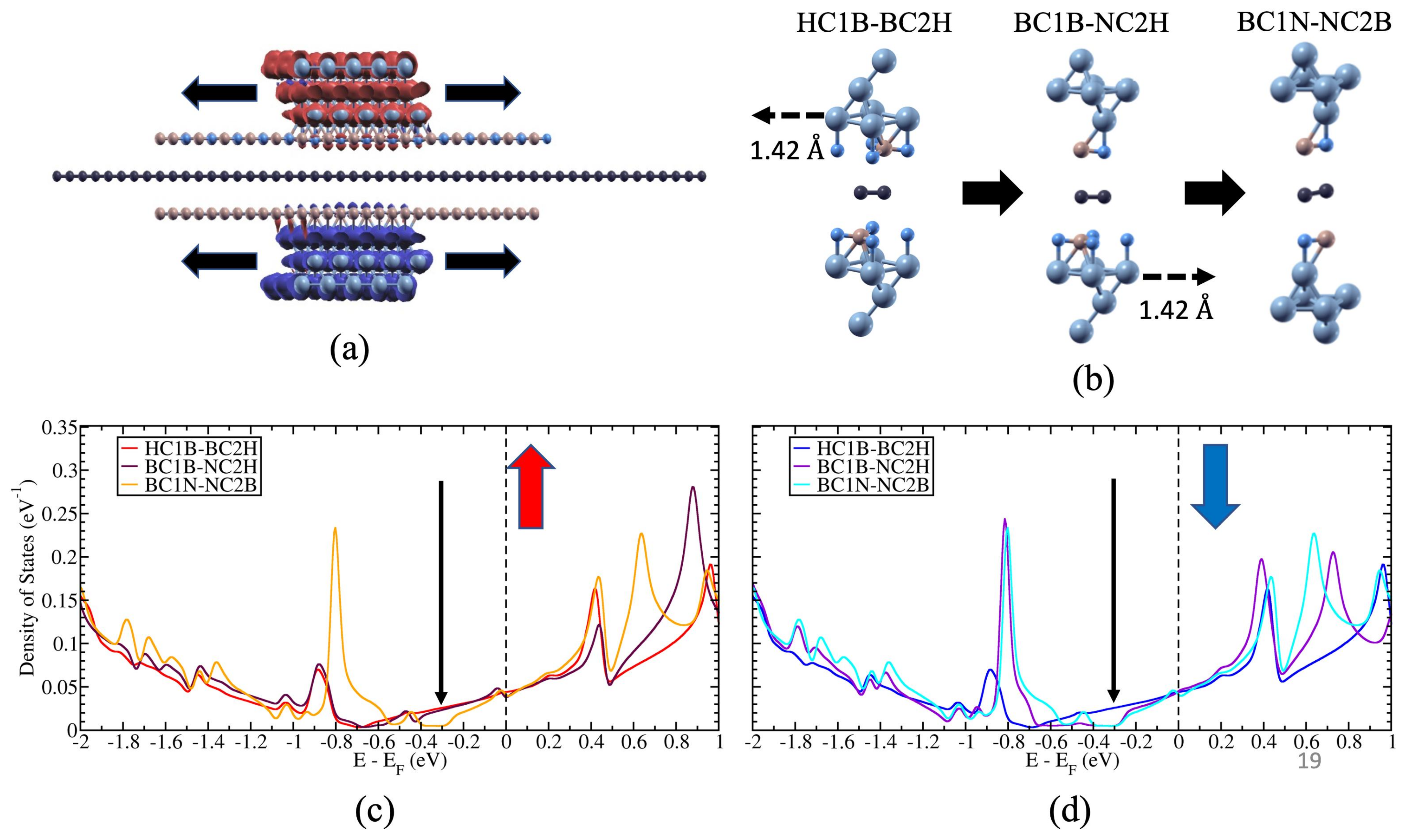
3.6. Possible Application on the Spin-Topological Electronic Valve

The controllable MGDC of graphene in Ni/hBN–Gr–hBN/Ni, which depends on the stacking configuration, can be proposed as a device where a controllable MGDC is tuned using mechanical motion. This is because the van der Waals interaction between hBN and graphene is weak enough for the hBN to be mechanically translated to create another stacking configuration. Recently, tilting the overlapping of the hBN–Gr–hBN structure to have a particular angle and creating a Moire pattern is experimentally possible [52]; thus, a translation motion can also be expected. Additionally, since the van der Waals bonding difference between each group configuration is so small, in the range of 50–70 meV, where it is in the order of 10 21 Nm, it is reasonable to have translation motion between two different configurations of two different groups. Thus, by taking into account the APC state on Ni/hBN–Gr–hBN/Ni with the device structure shown in Figure 8a, such a device can be suggested. The upper slab of Ni/hBN can be moved translationally by a shift of 1.42 Å to create the most stable stacking configuration; HC1B–BC2H becomes BC1B–NC2H. To achieve a BC1N–NC2B stacking configuration from the BC1B–NC2H, the lower Ni/hBN slab can be moved translationally by a shift of 1.42 Å. Figure 8b depicts this proposed shifting process. Since the LDOS of graphene corresponds to its in-plane conductance [26], the LDOS shown in Figure 8c for spin-up and (d) for spin-down implies three different in-plane conductance states for each proposed stacking configuration. Only the BC1N–NC2B stacking configuration showed an MGDC at E E F = 0.3 eV for spin-up electrons. On the other hand, BC1B–NC2H and BC1N–NC2B both exhibit MGDC for spin-down electrons. There is no MGDC in only HC1B–BC2H. The in-plane conductance difference ratio between the two structures is shown in Table 5. Finally, three different non-volatile memory states can occur by changing the stacking configuration from HC1B–BC2H to BC1N–NC2B.

4. Conclusions

In this study, we proposed a spin-topological electronic valve in a Ni/hBN–graphene–hBN/Ni magnetic junction to control the in-plane conductance of graphene. The spin-topological electronic valve can be realized by controlling the topological nature of graphene’s MGDC through the magnetic proximity effect. The first-principles investigation was conducted to show how the mechanism of graphene’s MGDC is controlled. Twelve stacking configurations were proposed, with two magnetic configurations on upper and lower Ni slabs, APC and PC. The 12 stacking arrangements were divided into three groups based on their relative total energy. Group I included configurations with a total energy range of 0–2 meV, with HC1B–BC2H and HC1H–BC2B having the lowest total energy. Group II included configurations with a total energy range of 55–65 meV, such as HC1N–BC2H, BC1B–NC2H, HC1H–NC2B, and HC1B–NC2N. Group III consisted of stacking configurations with relative total energies between 100 and 130 meV. The study found that the properties of graphene’s MGDC in Group I depended on the arrangement of the upper and lower B atoms. When the arrangement of B atoms is asymmetric, the MGDC is able to open and close in APC and PC states, respectively. On the other hand, when the arrangement of B atoms is symmetric, the MGDC remains open for both APC and PC states. Nevertheless, a relatively small gap in the MGDC was observed in Group I. In Group II, the Ni surface state directly affected the MGDC of graphene, resulting in a wider gap of MGDC in the spin majority channel. However, since only one part of the Ni surface state, either from the upper or lower slab, affected one of the graphene sublattices, both APC and PC states resulted in an open MGDC. In Group III, the upper and lower Ni slab surface states affected both C atoms on the sublattices of graphene. In the APC state, a noticeable mass gap was observed for both asymmetric and symmetric cases, with the spin majority and minority channels overlapping. On the other hand, when the PC state is considered, a symmetric arrangement shows one of the spin channels has a larger mass gap than in Group II, while another spin channel has a relatively smaller mass gap. However, the chiral symmetry is preserved in the PC state in the asymmetric case, producing a spin-polarized Dirac cone. By utilizing the unique properties of graphene’s MGDC in the Ni/hBN–graphene–hBN/Ni magnetic junction, which depend on the stacking configuration, a controllable MGDC using mechanical motion can be proposed by suggesting a device that can translate the top and bottom Ni(111)/hBN slabs. This can be realized by considering an APC state on Ni/hBN–Gr–hBN/Ni and changing its configuration from HC1B–BC2H to BC1B–NC2H followed by BC1B–NC2H to BC1N–NC2B. Three different in-plane conductances of graphene were observed, corresponding to three non-volatile memory states. This device provides insight into MJs having three or more non-volatile memory states that cannot be found in conventional MJs.

Supplementary Materials

The following supporting information can be downloaded at: https://www.mdpi.com/article/10.3390/magnetochemistry9050113/s1.

Author Contributions

Conceptualization was performed by Y.W., K.K., H.H. and G.K.S. performed computer simulations of the atomic layered systems, and M.A.M. conducted the theory of atomic layered materials. Y.W. determined the equilibrium structure of the proposed system and determined spin-charge density mapping, band structures, and local density of states (LDOS) of the proposed system. All authors wrote the original draft of the manuscript. All the authors have reviewed the manuscript. The manuscript was written through the contributions of all authors. All authors approved the final version of the manuscript.

Funding

This study was partly supported by the Japan Society for the Promotion of Science (JSPS) KAKENHI (Grant No. JP19H00862 and JP16H00914 in the Science of Atomic Layers, 21J22520 and 20J22909 in the Grant-in-Aid for Young Scientists, and JP18K03456).

Institutional Review Board Statement

Not applicable.

Informed Consent Statement

Not applicable.

Data Availability Statement

The data presented in this study are contained within the article and Supplementary Information file.

Acknowledgments

Calculations were performed at the computer center of Kyushu University. Y.W. and H.H. gratefully acknowledge the fellowship support from the JSPS. In addition, G.K.S. and M.A.M. acknowledge the JSPS Invitational Fellowships (Grant No. L21547 and S21113, respectively).

Conflicts of Interest

There are no conflict of interest to declare.

References

  1. Geim, A.K.; Novoselov, K.S. The rise of graphene. Nat. Mater. 2007, 6, 183–191. [Google Scholar] [CrossRef] [PubMed]
  2. Novoselov, K.S.; Geim, A.K.; Morozov, S.V.; Jiang, D.; Katsnelson, M.I.; Grigorieva, I.V.; Dubonos, S.V.; Firsov, A.A. Two-dimensional gas of massless Dirac fermions in graphene. Nature 2005, 438, 197–200. [Google Scholar] [CrossRef] [PubMed]
  3. Morozov, S.V.; Novoselov, K.S.; Katsnelson, M.I.; Schedin, F.; Elias, D.C.; Jaszczak, J.A.; Geim, A.K. Giant Intrinsic Carrier Mobilities in Graphene and Its Bilayer. Phys. Rev. Lett. 2008, 100, 016602. [Google Scholar] [CrossRef]
  4. Schedin, F.; Geim, A.K.; Morozov, S.V.; Hill, E.W.; Blake, P.; Katsnelson, M.I.; Novoselov, K.S. Detection of individual gas molecules adsorbed on graphene. Nat. Mater. 2007, 6, 652–655. [Google Scholar] [CrossRef]
  5. Schultz, B.J.; Jaye, C.; Lysaght, P.S.; Fischer, D.A.; Prendergast, D.; Banerjee, S. On chemical bonding and electronic structure of graphene–metal contacts. Chem. Sci. 2013, 4, 494–502. [Google Scholar] [CrossRef]
  6. Abtew, T.; Shih, B.C.; Banerjee, S.; Zhang, P. Graphene–ferromagnet interfaces: Hybridization, magnetization and charge transfer. Nanoscale 2013, 5, 1902–1909. [Google Scholar] [CrossRef] [PubMed]
  7. Weser, M.; Rehder, Y.; Horn, K.; Sicot, M.; Fonin, M.; Preobrajenski, A.B.; Voloshina, E.N.; Goering, E.; Dedkov, Y.S. Induced magnetism of carbon atoms at the graphene/Ni(111) interface. Appl. Phys. Lett. 2010, 96, 012504. [Google Scholar] [CrossRef]
  8. Joshi, N.; Ballav, N.; Ghosh, P. Hydrogen-induced reversal of spin alignment in graphene supported on Ni(111) surface. Phys. Rev. B 2012, 86, 121411. [Google Scholar] [CrossRef]
  9. Novoselov, K.S.; Geim, A.K.; Morozov, S.V.; Jiang, D.; Zhang, Y.; Dubonos, S.V.; Grigorieva, I.V.; Firsov, A.A. Electric Field Effect in Atomically Thin Carbon Films. Science 2004, 306, 666–669. [Google Scholar] [CrossRef]
  10. Morishita, N.; Sunnardianto, G.K.; Miyao, S.; Kusakabe, K. Theoretical Analysis of Pseudodegenerate Zero-Energy Modes in Vacancy-Centered Hexagonal Armchair Nanographene. J. Phys. Soc. Jpn. 2016, 85, 084703. [Google Scholar] [CrossRef]
  11. Dahal, A.; Batzill, M. Graphene–nickel interfaces: A review. Nanoscale 2014, 6, 2548–2562. [Google Scholar] [CrossRef] [PubMed]
  12. Cho, Y.; Choi, Y.C.; Kim, K.S. Graphene Spin-Valve Device Grown Epitaxially on the Ni(111) Substrate: A First Principles Study. J. Phys. Chem. C 2011, 115, 6019–6023. [Google Scholar] [CrossRef]
  13. Sato, R.; Hiraiwa, T.; Inoue, J.; Honda, S.; Itoh, H. Magnetoresistance in fcc Ni/graphene/fcc Ni(111) junctions. Phys. Rev. B 2012, 85, 094420. [Google Scholar] [CrossRef]
  14. Liu, H.; Kondo, H.; Ohno, T. Spintronic Transport in Armchair Graphene Nanoribbon with Ferromagnetic Electrodes: Half-Metallic Properties. Nanoscale Res. Lett. 2016, 11, 456. [Google Scholar] [CrossRef]
  15. Martin, M.B.; Dlubak, B.; Weatherup, R.S.; Piquemal-Banci, M.; Yang, H.; Blume, R.; Schloegl, R.; Collin, S.; Petroff, F.; Hofmann, S.; et al. Protecting nickel with graphene spin-filtering membranes: A single layer is enough. Appl. Phys. Lett. 2015, 107, 012408. [Google Scholar] [CrossRef]
  16. Asshoff, P.U.; Sambricio, J.L.; Rooney, A.P.; Slizovskiy, S.; Mishchenko, A.; Rakowski, A.M.; Hill, E.W.; Geim, A.K.; Haigh, S.J.; Fal’ko, V.I.; et al. Magnetoresistance of vertical Co-graphene-NiFe junctions controlled by charge transfer and proximity-induced spin splitting in graphene. 2D Mater. 2017, 4, 031004. [Google Scholar] [CrossRef]
  17. Entani, S.; Seki, T.; Sakuraba, Y.; Yamamoto, T.; Takahashi, S.; Naramoto, H.; Takanashi, K.; Sakai, S. Magnetoresistance effect in Fe20Ni80/graphene/Fe20Ni80 vertical spin valves. Appl. Phys. Lett. 2016, 109, 082406. [Google Scholar] [CrossRef]
  18. Mohiuddin, T.M.G.; Hill, E.; Elias, D.; Zhukov, A.; Novoselov, K.; Geim, A. Graphene in Multilayered CPP Spin Valves. IEEE Trans. Magn. 2008, 44, 2624–2627. [Google Scholar] [CrossRef]
  19. Iqbal, M.Z.; Iqbal, M.W.; Lee, J.H.; Kim, Y.S.; Chun, S.H.; Eom, J. Spin valve effect of NiFe/graphene/NiFe junctions. Nano Res. 2013, 6, 373–380. [Google Scholar] [CrossRef]
  20. Iqbal, M.Z.; Iqbal, M.W.; Jin, X.; Hwang, C.; Eom, J. Interlayer dependent polarity of magnetoresistance in graphene spin valves. J. Mater. Chem. C 2015, 3, 298–302. [Google Scholar] [CrossRef]
  21. Chen, J.J.; Meng, J.; Zhou, Y.B.; Wu, H.C.; Bie, Y.Q.; Liao, Z.M.; Yu, D.P. Layer-by-layer assembly of vertically conducting graphene devices. Nat. Commun. 2013, 4, 1921. [Google Scholar] [CrossRef] [PubMed]
  22. Li, F.; Li, T.; Guo, X. Vertical Graphene Spin Valves Based on La2/3Sr1/3MnO3 Electrodes. ACS Appl. Mater. Interfaces 2014, 6, 1187–1192. [Google Scholar] [CrossRef] [PubMed]
  23. Li, W.; Xue, L.; Abruña, H.D.; Ralph, D.C. Magnetic tunnel junctions with single-layer-graphene tunnel barriers. Phys. Rev. B 2014, 89, 184418. [Google Scholar] [CrossRef]
  24. Mandal, S.; Saha, S.K. Ni/graphene/Ni nanostructures for spintronic applications. Nanoscale 2012, 4, 986–990. [Google Scholar] [CrossRef]
  25. Wicaksono, Y.; Teranishi, S.; Nishiguchi, K.; Kusakabe, K. Tunable induced magnetic moment and in-plane conductance of graphene in Ni/graphene/Ni nano-spin-valve-like structure: A first principles study. Carbon 2019, 143, 828–836. [Google Scholar] [CrossRef]
  26. Wicaksono, Y.; Harfah, H.; Sunnardianto, G.K.; Majidi, M.A.; Kusakabe, K. Colossal in-plane magnetoresistance ratio of graphene sandwiched with Ni nanostructures. RSC Adv. 2022, 12, 13985–13991. [Google Scholar] [CrossRef]
  27. Harfah, H.; Wicaksono, Y.; Sunnardianto, G.K.; Majidi, M.A.; Kusakabe, K. High magnetoresistance of a hexagonal boron nitride–graphene heterostructure-based MTJ through excited-electron transmission. Nanoscale Adv. 2022, 4, 117–124. [Google Scholar] [CrossRef]
  28. Pezo, A.; Zanolli, Z.; Wittemeier, N.; Ordejón, P.; Fazzio, A.; Roche, S.; Garcia, J.H. Manipulation of spin transport in graphene/transition metal dichalcogenide heterobilayers upon twisting. 2D Mater. 2021, 9, 015008. [Google Scholar] [CrossRef]
  29. Zollner, K.; Fabian, J. Engineering Proximity Exchange by Twisting: Reversal of Ferromagnetic and Emergence of Antiferromagnetic Dirac Bands in Graphene/Cr2Ge2Te6. Phys. Rev. Lett. 2022, 128, 106401. [Google Scholar] [CrossRef]
  30. Eliseev, E.A.; Morozovska, A.N.; Strikha, M.V. Strain Engineering of Ferromagnetic-Graphene-Ferroelectric Nanostructures. Phys. Rev. Appl. 2020, 14, 024081. [Google Scholar] [CrossRef]
  31. Harfah, H.; Wicaksono, Y.; Majidi, M.A.; Kusakabe, K. Spin-Current Control by Induced Electric Polarization Reversal in Ni/hBN/Ni: A Cross-Correlation Material. ACS Appl. Electron. Mater. 2020, 2, 1689–1699. [Google Scholar] [CrossRef]
  32. Wicaksono, Y. Theoretical Study of Gap Opening/Closing Control of Dirac Cone Using Spin-dependent Potentials in Graphene-based Magnetic Junctions. Ph.D. Thesis, Osaka University, Osaka, Japan, 2022. Available online: https://ir.library.osaka-u.ac.jp/repo/ouka/all/89505/32918_Dissertation.pdf (accessed on 21 March 2023).
  33. Sánchez-Portal, D.; Ordejón, P.; Artacho, E.; Soler, J.M. Density-functional method for very large systems with LCAO basis sets. Int. J. Quantum Chem. 1997, 65, 453–461. [Google Scholar] [CrossRef]
  34. Soler, J.M.; Artacho, E.; Gale, J.D.; García, A.; Junquera, J.; Ordejón, P.; Sánchez-Portal, D. The SIESTA method for ab initio order-N materials simulation. J. Physics: Condens. Matter 2002, 14, 2745–2779. [Google Scholar] [CrossRef]
  35. Troullier, N.; Martins, J. Efficient pseudopotentials for plane-wave calculations. Phys. Rev. B 1991, 43, 1993–2006. [Google Scholar] [CrossRef] [PubMed]
  36. Perdew, J.P.; Ruzsinszky, A.; Csonka, G.I.; Vydrov, O.A.; Scuseria, G.E.; Constantin, L.A.; Zhou, X.; Burke, K. Restoring the Density-Gradient Expansion for Exchange in Solids and Surfaces. Phys. Rev. Lett. 2008, 100, 136406. [Google Scholar] [CrossRef]
  37. Ozaki, T.; Kino, H. Numerical atomic basis orbitals from H to Kr. Phys. Rev. B 2004, 69, 195113. [Google Scholar] [CrossRef]
  38. Ozaki, T. Variationally optimized atomic orbitals for large-scale electronic structures. Phys. Rev. B 2003, 67, 155108. [Google Scholar] [CrossRef]
  39. Sánchez-Portal, D.; Artacho, E.; Soler, J. Analysis of atomic orbital basis sets from the projection of plane-wave results. J. Phys. Condens. Matter 1996, 8, 3859–3880. [Google Scholar] [CrossRef]
  40. Grimme, S. Semiempirical GGA-type density functional constructed with a long-range dispersion correction. J. Comput. Chem. 2006, 27, 1787–1799. [Google Scholar] [CrossRef]
  41. Ambrosetti, A.; Ferri, N.; DiStasio, R.A.; Tkatchenko, A. Wavelike charge density fluctuations and van der Waals interactions at the nanoscale. Science 2016, 351, 1171–1176. [Google Scholar] [CrossRef]
  42. Ambrosetti, A.; Silvestrelli, P.L.; Tkatchenko, A. Physical adsorption at the nanoscale: Towards controllable scaling of the substrate-adsorbate van der Waals interaction. Phys. Rev. B 2017, 95, 235417. [Google Scholar] [CrossRef]
  43. Dobson, J.F.; White, A.; Rubio, A. Asymptotics of the Dispersion Interaction: Analytic Benchmarks for van der Waals Energy Functionals. Phys. Rev. Lett. 2006, 96, 073201. [Google Scholar] [CrossRef]
  44. Ambrosetti, A.; Silvestrelli, P.L. Hidden by graphene—Towards effective screening of interface van der Waals interactions via monolayer coating. Carbon 2018, 139, 486–491. [Google Scholar] [CrossRef]
  45. Ambrosetti, A.; Silvestrelli, P.L. Faraday-like Screening by Two-Dimensional Nanomaterials: A Scale-Dependent Tunable Effect. J. Phys. Chem. Lett. 2019, 10, 2044–2050. [Google Scholar] [CrossRef] [PubMed]
  46. Li, M.; Reimers, J.R.; Dobson, J.F.; Gould, T. Faraday cage screening reveals intrinsic aspects of the van der Waals attraction. Proc. Natl. Acad. Sci. USA 2018, 115, E10295–E10302. [Google Scholar] [CrossRef] [PubMed]
  47. Ambrosetti, A.; Silvestrelli, P.L. Communication: Enhanced chemical reactivity of graphene on a Ni(111) substrate. J. Chem. Phys. 2016, 144, 111101. [Google Scholar] [CrossRef] [PubMed]
  48. Quhe, R.; Zheng, J.; Luo, G.; Liu, Q.; Qin, R.; Zhou, J.; Yu, D.; Nagase, S.; Mei, W.N.; Gao, Z.; et al. Tunable and sizable band gap of single-layer graphene sandwiched between hexagonal boron nitride. NPG Asia Mater. 2012, 4, e6. [Google Scholar] [CrossRef]
  49. Wasserman, E.; Murray, R.W.; Yager, W.A.; Trozzolo, A.M.; Smolinsky, G. Quintet ground states of m-dicarbene and m-dinitrene compounds. J. Am. Chem. Soc. 1967, 89, 5076–5078. [Google Scholar] [CrossRef]
  50. Ando, T. Exotic electronic and transport properties of graphene. Phys. Low-Dimens. Syst. Nanostruct. 2007, 40, 213–227. [Google Scholar] [CrossRef]
  51. Zhou, S.Y.; Gweon, G.H.; Fedorov, A.V.; First, P.N.; de Heer, W.A.; Lee, D.H.; Guinea, F.; Castro Neto, A.H.; Lanzara, A. Substrate-induced bandgap opening in epitaxial graphene. Nat. Mater. 2007, 6, 770–775. [Google Scholar] [CrossRef]
  52. Wang, Z.; Wang, Y.B.; Yin, J.; Tóvári, E.; Yang, Y.; Lin, L.; Holwill, M.; Birkbeck, J.; Perello, D.J.; Xu, S.; et al. Composite super-moirélattices in double-aligned graphene heterostructures. Sci. Adv. 2022, 5, eaay8897. [Google Scholar] [CrossRef] [PubMed]
Figure 1. The proposed possible twelve stacking configurations of Ni(111)/hBN-Gr-hBN/Ni(111) MJs and its stacking arrangement name [32]. The detailed multi-stack diagrams and atomic positions of each configuration can be seen in the Supplementary Information file.
Magnetochemistry 09 00113 g001
Figure 2. The relative total energy with respect to the lowest energy per unit cell for all proposed stacking configurations and its classification into three groups [32].
Magnetochemistry 09 00113 g002
Figure 3. Spin-charge density mapping of Ni/hBN–Gr–hBN/Ni MJs in (a) HC1B–BC2H (isosurface value = 0.0020), (b) BC1B–NC2H (isosurface value = 0.0021), and (c) BC1N–NC2B (isosurface value = 0.0021) stacking configurations for APC and PC states (red represents the spin-up charge density, and blue represents the spin-down charge density) [32].
Magnetochemistry 09 00113 g003
Figure 4. The LDOS of (a) Ni, (b) N, and (c) B atoms from one of the Ni/hBN slabs in BC1N–NC2B, which is representative of all stacking configurations [32].
Magnetochemistry 09 00113 g004
Figure 5. The LDOS of C1 and C2 atoms of graphene of Ni/hBN–graphene–hBN/Ni in (a) HC1B–BC2H (representative of Group I), (b) BC1B–NC2H (representative of Group II), (c) NC1N–BC2B (representative of Group III, symmetric), and (d) NC1B–NC2N (representative of Group III, asymmetric) stacking configurations for both APC and PC states [32].
Magnetochemistry 09 00113 g005
Figure 6. The band structure of Ni(111)/hBN–Gr–hBN/Ni(111) in (a) HC1H–BC2B and (b) HC1B–BC2H stacking configurations in both APC and PC states with its magnification around the MGDC of graphene (the red line represents the spin majority channel, the blue line represents the spin minority channel, and the solid black line represents the hBN–Gr–hBN band structure.) [32].
Magnetochemistry 09 00113 g006
Figure 7. The band structure of Ni(111)/hBN–Gr–hBN/Ni(111) in (a) HC1N–BC2H, (b) HC1H–NC2N, and (c) BC1N–NC2B stacking configurations as representative of Group II, III (symmetric), and III (asymmetric), respectively, in both APC and PC states with its magnification around the MGDC of graphene (the red line represents the spin majority channel, the blue line represent the spin minority channel, and the solid black line represents the hBN–Gr–hBN band structure) [32].
Magnetochemistry 09 00113 g007
Figure 8. (a) The device structure for the proposed application in controlling the Dirac cone through mechanical motion. The APC magnetic alignment is fixed for this proposed device. (b) The possible translation motion on upper and lower Ni/hBN slabs creates different MGDC properties. (c) The spin-up and (d) spin-down LDOS of graphene for the three possible shifted structures [32].
Magnetochemistry 09 00113 g008
Table 1. The interlayer distance between upper/lower hBN with graphene for all stacking configurations.
No.Stacking Arrangement NameInterlayer Distance (Å)
N-GrB-Gr
UpperLowerUpperLower
1HC1H–BC2B2.712.712.852.85
2HC1B–BC2H2.712.712.852.85
3HC1N–BC2H2.742.762.882.90
4BC1B–NC2H2.772.762.912.89
5HC1H–NC2B2.762.752.902.88
6HC1B–BC2N2.762.782.892.92
7HC1H–NC2N2.792.792.932.93
8NC1N–BC2B2.812.812.952.95
9HC1B–NC2N2.802.812.942.94
10HC1N–NC2H2.802.802.942.94
11BC1N–NC2B2.832.832.962.96
12HC1N–NC2B2.812.822.952.95
Table 2. The induced magnetic moment on C atoms in sublattice A (C1) and sublattice B (C2) of graphene in both APC and PC states.
No.Stacking Arrangement NameMagnetic Moment ( μ B )
APCPC
C1C2C1C2
1HC1H–BC2B0.0000.0000.0020.003
2HC1B–BC2H0.001−0.0010.0020.002
3HC1N–BC2H−0.0060.005−0.0040.006
4BC1B–NC2H−0.0050.0060.006−0.003
5HC1H–NC2B−0.0040.0050.007−0.002
6HC1B–BC2N0.004−0.0040.007−0.002
7HC1H–NC2N0.0000.000−0.0110.015
8NC1N–BC2B0.0000.000−0.0140.015
9HC1B–NC2N0.0000.0010.015−0.012
10HC1N–NC2H0.012−0.0120.0020.002
11BC1N–NC2B−0.0100.0100.0030.003
12HC1N–NC2B−0.0110.0110.0020.002
Table 3. The Mulliken partial atomic charge population for the C1B–BC2H and BC1B–NC2H stacking configurations in PC states for spin UP and spin DOWN.
No.Atom NameMulliken Partial Atomic Charge
HC1B–BC2HBC1B–NC2H
Spin UPSpin DOWNSpin UPSpin DOWN
1Upper B1.9141.9351.9171.938
2Upper N2.1932.1692.1872.161
3C11.9811.9791.9971.991
4C21.9811.9791.9691.972
5Lower N2.1932.1692.1932.168
6Lower B1.9141.9351.9151.936
Table 4. The integrated spin-charge density of the p z -orbital of C1 and C2 in APC and PC states for HC1H–BC2B, HC1B–BC2H, HC1N–BC2H, HC1H–NC2N, and BC1N–NC2B stacking configurations.
No.Stacking Arrangement NameIntegrated SPIN-charge Density ( n η σ ) of p z -Orbital
APCPC
C1C2C1-C2C1C2C1-C2
1HC1H–BC2B0.4560.4560.4600.460−0.004−0.0040.4570.4560.4610.461−0.0040.003
2HC1B–BC2H0.4580.4590.4590.458−0.0010.0010.4590.4580.4590.4590.0000.000
3HC1N–BC2H0.4510.4570.4680.463−0.017−0.0060.4530.4560.4680.463−0.015−0.007
4HC1H–NC2N0.4490.4490.4740.474−0.025−0.0250.4430.4540.4820.467−0.039−0.013
5BC1N–NC2B0.4550.4640.4640.455−0.0090.0090.4610.4590.4600.4590.0010.000
Table 5. The in-plane conductance difference ratio of interchanging stacking configuration as proposed in Figure 8.
No.Interchanging Stacking ConfigurationIn-Plane Conductance Difference Ratio
1HC1B-BC2H ↔ BC1B-NC2H42%
2BC1B-NC2H ↔ BC1N-NC2B66%
3HC1B-BC2H ↔ BC1N-NC2B80%
Disclaimer/Publisher’s Note: The statements, opinions and data contained in all publications are solely those of the individual author(s) and contributor(s) and not of MDPI and/or the editor(s). MDPI and/or the editor(s) disclaim responsibility for any injury to people or property resulting from any ideas, methods, instructions or products referred to in the content.

