
Degradation Studies of Air-Exposed Black Phosphorous and Black Arsenic Phosphorous
 ,
,  and
and 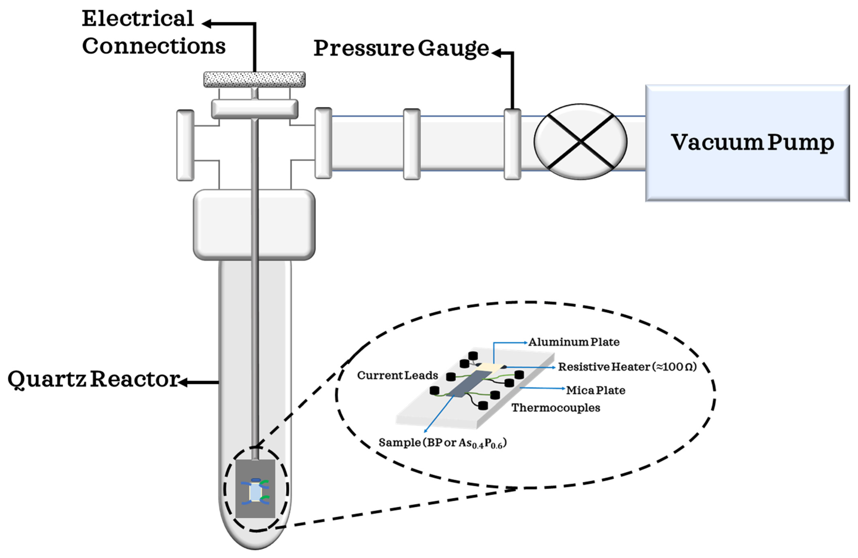
Abstract
:1. Introduction
2. Materials and Methods
2.1. Synthesis of Black Phosphorous and
2.2. Raman Spectroscopy
2.3. Electrical Transport Measurements
3. Results and Discussion
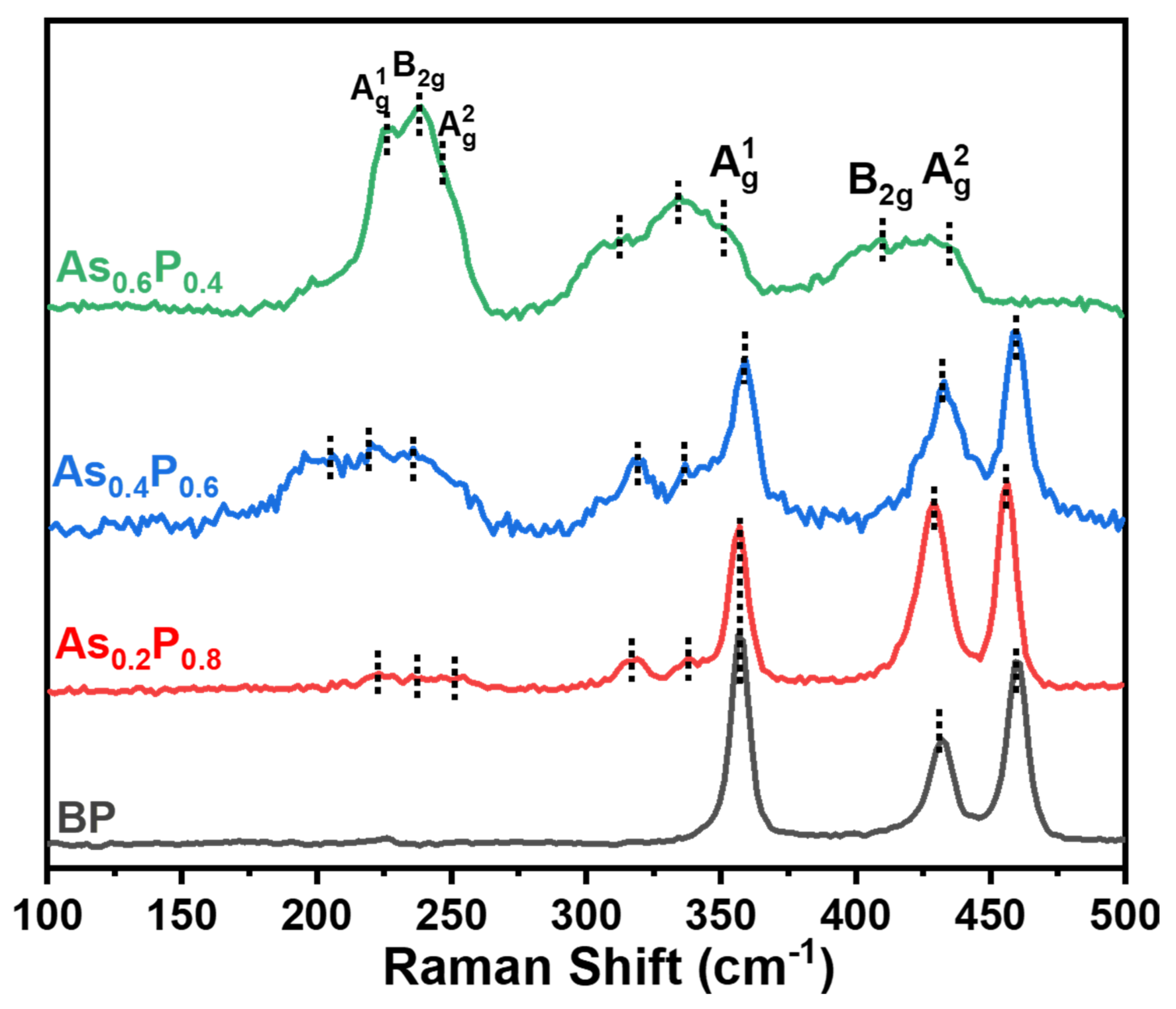
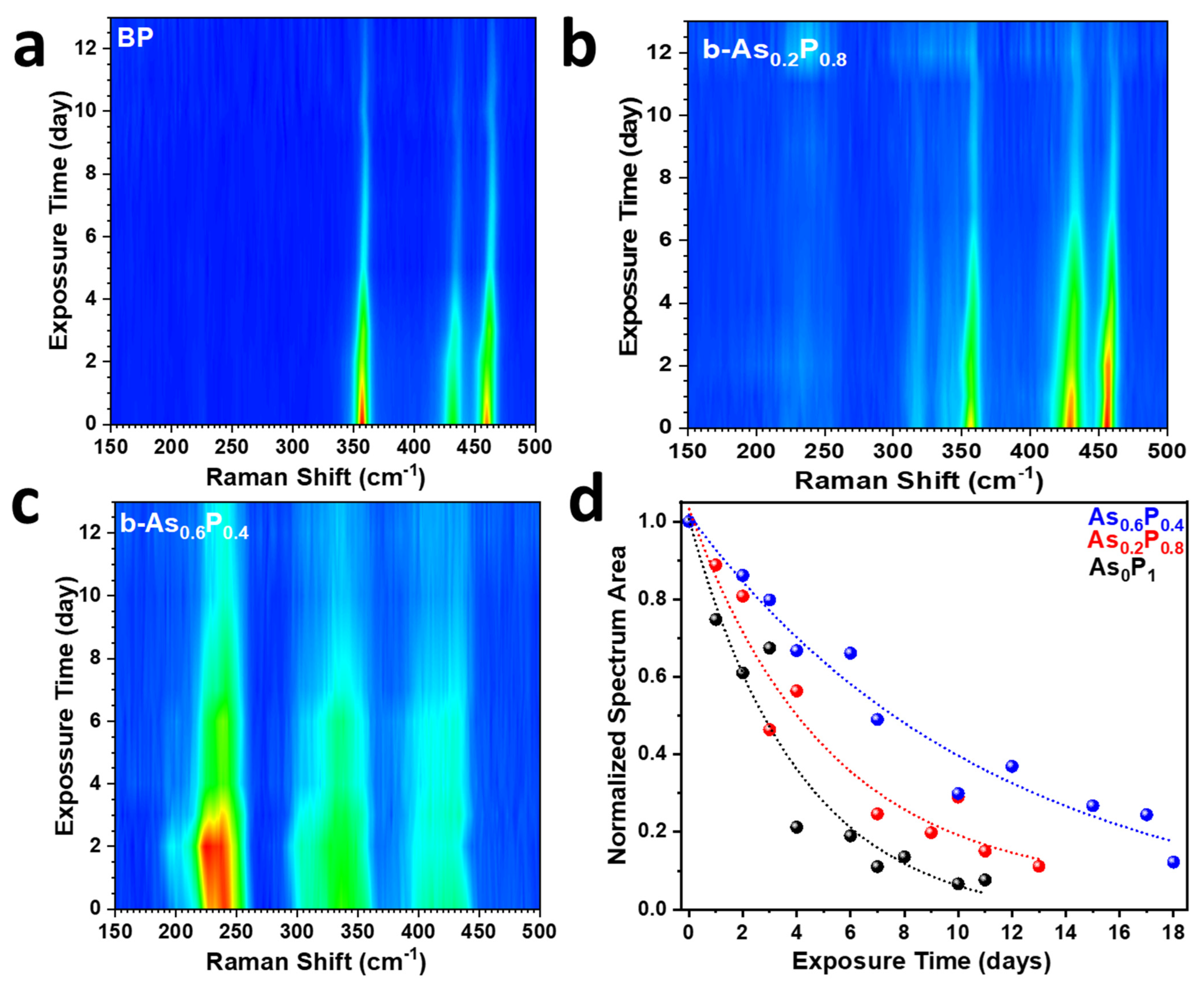
3.1. Raman Spectroscopy
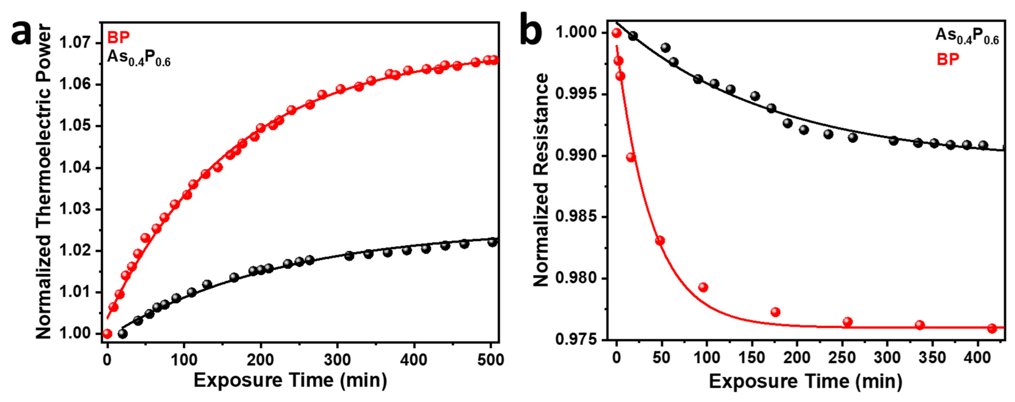
3.2. In situ Transport Property Measurements of BP and
4. Conclusions
Supplementary Materials
Author Contributions
Funding
Institutional Review Board Statement
Informed Consent Statement
Data Availability Statement
Conflicts of Interest
References
- Artel, V.; Guo, Q.; Cohen, H.; Gasper, R.; Ramasubramaniam, A.; Xia, F.; Naveh, D. Protective molecular passivation of black phosphorus. NPJ 2D Mater. Appl. 2017, 1, 6. [Google Scholar] [CrossRef]
- Yau, S.-L.; Moffat, T.P.; Bard, A.J.; Zhang, Z.; Lerner, M.M. STM of the (010) surface of orthorhombic phosphorus. Chem. Phys. Lett. 1992, 198, 383–388. [Google Scholar] [CrossRef]
- Castellanos-Gomez, A.; Vicarelli, L.; Prada, E.; Island, J.O.; Narasimha-Acharya, K.; Blanter, S.I.; Groenendijk, D.J.; Buscema, M.; Steele, G.A.; Alvarez, J. Isolation and characterization of few-layer black phosphorus. 2D Mater. 2014, 1, 025001. [Google Scholar] [CrossRef]
- Sang, D.K.; Wang, H.; Guo, Z.; Xie, N.; Zhang, H. Recent developments in stability and passivation techniques of phosphorene toward next-generation device applications. Adv. Funct. Mater. 2019, 29, 1903419. [Google Scholar] [CrossRef]
- Hyun, C.; Kim, J.H.; Lee, J.-Y.; Lee, G.-H.; Kim, K.S. Atomic scale study of black phosphorus degradation. RSC Adv. 2020, 10, 350–355. [Google Scholar] [CrossRef] [PubMed] [Green Version]
- Favron, A.; Gaufrès, E.; Fossard, F.; Phaneuf-L’Heureux, A.-L.; Tang, N.Y.W.; Lévesque, P.L.; Loiseau, A.; Leonelli, R.; Francoeur, S.; Martel, R. Photooxidation and quantum confinement effects in exfoliated black phosphorus. Nat. Mater. 2015, 14, 826–832. [Google Scholar] [CrossRef]
- Gamage, S.; Li, Z.; Yakovlev, V.S.; Lewis, C.; Wang, H.; Cronin, S.B.; Abate, Y. Nanoscopy of black phosphorus degradation. Adv. Mater. Interfaces 2016, 3, 1600121. [Google Scholar] [CrossRef]
- Li, Q.; Zhou, Q.; Shi, L.; Chen, Q.; Wang, J. Recent advances in oxidation and degradation mechanisms of ultrathin 2D materials under ambient conditions and their passivation strategies. J. Mater. Chem. A 2019, 7, 4291–4312. [Google Scholar] [CrossRef]
- Abate, Y.; Akinwande, D.; Gamage, S.; Wang, H.; Snure, M.; Poudel, N.; Cronin, S.B. Recent progress on stability and passivation of black phosphorus. Adv. Mater. 2018, 30, 1704749. [Google Scholar] [CrossRef]
- Wood, J.D.; Wells, S.A.; Jariwala, D.; Chen, K.-S.; Cho, E.; Sangwan, V.K.; Liu, X.; Lauhon, L.J.; Marks, T.J.; Hersam, M.C. Effective Passivation of Exfoliated Black Phosphorus Transistors against Ambient Degradation. Nano Lett. 2014, 14, 6964–6970. [Google Scholar] [CrossRef] [Green Version]
- Kim, J.-S.; Liu, Y.; Zhu, W.; Kim, S.; Wu, D.; Tao, L.; Dodabalapur, A.; Lai, K.; Akinwande, D. Toward air-stable multilayer phosphorene thin-films and transistors. Sci. Rep. 2015, 5, 8989. [Google Scholar] [CrossRef] [Green Version]
- Uk Lee, H.; Lee, S.C.; Won, J.; Son, B.-C.; Choi, S.; Kim, Y.; Park, S.Y.; Kim, H.-S.; Lee, Y.-C.; Lee, J. Stable semiconductor black phosphorus (BP)@ titanium dioxide (TiO2) hybrid photocatalysts. Sci. Rep. 2015, 5, srep08691. [Google Scholar] [CrossRef] [Green Version]
- Avsar, A.; Vera-Marun, I.J.; Tan, J.Y.; Watanabe, K.; Taniguchi, T.; Castro Neto, A.H.; Ozyilmaz, B. Air-stable transport in graphene-contacted, fully encapsulated ultrathin black phosphorus-based field-effect transistors. ACS Nano 2015, 9, 4138–4145. [Google Scholar] [CrossRef] [PubMed] [Green Version]
- Yang, B.; Wan, B.; Zhou, Q.; Wang, Y.; Hu, W.; Lv, W.; Chen, Q.; Zeng, Z.; Wen, F.; Xiang, J. Te-doped black phosphorus field-effect transistors. Adv. Mater. 2016, 28, 9408–9415. [Google Scholar] [CrossRef] [PubMed]
- Karki, B.; Rajapakse, M.; Sumanasekera, G.U.; Jasinski, J.B. Structural and Thermoelectric Properties of Black Arsenic–Phosphorus. ACS Appl. Energy Mater. 2020, 3, 8543–8551. [Google Scholar] [CrossRef]
- Han, R.; Feng, S.; Sun, D.-M.; Cheng, H.-M. Properties and photodetector applications of two-dimensional black arsenic phosphorus and black phosphorus. Sci. China Inf. Sci. 2021, 64, 140402. [Google Scholar] [CrossRef]
- Liang, J.; Hu, Y.; Zhang, K.; Wang, Y.; Song, X.; Tao, A.; Liu, Y.; Jin, Z. 2D layered black arsenic-phosphorus materials: Synthesis, properties, and device applications. Nano Res. 2021, 15, 3737–3752. [Google Scholar] [CrossRef]
- Tsai, Y.-C.; Bayram, C. Structural and electronic properties of hexagonal and cubic phase AlGaInN alloys investigated using first principles calculations. Sci. Rep. 2019, 9, 6583. [Google Scholar] [CrossRef] [Green Version]
- Xu, Y.; Shi, Z.; Shi, X.; Zhang, K.; Zhang, H. Recent progress in black phosphorus and black-phosphorus-analogue materials: Properties, synthesis and applications. Nanoscale 2019, 11, 14491–14527. [Google Scholar] [CrossRef]
- Chakrapani, V.; Angus, J.C.; Anderson, A.B.; Wolter, S.D.; Stoner, B.R.; Sumanasekera, G.U. Charge transfer equilibria between diamond and an aqueous oxygen electrochemical redox couple. Science 2007, 318, 1424–1430. [Google Scholar] [CrossRef] [Green Version]
- Desai, S.; Rivera, J.; Jalilian, R.; Hewaparakrama, K.; Sumanasekera, G. Studies of electronic distribution in potassium-doped mats of single-walled carbon nanotubes, double-walled carbon nanotubes, and peapods. J. Appl. Phys. 2008, 104, 013707. [Google Scholar] [CrossRef] [Green Version]
- Akhtar, M.; Zhang, C.; Rajapakse, M.; Musa, M.R.K.; Yu, M.; Sumanasekera, G.; Jasinski, J.B. Bilayer phosphorene under high pressure: In situ Raman spectroscopy. Phys. Chem. Chem. Phys. 2019, 21, 7298–7304. [Google Scholar] [CrossRef]
- Köpf, M.; Eckstein, N.; Pfister, D.; Grotz, C.; Krüger, I.; Greiwe, M.; Hansen, T.; Kohlmann, H.; Nilges, T. Access and in situ growth of phosphorene-precursor black phosphorus. J. Cryst. Growth 2014, 405, 6–10. [Google Scholar] [CrossRef] [Green Version]
- Rajapakse, M.; Musa, R.; Abu, U.O.; Karki, B.; Yu, M.; Sumanasekera, G.; Jasinski, J.B. Electrochemical Li intercalation in black phosphorus: In situ and ex situ studies. J. Phys. Chem. C 2020, 124, 10710–10718. [Google Scholar] [CrossRef]
- Abu, U.O.; Musa, M.R.K.; Rajapakse, M.; Karki, B.; Vithanage, D.; Yu, M.; Sumanasekera, G.; Jasinski, J.B. Vapor-Phase Intercalation of Cesium into Black Phosphorous. J. Phys. Chem. C 2021, 125, 27440–27448. [Google Scholar] [CrossRef]
- Abu, U.O.; Akter, S.; Nepal, B.; Pitton, K.A.; Guiton, B.S.; Strachan, D.R.; Sumanasekera, G.; Wang, H.; Jasinski, J.B. Ultra-Narrow Phosphorene Nanoribbons Produced by Facile Electrochemical Process. Adv. Sci. 2022, 9, 2203148. [Google Scholar] [CrossRef] [PubMed]
- Gómez-Pérez, J.; Barna, B.; Tóth, I.Y.; Kónya, Z.; Kukovecz, A.K. Quantitative tracking of the oxidation of black phosphorus in the few-layer regime. ACS Omega 2018, 3, 12482–12488. [Google Scholar] [CrossRef] [Green Version]
- Lide, D.R. CRC Handbook of Chemistry and Physics; CRC Press: Boca Raton, FL, USA, 2004; Volume 85. [Google Scholar]
- Qi, D.; Chen, W.; Gao, X.; Wang, L.; Chen, S.; Loh, K.P.; Wee, A.T. Surface transfer doping of diamond (100) by tetrafluoro-tetracyanoquinodimethane. J. Am. Chem. Soc. 2007, 129, 8084–8085. [Google Scholar] [CrossRef] [PubMed]
- Sque, S.J.; Jones, R.; Briddon, P.R. The transfer doping of graphite and graphene. Phys. Status Solidi 2007, 204, 3078–3084. [Google Scholar] [CrossRef]
- Suzuki, S.; Bower, C.; Watanabe, Y.; Zhou, O. Work functions and valence band states of pristine and Cs-intercalated single-walled carbon nanotube bundles. Appl. Phys. Lett. 2000, 76, 4007–4009. [Google Scholar] [CrossRef] [Green Version]
- Suzuki, S.; Watanabe, Y.; Homma, Y.; Fukuba, S.-Y.; Heun, S.; Locatelli, A. Work functions of individual single-walled carbon nanotubes. Appl. Phys. Lett. 2004, 85, 127–129. [Google Scholar] [CrossRef]
- Wang, Q.; Puntambekar, A.; Chakrapani, V. Co-adsorption of water and oxygen on GaN: Effects of charge transfer and formation of electron depletion layer. J. Chem. Phys. 2017, 147, 104703. [Google Scholar] [CrossRef] [PubMed]
- Chakrapani, V.; Pendyala, C.; Kash, K.; Anderson, A.B.; Sunkara, M.K.; Angus, J.C. Electrochemical pinning of the Fermi level: Mediation of photoluminescence from gallium nitride and zinc oxide. J. Am. Chem. Soc. 2008, 130, 12944–12952. [Google Scholar] [CrossRef]
- Chandel, M.; Thakur, M.; Sharma, A.; Pathania, D.; Kumar, A.; Singh, L. Chlorophyll sensitized (BiO)2CO3/CdWO4/rGO nano-hybrid assembly for solar assisted photo-degradation of chlorzoxazone. Chemosphere 2022, 305, 135472. [Google Scholar] [CrossRef] [PubMed]
- Cai, Y.; Zhang, G.; Zhang, Y.-W. Layer-dependent band alignment and work function of few-layer phosphorene. Sci. Rep. 2014, 4, 6677. [Google Scholar] [CrossRef] [Green Version]


Disclaimer/Publisher’s Note: The statements, opinions and data contained in all publications are solely those of the individual author(s) and contributor(s) and not of MDPI and/or the editor(s). MDPI and/or the editor(s) disclaim responsibility for any injury to people or property resulting from any ideas, methods, instructions or products referred to in the content. |
© 2023 by the authors. Licensee MDPI, Basel, Switzerland. This article is an open access article distributed under the terms and conditions of the Creative Commons Attribution (CC BY) license (https://creativecommons.org/licenses/by/4.0/).
Share and Cite
Abu, U.O.; Vithanage, D.; Vitharana, A.; Jasinski, J.B.; Sumanasekera, G. Degradation Studies of Air-Exposed Black Phosphorous and Black Arsenic Phosphorous. ChemEngineering 2023, 7, 18. https://doi.org/10.3390/chemengineering7020018
Abu UO, Vithanage D, Vitharana A, Jasinski JB, Sumanasekera G. Degradation Studies of Air-Exposed Black Phosphorous and Black Arsenic Phosphorous. ChemEngineering. 2023; 7(2):18. https://doi.org/10.3390/chemengineering7020018
Chicago/Turabian StyleAbu, Usman O., Dinushika Vithanage, Ashan Vitharana, Jacek B. Jasinski, and Gamini Sumanasekera. 2023. "Degradation Studies of Air-Exposed Black Phosphorous and Black Arsenic Phosphorous" ChemEngineering 7, no. 2: 18. https://doi.org/10.3390/chemengineering7020018