Article

The Influence of Different Recombination Pathways on Hysteresis in Perovskite Solar Cells with Ion Migration

1
State Key Laboratory of Silicon Materials and School of Materials Science and Engineering, Zhejiang University, Hangzhou 310027, China
2
Sichuan Research Center of New Materials, Institute of Chemical Materials, China Academy of Engineering Physics, 596 Yinhe Road, Chengdu 610200, China
3
Zhejiang Aiko Solar Energy Technology Co., Ltd., 699 Haopai Road, Yiwu 322000, China
4
School of Materials Science and Engineering, Zhengzhou University, Zhengzhou 450001, China
*
Authors to whom correspondence should be addressed.
These authors contributed equally to this work.
Inorganics 2023, 11(2), 52; https://doi.org/10.3390/inorganics11020052
Submission received: 12 December 2022 / Revised: 13 January 2023 / Accepted: 17 January 2023 / Published: 19 January 2023
(This article belongs to the Special Issue Inorganics: 10th Anniversary)

Abstract

:
The impact of hysteresis on the power conversion efficiency (PCE) of perovskite solar cells (PSCs) still faces uncertainties despite the rapid development of perovskite photovoltaics. Although ion migration in perovskites is regarded as the chief culprit for hysteresis, charge carrier recombination pathways in PSCs are proposed to be necessary for the occurrence of hysteresis. Here, the impact of both bulk recombination and interface recombination on hysteresis in PSCs is investigated via drift–diffusion modeling. The simulation results demonstrate a direct correlation between recombination pathways and hysteresis in PSCs with ion migration. The simulation reveals that recombination pathways in PSCs will react to the variation in charge carrier distribution under different voltage scanning directions induced by ion migration in absorber layers, which leads to hysteresis in PSCs. Moreover, the hysteresis in normal (N-I-P) PSCs with different electron transport layers (ETLs) including sintered SnO2, SnO2 nano crystals and TiO2 is experimentally explored. The results demonstrate that multiple recombination pathways coupled with ion migration can lead to obvious hysteresis in fabricated PSCs which is consistent with simulation results. This work provides great insight into hysteresis management upon composition, additive and interface engineering in PSCs.

Graphical Abstract

1. Introduction

PSCs have rapidly progressed in the last ten years, with the record power conversion efficiency (PCE) of up to 25.7% to date [1]. Due to their advantages, i.e., low-cost processing, abundant raw materials and high absorption coefficients, PSCs have risen to be the photovoltaic technique with the most potential for next-generation solar cells [2,3,4,5,6]. However, anomalous hysteresis in PSCs adds uncertainties to the steady-state output efficiency and operational stabilities of PSCs, thus limiting the commercialization for PSCs [7,8,9,10]. Interface states, ferroelectric properties and ion migration were first proposed to be the underlying process for hysteresis [7,11]. Since then, enormous work efforts have been paid to understanding and suppressing hysteresis [12]. Targeting the hysteresis in PSCs [9,13,14,15,16], composition engineering [17,18,19], interface engineering [11,20,21] and additive engineering [22,23,24] were proved to be effective in mitigating hysteresis in PCSs, yet it remains hard to completely eliminate it, which calls for deeper understanding of the physics behind hysteresis in PSCs.
Mobile ions in perovskite films can migrate under built-in electric fields or bias voltages which redistribute the electric field across absorber layers [13,14,25,26,27]. Once a voltage scan begins, mobile ions in absorber layers will react to the external voltage, which changes the electric potential distribution in PSCs, resulting in a disparity in the efficiency of PSCs when the voltage scanning direction varies [28,29]. Therefore, mobile ions are believed to be responsible for hysteresis in PSCs. In addition, the current transient in PSCs indicates that multiple processes are responsible for hysteresis, including mobile ions [30]. Moreover, interface passivation with PCBM or by forming a 2D perovskite layer leads to significantly suppressed hysteresis, suggesting that interface recombination is related to hysteresis problems [11,20]. Furthermore, transient measurements and simulations based on the diffusion–drift model suggest that mobile ions and recombination near the perovskite–contact interfaces are necessary for hysteresis in PSCs [31]. In addition, the fact that a modulation of charge carrier lifetime by composition engineering leads to suppressed hysteresis implies that there might be a correlation between bulk recombination and hysteresis in PSCs [19,24]. Based on drift–diffusion modeling, it is presented that charge carrier diffusion length (L) is related to the extent of hysteresis in PSCs, which also hints at the connection between recombination pathways and hysteresis [32]. These results suggest an underlying correlation between recombination pathways and hysteresis in PSCs. To the best of our knowledge, the systematic study of the influences of different recombination pathways on hysteresis in PSCs with ion migration is not well investigated.
Here, the influences of different recombination pathways (bulk recombination and interface recombination) on hysteresis in PSCs are investigated via drift–diffusion modeling [33]. The simulation results suggest that only the coexistence of severe recombination pathways and ion migration can lead to severe hysteresis in PSCs. The underlying mechanism is that the recombination pathways in PSCs will react to the variation in charge carrier distribution under different voltage scanning directions induced by ion migration in absorber layers, which generates hysteresis in PSCs. Moreover, the simulations demonstrate that bulk recombination tends to lead to obvious hysteresis in PSCs when L is smaller than the thickness of the absorber layer. Moreover, the recombination at both ETL/perovskite and hole-transporting layer (HTL)/ perovskite interfaces can worsen the hysteresis in PSCs with ion migration. Temperature-dependent hysteresis results based on different ETLs (sintered SnO2, SnO2 nanocrystals and TiO2) imply the observed hysteresis is associated with ion migration in perovskite layers. The results related to charge carrier lifetime and temperature-dependent open-circuit voltage suggest both bulk recombination and interface recombination are responsible for hysteresis in the fabricated PSCs, which is consistent with the simulation results. This work provides great insight into hysteresis problems in PSCs.

2. Results and Discussion
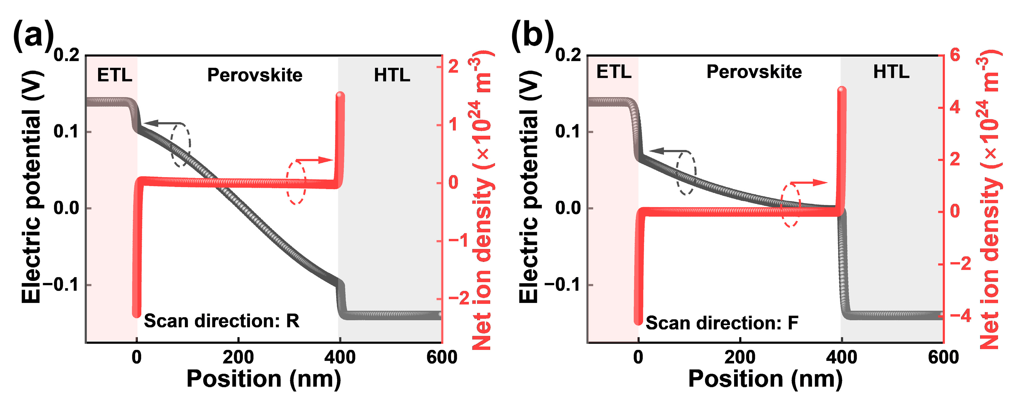
2.1. Ion Migration

First, the role of ion migration played in hysteresis in PSCs was explored via diffusion–drift modeling. Since hysteresis was now obvious in PSCs with N-I-P configuration, the simulation was performed in PSCs with the configuration of SnO2/MAPbI3 (Methylammonium lead iodide)/Spiro-OMeTAD. Here, we assumed negligible bulk recombination and interface recombination in PSCs to solely investigate the influence of ion migration on the performance of PSCs. The simulation parameters are detailed in the supporting information and Table S1. Note that the absorber layer in the drift–diffusion modeling was of 400 nm. Here, the appropriate density of iodine vacancies was assumed in the simulation with a presumed diffusion coefficient [13,15,16,34]. The electric potential and net ion density distribution were simulated as shown in Figure 1, which shows that electric potential and net ion density distribution differed under different voltage scanning directions. The changes in the electric potential across PSCs were the direct results induced by ion migration. Moreover, the change in electric potential would affect the distribution of charge carriers in absorber layers since the quasi-Fermi level at a specific position in absorber layers was determined by the electric potential across PSCs. Indeed, Figure S1 shows both electron and hole density change when the voltage scanning direction changes, which demonstrates the influence of ion migration on the charge carrier distribution in PSCs. The recombination pathways in PSCs, if any, will react to a change in the distribution of charge carriers and to a variation in recombination loss in PSCs, which might lead to a disparity in the J-V curves between different voltage scanning directions, namely hysteresis in PSCs. Note that the ion migration may not induce hysteresis in PSCs when there is negligible recombination in PSCs. The influence of mobile ions alone on hysteresis in PSCs was simulated with negligible recombination in PSCs. Figure S2 shows that there was no apparent hysteresis with a wide range of density of mobiles in the absorber layers under the work condition voltage scanning rate. Moreover, the distribution of mobile ions at different voltages near the interface between charge-transporting layers and perovskite films was simulated as shown in Figure S3. It is shown that the mobile ions migrated during the voltage scan. However, the ion migration led to no hysteresis in the J-V curves, as shown in Figure S2. These results suggest that recombination pathways might be necessary for apparent hysteresis in PSCs with ion migration. In the following section, the influence of a specific recombination pathway on hysteresis in PSCs with ion migration is explored.

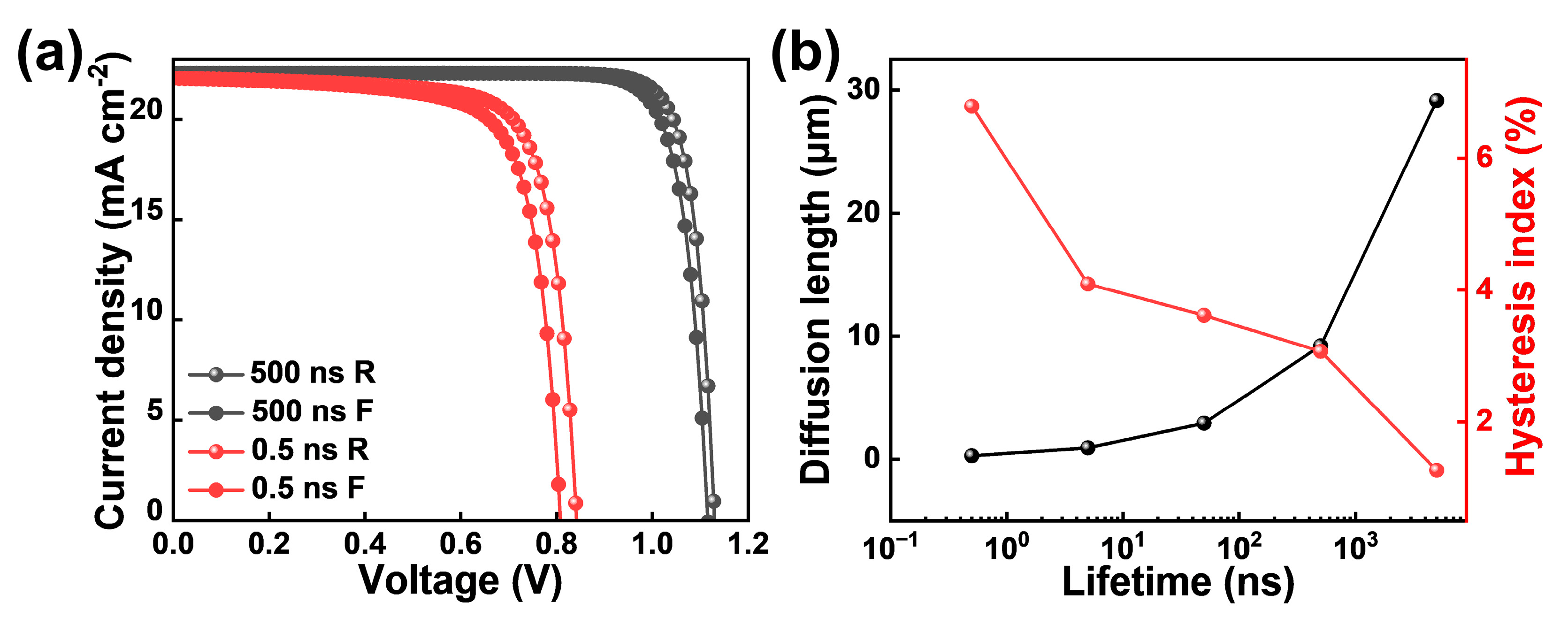
2.2. Bulk Recombination

Here, the influence of bulk recombination on hysteresis in PSCs with ion migration is explored. For perovskite absorber layers, bulk recombination takes the form of Shockley–Read–Hall (SRH), radiative and Auger recombination [35]. However, for a PSC operating under 1 Sun (AM 1.5, 100 mW cm−2) illumination, SRH recombination is the dominant bulk recombination pathway, which limits the efficiency of a solar cell below its radiative limit [36]. Therefore, SRH recombination is assumed as the only recombination pathway for bulk recombination in drift–diffusion modeling to simplify the simulation while retaining the physical essence. Here, charge carrier lifetime was chosen as the parameter to reflect the extent of SRH recombination in PSCs, and the hole lifetime was set to be equal with the electron lifetime in the simulation. Note that the specific details of defects which induce SRH recombination such as the energy level and the capture cross-section were not considered in the simulation. Moreover, interface recombination was omitted in the simulation by setting a negligible recombination velocity (1 × 10⁻³ cm s−1) at both the charge-transporting layer/absorber layer interfaces.
The effects of ion migration and bulk recombination on hysteresis are demonstrated in Figure S4. Figure S4a,b show that mobile ions alone cannot result in hysteresis for a PSC. Figure S4a,c show that bulk recombination alone cannot lead to hysteresis in PSCs. Furthermore, the combination of bulk recombination and ion migration can lead to obvious hysteresis in PSCs, as shown in Figure S4d. Moreover, as bulk recombination in PSCs gets worse, as shown in Figure 2, PSCs experience severer hysteresis, which indicates a direct correlation between bulk recombination and hysteresis problems. In addition, the hysteresis index (HI) was utilized to quantify the extent of hysteresis in PSCs, described as follows:
HI = P C E R P C E F P C E R
where PCER is the PCE in the reverse scanning direction (from high voltage to low voltage). PCEF is the PCE in the forward scanning direction (from low voltage to high voltage). Carrier lifetime versus HI curves are plotted in Figure 2b. Figure 2b shows that HI experiences a rapid increase when the carrier lifetime decreases from 5 ns to 0.5 ns. It is well-known that carrier lifetime is related to carrier diffusion length (L) through
L = D τ
where D is the diffusion coefficient of a charge carrier. When perovskite films have a charge carrier lifetime of 0.5 ns, the L is ~290 nm based on the assumed D, which is smaller than the thickness of the absorber layer. This result indicates that the bulk recombination tends to significantly influence hysteresis in PSCs when the L is smaller than the thickness of the perovskite layer. Moreover, these results suggest that the small amount of hysteresis in the state-of-the-art normal PSCs may be attributed to the greatly mitigated bulk recombination in these devices.

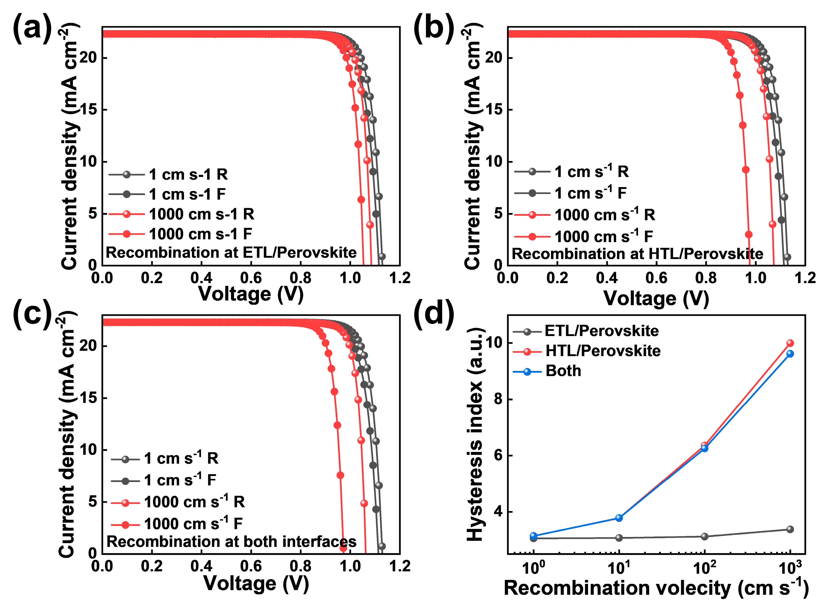
2.3. Interface Recombination

The protocol for the simulation described in this section involves the influence of interface recombination on hysteresis. Interface recombination has different forms, as depicted by Krückemeier et.al [37]. Here, in the simulation, the interface recombination was mainly in the form of interface-defect-related interface recombination, which is consistent with previous works [29,32]. The extent of interface recombination is modulated by changes in the interface recombination velocity. Note that the details of interface defects such as the energy level and the capture cross-section are not considered in the simulation. The bulk recombination was set for 500 ns, which showed minor influence on hysteresis, as shown in Figure 2. Note that for each interface, the electron recombination velocity was set to be equal to the hole recombination velocity. First, we focused on the interface recombination at the interface between ETL and absorber layers, while the interface recombination at the interface between HTL and absorber layers was omitted by setting a negligible interface recombination velocity of 1 × 10⁻³ cm s−1. The simulation results in Figure 3a show that the increase in interface recombination at the ETL/perovskite interface could lead to worse hysteresis in PSCs. Note that Figure S5b shows interface recombination at the ETL/perovskite interface, and bulk recombination will not lead to hysteresis with negligible ion migration.
Subsequently, the influence of interface recombination in the HTL/perovskite layer on hysteresis was investigated. Here, the interface recombination velocity at the HTL/perovskite interface was modulated, while the interface recombination velocity at the ETL/Perovskite layer was set to a negligible value of 1 × 10⁻³ cm s−1. Figure 3b shows the simulation results, which demonstrate worse hysteresis at a bigger interface recombination velocity. Figure 3c shows the simulation results of the same interface recombination velocity at both the ETL/perovskite and HTL/perovskite interfaces. The summarized hysteresis index versus interface recombination velocity plot is shown in Figure 3d. The simulation results demonstrate that there is a direct connection between the extent of interface recombination and hysteresis in PSCs with ion migration. Note that the mobile ion is a necessary factor for hysteresis when severe interface recombination exists in PSCs, as shown in Figure S5c. Interestingly, Figure 3b,d show that the interface recombination at the HTL/perovskite interface may have a stronger impact on hysteresis than that of the ETL/perovskite interface. Further simulation showed that a stronger influence of the HTL/perovskite interface on hysteresis in the simulation was related to the difference in permittivity between transporting layers, as shown in Figure S6. Note that the permittivity adopted for ETL and HTL layers in the simulation in Figure 3 was similar to the real condition for N-I-P PSCs. Future works might be dedicated to the systematic investigation of the influence of the difference in permittivity between charge-transporting layers on hysteresis in PSCs.

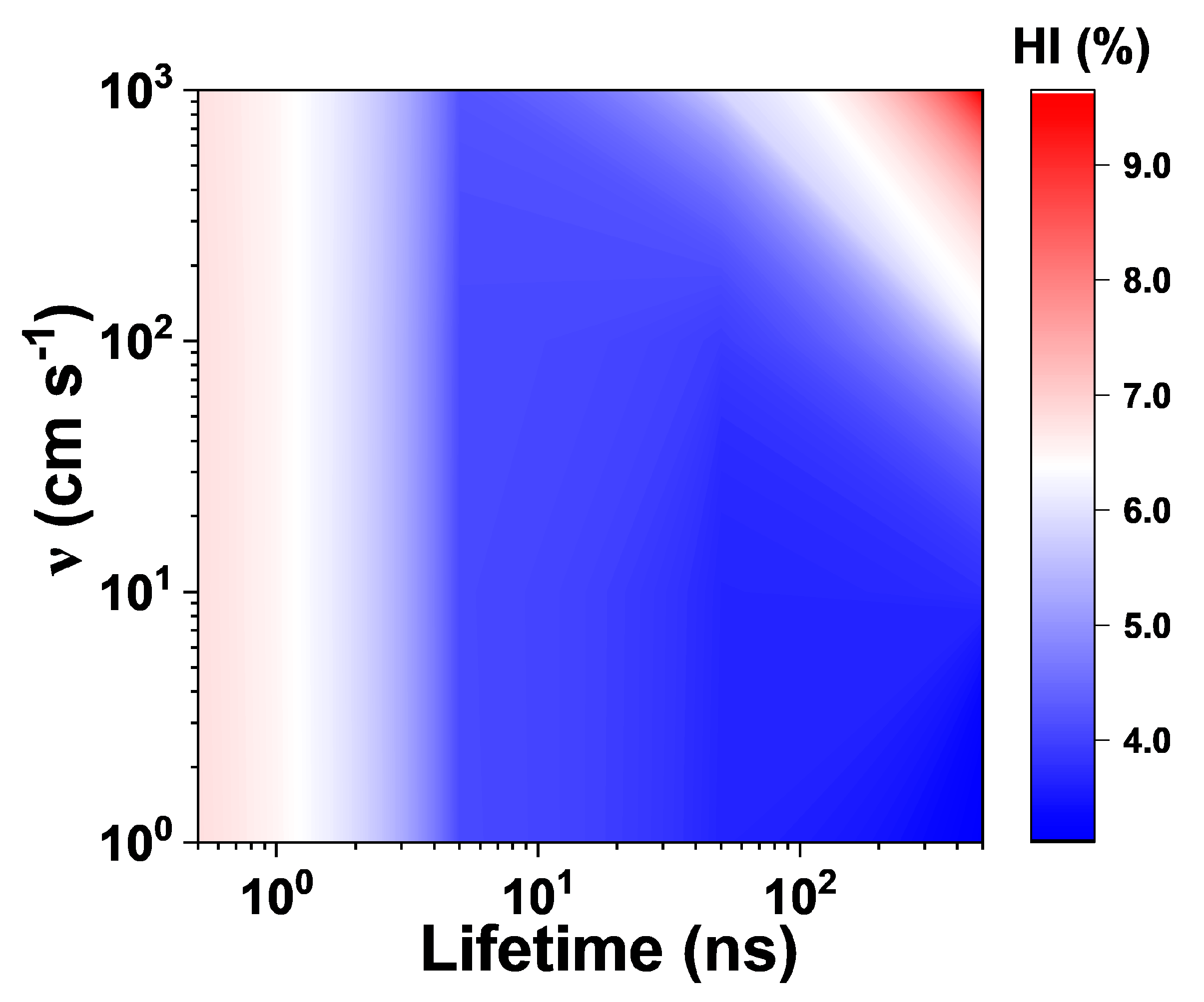
2.4. Bulk Recombination and Interface Recombination

Finally, the J-V curves of the device with both interface recombination and bulk recombination coupled with ion migration were simulated. Here, both interface recombination at the ETL/perovskite and HTL/perovskite interfaces were considered with the same interface recombination velocity (v). Bulk recombination was considered in the same way as in the bulk recombination part above. The simulation results are presented in Figure 4 as a pseudo color map. Surprisingly, severe bulk recombination coupling with severe interface recombination does not lead to much worse hysteresis in PSCs. Instead, as shown in Figure 4, when there is severe bulk recombination (L < d) in an absorber layer, interface recombination will have a minor influence on hysteresis in PSCs. Moreover, when mild bulk recombination exists in an absorber layer, severe interface recombination can lead to a severe hysteresis problem. Note that the mobile ion is a necessary factor for hysteresis when both severe bulk recombination and severe interface recombination exists in PSCs, as shown in Figure S5d. Moreover, even though simulations were performed on PSCs with N-I-P configurations, the results may provide some guidance on hysteresis in inverted (P-I-N) PSCs if the properties of their charge-transporting layers are similar to each other. Figure S7 demonstrates simulations of J-V curves of both N-I-P and P-I-N PSCs with the same condition (mobile ions, recombination pathways and properties of charge-transporting layers). It shows that the hysteresis in both PSCs is rather similar. Overall, the simulation results reveal the influences of recombination pathways on hysteresis in perovskite solar cells with ion migration.

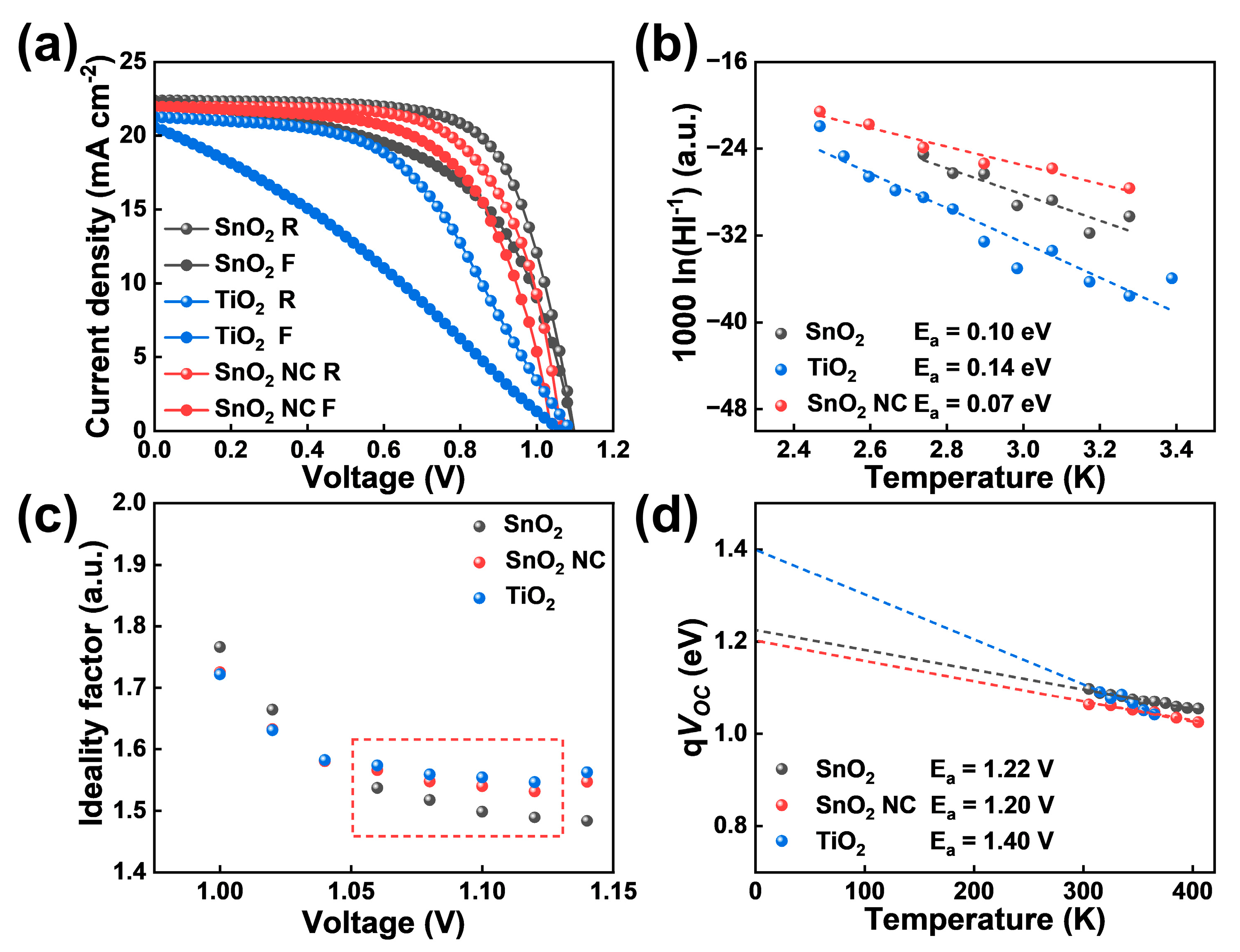
2.5. Hysteresis in Fabricated Devices

Here, PSCs with normal structures of ITO/ETL/MAPbI3/Spiro-OMeTAD/Au with different ETLs were fabricated. Sintered SnO2, SnO2 nanocrystals (NCs) and TiO2 ETL materials were chosen for they are widely used in highly efficient PSCs. The fabrication details are presented in the supporting information. The scanning electron microscope (SEM) images of perovskite films grown on different substrates are displayed in Figure S8. The SEM images show that there was a small difference in the average grain size of the resultant perovskite films, which indicates that the crystal growth dynamics of perovskites may be influenced by these ETLs. J-V curves of these PSCs at room temperature are displayed in Figure 5a. The parameters, such as open-circuit voltage (VOC), current density (JSC) and fill factor (FF) are presented in Table 1. As shown in Table 1, TiO2 devices demonstrate the largest HI of 42.78%, while SnO2 NC devices demonstrate the smallest HI of 15.86%. Moreover, hysteresis in these devices at different temperatures was measured. The results show that HI in PSCs decreases with temperature, implying that ion migration is the underlying process, since the diffusion coefficient increases with temperature, which makes ion migration follow the voltage scanning speed, resulting in a decrease in hysteresis [38]. In addition, the HI (ln(HI−1)) versus temperature (K−1) curve could be well fitted using the Arrhenius equation, which generates activation energy (Ea), as shown in Figure 5b. The extracted Ea was in the range of 0.07–0.14 eV, which is consistent with the reported activation energy of ion migration in the literature [13,14,15,16]. The slightly different Ea in the devices with different ETLs may be attributed to the different crystal growth dynamics of perovskite films on different ETLs, as suggested by the SEM images.
The recombination mechanism in PSCs was first investigated using ideality factors (n) extracted from dark J-V curves from PSCs, as described in the following equation [39]:
J = J 0 exp q V n k T 1
where J0 is an exponential pre-factor; k is the Boltzmann constant; T is temperature in the unit of K. Since the ideality factors are not constant in dark J-V curves, differential ideality factors were extracted to study the recombination mechanisms in PSCs [39]. Figure 5c shows the differential ideality factors around the exponential region of the dark J-V curves. The differential ideality factors stabilized at 1.05 V and then tended to increase mainly due to the parasitic resistance. The stabilized differential ideality factors at 1.05 V are seen as the ideality factors for the PSCs. Therefore, the fabricated PSCs have n between 1.5 and 1.6. Moreover, the differences in n between these PSCs are small, which suggests a similar extent of overall nonradiative recombination in these PSCs. An n between 1 and 2 along with a VOC of ~1.10 V can indicate that the resultant PSCs suffer from SRH recombination in the bulk of perovskite films [39,40]. The extent of interface recombination in the fabricated PSCs is discussed below. Moreover, bulk recombination in perovskite layers was investigated via TRPL, as shown in Figure S9a. Exponential fitting was performed on the TRPL data, which showed a charge carrier lifetime of 56.84 ns. The details of the simulation results are presented in the supporting information in Table S2. Note that a charge carrier lifetime of 56.84 ns coupled with ion migration would lead to hysteresis in the fabricated PSCs, as shown in Figure 2b. In addition, to further investigate the recombination pathway in the fabricated PSCs, temperature-dependent VOC tests were performed, as shown in Figure 5d. A temperature-dependent VOC can be described through [39]
q V O C = E a A k T
where q is elemental charge; Ea is activation energy. For a device dominated by bulk recombination, the Ea extracted from temperature dependence will be close to the bandgap (Eg) of the absorber layer. Note that the Eg of MAPbI3 was ~1.6 eV. A small Ea compared to Eg may have been caused by non-selective contacts, tail states or interface recombination in PSCs [39]. First, it is not the case that it was caused by non-selective contact since the fabricated devices had both charge-transporting layers. Moreover, Urbach energy (EU)—the characteristic energy of tail states—was extracted from the UV-vis data, which was 45 meV, as shown in Figure S9b [41]. The small EU of the tail states was not consistent with the energy difference between Ea and Eg shown in Figure 5d. Therefore, the small activation energy in Figure 5d suggests that there may have been severe interface recombination in the fabricated PSCs. Figure 5d demonstrates that the Ea between SnO2 and SnO2 NC were close, which were ~1.2 eV smaller than the Eg of MAPbI3. The similar Ea for SnO2 and SnO2 NC devices is reasonable, since they are of the same species of materials. The TiO2 device demonstrated an Ea of 1.4 eV. In addition, the bigger Ea in the TiO2 device compared to that in the SnO2 and SnO2 NC devices suggests that there is less interface recombination in TiO2 devices. However, the similar ideality factor in these PSCs indicate a similar overall nonradiative recombination loss in these PSCs. Combining the results in Figure 5c,d, it can be inferred that the defect distributions are slightly different between these PSCs. The bulk recombination may have been more severe in the TiO2 device. Overall, Figure 5b–d demonstrates that both bulk recombination and interface recombination in PSCs coupled with ion migration cause the observed hysteresis in PSCs, which is consistent with the results in drift–diffusion modeling.

3. Experimental Section

3.1. Materials

MAI, PbI2, SnCl2·2H2O, Ti(iv) bis(ethylacetoacetal)-diisopropoxide and Spiro-OMeTAD were purchased from Xi’an Polymer Light Technology Corp, Xi’an, China. SnO2 H2O colloidal dispersion liquid was purchased from Alfa Aesar, Ward Hill, MA, USA. Dimethyl formamide (DMF), dimethyl sulfoxide (DMSO), chlorobenzene and ethyl acetate were purchased from Sigma-Aldrich, St. Louis, MI, USA. Ethyl alcohol was purchased from Aladdin Industrial Corp, Shanghai, China. Diethyl ether was purchased from Sinopharm Chemical Reagent Co., Ltd., Shanghai, China ITO substrates were purchased from Hangzhou Hong Shi Technology Corp, Hangzhou, China.

3.2. Fabrication of Perovskite Solar Cells

The ITO and FTO glasses were sequentially cleaned in deionized water, ethyl alcohol, acetone and isopropanol via sonication for 5 min. SnO2 were prepared by spin-coating precursor solutions of SnCl2·2H2O in ethanol with 23 mg/mL of the clean ITO substrates at 3000 rpm for 30 s and annealing them in air at 180 °C. For SnO2 NC, a SnO2 precursor solution was obtained by mixing 15% SnO2 water colloidal dispersion liquid with deionized water with a volume ratio of 1:5. The precursor solution was spin-coated onto ITO glasses at 3000 rpm for 30 s. A SnO2 layer was annealed under ambient air at 150 °C for 1 h. For the compact TiO2 layer, TiO2 was deposited on the clean FTO glass via spray pyrolysis with 0.4 M Ti (iv) bis(ethylacetoacetal)-diisopropoxide in ethanol solution, which was then annealed in air at 550 °C for 60 min and kept at 150 °C before use. MAPbI3 perovskite precursor solution was prepared by mixing PbI2 (461 mg), MAI (159 mg) and DMSO (78 μL) in DMF (630 μL) solvent and then spin-coating it onto ETLs using a process of 1000 rpm for 10 s and 5000 rpm for another 20 s. Diethyl ether (500 μL) was dropped onto substrate about 15 s after the spin-coating procedure began. Then, the substrates were annealed at 75 °C for 1 min and 105 °C for 10 min to crystallize the perovskite films. For Spiro-OMeTAD solution, 17.5 μL of Li-TFSI acetonitrile solution (520 mg mL−1) and 28.75 μL of TBP were added into a 72.25 mg mL−1 Spiro-OMeTAD Chlorobenzene solution. Spiro-OMeTAD layers were spin-coated onto perovskite films at 3000 rpm for 30 s. Finally, 100 nm of Au was deposited on the top of the Spiro-OMeTAD hole-transporting layers (HTLs) under a vacuum of less than 1 × 10⁻³ Pa via a thermal evaporation system.

3.3. Device and Material Characterization

For all devices, the photovoltaic performance was measured by masking on the active area with a metal mask (certified area was 0.08567 cm2). The current density–voltage (J−V) curves of solar cells were measured using a Keithley 2400 source meter with a solar simulator (94022A, Newport Corp, Irvine, United States) with a KG5 filter. The J−V measurements were carried out in ambient air. The sweeping conditions were: forward to reverse scan (R: 1.2 V to −0.2 V, delay time 200 ms) and reverse to forward scan (F: −0.2 V to 1.2 V, delay time 200 ms). The temperature-dependent measurement was performed on a customized temperature stage. The time-resolved photoluminescence (TRPL) spectroscopy was measured with a PL spectrometer (FLS 920, Edinburgh Instruments, Livingston, United Kingdom). The samples were excited by a pulsed laser, with a wavelength and frequency of 405 nm and 1 MHz.

3.4. Diffusion–Drift Modeling

We used the drift diffusion simulator, IonMonger [33], which incorporates mobile ions into the model, to explore hysteresis in PSCs with ion migration. The device parameters are listed in Table S1, most of which are set close to the real device parameters based on the literature. Time-varying voltage/illumination protocols are specified as follows: The device was firstly kept in the dark for 5 s to examine whether a steady state was reached, followed by a reverse scan from 1.2 V to 0 V at a scan rate of 1.2 V s−1 under illumination, followed by a scan from 0 V to 1.2 V at the same scan rate. Note that the scan rate was close to the real scanning condition of solar cells. The effect of scan rates on hysteresis is demonstrated in Figure S10. From the simulation results, we note that that only the condition of recombination coupling with ion migration leads to the hysteresis problem in PSCs. Severe recombination with negligible ion migration in perovskite films does not result in hysteresis in PSCs, as shown in Figure S5.

4. Conclusions

Here, the influence of different recombination pathways on hysteresis in PSCs coupled with ion migration was investigated via drift–diffusion modeling. The simulation demonstrated that a single recombination pathway, either bulk recombination or interface recombination coupled with ion migration, can lead to hysteresis in PSCs. Bulk recombination in combination with interface recombination coupled with ion migration can lead to worse hysteresis problems in PSCs. The mechanism is that recombination pathways in PSCs will react to the variation in charge carrier distribution under different voltage scanning directions induced by ion migration in absorber layers, which results in hysteresis in PSCs. In addition, the investigation of the hysteresis in fabricated PSCs of normal configurations with different ETLs (sintered SnO2, SnO2 NCs and TiO2) suggests both bulk recombination and interface recombination were responsible for the hysteresis in the fabricated PSCs, which is consistent with the simulation results. Further work should focus on the influence of the details of recombination pathways, such as the distribution of defects in absorber layers, the energy level of the defect and the capture cross-section of the defect, on hysteresis in PSCs. This work provides a deeper understanding of hysteresis associated with detrimental recombination in PSCs.

Supplementary Materials

The following supporting information can be downloaded at: https://www.mdpi.com/article/10.3390/inorganics11020052/s1, Figure S1: Charge carrier distribution in perovskite layers in different voltage scanning directions: (a) electrons; (b) holes. Figure S2: The simulation of J-V curves for PSCs with same negligible recombination and with different density of mobile ions: (a) 1.6 × 1024 m−3; (b) 1.6 × 1025 m−3; (c) 1.6 × 1026 m−3; (d) 1.6 × 1027 m−3. Figure S3: The distribution of mobile ions at different voltages near the interface between charge-transporting layers and perovskite films. The density of mobile ions for the simulation is 1.6 × 1025 m−3. (a) ETL/perovskite interface; (b) HTL/perovskite interface. Figure S4: (a) J-V curves for a PSC with negligible bulk recombination and negligible density of mobile ions; (b) J-V curves for a PSC with negligible bulk recombination and high density of mobile ions; (c) J-V curves for a PSC with severe bulk recombination and negligible density of mobile ions; (d) J-V curves for a PSC with severe bulk recombination and high density of mobile ions. Figure S5: (a) Only severe bulk recombination coupled with negligible ion migration; (b) only severe interface recombination at ETL/perovskite interface coupled with negligible ion migration; (c) only severe interface recombination at HTL/perovskite interface coupled with negligible ion migration; (d) severe bulk recombination with severe interface recombination at both interfaces coupled with negligible ion migration. Figure S6: J-V curves for interface recombination at ETL/perovskite and HTL/perovskite interface: (a) same thickness, same relative permittivity and same diffusion coefficient for transporting layers; (b) different thickness, same relative permittivity and same diffusion coefficient for transporting layers; (c) different thickness, same relative permittivity and same diffusion coefficient for transporting layers; (d) different thickness, same relative permittivity and same diffusion coefficient for transporting layers; Figure S7: J-V curves for both N-I-P and P-I-N PSCs under same condition: (a) N-I-P; (b) P-I-N. Figure S8: SEM images for the perovskite films on different substrates. (a) SnO2; (b) SnO2 NC; (c) TiO2. The scale bar is 1 μm. Figure S9: (a) TRPL data for perovskite films with the structure of glass/MAPbI3. (b) Urbach energy for perovskite films with the structure of glass/MAPbI3. Figure S10: The effect of scan rates on hysteresis in PSCs. The carrier lifetime is 500 ns. The interface recombination velocity is 100 cm/s for both holes and electrons at both ETL/perovskite and HTL/perovskite interface. (a) 0.1 V/s; (b) 0.6 V/s; (c) 1.2 V/s; (d) 1.8 V/s.

Author Contributions

Conceptualization, B.L., K.C. and P.H.; methodology, B.L., K.C. and P.H.; validation, B.L., Y.Y. and Y.Z.; formal analysis, C.K. and Z.H.; investigation, Z.H., Y.W. and P.H.; writing—original draft preparation, B.L. and P.H.; writing—review and editing, B.L., P.H., D.Y. and X.Y.; project administration, P.H., D.Y. and X.Y.; funding acquisition, X.Y. All authors have read and agreed to the published version of the manuscript.

Funding

This work was supported by the National Natural Science Foundation of China (Nos. 62025403 and 61721005) and the Fundamental Research Funds for the Central Universities (226-2022-00200).

Institutional Review Board Statement

Not applicable.

Informed Consent Statement

Not applicable.

Data Availability Statement

The data presented in this study are available on reasonable request from the corresponding author.

Conflicts of Interest

The authors declare no competing financial interests.

References

  1. Min, H.; Lee, D.; Kim, J.; Kim, G.; Lee, K.S.; Kim, J.; Paik, M.J.; Kim, Y.K.; Kim, K.S.; Kim, M.G.; et al. Perovskite solar cells with atomically coherent interlayers on SnO2 electrodes. Nature 2021, 598, 444–450. [Google Scholar] [CrossRef] [PubMed]
  2. Gao, P.; Gratzel, M.; Nazeeruddin, M.K. Organohalide lead perovskites for photovoltaic applications. Energy Environ. Sci. 2014, 7, 2448–2463. [Google Scholar] [CrossRef]
  3. Correa-Baena, J.P.; Saliba, M.; Buonassisi, T.; Gratzel, M.; Abate, A.; Tress, W.; Hagfeldt, A. Promises and challenges of perovskite solar cells. Science 2017, 358, 739–744. [Google Scholar] [CrossRef] [PubMed] [Green Version]
  4. Green, M.A.; Ho-Baillie, A.; Snaith, H.J. The emergence of perovskite solar cells. Nat. Photonics 2014, 8, 506–514. [Google Scholar] [CrossRef]
  5. Stranks, S.D.; Snaith, H.J. Metal-halide perovskites for photovoltaic and light-emitting devices. Nat. Nanotechnol. 2015, 10, 391–402. [Google Scholar] [CrossRef] [PubMed]
  6. Jena, A.K.; Kulkarni, A.; Miyasaka, T. Halide Perovskite Photovoltaics: Background, Status, and Future Prospects. Chem. Rev. 2019, 119, 3036–3103. [Google Scholar] [CrossRef]
  7. Snaith, H.J.; Abate, A.; Ball, J.M.; Eperon, G.E.; Leijtens, T.; Noel, N.K.; Stranks, S.D.; Wang, J.T.W.; Wojciechowski, K.; Zhang, W. Anomalous Hysteresis in Perovskite Solar Cells. J. Phys. Chem. Lett. 2014, 5, 1511–1515. [Google Scholar] [CrossRef]
  8. Chen, B.; Yang, M.J.; Priya, S.; Zhu, K. Origin of J-V Hysteresis in Perovskite Solar Cells. J. Phys. Chem. Lett. 2016, 7, 905–917. [Google Scholar] [CrossRef]
  9. Li, C.; Tscheuschner, S.; Paulus, F.; Hopkinson, P.E.; Kiessling, J.; Kohler, A.; Vaynzof, Y.; Huettner, S. Iodine Migration and its Effect on Hysteresis in Perovskite Solar Cells. Adv. Mater. 2016, 28, 2446–2454. [Google Scholar] [CrossRef]
  10. Yu, H.; Lu, H.P.; Xie, F.Y.; Zhou, S.; Zhao, N. Native Defect-Induced Hysteresis Behavior in Organolead Iodide Perovskite Solar Cells. Adv. Funct. Mater. 2016, 26, 1411–1419. [Google Scholar] [CrossRef]
  11. Shao, Y.H.; Xiao, Z.G.; Bi, C.; Yuan, Y.B.; Huang, J.S. Origin and elimination of photocurrent hysteresis by fullerene passivation in CH3NH3PbI3 planar heterojunction solar cells. Nat. Commun. 2014, 5, 5784. [Google Scholar] [CrossRef] [PubMed] [Green Version]
  12. Kong, D.H.; Park, N.G. On the Current-Voltage Hysteresis in Perovskite Solar Cells: Dependence on Perovskite Composition and Methods to Remove Hysteresis. Adv. Mater. 2019, 31, 1805214. [Google Scholar] [CrossRef] [PubMed]
  13. Yuan, Y.B.; Huang, J.S. Ion Migration in Organometal Trihalide Perovskite and Its Impact on Photovoltaic Efficiency and Stability. Acc. Chem. Res. 2016, 49, 286–293. [Google Scholar] [CrossRef] [PubMed] [Green Version]
  14. Eames, C.; Frost, J.M.; Barnes, P.R.F.; O’Regan, B.C.; Walsh, A.; Islam, M.S. Ionic transport in hybrid lead iodide perovskite solar cells. Nat. Commun. 2015, 6, 7497. [Google Scholar] [CrossRef] [PubMed] [Green Version]
  15. Frost, J.M.; Walsh, A. What Is Moving in Hybrid Halide Perovskite Solar Cells? Acc. Chem. Res. 2016, 49, 528–535. [Google Scholar] [CrossRef] [Green Version]
  16. Zhang, T.; Hu, C.; Yang, S.H. Ion Migration: A “Double-Edged Sword” for Halide-Perovskite-Based Electronic Devices. Small Methods 2019, 4, 1900552. [Google Scholar] [CrossRef]
  17. Jeon, N.J.; Noh, J.H.; Yang, W.S.; Kim, Y.C.; Ryu, S.; Seo, J.; Seok, S.I. Compositional engineering of perovskite materials for high-performance solar cells. Nature 2015, 517, 476–480. [Google Scholar] [CrossRef]
  18. Kim, G.; Min, H.; Lee, K.S.; Lee, D.Y.; Yoon, S.M.; Seok, S.I. Impact of strain relaxation on performance of alpha-formamidinium lead iodide perovskite solar cells. Science 2020, 370, 108–112. [Google Scholar] [CrossRef]
  19. Tsai, H.H.; Nie, W.Y.; Blancon, J.C.; Toumpos, C.C.S.; Asadpour, R.; Harutyunyan, B.; Neukirch, A.J.; Verduzco, R.; Crochet, J.J.; Tretiak, S.; et al. High-efficiency two-dimensional Ruddlesden-Popper perovskite solar cells. Nature 2016, 536, 312–316. [Google Scholar] [CrossRef]
  20. Jiang, Q.; Zhao, Y.; Zhang, X.W.; Yang, X.L.; Chen, Y.; Chu, Z.M.; Ye, Q.F.; Li, X.X.; Yin, Z.G.; You, J.B. Surface passivation of perovskite film for efficient solar cells. Nat. Photonics 2019, 13, 460–466. [Google Scholar] [CrossRef]
  21. Peng, J.; Wu, Y.; Ye, W.; Jacobs, D.A.; Shen, H.; Fu, X.; Wan, Y.; Duong, T.; Wu, N.; Barugkin, C.; et al. Interface passivation using ultrathin polymer-fullerene films for high-efficiency perovskite solar cells with negligible hysteresis. Energy Environ. Sci. 2017, 10, 1792–1800. [Google Scholar] [CrossRef] [Green Version]
  22. Kan, C.X.; Tang, Z.F.; Yao, Y.X.; Hang, P.J.; Li, B.; Wang, Y.; Sun, X.; Lei, M.; Yang, D.R.; Yu, X.G. Mitigating Ion Migration by Polyethylene Glycol-Modified Fullerene for Perovskite Solar Cells with Enhanced Stability. ACS Energy Lett. 2021, 6, 3864–3872. [Google Scholar] [CrossRef]
  23. Li, N.X.; Tao, S.X.; Chen, Y.H.; Niu, X.X.; Onwudinanti, C.K.; Hu, C.; Qiu, Z.W.; Xu, Z.Q.; Zheng, G.H.J.; Wang, L.G.; et al. Cation and anion immobilization through chemical bonding enhancement with fluorides for stable halide perovskite solar cells. Nat. Energy 2019, 4, 408–415. [Google Scholar] [CrossRef]
  24. Ke, W.J.; Xiao, C.X.; Wang, C.L.; Saparov, B.; Duan, H.S.; Zhao, D.W.; Xiao, Z.W.; Schulz, P.; Harvey, S.P.; Liao, W.Q.; et al. Employing Lead Thiocyanate Additive to Reduce the Hysteresis and Boost the Fill Factor of Planar Perovskite Solar Cells. Adv. Mater. 2016, 28, 5214–5221. [Google Scholar] [CrossRef]
  25. Bag, M.; Renna, L.A.; Adhikari, R.Y.; Karak, S.; Liu, F.; Lahti, P.M.; Russell, T.P.; Tuominen, M.T.; Venkataraman, D. Kinetics of Ion Transport in Perovskite Active Layers and Its Implications for Active Layer Stability. J. Am. Chem. Soc. 2015, 137, 13130–13137. [Google Scholar] [CrossRef]
  26. Haruyama, J.; Sodeyama, K.; Han, L.Y.; Tateyama, Y. First-Principles Study of Ion Diffusion in Perovskite Solar Cell Sensitizers. J. Am. Chem. Soc. 2015, 137, 10048–10051. [Google Scholar] [CrossRef]
  27. Li, D.H.; Wu, H.; Cheng, H.C.; Wang, G.M.; Huang, Y.; Duan, X.F. Electronic and Ionic Transport Dynamics in Organolead Halide Perovskites. ACS Nano 2016, 10, 6933–6941. [Google Scholar] [CrossRef]
  28. Liu, P.Y.; Wang, W.; Liu, S.M.; Yang, H.G.; Shao, Z.P. Fundamental Understanding of Photocurrent Hysteresis in Perovskite Solar Cells. Adv. Energy Mater. 2019, 9, 1803017. [Google Scholar] [CrossRef]
  29. Courtier, N.E.; Richardson, G.; Foster, J.M. A fast and robust numerical scheme for solving models of charge carrier transport and ion vacancy motion in perovskite solar cells. Appl. Math. Model. 2018, 63, 329–348. [Google Scholar] [CrossRef]
  30. Ono, L.K.; Raga, S.R.; Wang, S.H.; Kato, Y.; Qi, Y.B. Temperature-dependent hysteresis effects in perovskite-based solar cells. J. Mater. Chem. A 2015, 3, 9074–9080. [Google Scholar] [CrossRef]
  31. Calado, P.; Telford, A.; Bryant, D.; Xiaoe, L.; Jenny, N.; Brian, R.; Piers, B. Evidence for ion migration in hybrid perovskite solar cells with minimal hysteresis. Nat. Commun. 2016, 7, 13831. [Google Scholar] [CrossRef] [PubMed] [Green Version]
  32. Neukom, M.T.; Zufle, S.; Knapp, E.; Makha, M.; Hany, R.; Ruhstaller, B. Why perovskite solar cells with high efficiency show small IV-curve hysteresis. Sol. Energy Mater. Sol. Cells 2017, 169, 159–166. [Google Scholar] [CrossRef]
  33. Courtier, N.E.; Cave, J.M.; Walker, A.B.; Richardson, G.; Foster, J.M. IonMonger: A free and fast planar perovskite solar cell simulator with coupled ion vacancy and charge carrier dynamics. J. Comput. Electron. 2019, 18, 1435–1449. [Google Scholar] [CrossRef] [Green Version]
  34. Lee, J.W.; Kim, S.G.; Yang, J.M.; Yang, Y.; Park, N.G. Verification and mitigation of ion migration in perovskite solar cells. APL Mater. 2019, 7, 041111. [Google Scholar] [CrossRef] [Green Version]
  35. Luo, D.Y.; Su, R.; Zhang, W.; Gong, Q.H.; Zhu, R. Minimizing non-radiative recombination losses in perovskite solar cells. Nat. Rev. Mater. 2020, 5, 44–60. [Google Scholar] [CrossRef]
  36. Sarritzu, V.; Sestu, N.; Marongiu, D.; Chang, X.Q.; Masi, S.; Rizzo, A.; Colella, S.; Quochi, F.; Saba, M.; Mura, A.; et al. Optical determination of Shockley-Read-Hall and interface recombination currents in hybrid perovskites. Sci. Rep. 2017, 7, 44629. [Google Scholar] [CrossRef] [Green Version]
  37. Kruckemeier, L.; Krogmeier, B.; Liu, Z.F.; Rau, U.; Kirchartz, T. Understanding Transient Photoluminescence in Halide Perovskite Layer Stacks and Solar Cells. Adv. Energy Mater. 2021, 11, 2003489. [Google Scholar] [CrossRef]
  38. Li, B.A.; Kan, C.X.; Hang, P.J.; Fang, Y.J.; Zuo, L.J.; Song, L.H.; Zhang, Y.Q.; Yang, D.R.; Yu, X.G. Understanding the Influence of Cation and Anion Migration on Mixed-Composition Perovskite Solar Cells via Transient Ion Drift. Phys. Status Solidi RRL 2021, 15, 2100225. [Google Scholar] [CrossRef]
  39. Tress, W.; Yavari, M.; Domanski, K.; Yadav, P.; Niesen, B.; Baena, J.P.C.; Hagfeldt, A.; Graetzel, M. Interpretation and evolution of open-circuit voltage, recombination, ideality factor and subgap defect states during reversible light-soaking and irreversible degradation of perovskite solar cells. Energy Environ. Sci. 2018, 11, 715. [Google Scholar] [CrossRef] [Green Version]
  40. Velilla, E.; Jaramillo, F.; Mora-Seró, I. High-throughput analysis of the ideality factor to evaluate the outdoor performance of perovskite solar minimodules. Nat. Energy 2021, 6, 54–62. [Google Scholar] [CrossRef]
  41. Singh, S.; Li, C.; Panzer, F.; Narasimhan, K.L.; Graeser, A.; Gujar, T.P.; Kohler, A.; Thelakkat, M.; Huettner, S.; Kabra, D. Effect of Thermal and Structural Disorder on the Electronic Structure of Hybrid Perovskite Semiconductor CH3NH3PbI3. J. Phys. Chem. Lett. 2016, 7, 3014–3021. [Google Scholar] [CrossRef] [PubMed]
Figure 1. (a) Electric potential and net ion density distribution across PSCs under reverse scanning direction; (b) electric potential and net ion density distribution across PSCs under forward scanning direction.
Inorganics 11 00052 g001
Figure 2. (a) Simulated J-V curves of different carrier lifetimes; (b) lifetime versus hysteresis index and diffusion length curves.
Inorganics 11 00052 g002
Figure 3. Simulated J-V curves of different interface recombination velocities: (a) at ETL/perovskite interface; (b) at HTL/perovskite interface; (c) at both interfaces. (d) Hysteresis index versus recombination velocity curves.
Inorganics 11 00052 g003
Figure 4. Hysteresis index versus interface recombination and bulk recombination pseudo color map.
Inorganics 11 00052 g004
Figure 5. (a) J-V curves for the fabricated PSCs. (b) Temperature-dependent HI for the fabricated PSCs. (c) Ideality factors for the resultant PSCs. (d) Temperature-dependent VOC for the fabricated PSCs.
Inorganics 11 00052 g005
Table 1. J-V curve parameters of the fabricated PSCs.
ParametersVOC (V)JSC (mA cm−2)FF (%)PCE (%)HI (%)
Devices
SnO2 R1.1022.3769.3217.0320.67
SnO2 F1.1022.3355.2213.51
SnO2 NC R1.0621.9566.6215.4515.86
SnO2 NC F1.0421.6658.0213.00
TiO2 R1.0921.2650.2612.8142.78
TiO2 F1.0620.5830.497.33
Disclaimer/Publisher’s Note: The statements, opinions and data contained in all publications are solely those of the individual author(s) and contributor(s) and not of MDPI and/or the editor(s). MDPI and/or the editor(s) disclaim responsibility for any injury to people or property resulting from any ideas, methods, instructions or products referred to in the content.

