Article

Electric Field Sensor Based on High Q Fano Resonance of Nano-Patterned Electro-Optic Materials

1
Guangdong Provincial Key Laboratory of Optical Fiber Sensing and Communications, Department of Optoelectronic Engineering, Jinan University, Guangzhou 510632, China
2
Key Laboratory of Optoelectronic Information and Sensing Technologies of Guangdong Higher Education Institutes, Jinan University, Guangzhou 510632, China
*
Author to whom correspondence should be addressed.
Photonics 2022, 9(6), 431; https://doi.org/10.3390/photonics9060431
Submission received: 14 May 2022 / Revised: 12 June 2022 / Accepted: 13 June 2022 / Published: 17 June 2022
(This article belongs to the Special Issue Advances in Photonic Integrated Devices and Circuits)

Abstract

:
This paper presents theoretical studies of Fano resonance based electric-field (E-field) sensors. E-field sensor based on two electro-optical (EO) materials i.e., barium titanate (BaTiO 3 , BTO) nanoparticles and relaxor ferroelectric material Pb(Mg 1 / 3 Nb 2 / 3 )O 3 -PbTiO 3 (PMN-PT) combined with nanostructure are studied. As for the BTO based E-field sensor, a configuration of filling the BTO nanoparticles into a nano-patterned thin film silicon is proposed. The achieved resonance quality factor (Q) is 11,855 and a resonance induced electric field enhancement factor is of around 105. As for the design of PMN-PT based E-field sensor, a configuration by combining two square lattice air holes in PMN-PT thin film but with one offsetting hole left is chosen. The achieved resonance Q is of 9,273 and an electric field enhancement factor is of around 96. The resonance wavelength shift sensitivity of PMN-PT nanostructured can reach up to 4.768 pm/(V/m), while the BTO based nanostructure has a sensitivity of 0.1213 pm/(V/m). If a spectrum analyzer with 0.1 pm resolution is considered, then the minimum detection of the electric field E m i n is 20 mV/m and 0.82 V/m for PMN-PT and BTO based nanostructures, respectively. The nano-patterned E-field sensor studied here are all dielectric, it has therefore the advantage of large measurement bandwidth, high measurement fidelity, high spatial resolution and high sensitivity.

1. Introduction

Electric field (E-field) sensor is oftentimes employed in chip malfunction location and electromagnetic interference (EMI) or electromagnetic compatibility (EMC) testing [1,2]. With the development of 5G communication, electronics operate at a faster speed and have higher degree of integration [3]. It therefore requires better characterization tools in order to meet the challenges of measurement with the smaller size and the larger operation bandwidth. In addition, microwave electric field detection finds applications in many fields, such as high voltage/power electromagnetics (EM) measurement [4], electric field detection under magnetic resonance imaging (MRI) environment [5], plasma environment [6] and so on. In order to meet the challenge of different E-field sensing applications, there is a need to investigate E-field sensors with high spatial resolution, high measurement fidelity, high sensitivity, large dynamic ranges and large measurement bandwidth.
There are different principles can be used to implement for E-field sensing. Traditionally, a metal probe with resonant antenna structure is employed for scanning electromagnetic radiation [7]. However, an E-field sensor containing metal materials will couple with the field to be measured [8,9], making it difficult to know the accurate information of the original field to be measured. All optical E-field sensor which is immune to EMI, is a promising solution for high E-field fidelity measurement.
In terms of optical E-field sensor material, the E-field sensors based on electro-optic (EO) reported in the literature are mostly to use silicon, lithium niobate (LiNbO 3 , LN) and EO polymer. Silicon slanted ridges combined with narrow water gap and two gold nanoparticles exhibits an intensity enhancement of 10 6 through plasmonic nanoantennas and slanted bound-states-in-the-continuum (SBIC) cavities [10]. A LN integrated optical waveguide with an asymmetric Mach-Zehnder interferometer (MZI) configuration is investigated for intense electric pulse measurement. The asymmetric geometry is employed in order to set the working point of the sensor, and it has a dynamic range from 2.7 kV/m to 56.7 kV/m, a flat frequency response from 100 kHz to 1 GHz [11]. A pigtailed nanostructured LN thin film crystal is shown for high fidelity E-field measurement. It has a spatial resolution of around 20 μ m and a flat frequency measurements from DC to 5.9 Thz [12]. The sensitivity of an electric field sensor based on the exploitation of the symmetry protected mode (SPM) exciting within LN is achieved 4 pm.m/V. It has ultra-high Q-factor resonances up to 1.2 × 10 6 [13]. A record-high single-photon EO coupling rate is achieved with an organic molecules filled silicon slot waveguide based MZI configuration. It is highly sensitive for detecting terahertz intracavity fields below 20 V/m and it has a field intensity dynamic range of 70 dB [14]. Though nano-patterned LN thin film has shown to have a large measurement bandwidth and a high spatial resolution [12,15], it has moderate sensitivity and and nano-patterning LN is a challenging task. As for EO polymer based E-field sensor, the poor long term stability is an unsolved issue. Bulk barium titanate (BaTiO 3 , BTO) has EO effects exceeding 1000 pm/V which is among the highest, but it lacks of mechanical stability [16]. Recently, high crystalline quality of BTO nanoparticles has been demonstrated with a large EO effect of 37.04 pm/V [17]. It has the advantages of compatible to any substrate and does not require complicate nano-fabrication technique. Relaxor ferroelectric crystal ( 1 x )Pb(Mg 1 / 3 Nb 2 / 3 )O 3 -xPbTiO 3 (( 1 x )PMN-xPT) have been mostly investigated for ultrasonic transducer due to its high piezoelectric effect. Advancement in the crystal growth makes it a potential good optical material with a smaller optical loss, large transparency window and a high EO coefficient [18,19]. In addition, nano-patterning PMN-PT has been demonstrated for piezoelectric devices with higher performance [20,21].
This work aims at developing an all dielectric E-field sensor with high spatial resolution and high sensitivity. For this, the above-mentioned two novel EO materials with high EO coefficient are investigated in order to design all dielectric E-field sensors which has intrinsic property of large measurement bandwidth. In terms of sensor geometry, MZ configuration [22] and a millimeter size of bulk Pockels cell [23] are oftentimes employed. They require a long optical path length to accumulate enough phase change in order to achieve a high sensitive thus cannot have high spatial resolution. Here, a Fano resonance based nanostructure is chosen since it yields a steep resonance line-shape and a high quality factor which are beneficial to achieve high sensitivity and high spatial resolution concomitantly.
This paper is structured as follows: The next two sections present the geometric optimization of the two different EO materials based E-field sensor. Plane wave expansion (PWE) method is employed here for the dispersion band diagram calculation and three dimensional fintite time domain difference (3D-FDTD) fullwave simulation is employed for the geometry optimization and the E-field sensitivity evaluation. As to the E-field sensor geometry based on BTO nanoparticles, it is a nanopattern of thin film silicon on quartz substrate, where the constructing holes are of different radius and they are filled with BTO nanoparticles as shown in Figure 1a. As to the E-field sensor based on PMN-PT, a configuration of PMN-PT thin film combined with two air holes of different hole left offsets is chosen as shown in Figure 1b. It allows to excite a Fano resonance via normal incident light with electric field confined in the PMN-PT material. The last section summaries the main results and some states of the art E-field sensor are compared.

2. Geometry Optimization and Sensitivity Evaluation of E-Field Sensor

The geometry optimization begins from two dimensional (2D) structure simulation by PWE and then 3D structure simulation by fullwave 3D-FDTD. The eigen modes of periodic nanostructure versus different wave vector k which is the dispersion diagram are oftentimes calculated in order to tune the geometry parameters. Here, PWE method is employed for 2D structure geometry optimization where the thickness is considered as infinite. An eigen mode with low group velocity is a good candidate to a sensor with high sensitivity and in order to facilitate the latter sensor assembling, a mode that can be normally excited is desired. Therefore, the criteria of choosing parameter from band diagram is that a mode that lies in the Γ -point of the k space and with a flat band property. The parameters determined from 2D PWE modelling are then finely tune by 3D-FDTD simulation where the thickness of the EO material is considered. An optical field enhancement factor is employed to quantify the nanostructured induced light confinement. The optimized structure is employed for E-field sensing application and the electric field sensitivity is evaluated by the resonance wavelength investigation method. It is achieved by taking into account the E-field induced refractive index variation into the simulations.

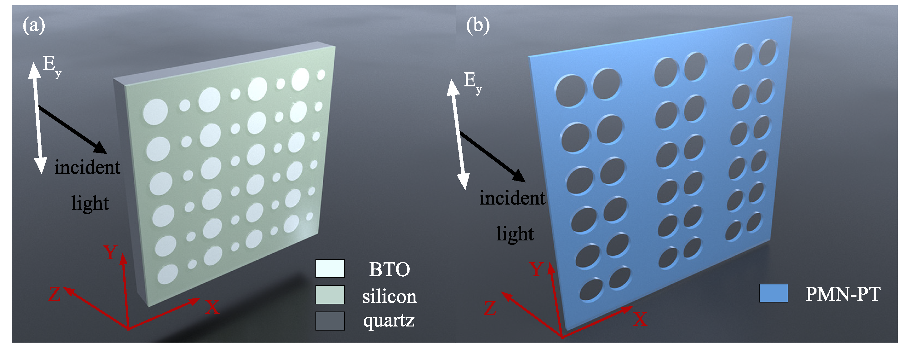
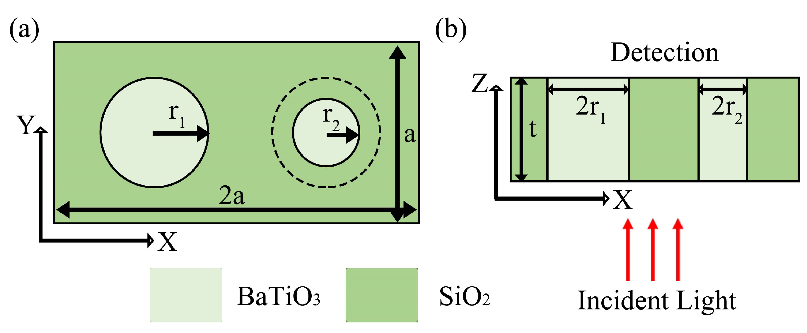
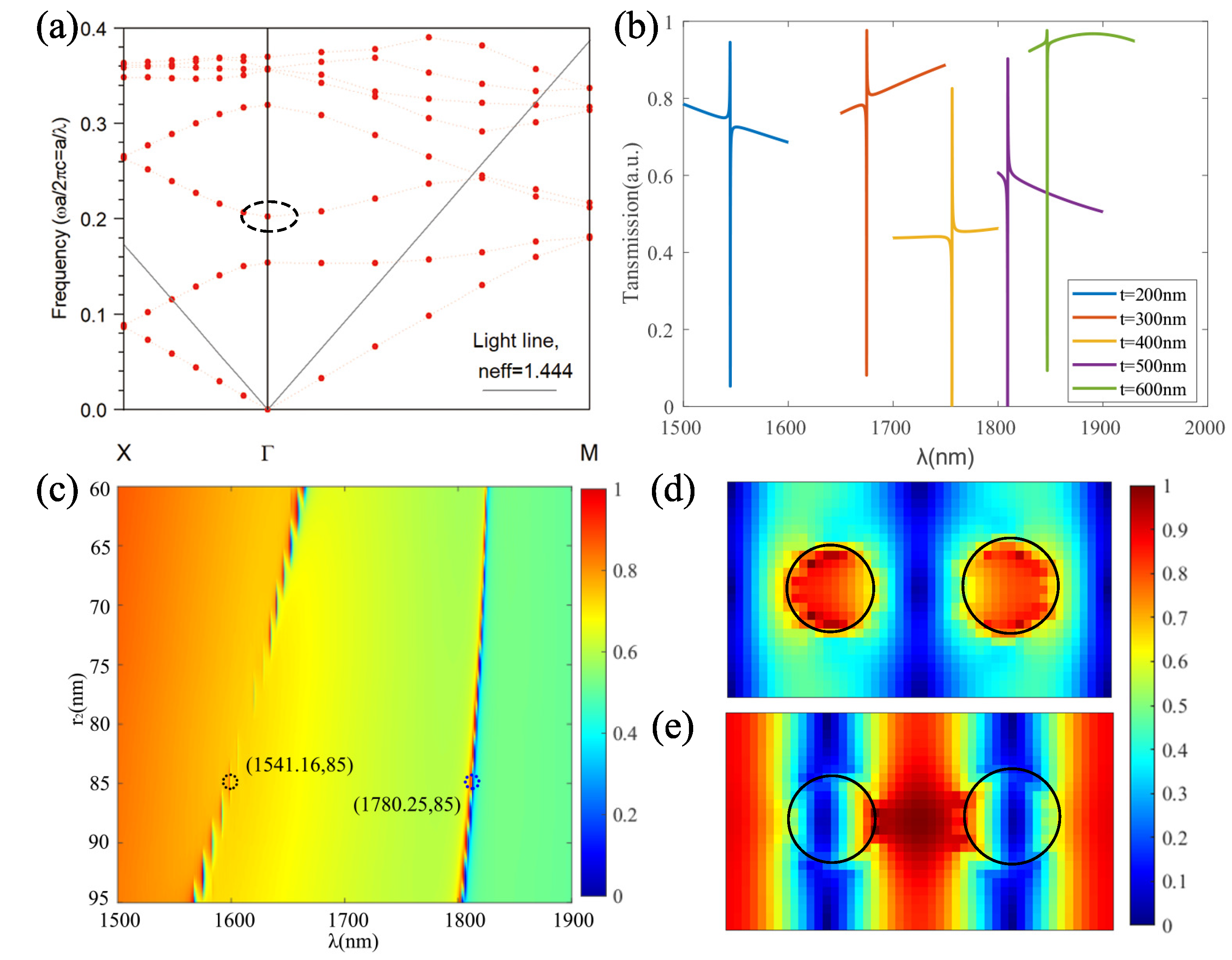
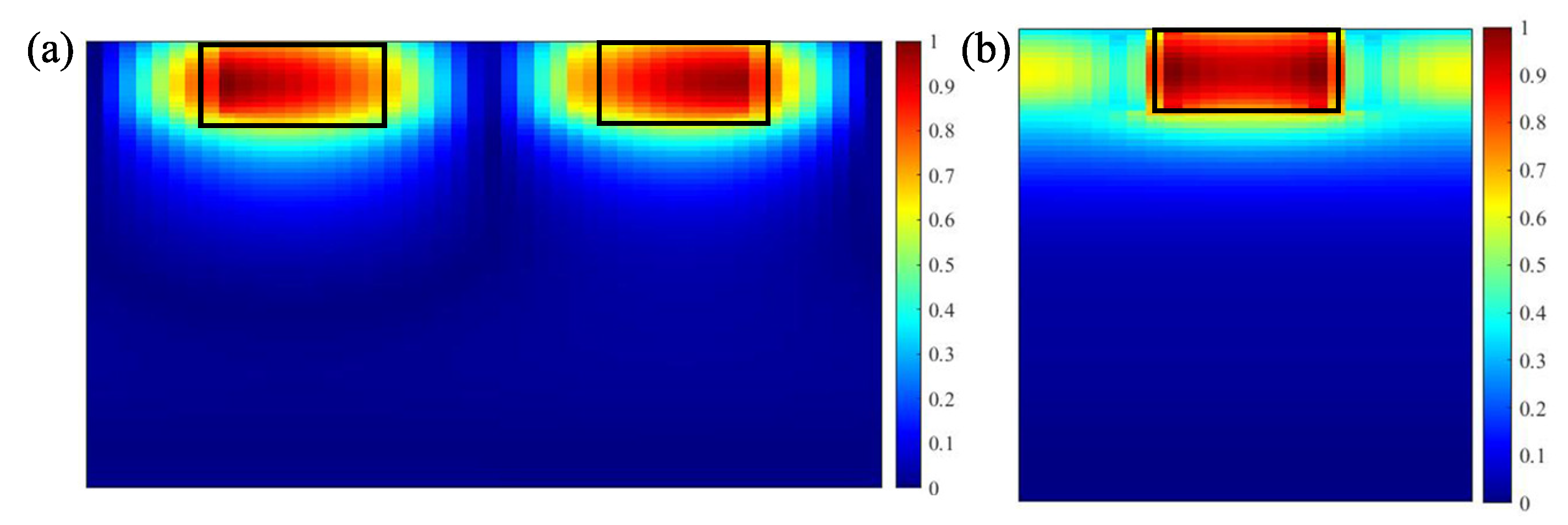
2.1. E-Field Sensor Based on BTO

The 3D BTO based nanostructure is shown in Figure 1a, and the different 2D cross sections are shown in Figure 2. Here, the refractive index of BTO is considered as 1.6 and the silicon is considered as 3.48. The XY-cross section is shown in Figure 2a which is a unit cell of two dimensional BTO based nanostructure employed in dispersion diagram modeling. The size of the rectangle is labeled as 2a×a. In order to generate Fano resonance at normally incident light, the symmetry of the rectangular structure is broken by scaling the hole radius. The two BTO holes radius are labeled as r 1 and r 2 and the scaling factor r a s c a l is defined as r a s c a l = r 1 / r 2 . The XZ-cross section of the structure is shown in Figure 2b where the silicon slab thickness t is labeled. The PWE method from the commercial software Rsoft BANDSOLVE is employed for dispersion diagram modeling. In general, low group velocity eigen mode and flat band is favored because it facilitates a high Q resonance. The aim is to find the appropriate filling ratio r a (defined as r 1 /a) and asymmetric hole radius scaling factor r a s c a l which allows a slow mode located in the Γ -point above the light line. However, slow light mode tends to be more likely to occur at edge points in the dispersion diagram. The broken symmetry of the rectangular lattice will band fold the edge slow mode to the left of the Brillouin zone.
As shown in Figure 3a, the solution of y-polarized eigen slow mode with the following parameter r a = 0.225 and r a s c a l = 1.1 is the optimized results and the mode is circled out which lies at the normalized frequency of a/ λ = 0.2. By putting the operating wavelength around 1550 nm in order to compatible with most telecommunication equipment, therefore the corresponding lattice constant is a = 310 nm. From the parameter determined by PWE calculations i.e., r a = 0.225, r a s c a l = 1.1, assuming the silicon slab thickness t = 200 nm and vary a between 310 to 360 nm, 3D-FDTD is employed to model the normalized transmission spectra of the unit cell structure with finite thickness, where the transmission is normalized by the maximum. A larger period a will red shift the resonance and when a = 350 nm, the resonance is located at the vicinity of 1550 nm.
Next, studies of how the resonance varies with respect to the thickness of thin film silicon t while fixing other parameters such as a = 350 nm, the radius of one circular holes is fixed at r 1 = 80 nm, r 2 = 85 nm are carried out. The calculated transmission is shown in Figure 3b and from which one can see that the resonance wavelength is red shifted with the increasing of the thickness t, but the resonance Q is decreasing. Therefore, the thickness of silicon slab is chosen t = 200 nm. By fixing parameters of a = 350 nm, t = 200 nm, r 1 = 80 nm, a study of varying r a s c a l , which is related to the degree of asymmetry, is carried out. The result is shown in Figure 3c, from which can see two resonance peaks one located around 1550 nm and the other around 1780 nm.
As the r a s c a l approaching to 1 i.e., the difference between the radius of two circular holes becomes smaller, a sharper resonance peak corresponding to a higher Q is achieved. If the r a s c a l = 1 i.e., the structure becomes a square lattice, then the Fano resonance will not able to observe in the transmission spectrum. This is because the Q of the corresponding mode is infinite with symmetrical structures. A continuous wave excitation at different resonance wavelength for r 2 = 85 nm is carried in order to obtain the field distributions. Figure 3d shows the normalized electric field distribution corresponding to r 2 = 85 nm which is defined as E = ( E i E m i n ) / ( E m a x E m i n ) , the resonance wavelength λ r e s = 1541.16 nm which is circled out in Figure 3c as black dotted circle. And Figure 3d shows the normalized electric field distribution at the resonance wavelength λ r e s = 1780.25 nm which is circled out in Figure 3c as blue dotted circle. One can see that the electric field around 1550 nm is mostly localized in BTO material from Figure 3d, and the electric field of the resonance peak around 1780 nm is mostly localized in thin film silicon in Figure 3e.
The elecric field distribution at λ r e s = 1541.16 nm for XZ and YZ are shown in Figure 4. Figure 4a is the XZ section through the left of the circle and Figure 4b is the YZ section through the left of the circle r 1 = 80 nm. It can be clearly seen that the electric field is well localized in BTO.
In fact, the above result is in consistent with the dispersion diagram modelling. The mode property with the electric field mostly confined in the air holes corresponds to air mode in the dispersion diagram while the neighbor mode corresponds to a dielectric mode with the electric field mostly confined in the dielectric slab. In order to exploit the EO effect of BTO here, a mode which allows confining light in the material is chosen. An enhancement factor f o p t is employed to the quantify the optical electric field localization capability. It’s defined as the ratio between volume integration of the electric field amplitude in all the EO material regions of nanostructure and the volume integration of the electric field amplitude in the same region but without the nanostructure:
f o p t = s t r u c t u r e d | E ( x , y , z ) | d x d y d z n o n s t r u c t u r e d | E ( x , y , z ) | d x d y d z
Table 1 summarizes the variation of the enhancement factor f o p t and quality factor Q versus different r 2 , i.e., asymmetric degree, while other parameters are fixed at a = 350 nm, r 1 = 80 nm, t = 200 nm. It can be seen that a high Q can lead to a large f o p t , which results in a potentially high effective EO effect.
From the above optimization, the chosen optimal structural parameters of E-field sensor based on BTO are a = 350 nm, r 1 = 80 nm, r 2 = 85 nm, t = 200 nm, which will be used for analysis in next section.

2.2. Sensitivity Analysis Based on BTO

Thin film BTO generally can be achieved via molecular beam epitaxy (MBE) [24] and bottom-up synthesis [25]. The reported EO coefficient of the MBE growth thin film reachs up to γ = 148 pm/V [24]. However, the MBE growth film is an expensive process and it is not compatible to any substrate. The reported EO coefficient of the bottom-up synthesis BTO nanoparticle is about γ = 37.04 pm/V [17], which is lower than the MBE growth film but is comparable to LN. In addition, the BTO particle based film can be spin coated on any type of substrate. Here the chosen BTO is based on nanoparticles which the refractive index is considered at 1.6 because of considering the duty rate of air in the BTO holes. Therefore the BTO nanoparticle effective EO coefficient of γ = 37.04 pm/V is employed for the sensitivity analysis of BTO based nanostructure E-field sensor.
The principle of EO based E-field sensor is the EO effect where the presence of applied electric field in EO material will result in a change of the refractive index of EO materials. Assuming the EO effect is along the z-axis, then the index variation is as follows:
Δ n = 1 2 n 3 γ E z
where the γ is the EO coefficient and E z is the applied E-field amplitude.
The nanopatterned structure will confine the electric field in the EO material and it is quantified by the enhancement factor f o p t , therefore the effective induced EO effect will be enhanced. The Pockels effect which takes into account the nanostructure induced field enhancement is as follows [26]:
Δ n = 1 2 n 3 γ e f f E z f o p t 2
The sensitivity is evaluated by substituting different field amplitude to be measured into Equation (3), and then a 3D-FDTD simulation of the structure with EO effect induce Δ n is performed. Under applied E-field amplitude of 1 × 10 5 V/m, the result is shown in Figure 5a. From Figure 5a one can see that the resonance wavelength λ r e s red shifts 11.6 nm with the applied electric field E z = 1 × 10 5 V/m and a decrease in the resonance extinction ratio.
Here, the wavelength interrogation method is employed for the E-field sensing. How the resonance wavelength shift versus applied electric field is carried out in Figure 5b, from which one can see that the λ r e s varies quasi-linearly with E z which is desired for sensing application. By fitting the linear equation of the resonance wavelength and the amplitude of the applied electric field as λ r e s = 0.1213 × 10 3 E z + 1541.16 . The slope of the fitted equation represents the sensitivity of the E-field sensor that the sensitivity is defined as
S = Δ λ r e s E z
where the Δ λ r e s is the magnitude of resonance wavelength drifts. Therefore the average sensitivity is at S a v g = 0.1213 pm/(V/m).
The minimum detectable electric field of the E-field sensor E m i n is evaluated depending on the ability of wavelength drift Δ λ r e s and the resolution of the optical spectrum analyzer. According to S a v g = 0.1213 pm/(V/m), E m i n = 0.82 V/m can be obtained if an optical spectrum analyzer is used for detection whose resolution is 0.1 pm.

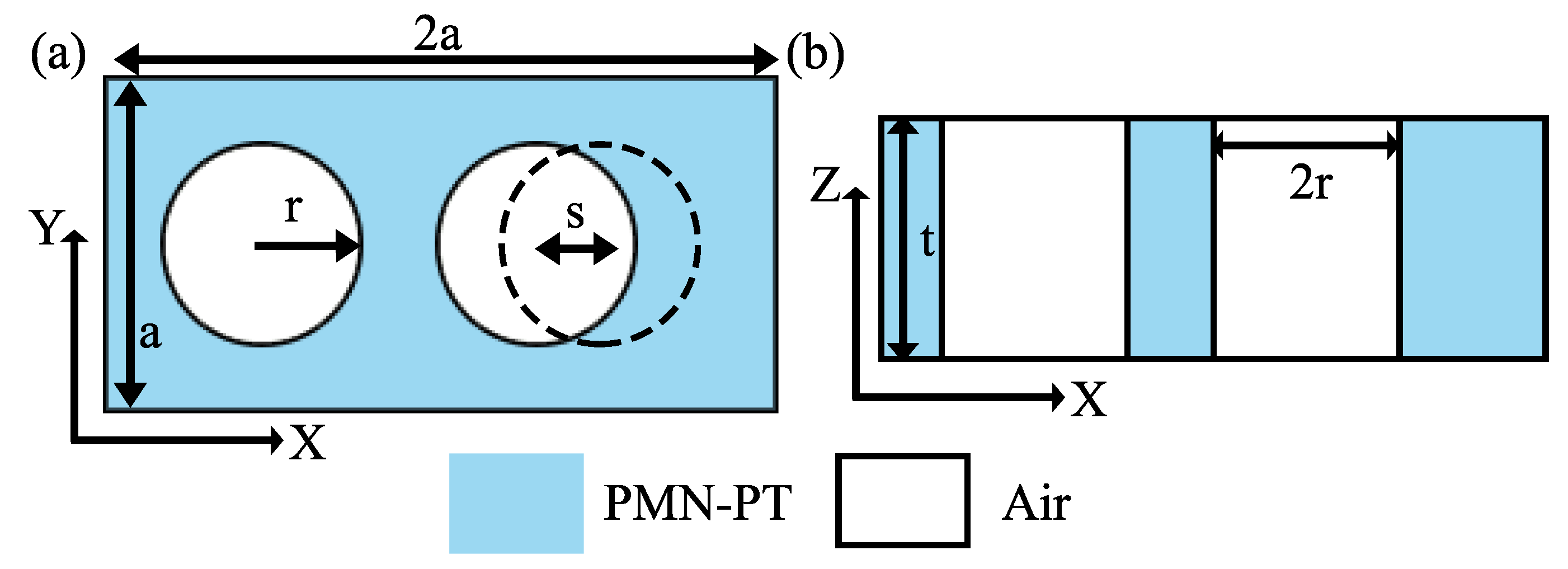
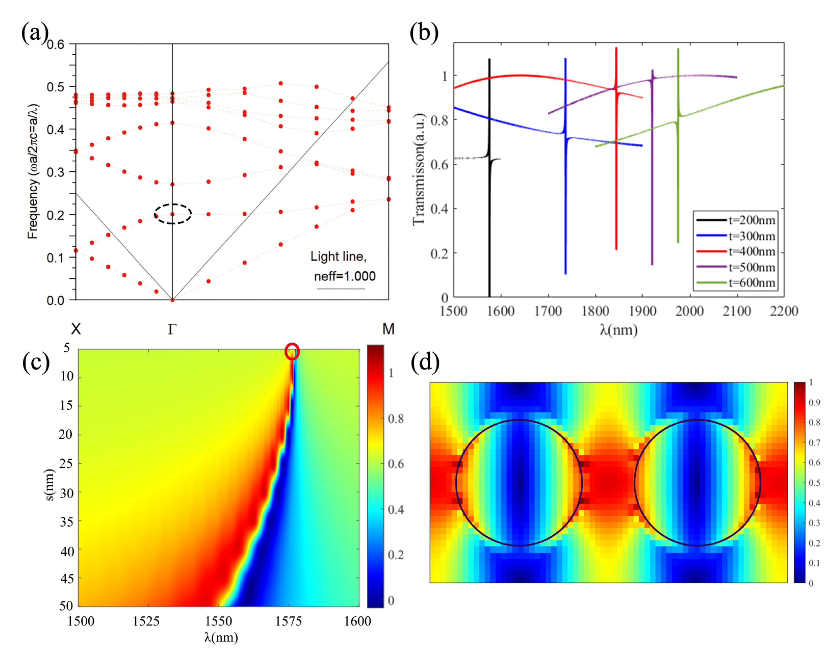
2.3. E-Field Sensor Based on PMN-PT

2D profiles of PMN-PT based nanostructure is shown in Figure 6. The unit cell of the structure is a rectangle lattice whose size is 2a×a in XY plane as labeled in Figure 6a. Broken structure symmetry is employed to bandfold bandedge slow mode to the Γ -point of Brillouin zone which is the same principle as the above structure designed in BTO based E-field sensor. The asymmetricity is obtain here via offsetting s to one air holes left. The XZ-cross section of the structure, where the thickness of thin film PMN-PT of t is considered in the 3D simulation, is shown in Figure 6b. Here, the refractive index of PMN-PT is taken as 2.65 [27].
The dispersion band curve simulation of PMN-PT rectangular lattice versus different duty rate r a ( r a = r / a ) and the percentage of offset o f f X r a is carried out where o f f X r a is defined as s = a × o f f X r a . Tuning the structure parameter is aim to find a mode located in the Γ -point above the light line with slow group velocity or flat band character. The optimized result is shown in Figure 7a. It corresponds y-polarized incident light and the structure parameters are of r a = 0.3 and o f f X r a = 0.01. The chosen mode is circled out in black dotted circle which lies at the normalized frequency of a/ λ = 0.2. By determining the working wavelength at 1550 nm, then the mode at a/ λ = 0.2 will lead to a lattice constant a = 310 nm. Next, 3D-FDTD simulations of PMN-PT based nanostructure varying a between 310 nm to 500 nm while a fixed thin film PMN-PT thickness t = 200 nm are carried out. The result shows that when a = 480 nm, the resonance is located at the vicinity of 1550 nm.
Then simulations of varying the thickness of thin film PMN-PT t while fixed parameters of lattice constant a = 480 nm, r = 175 nm, s = 5 nm are carried out. The result is shown in Figure 7b, from which one can see that with the increasing thickness t, the resonance wavelength red shifts. The corresponding resonance Q and enhancement factor f o p t are also calculated and it decreases with the increase of the thickness of t. Therefore, the thickness of thin film PMN-PT is as t = 200 nm.
Next a study of fine tuning the offset value s is carried out and the transmission spectrum versus s from 5 nm to 50 nm is shown in Figure 7c. It can seen that the resonance peak red shifts and the peak becomes steeper when reducing the offset s. The corresponding resonance Q and enhancement factor f o p t are calculated and it is summarized in Table 2. With the offset value s = 5 nm which corresponds to red circled out in Figure 7c, the resonance Q can reach up to 9.27 × 10 3 and a large f o p t of 95.8 is obtained. The normalized electric field corresponding to the red circled out mode in Figure 7c is carried out in Figure 7d which shows that the electric field is mostly localized in the PMN-PT material. The elecric field distribution for XZ and YZ are carried out in Figure 8, both sections are through the left of the circle. As seen in Figure 8, the electric field is localized in PMN-PT to enhance the effective EO coefficient.
The chosen optimal structural parameters of PMN-PT based E-field sensor are a = 480 nm, r = 175 nm, s = 5 nm, t = 200 nm. Next section will discuss the sensitivity with this optimal parameters.

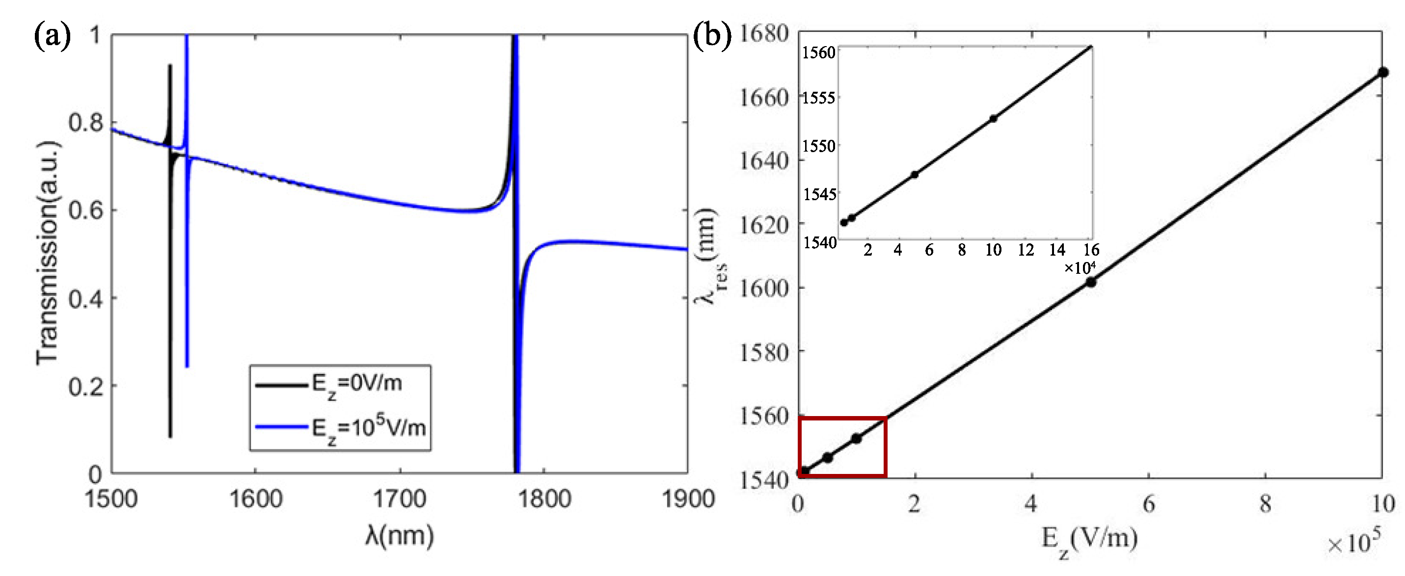
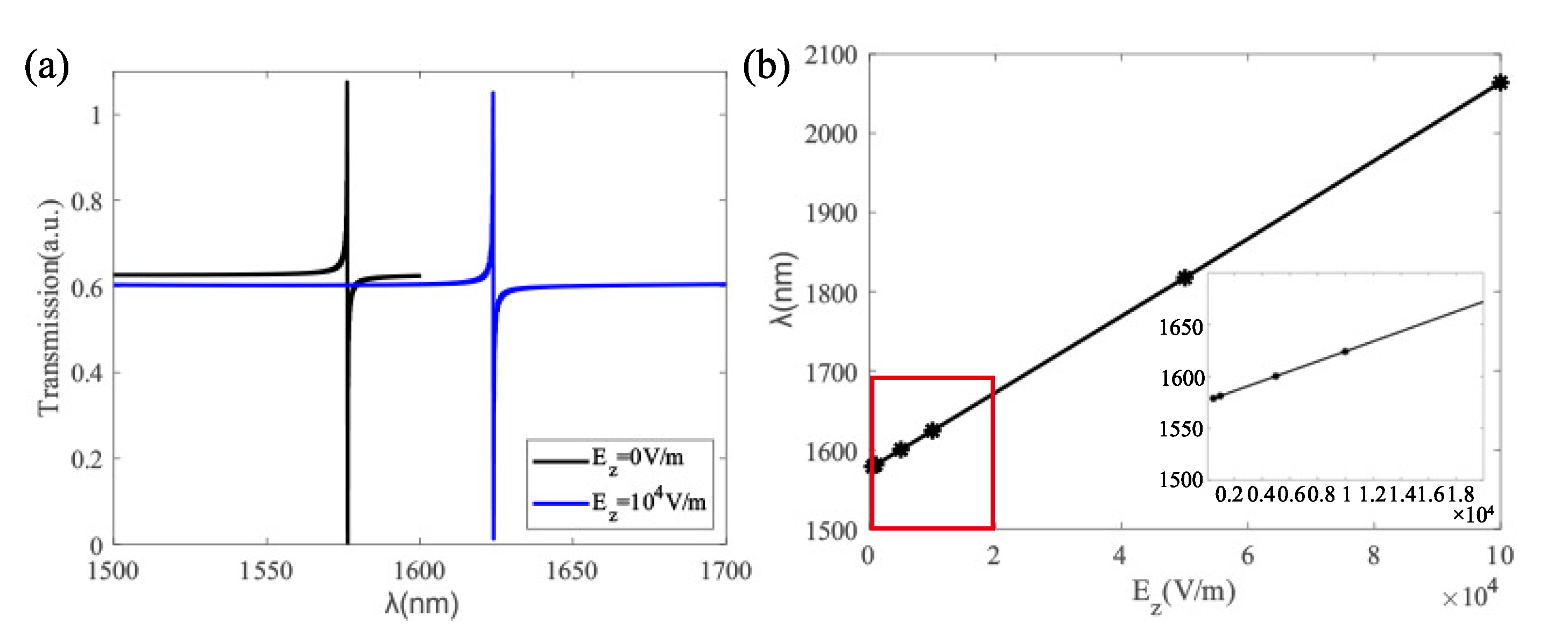
2.4. Sensitivity Analysis Based on PMN-PT

In terms of the EO coefficient of PMN-PT, there are different reported value ranging from several tens of pm/V up to several hundred pm/V due to the different crystalline growth and poling process [18,28]. Here, a (111)-oriented rhombohedral phase 0.67PMN-0.33PT, which is relatively commonly exploited in the literature, is chosen around 2.7 [19]. According to the Sellmeier equation [27] that refractive index is 2.65 at 1550 nm and the reported EO coefficient is 112 pm/V [29] at 633 nm. Note that, simulations performed here only take into account the extraordinary index since only y-polarized light is considered here. The enhancement factor f o p t of 95.8 is achieved for the PMN-PT optimal structure with parameters of a = 480 nm, r = 175 nm, s = 5 nm, t = 200 nm. According to the Equation (3), a higher enhancement factor f o p t results in a higher refractive index variation, so that can increase the effective EO effect.
3D-FDTD simulations with the refractive index of PMN-PT varied by Equation (3) and by applying different external electric field are carried out. The transmission spectra of no applied E-field and 10 4 V/m E-field are shown in Figure 9a, and it shows that the resonance peak wavelength red shifts nearly 48 nm and the sensitivity S is calculated to be 4.768 pm/(V/m).
How the resonance wavelength changes versus different amplitude of the applied electric field is plotted in Figure 9b. The dots are the simulation data and the linear fitting curve is λ r e s = 4.774 × 10 3 E z + 1576.42 . The slope of the curve which is 4.774 pm/(V/m) represents the average resonance wavelength shift sensitivity. Notes that, the magnitude of the sensitivity is around four times higher than that of the same geometry but replacing PMN-PT into LN [15]. By considering an optical spectrum analyzer with a resolution of about 0.1 pm, then, the minimum detectable electric field E m i n of (111) oriented rhombohedral phase 0.67PMN-0.33PT based E-field sensor is calculated to be 20 mV/m.

3. Discussion on the Sensitivity and Possible Fabrication Method

The above simulation presents two EO materials (BTO nanoparticles and PMN-PT thin film) combined with different nanostructures design to generate Fano resonance via rectangular lattice geometry. The nanostructure can localize the electric field on EO material, and the optical field enhancement factors f o p t reach up to 105 for BTO and around 96 for PMN-PT, respectively. The optimized geometry allows to achieve a sensitivity of 0.1213 pm/(V/m) for BTO and 4.774 pm/(V/m) for PMN-PT. If an optical spectrum analyzer with resolution of 0.1 pm is considered, then the minimum detectable field is 0.82 V/m for BTO and 20 mV/m for PMN-PT.
As seen in Figure 10, the hole radius and hole position shift value have different effect on the value of resonance Q for BTO and PMN-PT nanostructure. In terms of BTO nanostructure, radius is the key parameter. As can be seen in Figure 10a, the Q value is quite robust around radius r 2 value of 75 nm to 85 nm where the Q value degrade only down to 83% of the peak value. However, in terms of PMN-PT based nanostructure, the resonance Q value decreases sharply with the increase of the s value, i.e., the asymmetric. As can be seen in Figure 10b, when s changes from 5 nm to 10 nm, Q value will quickly drop to about 1700 down to 17% of its value at s = 5 nm.
The simulation reveals that PMN-PT based nanostructure yields a better sensitivity. The E-field sensitivity is affected by two parts, one is the influence of the EO effect, i.e., quantified by Equation (3). The other is the resonance wavelength shift versus unit index variation. The latter one is related to the group velocity of the mode which here is optimized via PWE band diagram simulations. Here the high sensitivity of PMN-PT nanostructure is mainly due to a larger EO effect. It has a refractive index of around 2.65 and the effective EO coefficient γ e f f = 112 pm/V and the optimized structure yields a field enhancement factor f o p t of around 96. The effective EO coefficient of PMN-PT material has different values ranging from several tens pm/V up to several hundreds pm/V due to the different material growth and processing [19]. The effective EO coefficient γ e f f = 112 pm/V employed here can be achieved via (111) oriented rhombohedral phase PMN-PT [29].
As to the possible fabrication of the BTO nanostructure, BTO nano particle with tetragonal phase is chosen since it can avoid the mechanical unstable property of bulk BTO. The BTO based structure can benefit from the mature silicon photonics device fabrication and the BTO nanoparticles can be spin coated to fill the air holes in patterned silicon [21]. The refractive index considered here is 1.6 which is smaller than bulk BTO (around 2.4), since nanoparticles based structure is not 100% densely packed. The effective EO coefficient γ e f f of 37 pm/V is considered which is an averaged value for the reported BTO based nanoparticles [17].
PMN-PT is a relatively new material for optical device, but nanostructures such as nanobelts [30], nanowires [31] and nanorod [32] have been demonstrated for piezoelectronic transistor (PET) applications. Different materials poling (for instance A.C. and D.C.) will lead to different electro-optical coefficients and the transmittance of electro-optical crystals [33], i.e., the transmittance of conventional D.C. poled PMN-PT is lower than that of A.C. poled PMN-PT. Therefore, PMN-PT may be able to make EO devices with higher performance. With the advances in crystal growth, PMN-PT might be a good optical material for EO based devices.
In terms material, the two investigated EO materials have different reported EO coefficient depending on the crystalline orientation, crystal phase, polling condition [33] and growth conditions [34]. This means that for the novel EO materials, the same material can be used to obtain higher EO coefficients depending on physical properties and processing to design more sensitive EO devices.
Table 3 compares the states of the art E-field sensor with different structures, parameters such as footprint size, quality factor Q, sensitivity S and the minimum detectable electric field E m i n are listed. The presented E-field sensor based on BTO and PMN-PT achieve the highest sensitivities as shown in bold size among others. In addition, in terms of the spatial resolution, the film presented here is only 200 nm which could yield a high resolution in this direction. In conclude, modes with slow group velocity and high Q property is demonstrated for highly sensitive E-field measurement, pushing the measurement limits towards weak electric fields.

Author Contributions

Conceptualization, software development, and original draft preparation were done by X.Y., H.L. and H.G.; F.L. and C.L. conceived and supervised the project; Reviewing and editing by W.Q.; Calculations and analyzes of results by X.Y. and W.Q. All authors have read and agreed to the published version of the manuscript.

Funding

This research was funded by the National Natural Science Foundation of China (61775084, 62075088), the NSAF (U2030103), the Natural Science Foundation of Guangdong Province (2020A1515).

Institutional Review Board Statement

Not applicable.

Informed Consent Statement

Not applicable.

Data Availability Statement

The data that support the findings of this study are available from the corresponding author upon reasonable request.

Conflicts of Interest

The authors declare no conflict of interest.

References

  1. Steinecke, T.; Bischoff, M.; Brandl, F.; Hermann, C.; Klotz, F.; Mueller, F.; Pfaff, W.; Unger, M. Generic IC EMC test specification. In Proceedings of the 2012 Asia-Pacific Symposium on Electromagnetic Compatibility, Singapore, 21–24 May 2012; IEEE: Piscataway, NJ, USA, 2012; pp. 5–8. [Google Scholar]
  2. Klotz, F. EMC test specification for integrated circuits. In Proceedings of the 2007 18th International Zurich Symposium on Electromagnetic Compatibility, Munich, Germany, 24–28 September 2007; IEEE: Piscataway, NJ, USA, 2007; pp. 73–78. [Google Scholar]
  3. Burford, N.M.; El-Shenawee, M.O. Review of terahertz photoconductive antenna technology. Opt. Eng. 2017, 56, 010901. [Google Scholar] [CrossRef]
  4. Zhang, W.; Li, P.; Zhou, N.; Suo, C.; Chen, W.; Wang, Y.; Zhao, J.; Li, Y. Method for localization aerial target in AC electric field based on sensor circular array. Sensors 2020, 20, 1585. [Google Scholar] [CrossRef] [Green Version]
  5. Saniour, I. Exploitation des Effets Électro-Optiques Pour la Sécurité en IRM: Applications des Liaisons Optiques Pour des Capteurs RF Endoluminaux et des Sondes de Mesure du TAS. Ph.D. Thesis, Université de Lyon, Lyon, France, 2017. [Google Scholar]
  6. Nastuta, A.V.; Gerling, T. Cold Atmospheric Pressure Plasma Jet Operated in Ar and He: From Basic Plasma Properties to Vacuum Ultraviolet, Electric Field and Safety Thresholds Measurements in Plasma Medicine. Appl. Sci. 2022, 12, 644. [Google Scholar] [CrossRef]
  7. Joseph, W.; Martens, L. The influence of the measurement probe on the evaluation of electromagnetic fields. IEEE Trans. Electromagn. Compat. 2003, 45, 339–349. [Google Scholar] [CrossRef]
  8. Kanda, M. Standard antennas for electromagnetic interference measurements and methods to calibrate them. IEEE Trans. Electromagn. Compat. 1994, 36, 261–273. [Google Scholar] [CrossRef]
  9. Yan, Z.; Liu, W.; Wang, J.; Su, D.; Yan, X.; Fan, J. Noncontact wideband current probes with high sensitivity and spatial resolution for noise location on PCB. IEEE Trans. Instrum. Meas. 2018, 67, 2881–2891. [Google Scholar] [CrossRef]
  10. Hsu, L.; Baida, F.I.; Ndao, A. Local field enhancement using a photonic-plasmonic nanostructure. Opt. Express 2021, 29, 1102–1108. [Google Scholar] [CrossRef] [PubMed]
  11. Zhang, J.; Luo, C.; Zhao, Z. Design and application of integrated optics sensor for measurement of intense pulsed electric field. J. Light. Technol. 2019, 37, 1440–1448. [Google Scholar] [CrossRef]
  12. Calero, V.; Suarez, M.A.; Salut, R.; Baida, F.; Caspar, A.; Behague, F.; Courjal, N.; Galtier, L.; Gillette, L.; Duvillaret, L.; et al. An ultra wideband-high spatial resolution-compact electric field sensor based on Lab-on-Fiber technology. Sci. Rep. 2019, 9, 8058. [Google Scholar] [CrossRef] [PubMed] [Green Version]
  13. Hoblos, A.; Suarez, M.; Courjal, N.; Bernal, M.P.; Baida, F.I. Excitation of symmetry protected modes in a lithium niobate membrane photonic crystal for sensing applications. OSA Contin. 2020, 3, 3008–3018. [Google Scholar] [CrossRef]
  14. Benea-Chelmus, I.C.; Salamin, Y.; Settembrini, F.F.; Fedoryshyn, Y.; Heni, W.; Elder, D.L.; Dalton, L.R.; Leuthold, J.; Faist, J. Electro-optic interface for ultrasensitive intracavity electric field measurements at microwave and terahertz frequencies. Optica 2020, 7, 498–505. [Google Scholar] [CrossRef]
  15. Qiu, W.; Ndao, A.; Lu, H.; Bernal, M.P.; Baida, F.I. Guided resonances on lithium niobate for extremely small electric field detection investigated by accurate sensitivity analysis. Opt. Express 2016, 24, 20196–20209. [Google Scholar] [CrossRef]
  16. Abel, S.; Eltes, F.; Ortmann, J.E.; Messner, A.; Castera, P.; Wagner, T.; Urbonas, D.; Rosa, A.; Gutierrez, A.M.; Tulli, D.; et al. Large Pockels effect in micro-and nanostructured barium titanate integrated on silicon. Nat. Mater. 2019, 18, 42–47. [Google Scholar] [CrossRef]
  17. Karvounis, A.; Vogler-Neuling, V.V.; Richter, F.U.; Dénervaud, E.; Timofeeva, M.; Grange, R. Electro-Optic Metasurfaces Based on Barium Titanate Nanoparticle Films. Adv. Opt. Mater. 2020, 8, 2000623. [Google Scholar] [CrossRef]
  18. Jeong, D.Y.; Lu, Y.; Sharma, V.; Zhang, Q.; Luo, H.S. Linear electrooptic properties of Pb(Mg1/3Nb2/3)O3-PbTiO3 single crystals at compositions near the morphotropic phase boundary. Jpn. J. Appl. Phys. 2003, 42, 4387. [Google Scholar] [CrossRef]
  19. Song, H.C.; Ha, J.Y.; Kim, J.S.; Yoon, S.J.; Jeong, D.Y. Temperature Dependences of Piezoelectric and Linear Electrooptic Properties of Rhombohedral 0.67Pb(Mg1/3Nb2/3)O3-0.33PbTiO3 Single Crystal Oriented in <111> Direction. Jpn. J. Appl. Phys. 2007, 46, 1540. [Google Scholar]
  20. Baek, S.H.; Eom, C.B. Epitaxial integration of perovskite-based multifunctional oxides on silicon. Acta Mater. 2013, 61, 2734–2750. [Google Scholar] [CrossRef]
  21. Di, X. Fabrication and Characterisation of Epitaxial PMN-PT Nano-Structures. Ph.D. Thesis, Swiss Federal Institute of Technology Lausanne (EPFL), Lausanne, Switzerland, 2019. [Google Scholar]
  22. Wang, C.; Zhang, M.; Chen, X.; Bertrand, M.; Shams-Ansari, A.; Chandrasekhar, S.; Winzer, P.; Lončar, M. Integrated lithium niobate electro-optic modulators operating at CMOS-compatible voltages. Nature 2018, 562, 101–104. [Google Scholar] [CrossRef] [PubMed]
  23. Reiss, S.; Bitzer, A.; Bock, M. An optical setup for electric field measurements in MRI with high spatial resolution. Phys. Med. Biol. 2015, 60, 4355. [Google Scholar] [CrossRef]
  24. Abel, S.; Stöferle, T.; Marchiori, C.; Rossel, C.; Rossell, M.D.; Erni, R.; Caimi, D.; Sousa, M.; Chelnokov, A.; Offrein, B.J.; et al. A strong electro-optically active lead-free ferroelectric integrated on silicon. Nat. Commun. 2013, 4, 1671. [Google Scholar] [CrossRef] [PubMed] [Green Version]
  25. Karvounis, A.; Timpu, F.; Vogler-Neuling, V.V.; Savo, R.; Grange, R. Barium titanate nanostructures and thin films for photonics. Adv. Opt. Mater. 2020, 8, 2001249. [Google Scholar] [CrossRef]
  26. Qiu, W.; Ndao, A.; Vila, V.C.; Salut, R.; Courjal, N.; Baida, F.I.; Bernal, M.P. Fano resonance-based highly sensitive, compact temperature sensor on thin film lithium niobate. Opt. Lett. 2016, 41, 1106–1109. [Google Scholar] [CrossRef] [PubMed]
  27. Wan, X.; Chan, H.; Choy, C.; Zhao, X.; Luo, H. Optical properties of (1-x)Pb(Mg1/3Nb2/3)O3-xPbTiO3 single crystals studied by spectroscopic ellipsometry. J. Appl. Phys. 2004, 96, 1387–1391. [Google Scholar] [CrossRef]
  28. Wan, X.; Luo, H.; Zhao, X.; Wang, D.; Chan, H.; Choy, C. Refractive indices and linear electro-optic properties of (1-x)Pb(Mg1/3Nb2/3)O3-xPbTiO3 single crystals. Appl. Phys. Lett. 2004, 85, 5233–5235. [Google Scholar] [CrossRef] [Green Version]
  29. Hu, Q.; Yang, R.; Zhao, Y.; Zhao, W.; Liu, X.; Fu, X.; Luan, P.; Song, K.; Zhuang, Y.; Xu, Z.; et al. Achieve single domain state in (111)-oriented rhombohedral phase PMN-PT relaxor ferroelectric single crystals for electro-optical application. Appl. Phys. Lett. 2019, 115, 222901. [Google Scholar] [CrossRef]
  30. Chen, Y.; Zhang, Y.; Zhang, L.; Ding, F.; Schmidt, O.G. Scalable single crystalline PMN-PT nanobelts sculpted from bulk for energy harvesting. Nano Energy 2017, 31, 239–246. [Google Scholar] [CrossRef]
  31. Moorthy, B.; Baek, C.; Wang, J.E.; Jeong, C.K.; Moon, S.; Park, K.I.; Kim, D.K. Piezoelectric energy harvesting from a PMN-PT single nanowire. RSC Adv. 2017, 7, 260–265. [Google Scholar] [CrossRef] [Green Version]
  32. Li, C.; Liu, X.; Luo, W.; Xu, D.; He, K. Surfactant-assisted hydrothermal synthesis of PMN-PT nanorods. Nanoscale Res. Lett. 2016, 11, 49. [Google Scholar] [CrossRef] [Green Version]
  33. Qiu, C.; Wang, B.; Zhang, N.; Zhang, S.; Liu, J.; Walker, D.; Wang, Y.; Tian, H.; Shrout, T.R.; Xu, Z.; et al. Transparent ferroelectric crystals with ultrahigh piezoelectricity. Nature 2020, 577, 350–354. [Google Scholar] [CrossRef] [PubMed]
  34. Kormondy, K.J.; Abel, S.; Fallegger, F.; Popoff, Y.; Ponath, P.; Posadas, A.B.; Sousa, M.; Caimi, D.; Siegwart, H.; Uccelli, E.; et al. Analysis of the Pockels effect in ferroelectric barium titanate thin films on Si (0 0 1). Microelectron. Eng. 2015, 147, 215–218. [Google Scholar] [CrossRef] [Green Version]
  35. Rajasekar, R.; Robinson, S. Nano-electric field sensor based on two dimensional photonic crystal resonator. Opt. Mater. 2018, 85, 474–482. [Google Scholar] [CrossRef]
  36. Ma, X.; Zhuang, C.; Zeng, R.; Zhou, W. Large-dynamic-range athermal lithium niobite on insulator/TiO2 nanobeam electric field sensor. J. Phys. D Appl. Phys. 2020, 54, 105101. [Google Scholar] [CrossRef]
  37. Goncharenko, I.; Ryabtsev, V.N. High-frequency electric field intensity sensor based on double-slot waveguides filled with electro-optical polymer. Quantum Electron. 2021, 51, 1044. [Google Scholar] [CrossRef]
  38. Li, J.; Xia, Z.; Liu, L.; Zhang, L.; Bian, Z.; Hu, A.; Chu, F. Performance analysis of multifunctional SPR sensor based on electro-optic crystal. Photonics Nanostruct. 2020, 42, 100838. [Google Scholar] [CrossRef]
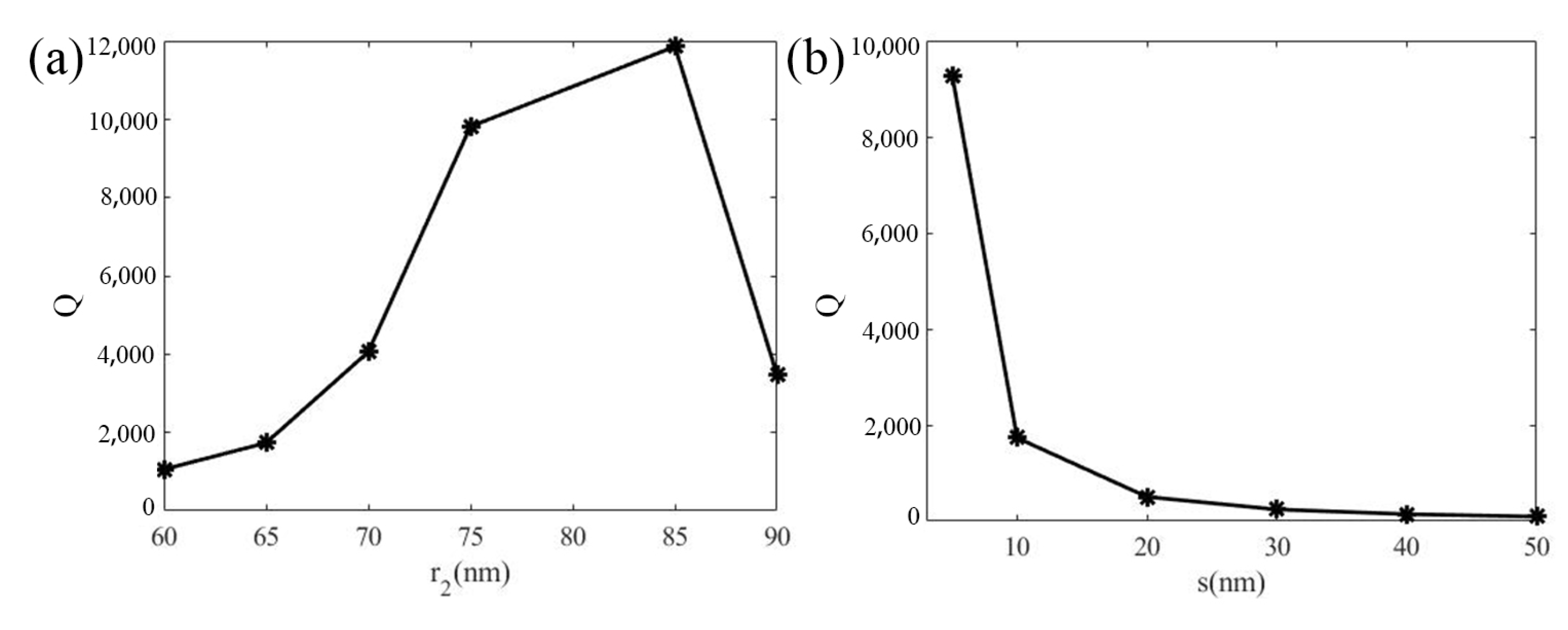
Figure 1. (a) A sketch of the proposed E-field sensor based on nano-patterned thin film silicon on quartz where the air holes are filled with BTO nanoparticles. (b) A schematic of the proposed E-field sensor which is made of nano-patterned free standing PMN-PT thin film.
Photonics 09 00431 g001
Figure 2. (a) 2D plane diagram of a BTO rectangle unit cell in XY plane. (b) 2D plane diagram of a BTO rectangle unit cell in XZ plane.
Photonics 09 00431 g002
Figure 3. (a) Band diagram for rectangular structure with parameters values r a = 0.225, r a s c a l = 1.1. (b) Normalized transmission spectra for a = 350 nm, r 1 = 80 nm, r 2 = 85 nm, varying t. (c) Normalized transmission spectra for a = 350 nm, t = 200 nm, r 1 = 80 nm, varying r 2 . The wavelength of black dotted circle is 1541.16 nm and the wavelength of blue dotted circle is 1780.25 nm, respectively in r 2 = 85 nm. (d) Normalized electric field distribution at 1541.16 nm. (e) Normalized electric field distribution at 1780.25 nm.
Photonics 09 00431 g003
Figure 4. Normalized electric field distribution at 1541.16 nm for (a) XZ and (b) YZ.
Photonics 09 00431 g004
Figure 5. (a) Normalized transmission spectrum with applied electric field of E z = 10 5 V/m and without applied electric field in parameter a = 350 nm, r 1 = 80 nm, r 2 = 85 nm, t = 200 nm. (b) Variation of resonance wavelength λ r e s with applied electric field in same parameters, the inset corresponds to the variation in the red rectangle.
Photonics 09 00431 g005
Figure 6. (a) 2D plane diagram of a PMN-PT rectangle unit cell in XY plane. (b) 2D plane diagram of a PMN-PT rectangle unit cell in XZ plane.
Photonics 09 00431 g006
Figure 7. (a) Band diagram for rectangular structure with parameters values r a = 0.3, o f f X r a = 0.01. The studied slow Bloch mode in Γ -point corresponds to black circle with dotted line. (b) Normalized transmission spectra for a = 480 nm, r = 175 nm, s = 5 nm, varying t. (c) Normalized transmission spectra for a = 480 nm, t = 200 nm, r = 175 nm, varying s and the red circle corresponds to s = 5 nm. (d) Normalized electric field distribution at λ = 1576.42 nm.
Photonics 09 00431 g007
Figure 8. Normalized electric field distribution at 1576.42 nm for (a) XZ and (b) YZ.
Photonics 09 00431 g008
Figure 9. (a) Normalized transmission spectrum with applied electric field of E z = 10 4 V/m and without applied electric field in parameter a = 480 nm, r = 175 nm, s = 5 nm, t = 200 nm. (b) Variation of resonance wavelength λ r e s with applied electric field in same parameters, the inset corresponds to the variation in the red rectangle.
Photonics 09 00431 g009
Figure 10. (a) Q versus different r 2 in BTO nanoparticles structure. (b) Q versus different s in thin film PMN-PT nanostructure.
Photonics 09 00431 g010
Table 1. Resonance wavelength λ r e s , Q and f o p t varies for different r 2 .
r 2 ( nm ) 606570758590
λ r e s (nm)1607.551594.981582.061570.021541.161526.3
f o p t 42.551.682.193.7105.160.1
Q ( × 10 3 )1.0581.7344.0579.81311.8553.469
Table 2. Resonance wavelength λ r e s , Q and f o p t varies for different s.
s (nm)51020304050
λ r e s (nm)1576.421575.791573.591569.781564.221557.32
f o p t 95.853.127.417.813.110.5
Q9273.11731.6504.3242.6144.993.4
Table 3. Different sensors and comparison of footprint size, operating wavelength, quality factor Q, sensitivity S and the minimum detectable electric field E m i n .
StructureFootprintQS E min
The free standing LN [15] 19   μ m × 19   μ m × 700 nm10000.19 pm/(V/m)0.5 V/m
Si-BTO coupled photonic crystal resonator [35] 17   μ m × 11.4   μ m 14100.004 pm/(V/m) 2.1 × 10 5 V/m
LN on insulator/TiO 2 nanobeam [36] 0.4   μ m × 1.2   μ m × 25   μ m 2.6 × 10 5 0.85 pm/(V/m)0.15 V/m
Micro ring resonators with polymer SEO125 [37]The radius of 32 μ m --150 V/m
multifunctional four-layer SPR structure based on BTO [38]Thickness of 50 nm Ag & 15 nm BTO-0.0129 nm/V-
BTO nanoparticles [This work]Thickness of 200 nm11,8550.1213 pm/(V/m)0.82 V/m
PMN-PT thinfilm [This work]Thickness of 200 nm92734.774 pm/(V/m)20 mV/m
Publisher’s Note: MDPI stays neutral with regard to jurisdictional claims in published maps and institutional affiliations.

