1. Introduction
The development of Information and Communication Technologies (ICT) during the last few decades has sparked a trend of imbuing everyday items with intelligence to make modern life easier. As a consequence of the goal of developing a technologically luxurious future, the Smart Cities vision emerges. The Smart City (SC) paradigm was created as a consequence of multiple and different kinds of motivations, such as the urbanization prominence that an increasing number of cities are initiating through new SC models nowadays [
1]. The eagerness behind the conceptualization of improving the qualities of citizens’ modern lives and technologizing even day-to-day basic activities was a newly found golden aspect towards a smarter world [
2].
The most recent highlight SC infrastructures have established is Intelligent Buildings (IB). The IB concept can be viewed from a multi-industrial perspective, involving the perfect balance of automation, energy, structure, services, and building maintenance to increase comfort and adapt to social stimulation [
3].
State-of-the-art communication techniques between IBs are highly recommended to be implemented using Free Space Optics (FSO) as it possesses huge flexibility options for the currently evolving IoT exploitations and has the potential to support large device inquiries and resource management in the clouding era [
1]. Hybrid communication systems are usually deployed using integrated FSO and optical fiber technologies in a combined infrastructure that forms an optimum communication track between different nodes [
4]. Successful low-cost and versatile wireless communication between neighboring buildings can be developed for sharing each building’s security recognition and zone conditions on a frequent monitoring basis.
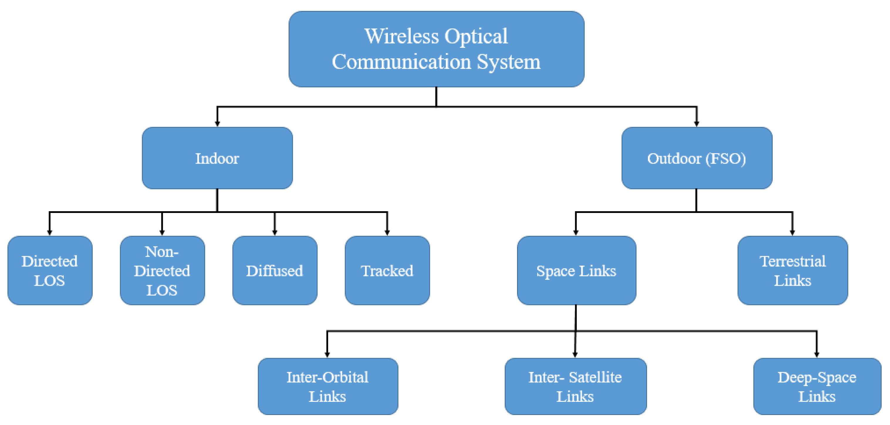
To begin with, optical wireless communications have set up different platforms and territories for placing successful communication spots. Data from Ref. [
5] emboldens the classifications of optical wireless technologies, as shown in
Figure 1.
For outdoor FSO links applications, there are two types of networks: space links and terrestrial links. The primary motivation for establishing such a network is to provide global internet coverage, i.e., the ability to communicate between any two points on Earth, particularly in areas where terrestrial internet is scarce or nonexistent. One of the pioneering technologies in satellite communications is StarLink which is described as a huge low earth orbit (LEO) constellation created by SpaceX for providing global coverage, high bandwidth, and low latency satellites [
6,
7].
For smart building communications, a line of sight (LOS) FSO link between buildings is the item of recognition and the main focus of this research. In recent years, there has been an extremely competitive aspect between conventional wireless communication such as radio frequency (RF) and the newly intriguing alternative technologies involving utilizing signals in an optical form [
8]. Among the candidate innovations these technologies offer is the FSO communication system, where a signal is transferred from an electrical to an optical one and carried through a free space medium in the form of a visible light (VL) beam or an infrared (IR) beam. The fact that FSO eliminates most of the cons of RF communication makes it a strong opponent technique nowadays [
4,
5].
The presence of linked sensors or devices in the city is required for these applications, giving the green light for new alternative linkages to step in. Mobile and network operators must adjust their strategies in this scenario to keep up with the city’s technological advancements and the conquering of other strategies and infrastructures [
9]. FSO technology displays various advantages such as non-necessity of a licensed bandwidth, high security of data and negligibility of interference and jamming occurrence, higher data rates, and cheaper rollout cost. With these advantages come some challenging situations an FSO network can encounter, including weather turnovers such as rain and foggy space, atmospheric turbulence, scintillation, scattering, etc. [
10].
Table 1 shows a detailed comparison between RF conventional wireless technology and optical wireless communications with a distinction of the bandwidth variety between RF bands and OWC bands.
FSO systems have a vast range of applications, such as outdoor wireless networks, LAN segmental small networks, optical fiber connections backup networks, backhauling, and military communications [
13]. Unlike fiber-optical installations that despite being one of the most reliable networks have the most expensive cost, FSO is a much simpler network that requires only two optical transceivers for a full-duplex link, with the proper choice of optical source used to transmit the signal [
14].
With the optimum kind of modulation depending on data rate needs and the type of territory the system is installed in, a fully-functioning low-cost communication spot is obtained [
9,
10,
15,
16]. Apart from the competitive side, RF communications happen to require complementary FSO transceiver links that can reinforce the quality of service for remotely located users and increase the overall network capacity. Another example of outdoor FSO links is presented in [
17]. To eliminate the direct LOS drawback of alignment and setup angle immobility problems multi-FSO transceivers can be tiled up to ensure the maximum spatial expansion and optimized performance for outdoor FSO links.
Designing a high-rate and resource-efficient network infrastructure for 5G and beyond has received a lot of interest and turned into an extremely viral research topic. Another hybrid example is represented in [
18], where Coexisting RF networks are integrated with optical-fiber networks and OWC systems to create an ultra-high coverage possibility for macro capacities that can handle the exponentially rising number of devices in the fifth generation evolution and IoT era. Neural networks and deep learning techniques were adaptively applied to rapidly detect the fault locations and optimize the performance of these hybrid networks.
When it comes to prototyping methodically reciprocating systems and state-of-the-art alternatives, this is where system-on-chip (SOC) technology takes place. The vast need for executing multiple and highly diverting instructions calls for hugely integrated platforms specialized in various processing techniques and distinct architectures, including microcontrollers, digital signal processors, and reliable GPUs [
19]. In recent years, the FPGA development pace has come up with a lot of chip families designers can pick from depending on the specifications required for the purposed application [
19].
The key parameter of choosing the right processing aider is the milestone of the desired application. Compatibility of the processor used with the design specifications and future modification is crucial for picking the right tool. It is difficult to find the right hardware accelerator for a given application. There are many different types of digital signal processors (DSPs), FPGAs, and graphical processing units (GPUs), and the technical distinctions between them make it hard to compare them. Although they have different built-in architectures and software interfaces, they are capable of providing design platforms. The trade-offs between one type and another are the metric of comparison.
Table 2 shows the pros and cons of using different processors.
For algorithms with high computing needs on a portable PC-independent device, FPGAs are the ideal alternative. For IBs to effectively communicate, a standalone established system that has a portable nature and dynamic capability is the optimal feature a smart network should have. FPGAs are low-power devices that may be employed in embedded systems. Instead of having separate circuitry designs that can merely cause noise and delay accumulations, resulting in falsified outputs, FPGAs help assemble the whole system in one stage [
4,
5]. Unlike other signal processing kits, FPGAs have high versatility in dealing with complex data types such as video streams, giving them the advantage of being a more reliable system hosting platform, enabling renovation and upgrading of the design to fit the most recent optimization requirements.
Different kinds of modulation are used according to the targeted data rate and the application hosting the system. There are a variety of techniques for modulating the source data into the EM wave carrier at any frequency range, including higher-level Intensity Modulation (IM) and On-Off Keying (OOK).
In [
21], an indoor FPGA-based FSO communication system was developed using an 808 nm Infra-Red (IR) 100 mW laser source in which a Zedboard comprising the Xilinx XC7Z020-1CLG484C Zynq-7000 All Programmable System on Chip (AP SoC) associated with dual cortex ARM A9 processors. A data rate of 115 kbps was accomplished at a distance of 12 m via On-Off Keying (OOK) modulation to transmit text and audio files.
In this paper, an FPGA-based FSO system is used to transfer data at a distance of 12 m at a data rate of 115 kbps via basic OOK and an optimum bit rate of 230 kbps using IM/PWM is represented using an ALTERA Cyclone IV DE2115 Board with a pre-installed RISC-V software processor and a 650 nm Visible Light (VL) 5 mW laser source. The paper is divided into four further sections.
Section 2 illustrates the idea of the implemented system.
Section 3 clarifies the implementation steps that have been carried out on both software and hardware scales.
Section 4 discusses the results obtained and, finally, the conclusion in
Section 5 summarizes the work done.
2. Materials and Methods
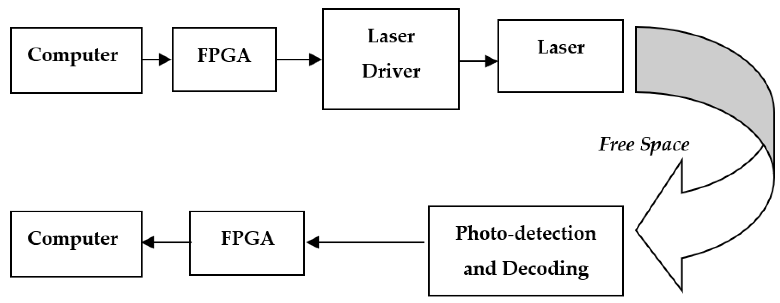
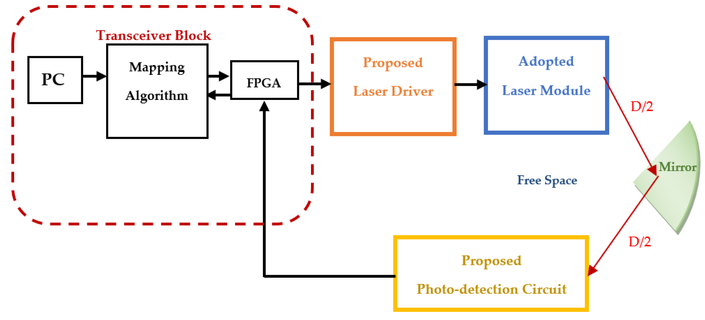
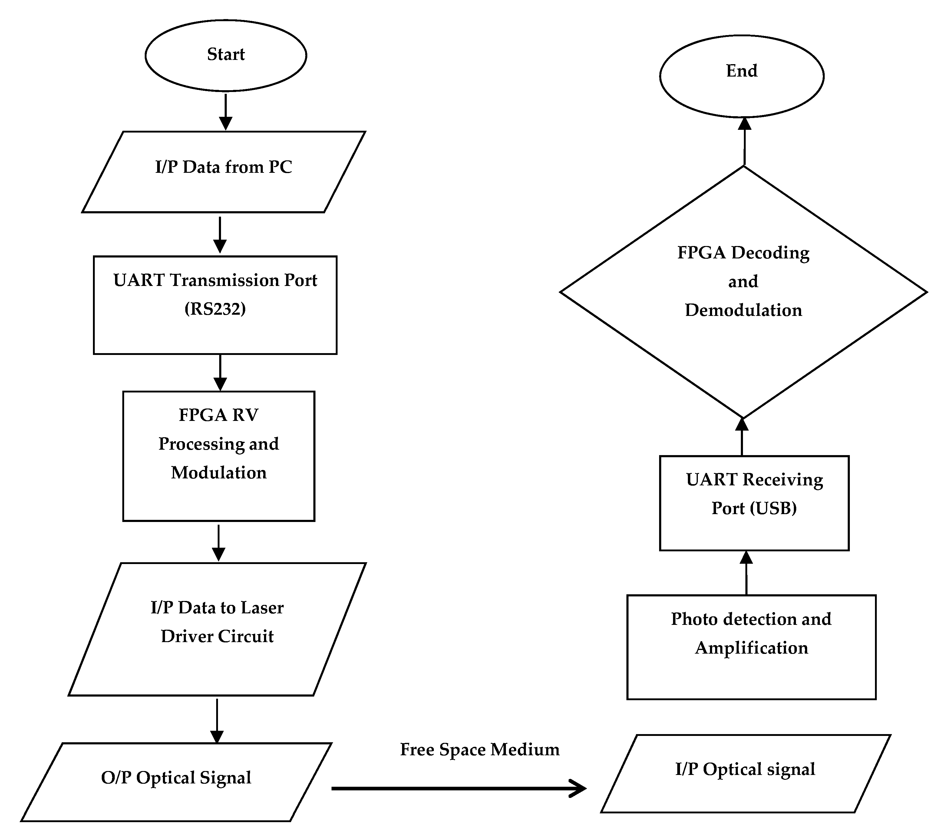
The proposed system has the computer placed as the data server. The FPGA is directly linked with each computer via a universal asynchronous receiver transmitter (UART). This interface implies the usage of a serial communication technique in which the data is sent into the FPGA for processing and modulation. Reduced Instruction Set Computer Five (RISC-V) is installed into the FPGA for managing the sent data. The modulated data is streamed from the FPGA, as shown in
Figure 2, to the laser driver circuit at the transmitting terminal, where the signal is amplified and converted from an electrical signal to an optical one. The red laser source was selected as the transmitting module due to its low cost, adaptability, and high data rates endurance. Focally concentrated beams that can travel long distances are also one of its landmarks, thus it is a gradable versatile light source. The channel is conceptually a free space line of sight (LOS) medium.
Modulation schemes are one of the key factors that affect the performance of a communication system, given that the major drawback an FSO link can suffer from is a bad weather channel condition. Attenuation jeopardizing the quality of the received signal is the main driver of the transmitter specifications, including transmission configuration and the modulation scheme used. Originally, OOK is the simplest form a signal is modulated by where only one bit is sent in each clock cycle, where digital 1 is represented by full illumination, while digital 0 is represented when the laser is off [
22]. The OOK is frequently plagued by spectral and energy efficiency issues. This sort of modulation approach also has amplitude distortion as a disadvantage. One way to overcome the drawbacks of OOK is using other modulation techniques such as Pulse Width Modulation (PWM) and Pulse Phase Modulation (PPM), where the amplitude interpretation is eliminated in the signal detection. Another “optical compatible” modulation technique that has shown a favored performance in the FSO system is IM. In IM, information is retrieved at the receiver side by detecting the intensity of received light, which is modulated as an information-carrying signal. Opposite to RF conventional communication that may include complex types of data, intensity-modulated signals are rather positive and real-valued [
23]. Besides bypassing the OOK disadvantages, its simplicity and low-cost installation are other advantages of the IM technique. Reconfigurable algorithms can be established to pick the optimum modulation technique according to the type of data, transmission distance, and channel model. In this research, the implemented system initiated a study that compares the realization of OOK and IM schemes in terms of data rate since these two modulation schemes are the most commonly used in FSO implementations, and the fact that IM can be integrated with other modulation techniques that control the light intensity makes it an interesting approach for further optimization and modification. Higher-level IM, on the contrary, uses a single clock cycle to transmit more than one bit depending on the number of levels that power would be divided into. The power ratio then encodes the bit symbol into a certain voltage level that controls the illumination of the laser beam. Here, this is done by controlling the pulse width of the output transmitting power.
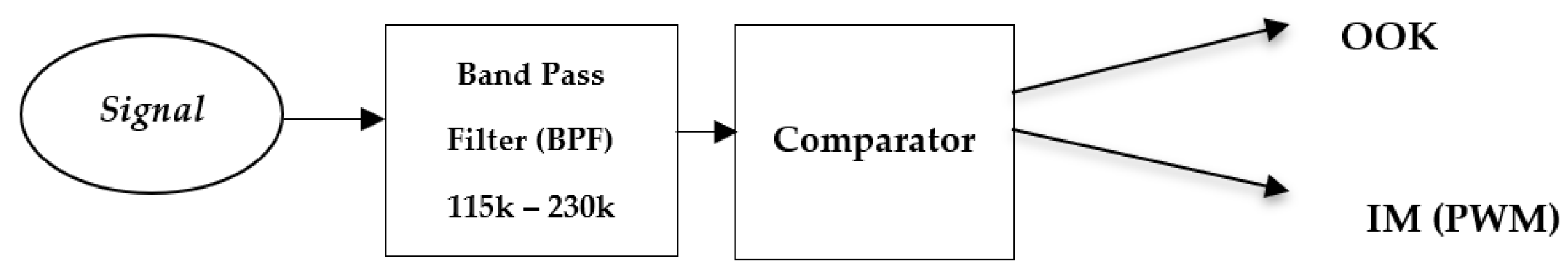
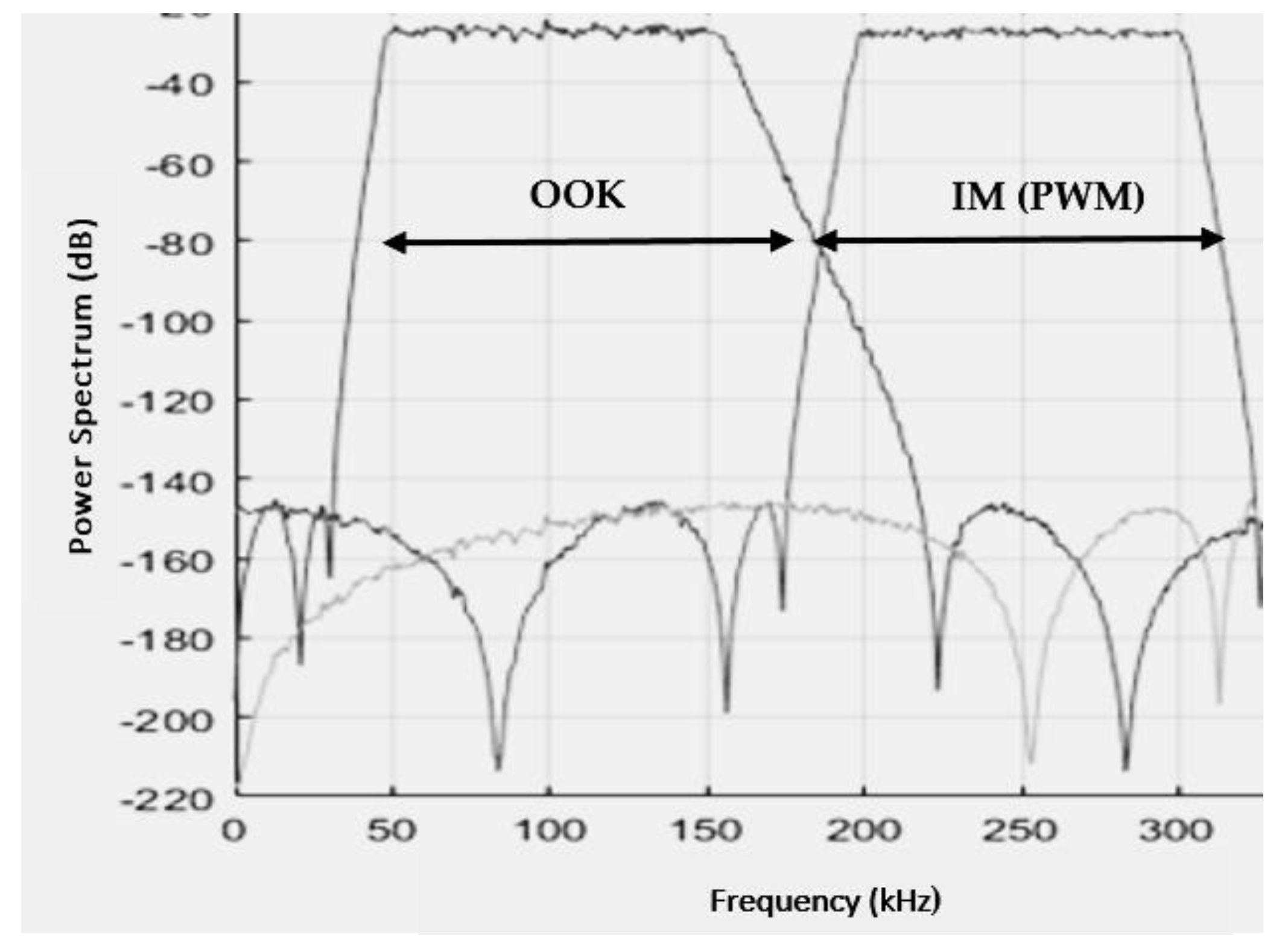
A mapping algorithm is completed using MATLAB to compare the frequencies of the incoming data. As shown in
Figure 3, if the frequency happens to be less than or equal to 115 kHz, OOK is used. Otherwise, IM is the chosen technique. Thus, the most suitable modulation is configured for reliable communication with less power consumption.
Figure 4 shows how bandpass filters (BPF) can filter out random data ranges to determine the desired modulation used. These BPFs can be adjusted according to any further desired data frequency ranges. The FPGA was the kit of target due to being a compatible environment in which hardware building and reconfiguration is a fast process with easy modification availability. It also enables designers to create a bottom-up implementation of any hardware system prototype, ensuring that the final product is bug-free.
Channel Model
The received signal model in wireless communication systems is generally represented in (1).
In which
x(t) is the original signal;
h(t) is the channel effect function;
and n(t) is the summed-up noise.
The total received signal is the resulting combination between the original signal x(t) convoluted with the channel effect function h(t) and additional noise n(t) summed up in the transmission. That noise is mostly implicating light surroundings, thermal noise, shot noise, and dark currents that are modeled as Additive White Gaussian Noise (AWGN). The encountering interferences and jamming threats upon RF signals are eliminated due to the high immunity of optical signals.
One of the key installation parameters FSO links are prone to consider is the angle of transmission. For rooftop applications requiring LOS frequent availability, the light beam emission angle must be aligned with the receiver position at a horizontal (180°) angle with a slight acceptable error of ±5° about the photo-detector area collecting the optical signal [
24]. This gives total power (in watts) emitted from a uniform source, as represented in (2).
In which
is the total transmission power;
B is the brightness function;
is the surface area;
and is the emission angle.
The above equations are valid for any free space communication link performance analysis. With the aid of a converging lens, the light from the source beam can be concentrated on a single point to reduce attenuation levels and scattering losses. For the used laser source, a focal lens is adopted to focus the output optical signal. The source has an aperture of 12 mm in a dot shape. The module is set perpendicular to the mirror interface at 90° so that the silicon-based photo-detector of 7.5 mm2 and sensitivity angle φ = ±65°. For fixed transmission angle, sensitivity angle, and receiving surface area, the brightness becomes a function of the total transmission power.
3. Implementation
This section is divided into two parts: software and hardware. The software part of the system is encapsulated in the processing done on the ALTERA FPGA Cyclone IV DE2-115 board that has a RISC-V processor software version installed for input data management. RISC-V is an open specification platform that allows designers to use open-source cores, utilized at low power mode, unlike ARM, Intel, and AMD processors, which need licensed products, owned IP, and use complex instruction set computer (CISC) technique, hence, they have high power consumption. Newly intriguing computing methodologies and integrating engineering applications acquire the presence of robust simulation and testing kits that can stimulate the process of innovation in both software and model-ware forms, which are capable of supporting and validating the design flow. Model-ware, often known as Model-Driven Development (MDD), is a broad area that supports a variety of technologies by increasing software development productivity. With highly defined software isolation domains that are continuously up to date, developers can frequently upgrade their designs and ensure the security of data [
25]. It is highly used for multimedia applications and file compressions, thus an optimum processing option for the proposed design.
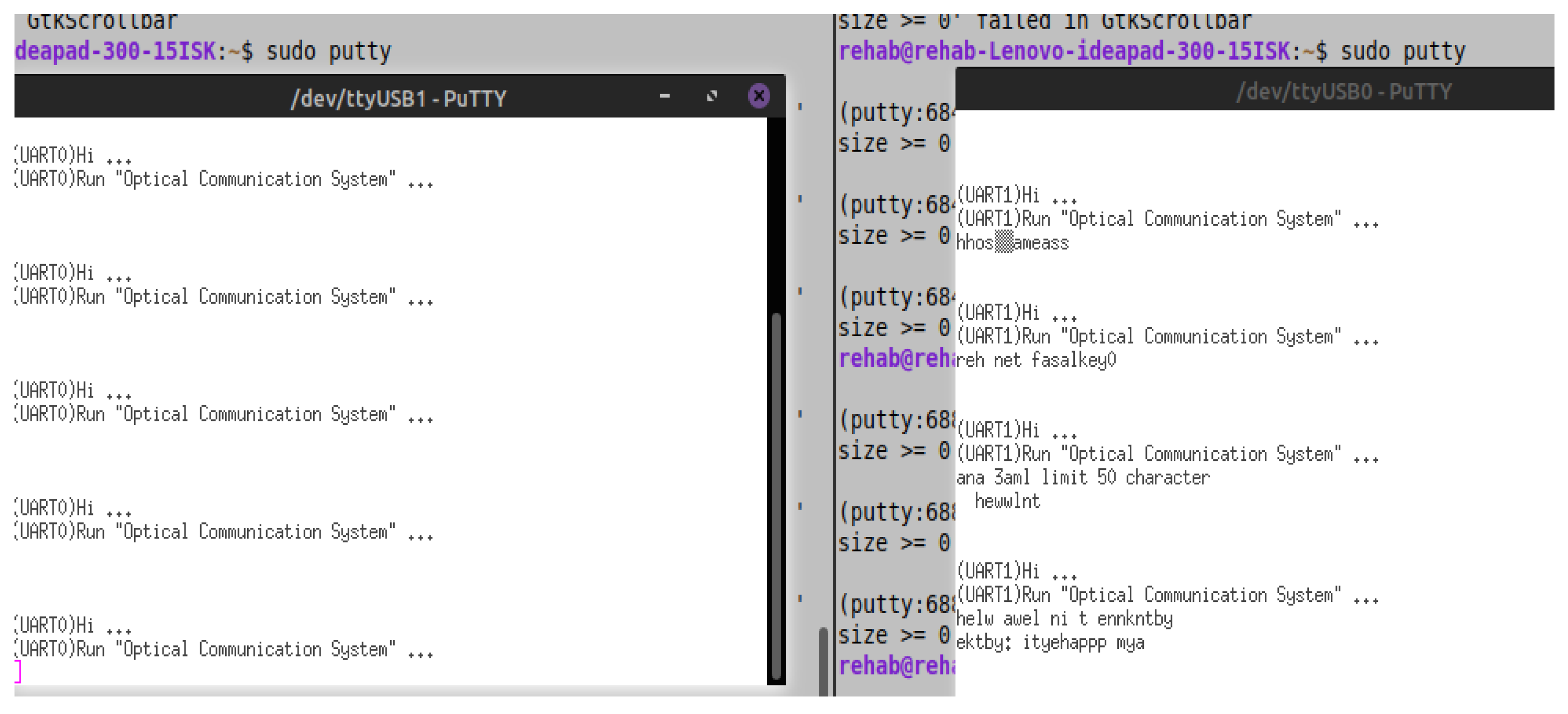
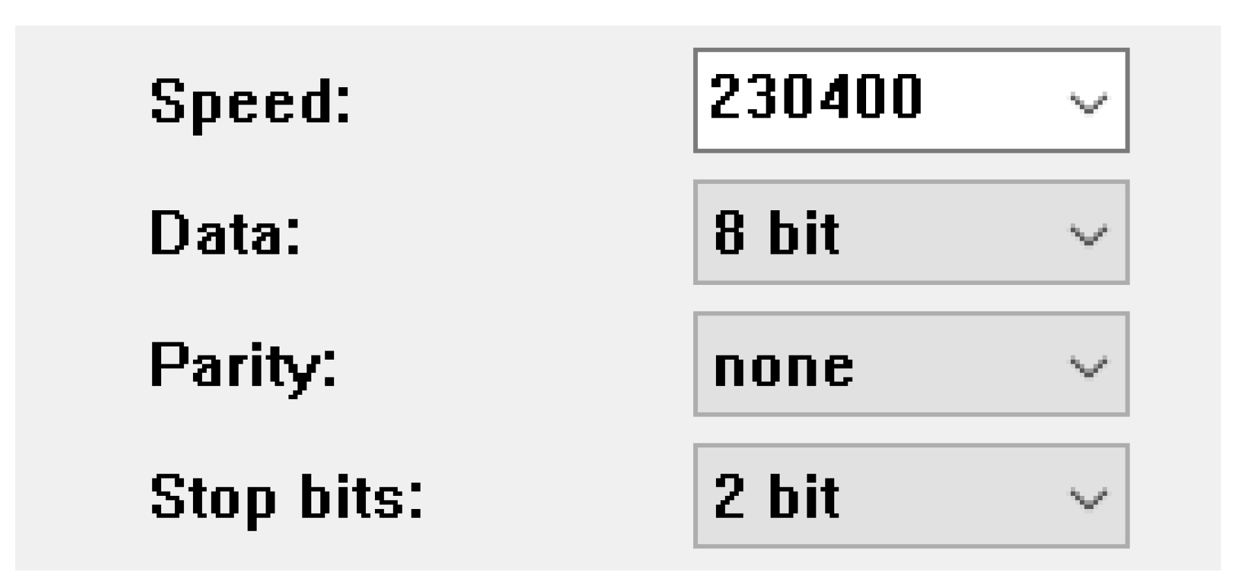
The communication between the FPGA and the computer is obtained via a Universal Asynchronous Receiver Transmitter (UART) RS232 cable for transmission and a Universal Serial Bus (USB) for the reception. The proper modulation technique is selected according to the required data rate and mapped to be performed by the software interface (Quartus Prime 18.0) of the FPGA. Higher-level Intensity Modulation (IM) was the item of choice, controlling the illumination of the laser beam accordingly. Four power levels were given as the constellations of data required to be transmitted. The levels were represented as 0%, 33%, 66%, and 100% of the power. Tera Term and Putty user interfaces were used to test the data sent in a text form, while MATLAB was the test bench used for audio data.
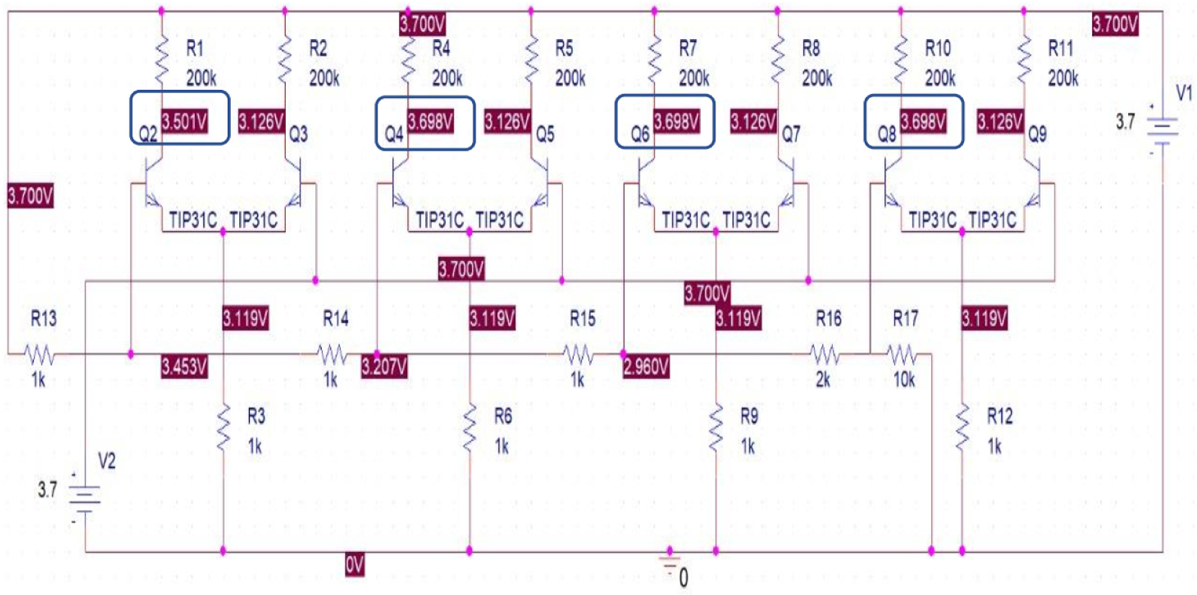
The modulated signal is fed from the FPGA General Purpose Input Output (GPIO) into a laser driver circuit where it is amplified using a common emitter configuration amplifier manifesting the selection of a TIP31C power transistor that boosts the transmission into a 650 nm Visible Light (VL) red laser source. The FPGA input signal is directed to the base of the transistor while the output signal is taken from the collector to the laser source, as shown in
Figure 5. The emitter is connected to a 3.3 V supply.
If the o/p of a collection of circuits linked as a system reaches a fixed value in a finite time, it is said to be stable. A system is considered to be unstable if its o/p rises with time rather than stabilizing. Multiple ways are used to determine the stability of a circuit. For BJT stability, the rate of change of collector current with respect to the reverse saturation current can be the metric of stability measurement. The maximum collector-base voltage in saturation mode is 1.2 V at a collector current I
C = 3 A, while the transit frequency for current gain is f
T = 3 MHz at I
C = 500 mA [
26]. The operating margin for the BJT is ensured, and a consistent current flows via R1 and is supplied into the laser module since the circuit is run in low power mode, with V1 continually 3.3 V plugged out of the DC port on the FPGA board and Vin dependent on the set character voltages from the PC. Hence, the input current to the laser module is constantly stabilized in the range of milli Ampere.
The optimal transistor was chosen based on the power amplifying specifications required to transfer the optical signal at the greatest possible distance. After experimentations, the application of the TIP31C transistor became apparent. When considering power amplification abilities and the fact that the optical signal required a highly powered-up gain to traverse the requisite distance between the transmitter and the receiver, there was a significant performance enhancement.
A mirror reflects the laser beam at half the distance (D/2) back to the photo-detector to achieve a distance D of 12 m between the transmitter and the receiver. The existence of the mirror was used to verify the system’s compatibility in outdoor settings between adherent buildings or in the design of multipath signals employing smart building mirror glazed architecture. Double the setup distance is achieved by practically inducing the mirror to reflect the signal at half the distance D/2.
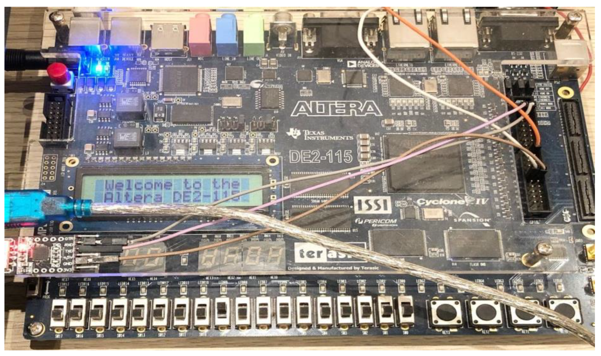
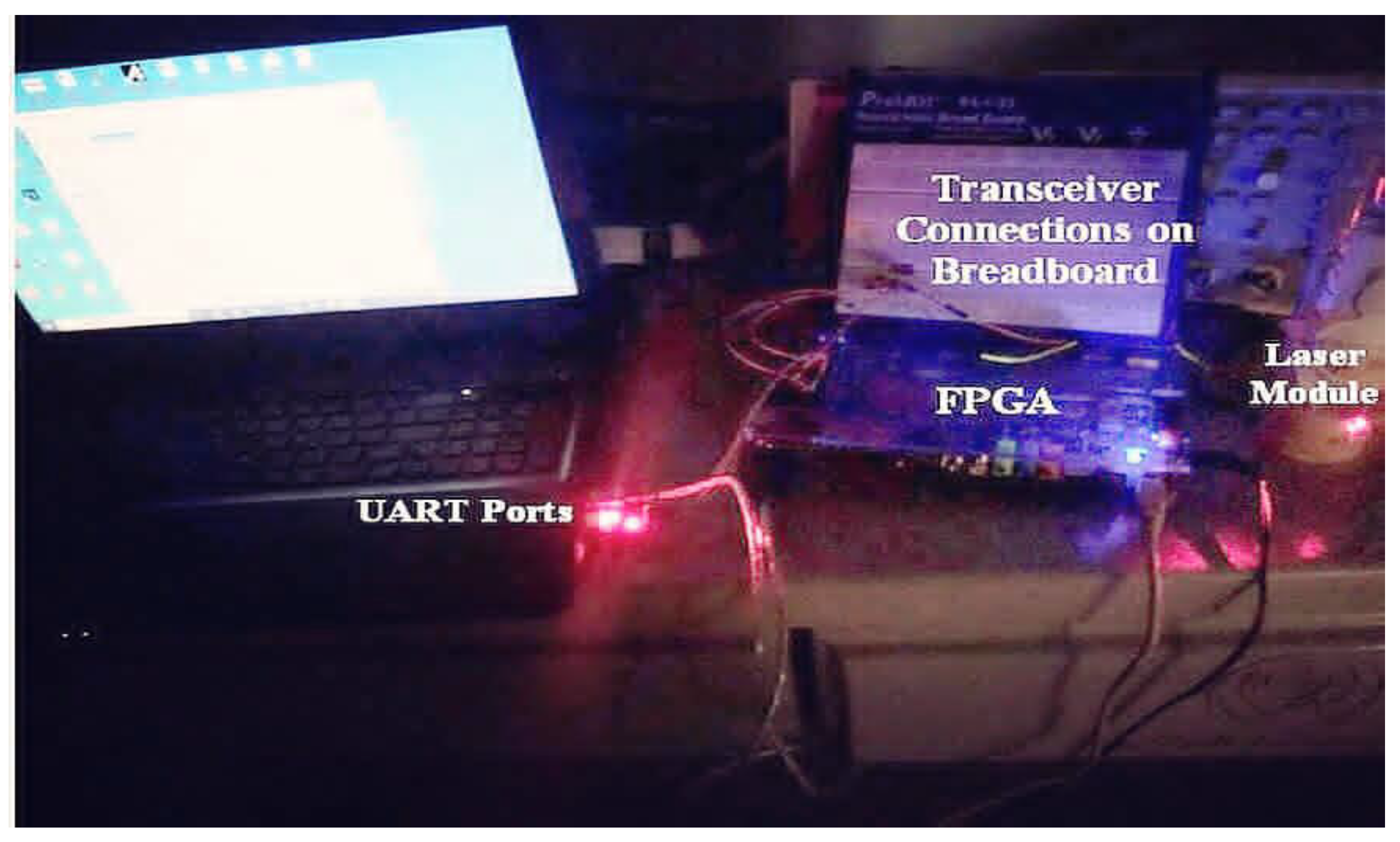
Figure 6 shows the practical system setup for complete hardware testing. The use of building walls as transmission points between one another with the concept of numerous signal reflections is emphasized by the fact that smart buildings present the idea of glazed exterior layers. Hence, adapting multi-node FSO networks can be installed.
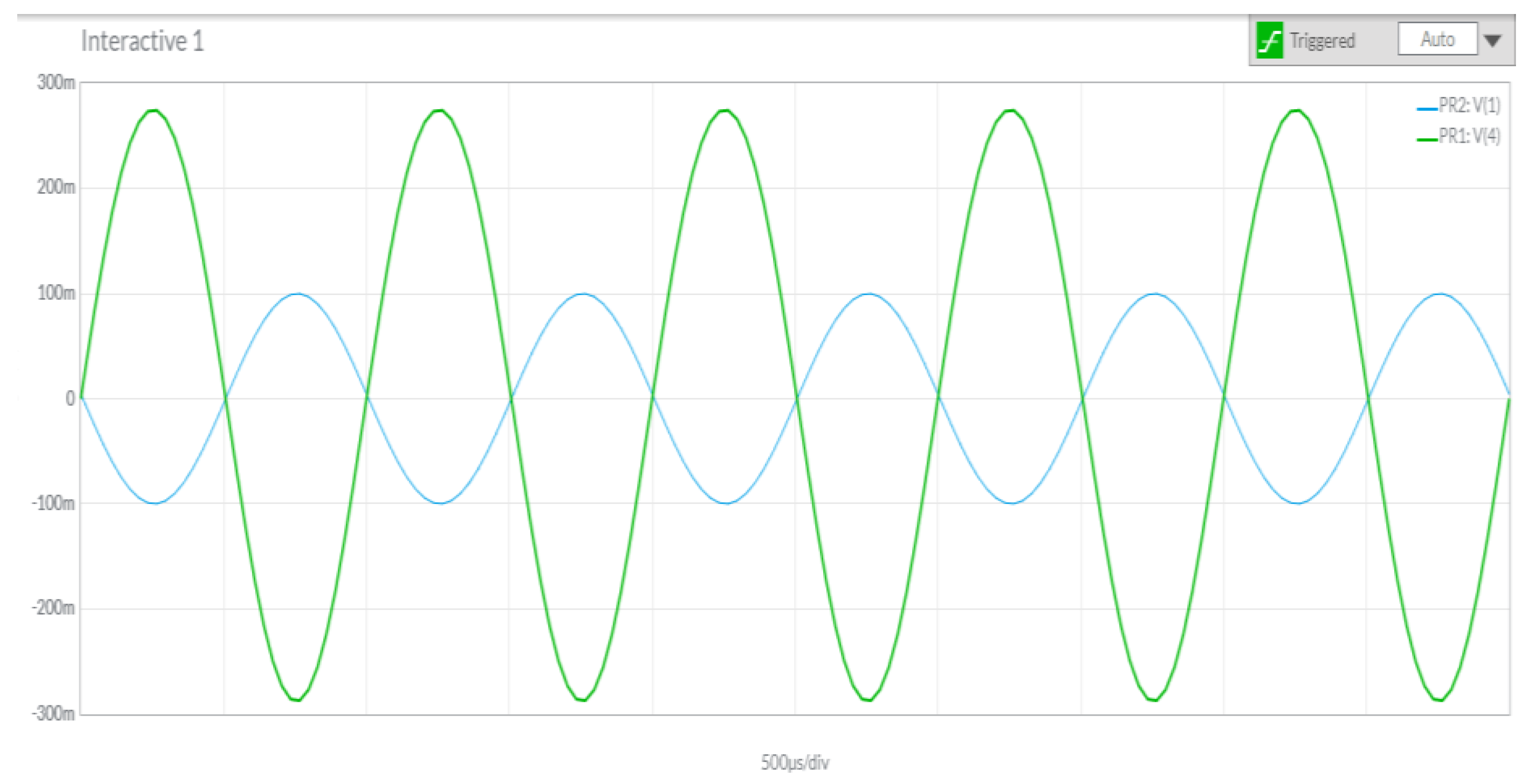
Figure 7 shows the schematic and amplification of a 100 mV input signal via a common emitter amplifier circuit using TIP31C. The output voltage has shown an increase to around 270 mV amplitude with the use of the TIP31C transistor, as shown in
Figure 8.
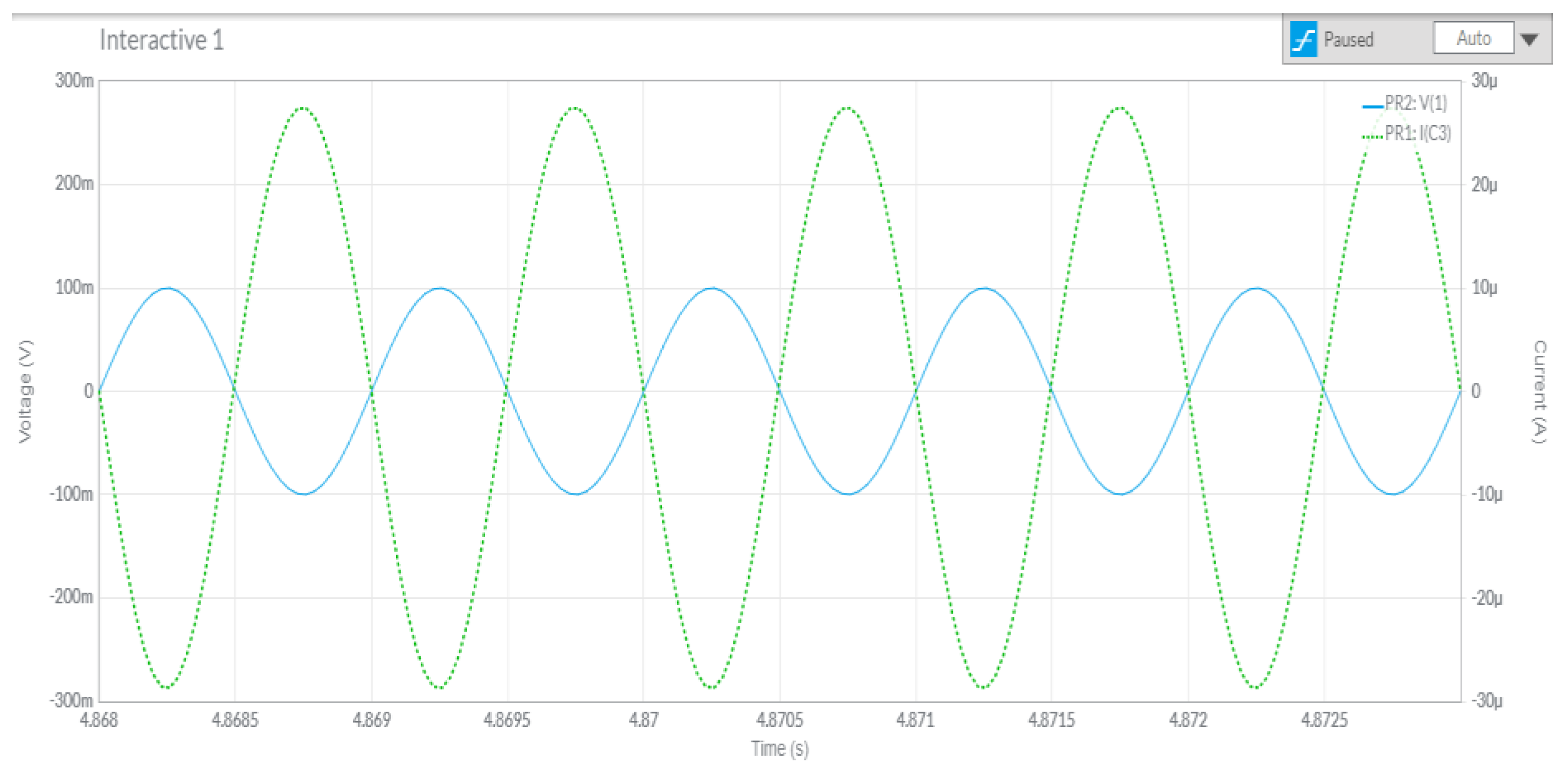
Figure 9 also shows the o/p collector current against time for the given sample circuit. This has demonstrated the dependability of using the TIP31C transistor as the driver and photo-detection circuit’s building block. It was also demonstrated in the hardware deployment that the increase in gain allowed the optical signal to be more illuminated and travel the required distance.
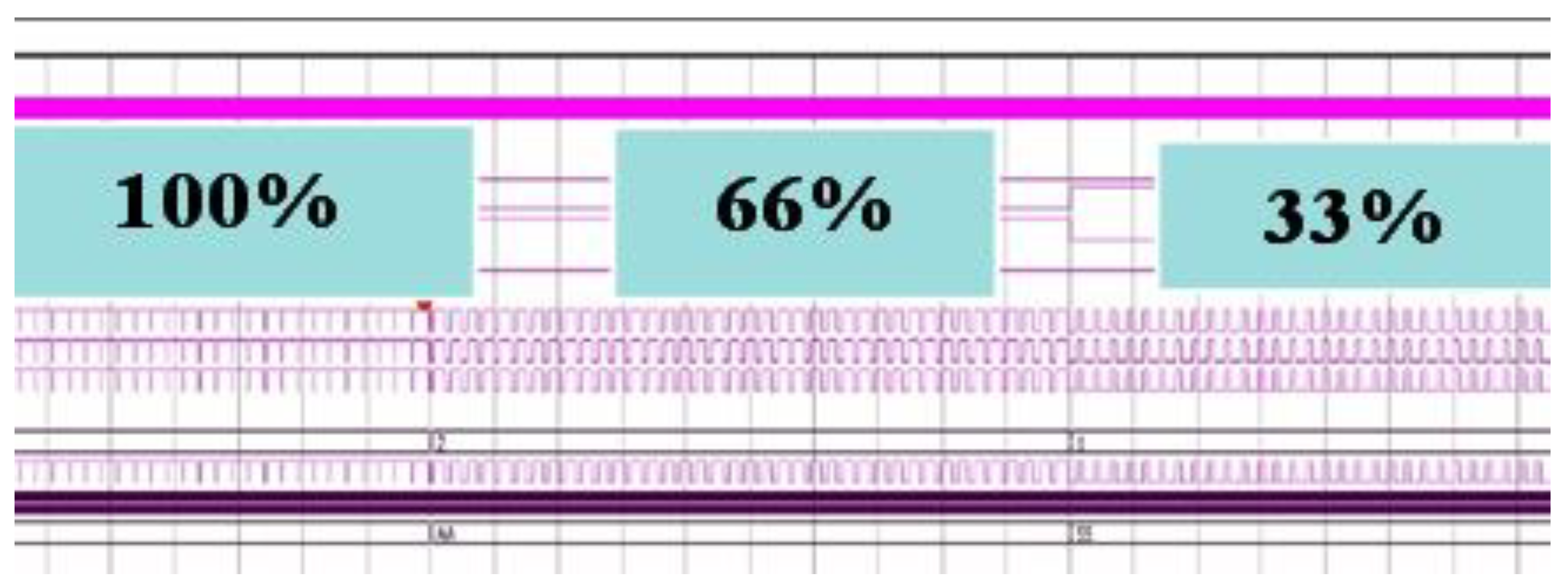
The power levels were properly adjusted to meet the targeted four laser intensities in the VHDL part, as shown in
Table 3, using a trial testing of the amplitude of the voltage for optimum detection of the received bits. The levels are initialized in a hexadecimal form.
Figure 10 shows the simulation results on ModelSim. The pulse width of the waveform represents the percentage of power for each illumination level.
The laser light intensity varies along with the distinction of the data being transmitted, and the beam is carried in free space from the transmitting to the receiving point. At the receiver terminal, the BPW34 Photodetector catches the optical signal where it is reverted to an electrical one. BPW34 is a silicon-based high sensitivity photodiode packaged in a plastic capsule with a water-clear epoxy surface texture. It can detect visible and infrared radiations. Its detecting area is considered relatively high (A = 7.5 mm
2) with a wide varying viewing angle (φ
s = ±65°). The reverted electrical signal is then passed to a comparative Analog to Digital Conversion (ADC) demodulating circuit, as shown in
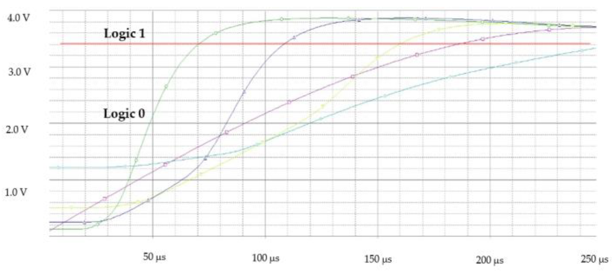
Figure 11, to interpret the four voltage levels into logical ones to be read by the receiver USB port from the FPGA into the computer via the GPIO input pin. The circuit is constructed using the concept of the differential pairing of TIP31C BJT. Here, a combination of four comparative differential pairs is used to measure the difference between the reference voltage and input laser voltage for a maximum value of 3.7 V. If the input voltage is greater than the reference voltage, the output voltage will be 3.7 V (Logic “1”), as shown in
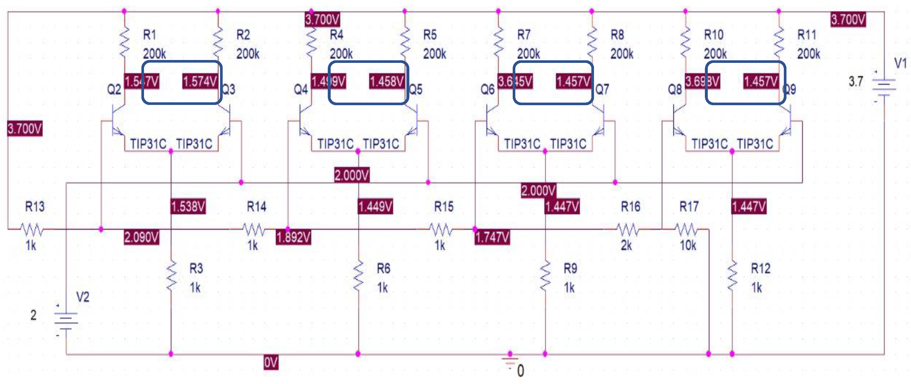
Figure 12. There are four reference voltages for each comparator so the output will be divided into four logical levels according to the input analog voltage.
The components used to build up the proposed system are listed in
Table 4.
Figure 13 shows a flowchart intensifying the algorithmic approach accomplished by the system, stating logically how data flows from the transmitting to the receiving point.


