1. Introduction
Trapping techniques use engineered forces to accurately control and manipulate objects in mesoscopic systems with length scales from tens of nanometers to hundreds of micrometers [
1,
2]. The understanding of the light interaction with the matter at a micro/nanometer scale paves the way to improve the knowledge of the properties of materials and the use of trapping in interesting application fields, such as sensing [
3] and quantum systems [
4]. In particular, the main capabilities of the trapping techniques have been exploited in the natural sciences fields, primarily in support of modern medicine, i.e., for monitoring inter- and intracellular processes or the manipulation of viruses and bacteria [
5].
Since Ashkin’s pioneering research [
6,
7], optical trapping configurations have been developed to trap small cells and bacteria [
8], first preventing the contact of the target with the device and then damaging or disrupting the target object, as required in non-invasive medicine. Conventional optical trapping techniques exploit the forces exerted on the target by focused laser beams [
9]. However, although bulk tweezers with focal lenses that provide an effective trapping of micro-sized particles are largely used, this approach suffers from low optical gradient force, due to the diffraction limit, and trapping situ larger than the particle itself. To overcome these challenges, the development of efficient trapping devices remains a hot research topic [
10].
An optical approach ensures a high trapping efficiency and the stability of the target object in the trapping situ. During recent decades, several configurations of photonic devices, mainly based on photonic resonant devices [
8] such as photonic crystals [
11,
12] and ring resonators [
13,
14], plasmonic devices [
15], or hybrid configurations [
16,
17], have been demonstrated. Photonic resonant devices have been proposed as optical tweezers, to exploit their high spectral and spatial energy confinement, which strongly depends on the high
Q-factors and low mode volume. The trapping of a single protein using a power of 10 mW has been experimentally demonstrated in [
18] by using a 1D PhC cavity, with a stiffness
k in the order of hundredths of fN/(µm/mW). Nevertheless, a stable trapping of polystyrene particles with diameters of 500 nm and 200 nm has been demonstrated with a silicon-based ring resonator [
13] and microdonuts [
19], respectively, with optical power in the order of microwatts. The short trapping time represents the main bottleneck of photonic resonant optical tweezers, mainly caused by the optical gradient force not being sufficient to trap the target for a “long” time. To mitigate this issue, engineered photonic resonant configurations, as metasurfaces, have also been proposed in the literature, to ensure an efficient trap of thousands of objects, with a power value density less than tens µW/site and optical forces of tens of fN, at the expense of a larger footprint and higher complexity [
20]. To overcome such issues, plasmonic antenna systems have been proposed, aiming to control light at the nanometer scale with a large electromagnetic field within deep subwavelengths volumes [
15]. The plasmonic enhancement is strictly correlated with the near- and far-field properties of metallic nanostructures that confine the light within small volumes and amplify the intensity of optical fields by orders of magnitude, so that they are useful in surface-plasmon-sensing applications [
21]. The trapping of particles with diameters of tens of nm has been experimentally demonstrated by using different plasmonic configuration, such as coaxial apertures [
22], single/double nanoholes [
23,
24], and bowties [
25], with very low optical power values (≈mW) and stiffness of hundreds of fN/(nm/mW). However, the critical challenge of the plasmonic trapping configurations is related to the thermal effect, due to the Joule effect caused by the strong absorption loss of the metal layers at high operating frequencies, which could lead to thermophoresis or the boiling of the fluid surrounding the particles [
26]. These effects could irreversibly undermine the biological sample and then affect the robustness of the measurements. Countermeasures have been proposed to mitigate similar behavior, such as integrating a high thermal conductive heat sink with the plasmonic nanoantenna [
27] or exploiting the heat sink behavior of the metallic film itself [
28]. However, even when using these techniques, the temperature surrounding the sample is still high (in the order of a few
K). This challenge led to the development of dielectric nanoantennas, preventing the thermal effects with simple configurations and high stiffness [
29,
30,
31,
32]. The high electric field confinement of dielectric antennas is ensured by their strong electric and magnetic resonant modes, known as “hotspots”. Worsening temperatures, correlated with strong electric field confinement, are prevented by using high thermal conductive materials such as silicon. In this context, the efficient optical trapping of 20 nm and 100 nm polystyrene nanosphere has been demonstrated by using two silicon pillars within a ring resonator, with a stiffness of about 0.01 fN/(nm/mW) and an optical power of about 10 mW [
29]. Recently, dielectric bowtie nanocavities have been also theoretically investigated [
30,
31], demonstrating a deep subwavelength mode volume and high Q-factor, with a relatively high Purcell factor. Although these devices have been proposed for several applications, such as a high-efficiency single photon source, threshold-less nanolasers, and cavity QED strong coupling experiments, the capability of this device as an optical tweezer has not yet been proved, to our knowledge [
30,
31].
Here, we propose the investigation of a nanocavity made by silicon tip-to-tip triangles acting as optical tweezers for trapping beads with a diameter of 100 nm, as the common
Coronaviridae or
Paramyxoviridae virus family. The energy field confinement within the trapping site has been maximized by engineering the wedges and then tailoring the “slot” and “antislot” effect, as described in the next few sections. The improvement of the energy confinement within the trapping volume preserves the efficiency of the trapping with regard to any manufacturing/setup issues, making the proposed device robust with repeatable performances. A force along the normal axis of 27.45 fN, with stiffness of about 0.33 fN/nm, has been calculated for the trapping of a 100 nm bead with an input power of 5.77 mW and a temperature change of 0.3 K that correspond to a trapping stability S = 1, ensuring a stable trapping for several seconds, as stated in [
29]. All these features, combined with the robustness of fabrication, make the proposed device suitable for multifunctional applications based on light–matter interactions, including enhanced spectroscopy, SERS, fluorescence, and biosensing.
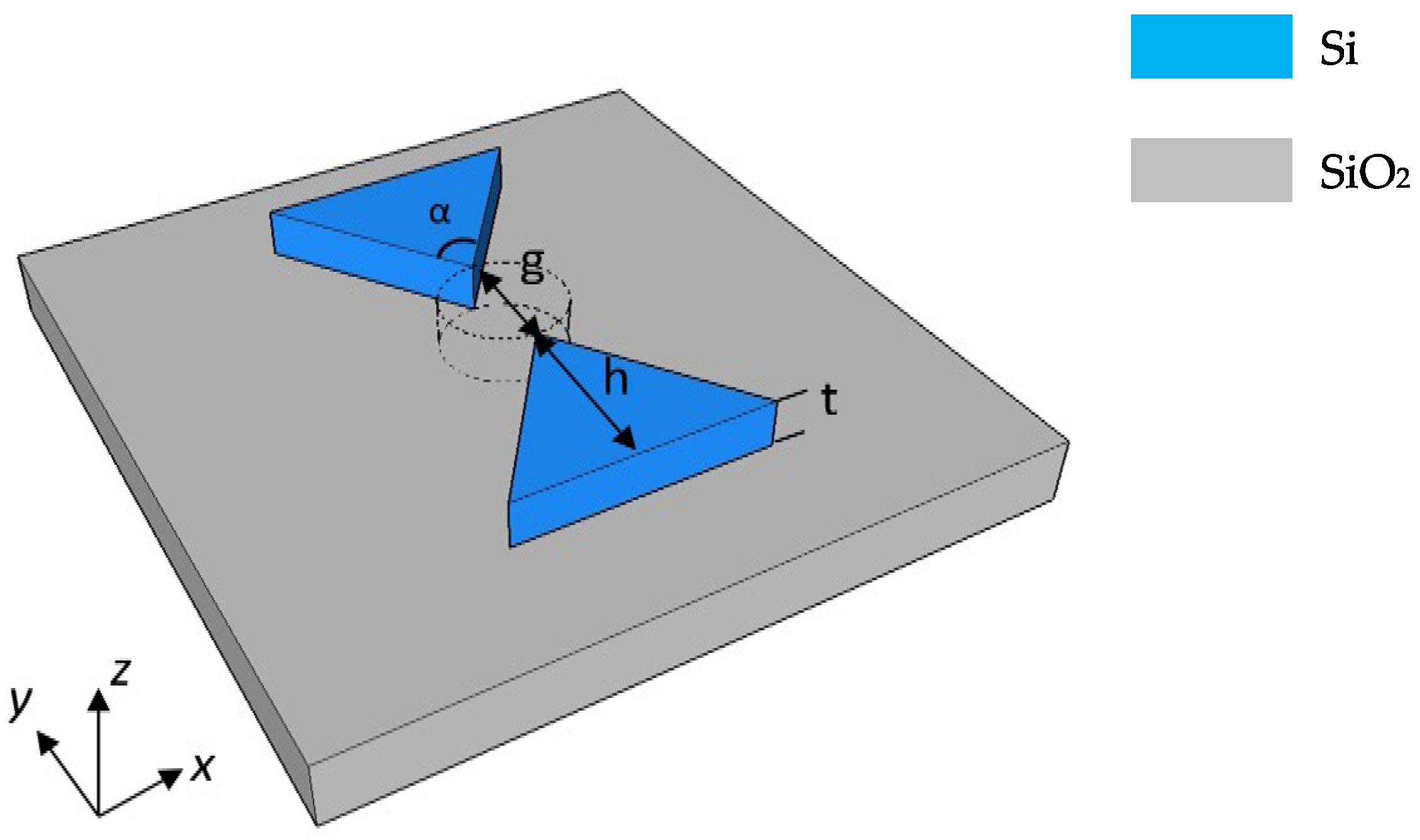
2. Dielectric Bowtie
The proposed device consists of a three-dimensional dielectric nanocavity, including two tip-to-tip semiconductor wedges (
TTSWs), forming the so-called nanobowtie dimer shown in
Figure 1, realized in Silicon-On-Insulator (
SOI) technology. The
TTSWs have the same physical and geometrical features, with an out-of-plane light excitation along the z-axis. In particular, the silicon-based dimers show a thickness
t equal to 220 nm, placed on top of a silica dioxide (SiO
2) layer. The
TTSWs show a wedge shape, with a height
h and a wedge tip angle
α.
The wedges are symmetrically placed with respect to the center of the trapping site, sketched with a dotted cylinder with a diameter equal to
g, and spatially separated by
g. The proposed configuration is surrounded by water (H
2O), used to transport biological species. Although small wavelengths are preferred in order to enhance the trapping efficiency by reducing the scattering force [
33], this benefit is mitigated by a gradient force proportional to the operating wavelength and by a strong field confinement within the trapping region, in nanoscale, in a large spectrum region. Moreover, the low cost and easy availability of the light sources at telecommunication wavelengths paves the way to their use in several applications, including optical trapping [
34]. Therefore, an operating wavelength
λ0 equal to 1550 nm is assumed, as in [
34]. The relative refractive indexes of Si, SiO
2, and water, at 1550 nm, are
nSi = 3.48,
nSiO2 = 1.444, and
nH2O = 1.318 + 9.86 × 10
−5 i, respectively [
35,
36,
37].
The electromagnetic behavior of the proposed configuration results from the exploitation of the first Boundary Condition (BC), which requires the continuity of the normal component of the electric field displacement. It ensures that the maximum of the electromagnetic energy density is confined to the low-permittivity region (slot effect) that is greatly increased with respect to the maximum energy density in a high-permittivity material, such as the
TTSWs. The slot effect ensures the squeezing of the mode along
y and
x axes in the dielectric gap, resulting in a large electric field discontinuity at the high-index contrast interfaces, with a consequent light enhancement and confinement, and the electric field enhancement (“hotspot”) in proximity of the wedge tip of each
TTSWs [
38,
39].
Therefore, the
TTSWs function as capacitors, with the energy stored in the low-permittivity region (dotted cylinder in
Figure 1).
3. Design to Enhance the Energy within the Trapping Site
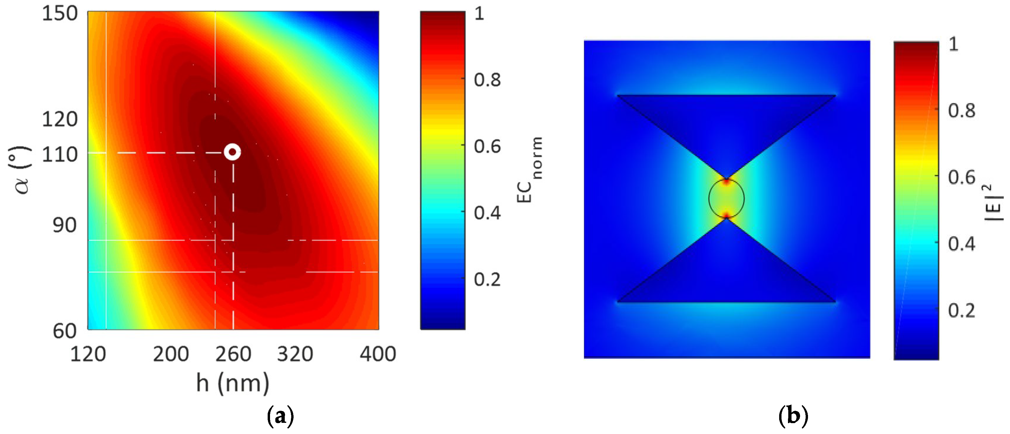
The proposed configuration is designed to maximize the electromagnetic energy confined in the trapping site. The most common approach to designing optical nanocavities aims to minimize the effective area of the mode in the trapping region [
15,
16,
30,
31], expressed as the ratio between the integral of the electromagnetic energy density and its maximum. However, this approach neglects the amount of energy confined in the trapping site, confining the mode in a small volume and then becoming very sensitive to manufacturing issues. Therefore, we have introduced a new figure of merit, EC, representing the energy confinement in the trapping site, expressed as the ratio between the integral of the electromagnetic energy density in the trapping site and the integral of the electromagnetic energy density in the whole volume surrounding the nanoantenna:
where W(r) is the electromagnetic energy density
and
. This figure of merit responds to the need of a high energy confinement within the trapping to ensure a powerful trapping even with a small mode volume.
As previously reported, the trapping site is considered a fictitious cylinder with a thickness
t and a diameter
g. Since the target molecule to be trapped shows a diameter of about 100 nm, such as the RNA-based
Coronaviridae or
Paramyxoviridae virus families [
40,
41], a gap
g of 120 nm is suggested, based on a conservative approach, to ensure the fabrication robustness by avoiding the particle sticking at the tips. A 3D Finite Element Method (
FEM) approach is used to simulate the electromagnetic behavior of the investigated configurations. In particular, the device is designed to define the best configuration in terms of
α and
h. The 3D mapping of the normalized figure-of-merit EC
norm is shown in
Figure 2a, with an impinging optical power
Pnorm = 1 mW/µm
2 polarized along the y-direction. The inconstant behavior of the electric energy confinement in the trapping site is due to the spreading of the electromagnetic energy in the in-plane cladding layers, for configurations with
h < 260 nm and
α < 110°, or in the silicon wedges, for configurations with
h > 260 nm and
α > 110°, due to the additional high-permittivity antislot effect. In the remaining regions, the electromagnetic field moves from high to low, or vice versa, in the permittivity region.
This effect is related to the fulfillment of the second boundary condition that requires the continuity condition of the tangential electric field between two different materials. Therefore, this effect spreads the electric field in the trapping site with a consequent decrease in the electric field confined in the trapping region.
The configuration with
α = 110° and
h = 260 nm shows the highest normalized EC, expressed as EC
norm, (white empty circle in
Figure 2a), as shown by
Figure 2b, with a resulting total footprint
A of about 0.96 µm
2. The major component of the electric field is along the y-direction, representative of the quasi-
TE polarized mode in the nanocavity. The electromagnetic energy density is mainly confined within the gap region, without spread in the cladding or dielectric material, typical of the slot effect, ensuring a stable trapping of the target particle.
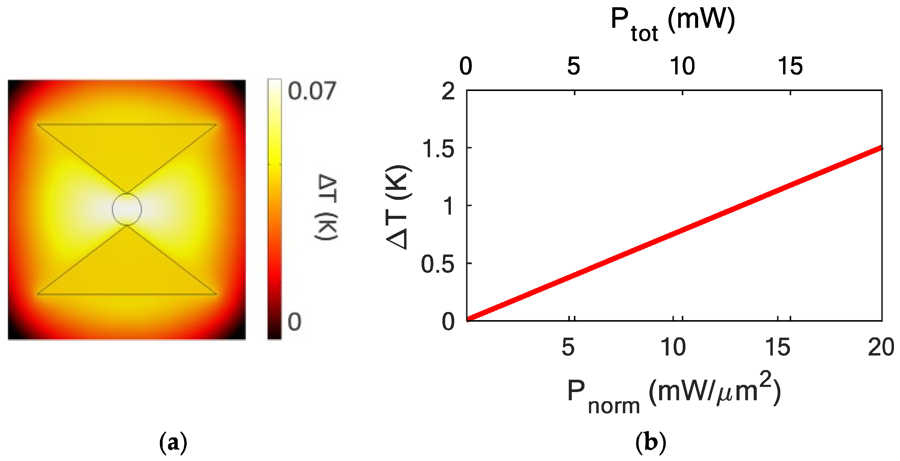
In order to demonstrate the overcoming of the heating problems related to plasmonic nanoantennas, numerical simulations on the temperature behavior were carried out. The top view of the steady-state temperature distribution for the investigated configuration is reported in
Figure 3a by considering an input optical power of 1 mW/µm
2. The temperature rises in correspondence with the trapping site, where the electromagnetic density is highly confined, as expected, with a maximum temperature increase ΔT of 0.07 K. Moreover, the ΔT change created by varying the input optical power
Pnorm, and then the total optical power
Ptot (=
Pnorm ×
A) has been calculated (see
Figure 3b), measuring a slope of 7.51 × 10
−2 K/(mW/µm
2). Similar values confirm the suitability of the dielectric nanoantennas for biological species trapping, because of the negligible temperature increase in contrast with the plasmonic nanoantennas where an increase in temperature of about 100 K has been obtained in [
29], caused by the thermophoresis effect. The small temperature growth also preserves the vitality of the trapped biological species.
4. Numerical Results on the Optical Trapping and Discussions
Three-dimensional
FEM simulations with the Maxwell Stress Tensor (
MST) approach have been used to calculate the optical forces exerted by the proposed nanocavity on a spherical particle with a diameter
d of 100 nm and a refractive index equal to 1.50, representative of some viruses, i.e.,
Influenza A [
42,
43] and
HIV-1 [
44]. The software COMSOL Multiphysics
® has been used for e.m. and thermal simulations by combining the heat transfer and optical physics. According to the method described in [
45], we have evaluated the optical force as the surface integral, on a surface with a radius few nm larger than the particle radius, of the vectorial product of the Maxwell stress tensor and the outgoing vector normal to the surface.
In particular, the optical forces have been evaluated on the particle under test in different positions along the x, y, and z axes. The positions x = 0, y = 0, and z = 0 correspond to the central point of the trapping site at the Si-SiO
2 interface (see
Figure 4). In order to estimate the trapping efficiency of the designed structures, the optical forces F
i (i = x, y, z) on the target bead have been calculated by varying the position of the bead, as shown in
Figure 5.
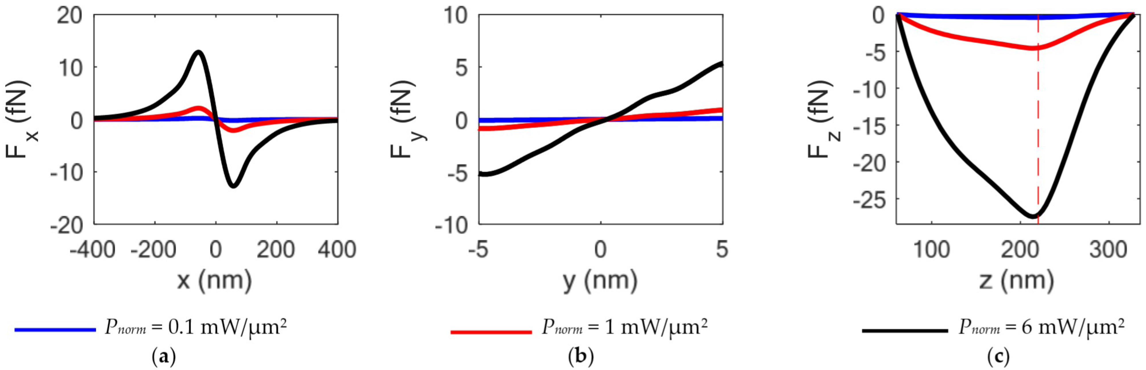
With the bead placed at (x = 0, y = 0), F
z was calculated, observing a linear increase in the optical forces by varying the input power with a peak at z = z
eq = 213.5 nm, close to the top surface of the bowtie. z
eq is the z-coordinate of the equilibrium point, where the field gradients are the largest ones. Optical forces F
x and F
y were calculated by varying the bead position in both axes at z = z
eq. In particular, both forces show symmetry with respect to the position x = x
eq = 0 and y = y
eq = 0, that represent the x- and y-coordinate of the equilibrium point. Along the y-direction, the movement of the bead is limited by the gap g, while along the x-direction, the bead undergoes the optical forces from x = −58 nm to x = +58 nm. For outer values, the bead can be considered free to move. An efficient and stable trapping requires the optical forces to be larger than the repulsive thermal force that could push the particle away from the equilibrium point. The stability of the nanocavity has been estimated as
S =
U/(
kB·Tc), where
U is the potential energy that corresponds to the work required to bring the nanoparticle from a free position to the trapping site [J],
kB is the Boltzmann constant [J/K], and
Tc is the temperature in Kelvin [K], also taking into account the temperature rise due to the trapping effect [
16]. The stability is usually referred to as the potential depth [
46]. An increase in the stability corresponds to a longer trapping time, according to the Kramers theory [
47,
48]. In particular, the trapping time
ttrap is expressed as
. Therefore, the potential energy should be greater than or equal to
kBT. Stability values larger than 1 are required to ensure the dominance of the optical forces with respect to the thermal one, in order to increase the trapping time. A trapping time of several seconds has been observed with other dielectric nanotweezers of
S~1 [
29]. Larger
S values lead to a longer trapping time.
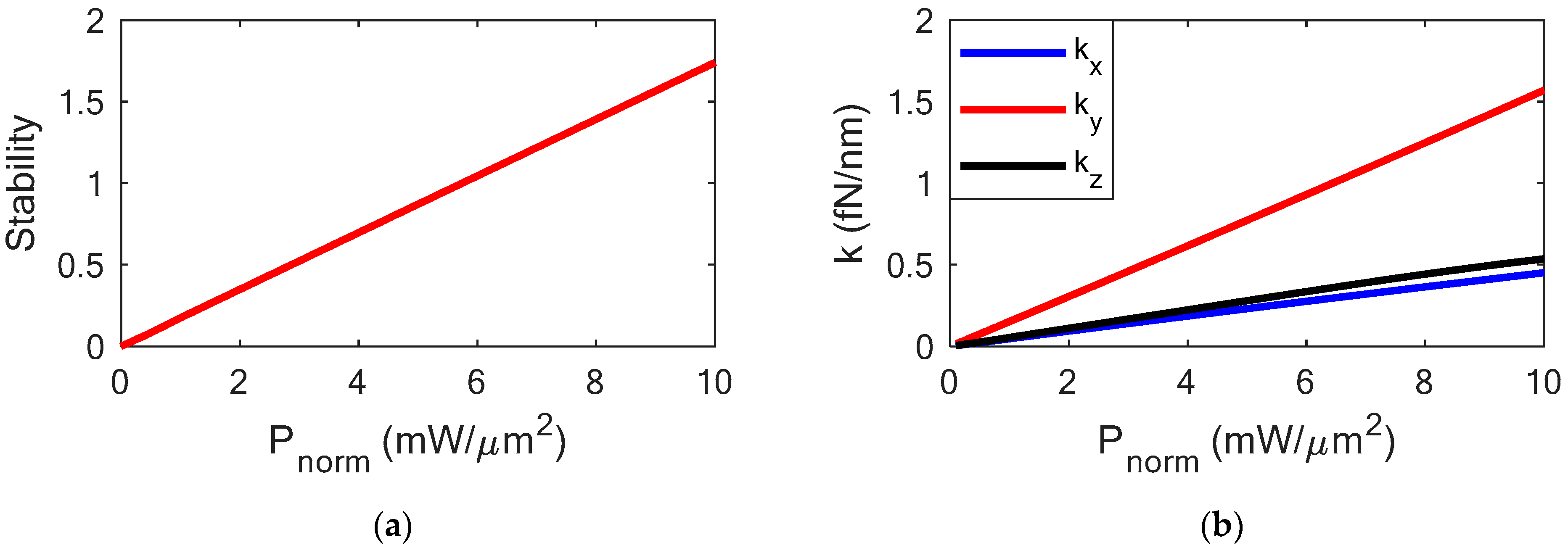
Figure 6a shows the stability of the proposed configuration as a function of the normalized input power. A stability of about 1.2 (potential energy of 1.2 k
BT) has been calculated with an input optical power
Pnorm of 6 mW/µm
2 (
Ptot = 5.77 mW), where F
z shows a peak of 27.45 fN. This performance demonstrates the high stability of a nanoparticle in the trapping site, which corresponds to a long trapping time (tens of seconds), with low input power. However, the experimental demonstration of optical trapping could introduce several physical factors that affect the optical trapping time. In particular, the pointing stability and the power fluctuations of the laser, the resolution of the motion stages, and the environment, in terms of temperature changes, acoustic noise, and mechanical vibrations, are crucial factors for the success of experimental trapping [
9].
To evaluate the trapping stability, the trapping stiffness
ki, expressed as
(i = x, y, z), has been evaluated (
Figure 6b) at the equilibrium point. A high stiffness value ensures a stable position of the particle under test at the equilibrium point. For
Pnorm = 6 mW/ µm
2,
kx = 0.27 fN/nm,
ky = 0.93 fN/nm, and
kz = 0.33 fN/nm have been calculated. The strong electric field confinement along the y-axis leads to the higher value of stiffness.
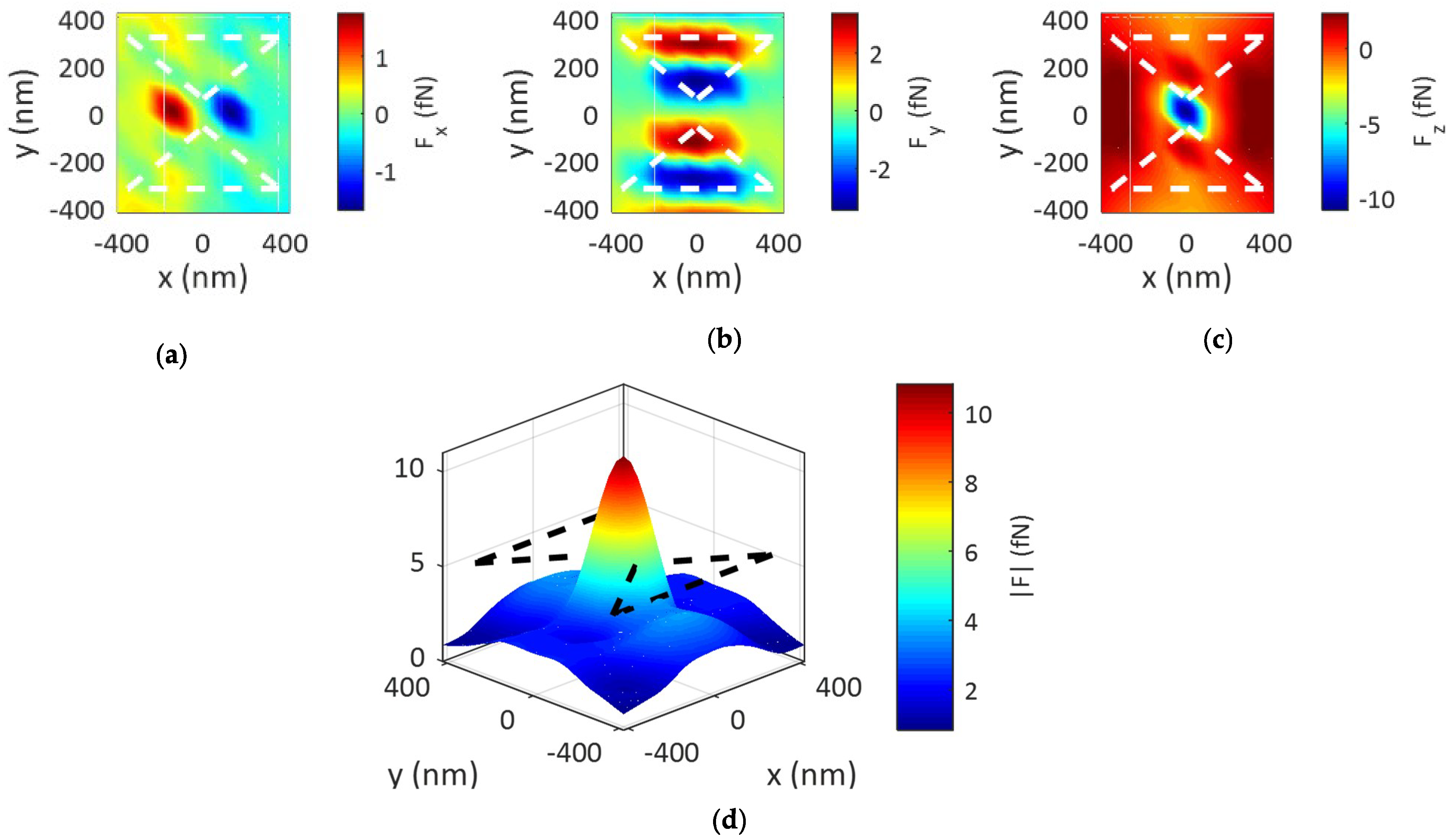
In order to further demonstrate the trapping capability of the designed device, the optical forces have been mapped in the whole device area (
Figure 7). A value of z equal to 275 nm was assumed to ensure the movement of the bead in the x-y plane.
As revealed by the distribution of the force module (
Figure 7d), the slot effect allows the stable trapping of the target particle only in the desired trapping region where the force peak is significant. The symmetrical distribution of the forces F
x and F
y with respect to x = 0 and y = 0, respectively, allows the particle to place itself in the trapping site. Although a direct comparison between the different trapping techniques is difficult due to the dependence of the performance on the particle size, the proposed device shows a stiffness (0.0572 pN/nm/W) significantly higher than other dielectric cavities for trapping (e.g., Z. Xu et al. report 0.0027 pN/nm/W for the trapping of 20 nm bead [
29]), with a significant saving in terms of power (e.g., H. J. Yang et al. report a power of 250 mW for a stable trapping (
S = 10) of 75 nm bead [
49]) and footprint, with respect to the resonant cavities [
11], also preserving the sample temperature, in contrast with the plasmonic nanocavities [
50].
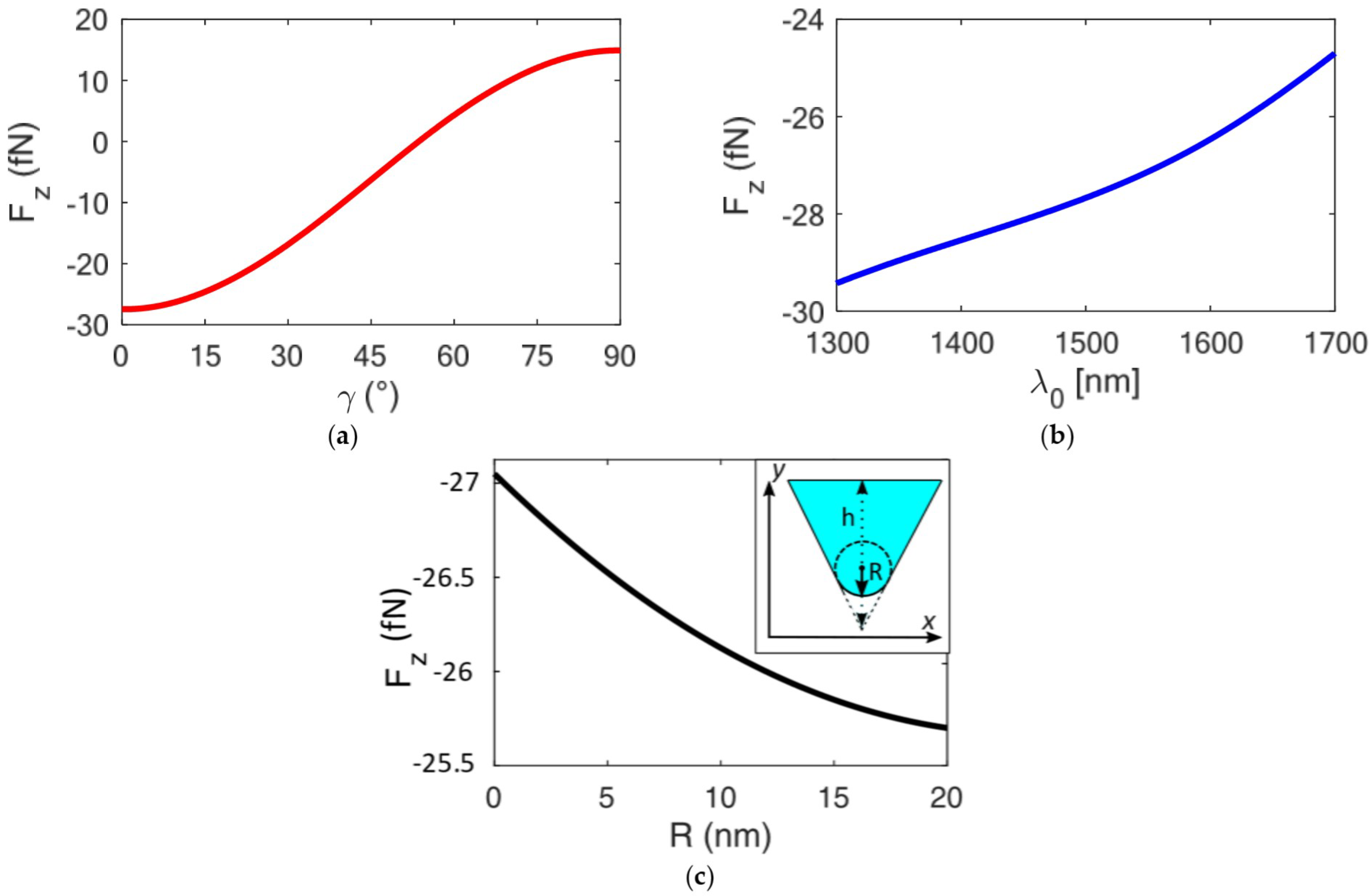
Finally, the robustness of the proposed device with regard to issues on the testing setup, i.e., polarization or operating wavelength change, and fabrication technique, has been investigated.
Figure 8a shows the trend of the optical force F
z at the equilibrium point by varying the polarization direction of the input beam, represented as the angle
γ between the y-axis and the beam. As expected, the optical forces became negligible for
γ = 45° and the bead is repelled from the trapping site for
γ > 45°. The second-order shape of the F
z vs.
γ trend makes the proposed device very robust with respect to the polarization direction: a change in the optical force of less than 10% has been calculated for
γ, ranging from 0° to 15°.
Moreover, the effect of the operating wavelength on the performance was explored by taking into account the material dispersion in terms of refractive index and absorption losses. The trend of the optical forces F
z vs. operating wavelength λ
0 is shown in
Figure 8b. For λ
0 < 1300 nm, the antislot effect arises. As expected, according to the Rayleigh theory [
33], the optical forces increase as the operating wavelength decreases due to the mitigation of the scattering effect. However, although a change in the scattering force of more than 80% is expected within the range 1300–1700 nm, since the scattering force is directly proportional to (1/λ
0)
4, the force gradient attenuates the wavelength dependence.
In fact, an optical force Fz change of ±7% over a range of 400 nm, with respect to λ0 = 1550 nm, has been obtained, with a resulting negligible stability change of about ±0.23. At the same time, this result demonstrates an attenuation of the force dependence by the wavelength and a very high robustness of the device to λ0.
In order to take into account the manufacturing issues that could lead to the rounding of the wedges, the effect of a fillet shape of the wedges has been investigated (see the inset of
Figure 8c). According to the literature [
51], a maximum value of the radius
R = 20 nm has been set. As the radius increases, together with the gap
g, the optical forces decrease, with a maximum change in the force of 5%, which leads to a stability change of 0.16. This behavior is justified by designing the device to improve the mode confinement with a volume region, confirming the strength of the proposed structures to any fabrication issue, in contrast to the behavior of plasmonic tweezers [
16].


