Influence of Gold Nanoantennas on the Photoluminescence of Silicon Nanocrystals


Abstract
:1. Introduction
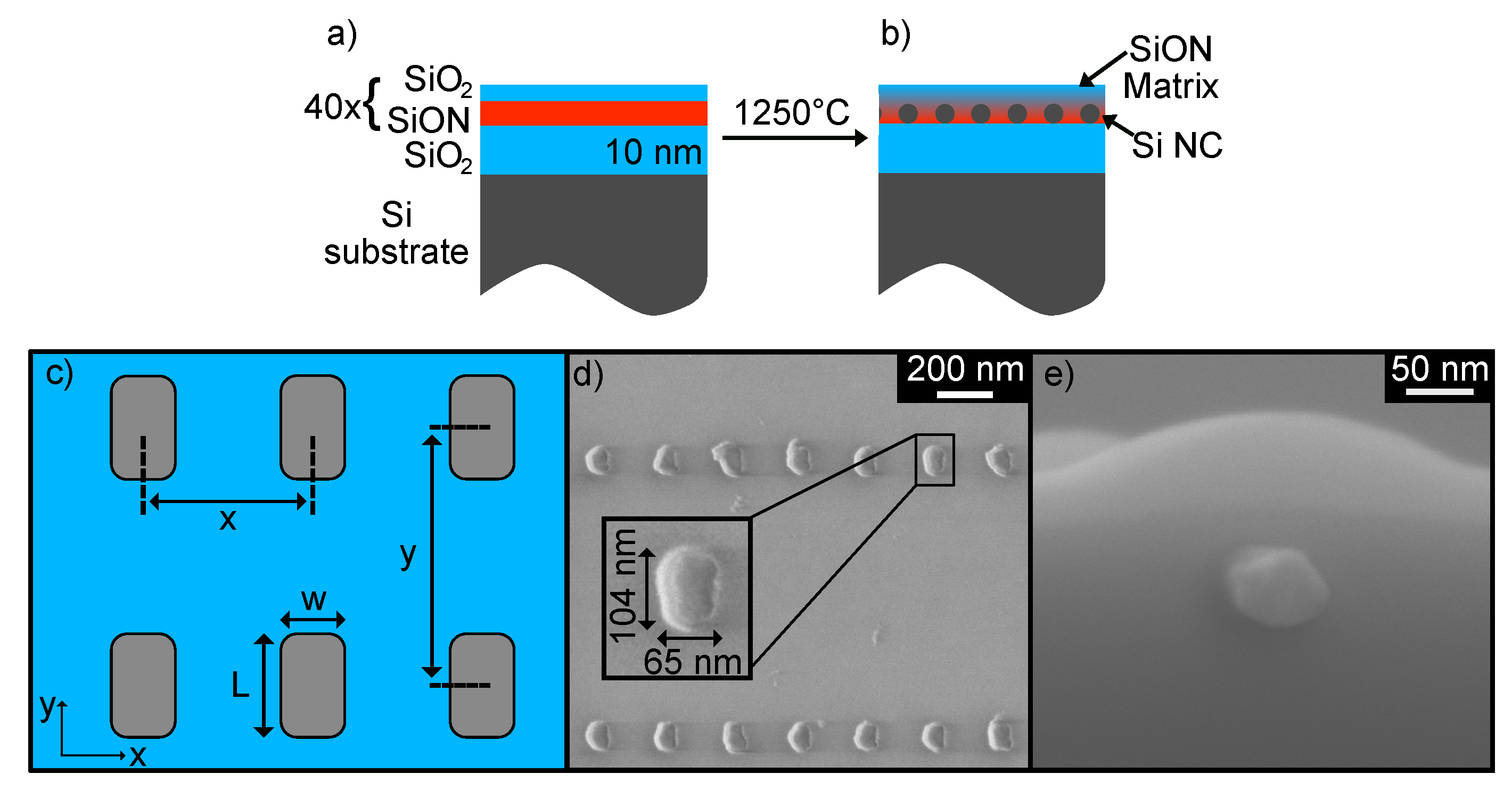
2. Fabrication
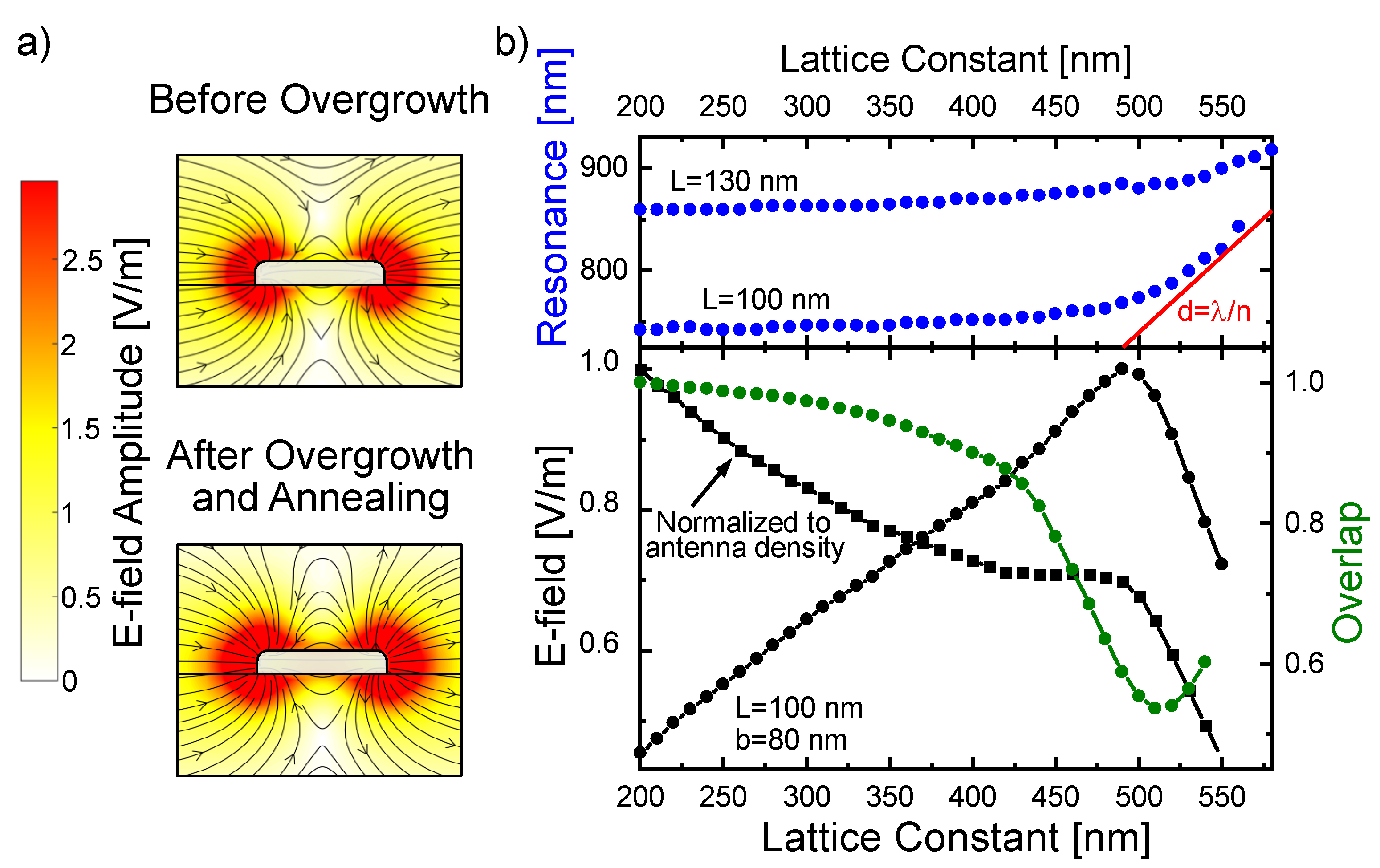
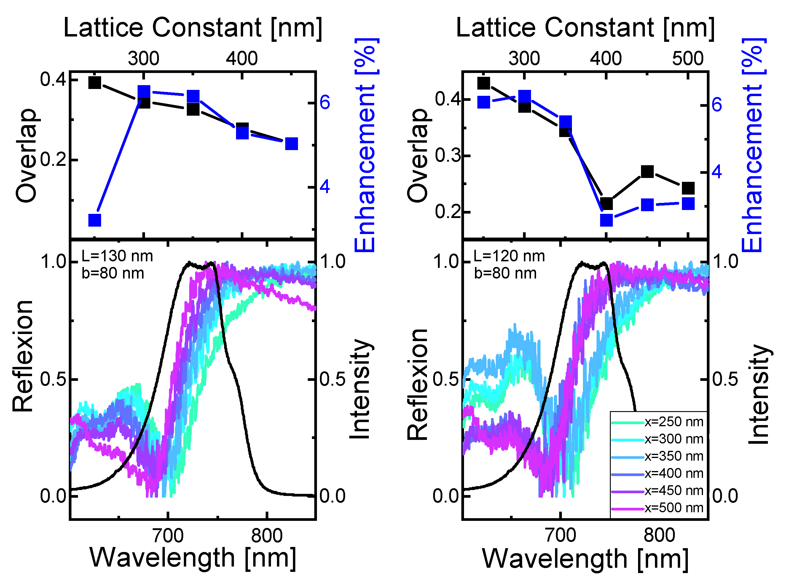
3. Theoretical Results
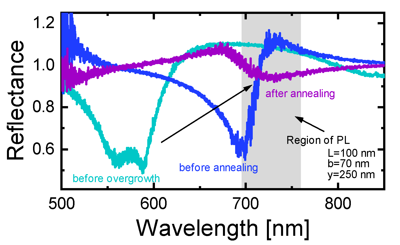
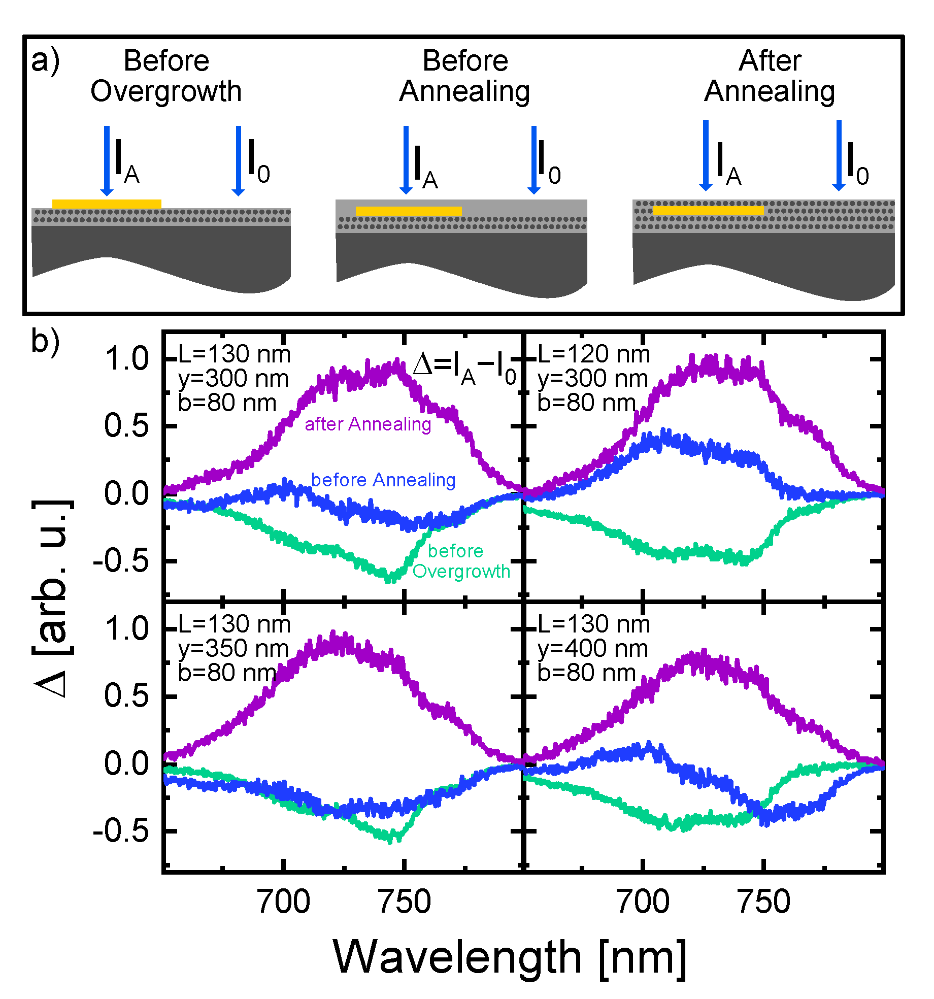
4. Experimental Results
5. Conclusions
Supplementary Materials
Author Contributions
Funding
Institutional Review Board Statement
Informed Consent Statement
Data Availability Statement
Conflicts of Interest
References
- Yates, J.T. A New Opportunity in Silicon-Based Microelectronics. Science 1998, 279, 335–336. [Google Scholar] [CrossRef]
- Marconi, A.; Anopchenko, A.; Pucker, G.; Pavesi, L. Silicon nanocrystal light emitting device as a bidirectional optical transceiver. Semicond. Sci. Technol. 2011, 26, 095019. [Google Scholar] [CrossRef]
- Liu, M.-C.; Chiang, T.-Y.; Kuo, P.-Y.; Chou, M.-H.; Wu, Y.-H.; You, H.-C.; Cheng, C.-H.; Liu, S.-H.; Yang, W.-L.; Lei, T.-F.; et al. SONOS memories with embedded silicon nanocrystals in nitride. Semicond. Sci. Technol. 2008, 23, 075033. [Google Scholar] [CrossRef]
- Zhao, S.; Pi, X.; Mercier, C.; Yuan, Z.; Sun, B.; Yang, D. Silicon-nanocrystal-incorporated ternary hybrid solar cells. Nano Energy 2016, 26, 305–312. [Google Scholar] [CrossRef]
- Liu, C.-Y.; Holman, Z.C.; Kortshagen, U.R. Optimization of Si NC/P3HT Hybrid Solar Cells. Adv. Funct. Mater. 2010, 20, 2157–2164. [Google Scholar] [CrossRef]
- Pi, X.; Zhang, L.; Yang, D. Enhancing the Efficiency of Multicrystalline Silicon Solar Cells by the Inkjet Printing of Silicon-Quantum-Dot Ink. J. Phys. Chem. C 2012, 116, 21240–21243. [Google Scholar] [CrossRef]
- Dal Negro, L.; Pavesi, L.; Pucker, G.; Franzò, G.; Priolo, F. Optical gain in silicon nanocrystals. Opt. Mater. 2001, 17, 41–44. [Google Scholar] [CrossRef]
- Zacharias, M.; Heitmann, J.; Scholz, R.; Kahler, U.; Schmidt, M.; Bläsing, J. Size-controlled highly luminescent silicon nanocrystals: A SiO/SiO2 superlattice approach. Appl. Phys. Lett. 2002, 80, 661–663. [Google Scholar] [CrossRef]
- Meier, C.; Gondorf, A.; Lüttjohann, S.; Lorke, A.; Wiggers, H. Silicon nanoparticles: Absorption, emission, and the nature of the electronic bandgap. J. Appl. Phys. 2007, 101, 103112. [Google Scholar] [CrossRef]
- Belyakov, V.A.; Burdov, V.; Lockwood, R.; Meldrum, A. Silicon Nanocrystals: Fundamental Theory and Implications for Stimulated Emission. Adv. Opt. Technol. 2008, 2008, 279502. [Google Scholar] [CrossRef]
- Hartel, A.M.; Hiller, D.; Gutsch, S.; Löper, P.; Estradé, S.; Peiró, F.; Garrido, B.; Zacharias, M. Formation of size-controlled silicon nanocrystals in plasma enhanced chemical vapor deposition grown SiOxNy/SiO2 superlattices. Thin Solid Films 2011, 520, 121–125. [Google Scholar] [CrossRef]
- Troudi, M.; Sghaier, N.; Souifi, A. Individual silicon nanocrystals photo-current response confirming the quantum single charge residence on single electron nanopixel devices. Phys. E Low-Dimens. Syst. Nanostruct. 2022, 137, 115057. [Google Scholar] [CrossRef]
- Das, P.; Metiu, H. Enhancement of molecular fluorescence and photochemistry by small metal particles. J. Phys. Chem. 1985, 89, 4680–4687. [Google Scholar] [CrossRef]
- Chen, H.; Yang, J.; Rusak, E.; Straubel, J.; Guo, R.; Myint, Y.; Pei, J.; Decker, M.; Staude, I.; Rockstuhl, C.; et al. Manipulation of photoluminescence of two-dimensional MoSe2 by gold nanoantennas. Sci. Rep. 2016, 6, 22296. [Google Scholar] [CrossRef] [PubMed] [Green Version]
- Genov, D.; Sarychev, A.; Shalaev, V.; Wei, A. Resonant Field Enhancements from Metal Nanoparticle Arrays. Nano Lett. 2004, 4, 153–158. [Google Scholar] [CrossRef] [Green Version]
- Leitner, A.; Lippitsch, M.; Draxler, S.; Riegler, M.; Aussenegg, F. Fluorescence properties of dyes adsorbed to silver islands, investigated by picosecond techniques. Appl. Phys. B 1985, 36, 105–109. [Google Scholar] [CrossRef]
- Ritchie, G.; Burstein, E. Luminescence of dye molecules adsorbed at a Ag surface. Phys. Rev. B 1981, 24, 4843–4846. [Google Scholar] [CrossRef]
- Volmert, R.; Weber, N.; Meier, C. Nanoantennas embedded in zinc oxide for second harmonic generation enhancement. J. Appl. Phys. 2020, 128, 043107. [Google Scholar] [CrossRef]
- Köthemann, R.; Weber, N.; Lindner, J.K.N.; Meier, C. High-precision determination of silicon nanocrystals: Optical spectroscopy versus electron microscopy. Semicond. Sci. Technol. 2019, 34, 095009. [Google Scholar] [CrossRef]
- McBrayer, J.D.; Swanson, R.M.; Sigmon, T.W. Diffusion of Metals in Silicon Dioxide. Electrochem. Soc. 1986, 133, 1242–1246. [Google Scholar] [CrossRef]
- Iacona, F.; Franzò, G.; Spinella, C. Correlation between luminescence and structural properties of Si nanocrystals. J. Appl. Phys. 2000, 87, 1295–1303. [Google Scholar] [CrossRef]
- Cushman, C.; Smith, N.; Kaykhaii, M.; Podraza, N.; Linford, M. An introduction to modeling in spectroscopic ellipsometry, focusing on models for transparent materials: The Cauchy and Sellmeier models. Vac. Technol. Coat. 2016, 7, 2–9. [Google Scholar]
- Yakubovsky, D.I.; Arsenin, A.V.; Stebunov, Y.V.; Fedyanin, D.Y.; Volkov, V.S. Optical constants and structural properties of thin gold films. Opt. Express 2017, 25, 25574–25587. [Google Scholar] [CrossRef] [PubMed]
- Maier-Flaig, F. Silizium-Nanokristalle für Optoelektronische Anwendungen, 1st ed.; Karlsruher Institut für Technologie: Karlsruhe, Germany, 2013; pp. 55–59. [Google Scholar]


Publisher’s Note: MDPI stays neutral with regard to jurisdictional claims in published maps and institutional affiliations. |
© 2022 by the authors. Licensee MDPI, Basel, Switzerland. This article is an open access article distributed under the terms and conditions of the Creative Commons Attribution (CC BY) license (https://creativecommons.org/licenses/by/4.0/).
Share and Cite
Köthemann, R.; Golla, C.; Qu, H.; Meier, C. Influence of Gold Nanoantennas on the Photoluminescence of Silicon Nanocrystals. Photonics 2022, 9, 985. https://doi.org/10.3390/photonics9120985
Köthemann R, Golla C, Qu H, Meier C. Influence of Gold Nanoantennas on the Photoluminescence of Silicon Nanocrystals. Photonics. 2022; 9(12):985. https://doi.org/10.3390/photonics9120985
Chicago/Turabian StyleKöthemann, Ronja, Christian Golla, Hong Qu, and Cedrik Meier. 2022. "Influence of Gold Nanoantennas on the Photoluminescence of Silicon Nanocrystals" Photonics 9, no. 12: 985. https://doi.org/10.3390/photonics9120985