Asymmetric Concentric Microring Resonator Label-Free Biosensors


Dpto. de Teoría de la Señal y Comunicaciones e Ingeniería Telemática, Campus Miguel Delibes, Universidad de Valladolid, ETSI Telecomunicación, Paseo de Belén 15, 47011 Valladolid, Spain
Photonics 2022, 9(1), 27; https://doi.org/10.3390/photonics9010027
Submission received: 30 November 2021
/
Revised: 27 December 2021
/
Accepted: 30 December 2021
/
Published: 3 January 2022
(This article belongs to the Special Issue Advances of Silicon Photonics)
Abstract
:A study of label-free silicon nitride asymmetric double-microring resonators is presented. The use of highly accurate 3D vector modal techniques permits an extensive exploration of the parameter space defining the architecture of the proposed device in the search for optimal geometries and reaching configurations not addressed in previous studies that had been limited to symmetrical configurations. Asymmetry, on the other hand, permits to access resonances that exploit the radiation-quenching properties of the structure in an optimal way. The analysis presented also includes the effect of absorption in the sensor aqueous cladding that is generally omitted. The results of the numerical survey indicate that the optimized geometries bring about a substantive performance improvement at small microring radii that are impractical for more conventional single-ring geometries due to the high radiation losses. Therefore, lower footprint devices, and a larger scale of integration, can be attained with the proposed structure.
1. Introduction
Integrated biological and chemical sensors permit the label-free detection of analytes by the evanescent field sensing of changes in the refractive index of the waveguide surrounding medium that, in turn, modify the guided mode effective index [1,2,3]. Microring structures fabricated in CMOS-integrated silicon photonics platforms are particularly appealing, since the resonance effect permits the enhancement of the sensitivity of reduced footprint devices.
Amongst the CMOS-compatible photonics integration platforms, silicon nitride is an attractive option for the implementation of optical biosensors [4,5,6] because of several advantages over the more extensively used silicon platform: it has a lower intrinsic linear propagation loss, its large band gap results both in the absence of nonlinear loss due two-photon absorption and in transparency in the visible and NIR spectral regions and, also, its reduced thermo-optic coefficient provides better stability against temperature fluctuations. Furthermore, the silicon nitride platform is not only compatible with CMOS fabrication processes, but also most of the surface functionalization protocols [5].
The refractive index of silicon nitride is relatively large, but smaller than that of silicon. A lower refractive index in the integrated waveguide core means that a poorer field confinement is obtained. The reduced field confinement results in a larger sensitivity to refractive index variations of the cladding that can be very interesting for sensing applications. On the other hand, the effect of radiation losses due to the waveguide curvature becomes more pronounced and, consequently, the bent radii have to be increased in relation to those of silicon integrated circuits in order to obtain low losses and sharp resonances. In [7,8,9], the use of asymmetric coupled waveguides for the reduction of radiation losses in curved structures and its application to the enhancement of the intrinsic Q-factor of racetrack micro-resonators was studied in depth. These guiding geometries have been proven particularly useful for the reduction of the footprint of silicon nitride devices. Furthermore, the acute differential losses for TE and TM polarizations in these structures have been exploited in the fabrication of ultracompact integrated polarizers [10,11].
The sharpening of the resonant response in symmetric coupled microrings have previously been noted in [12] and studied using a coupled-resonator model. Biosensors based on concentric microresonators in the symmetric case were analyzed in [13,14,15]. Whereas the coupled-resonator model is necessary for describing the operation of nonconcentric rings [16,17], the modal method used in [8,9,10,11] provides a more direct approach in concentric arrangements. This technique provides a very large degree of accuracy, necessary in the design of devices to be incorporated in fabricated photonic chips [9,11], at a low computational cost. These combined features permit the optimization of more general asymmetric structures not previously addressed. At the same time, the effect of propagation losses due to absorption in the aqueous cladding can be easily incorporated to the analysis. Biosensors based on pulley-type resonators have also been studied in [18]. These structures permit the reduction of radiation losses by wrapping the ring with the access waveguide. Nevertheless, coupling and radiation reduction properties become entangled, which complicates the optimization of the structures.
In this work, we present a thorough analysis of the properties of optical biosensors built using asymmetric concentric double-ring structures. Following our previous works on racetrack microresonators [7,8,9], we seek to exploit the radiation-quenching properties of the exterior waveguide leading to solutions clearly distinct from those of symmetric structures. The mechanism employed is based on the impact of an asymmetric coupled waveguide on the mode field distribution of a curved dielectric channel. When the field distribution in the proposed geometry is compared to that of the isolated main waveguide, we observe the existence of specific values of the design parameters that provide an improved confinement of the optical field inside the main waveguide. In these cases, the exterior waveguide acts as an efficient shielding against the effects of radiation. It is noteworthy that the best-case solutions rest in broad regions in the optimization parameter plane where performance variations are smooth, resulting in designs that are resilient against fabrication tolerances [9,10,11].
2. Fundamentals
There are two distinct operation mechanisms that can be employed for the evanescent sensing of the surrounding medium using microring resonators [1]. In homogeneous sensing devices, a variation of the concentration of a biochemical analyte produces a modification of the refractive index of the cover medium. In the surface-sensing mechanism, on the other hand, the refractive index change results from the modification of the receptor molecules localized at a functionalized ultrathin layer at the microring interface. The modeling of surface sensing is highly dependent on the properties of each specific application. For the sake of generality, in this work, we focus on the homogeneous sensing case for the systematic analysis of the properties of concentric asymmetric microring resonators label-free biosensors. The most general conclusions of the analysis are expected to apply as well, when extrapolated to surface-sensing devices.
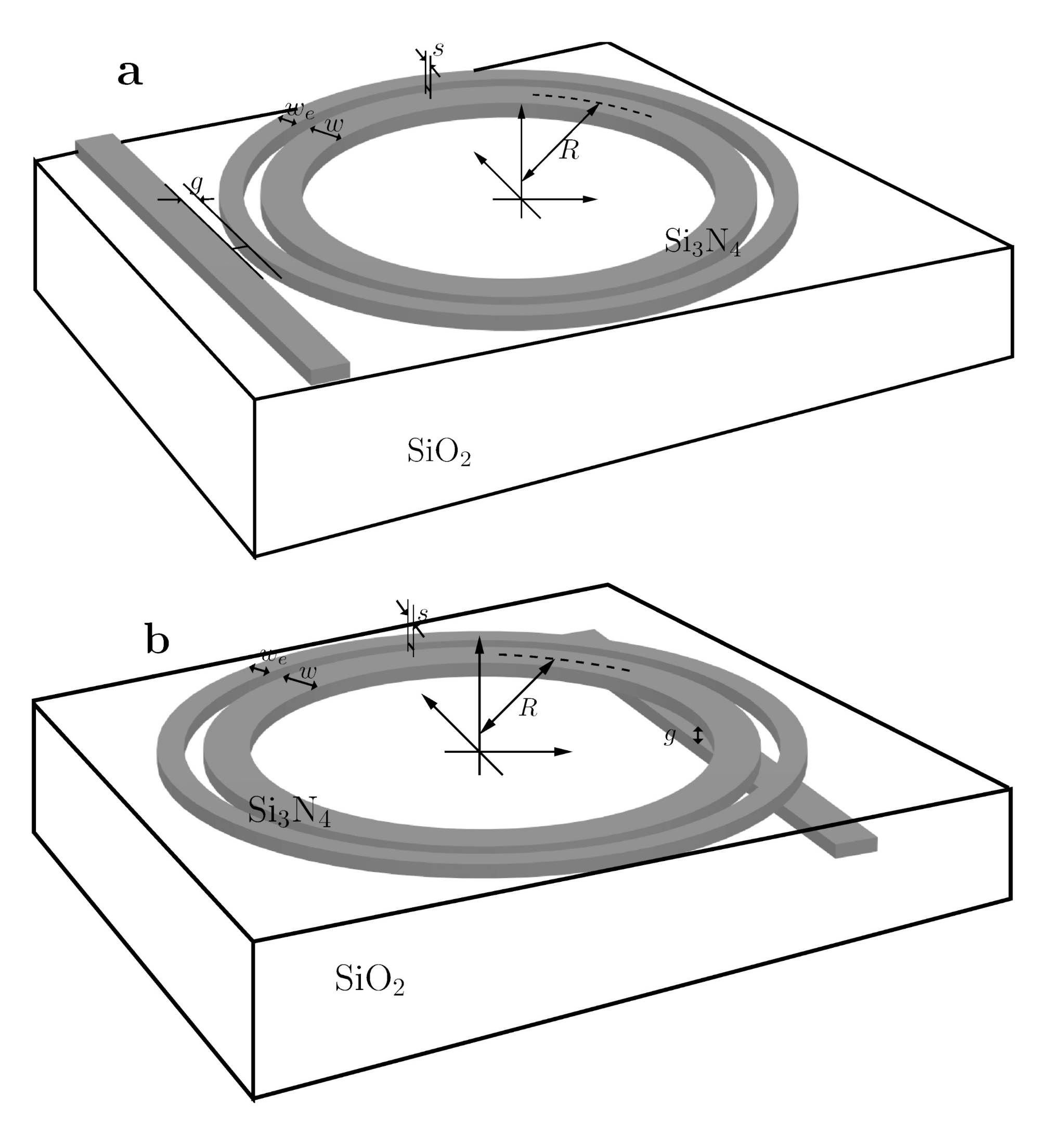
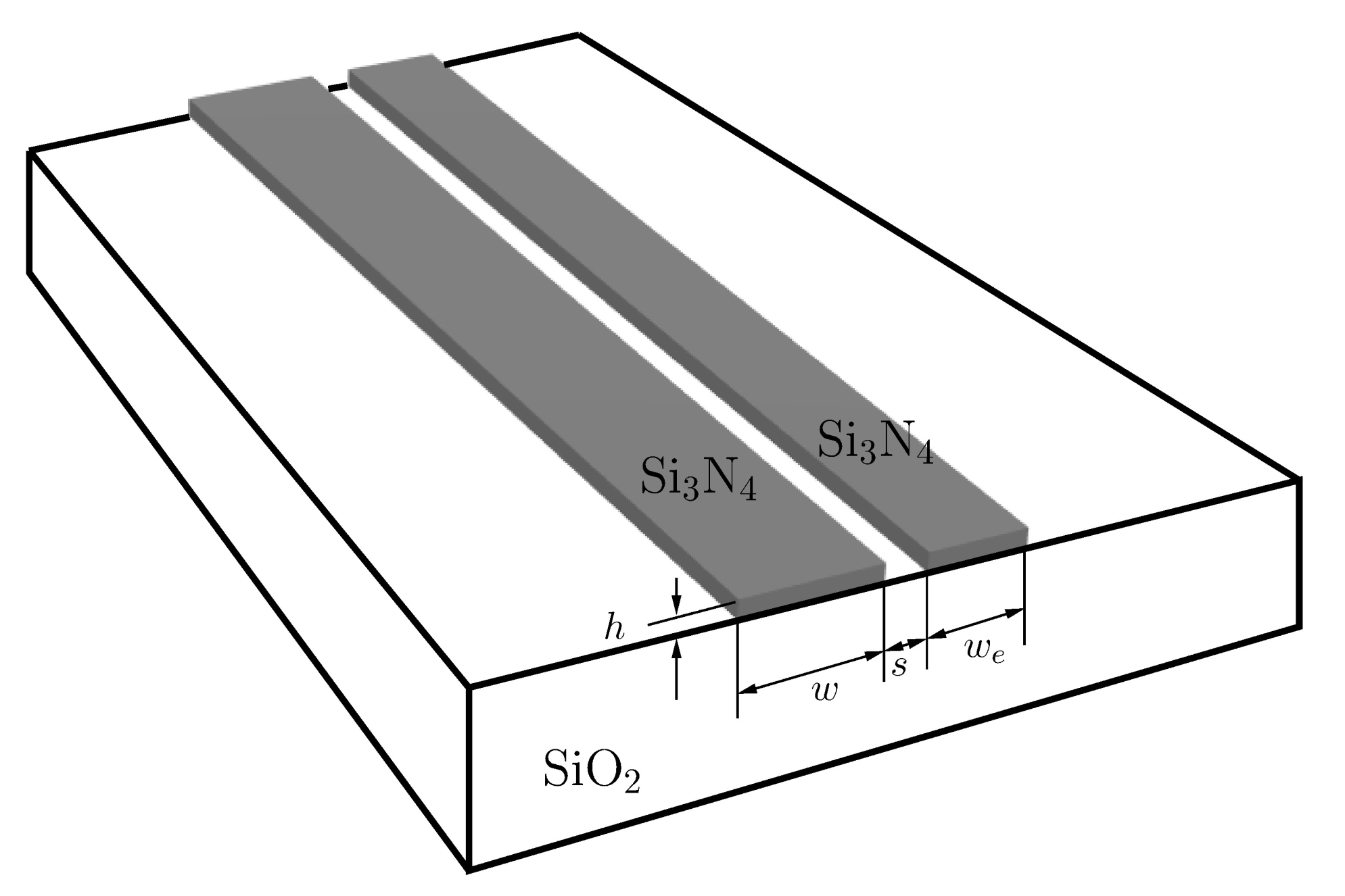
Figure 1 displays the geometry of the silicon nitride microring sensors analyzed in this work. The rectangular waveguides lie on top of a layer grown over the silicon wafer. The microring is placed at the sensing region, within a trench opened in the top cover so as to be accessible to the analyte in an aqueous solution delivered to the sensor through a microfluidic arrangement. The reference cover medium is water and our analyses include the effect of the absorption in the sensor surrounding medium. We use the waveguide geometry of [7,8,9,10,11], typical of the silicon nitride platform. The height h (see Figure 2) of the silicon nitride waveguides takes as fixed value of 300 nm and the width of the inner microring waveguide will always be 1 μm. In the following, we call this optical channel the main waveguide of the system. The design parameters that we vary in order to optimize our structures are the width of the outermost waveguide , the waveguide separation s, and the radius of the curvature R measured at the center at the innermost waveguide. For the calculations, we use the same values for the bulk refractive indices at nm of , , and , , as in [9,11], and we set the refractive index and extinction coefficient of water as and , respectively [19].
Figure 1 also shows an access straight waveguide that is part of the sensor readout optical circuit and that is coupled to the microresonator at a minimum distance point with gap separation g. There are two possible arrangements [20]: side or vertical coupling, illustrated in panels a and b of Figure 1, respectively. In either case, parameter g determines the coupling coefficient t [2]. This coupling coefficient is most relevant to the overall system response, and together with the internal propagation loss, determines the Q-factor of the resonator [2]. There are pros and cons to each of the two coupling arrangements of Figure 1 [20], but some of the advantages of vertical coupling are particularly outstanding when microrings are used in biosensing applications. First, it permits an efficient coupling between the access and the main ring waveguides that exploits in an effective manner the radiation-quenching mechanism described in [7,8,9]. Furthermore, the changes in the cover medium during the sensor operation would affect the coupling properties in a side-coupled structure making the analysis more complex and introducing an additional variable to the optimization design. We seek low intrinsic loss configurations preserving the phase matching to the access waveguide in a lossy cover medium. In this case, using a vertical coupling approach permits us to consider that coupling conditions are essentially unaffected by the other system parameters and to focus on the propagation properties of the modal fields in the structure for the optimization of the devices. Furthermore, the analysis presented in this work, focused on the propagation properties intrinsic to the microring structure, remains equally valid in the case of alternative conformations such as an add-drop configuration [3], which is also commonly found in this type of sensors and permits the design of more elaborate sensing systems [6].
Nonconcentric double (or multiple) ring structures [16,17] are well-suited to a coupled resonator analysis [12,17] but a design oriented toward device fabrication requires more involved numerical techniques for the solution of the full 3D vector Maxwell equations in arbitrary guiding geometries, such as FDTD [21], in order to fulfill the accuracy specifications. On the other hand, concentric structures, either symmetric or asymmetric, are most efficiently studied using highly accurate modal techniques. We base our numerical investigations on a finite-difference scheme valid for curved waveguiding structures [22], implemented in the WGMS3D software package [23] that permits the inclusion of lossy materials in the guiding geometry. This allows us to take into consideration the effect of the water propagation loss. This highly relevant effect is most often ignored in the analyses.
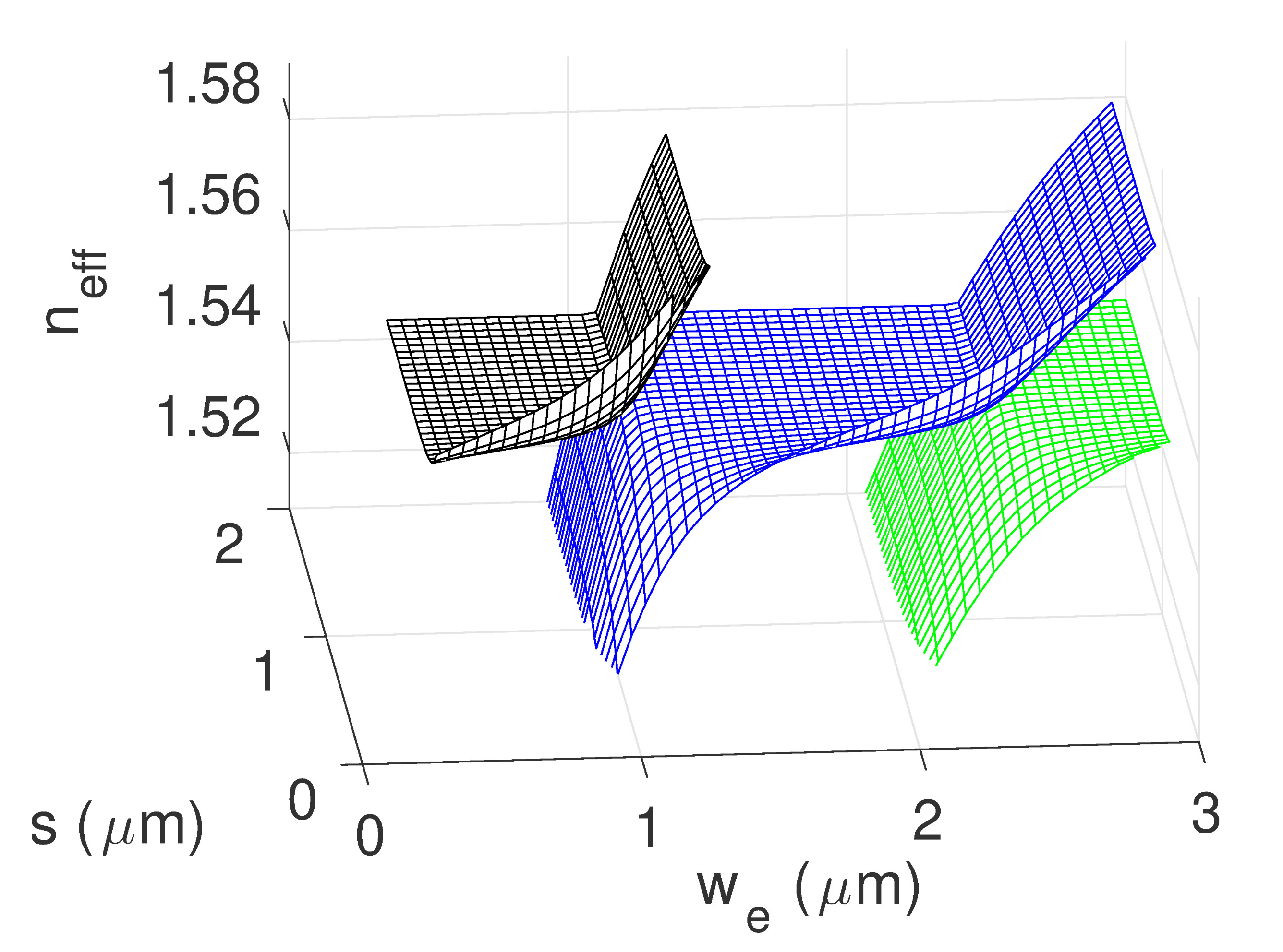
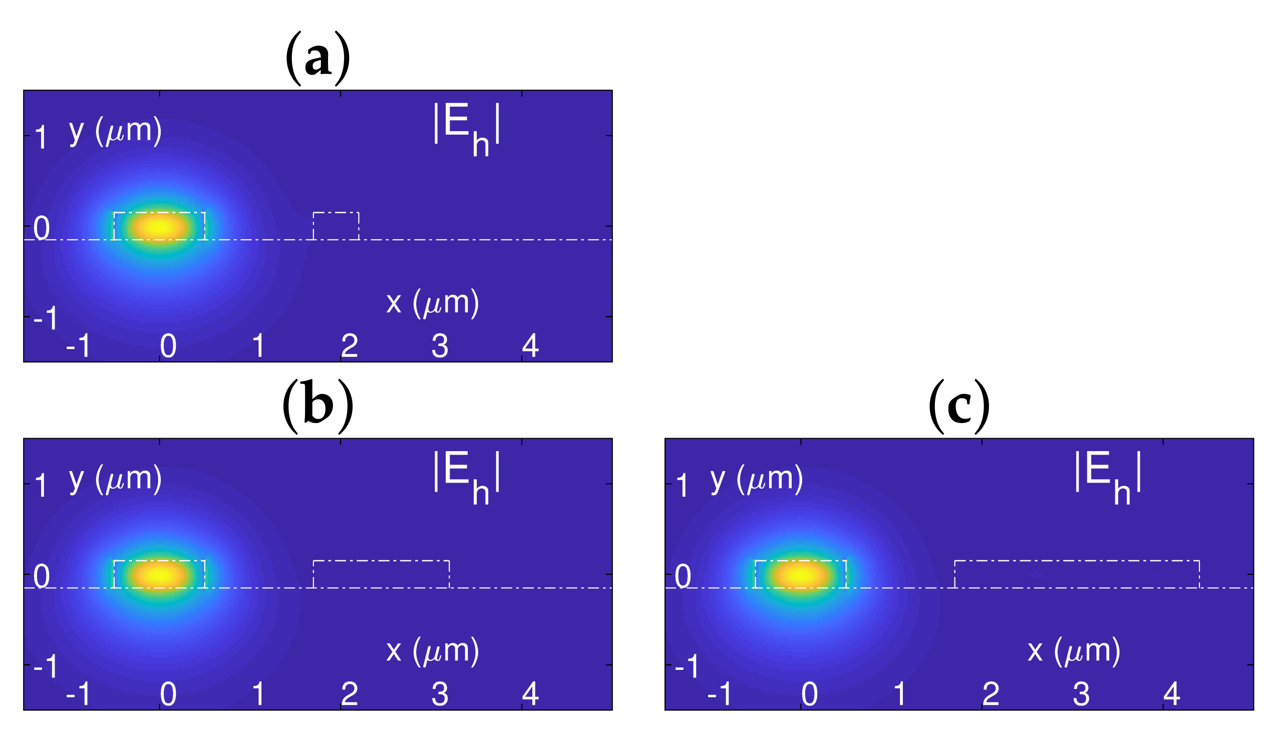
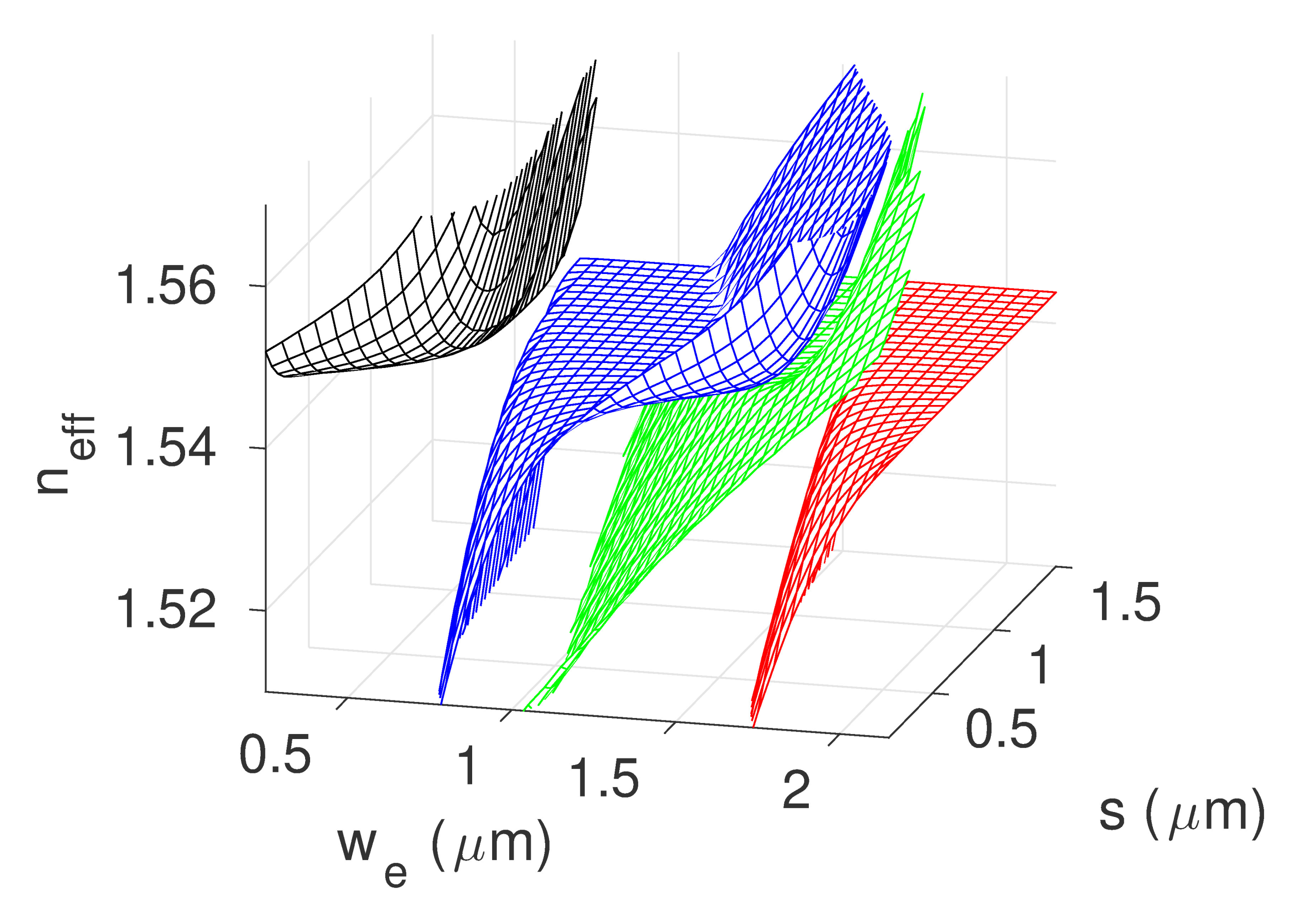
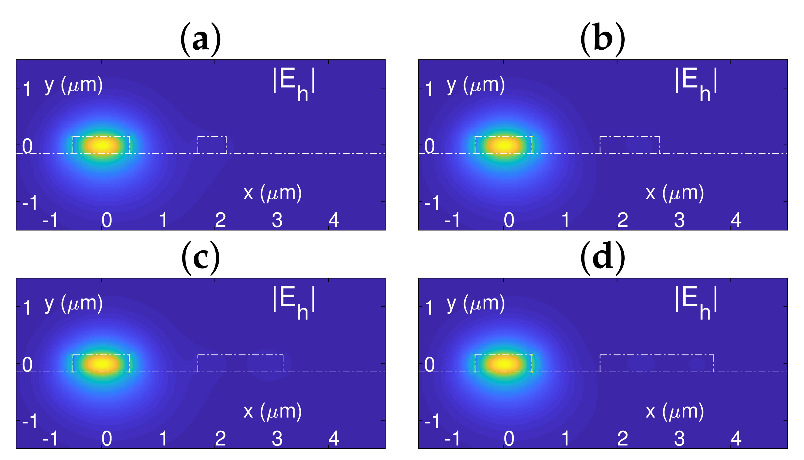
The way the propagation characteristics change when the design parameters are modified are best understood if we start by analyzing the straight () asymmetric coupled waveguides displayed in Figure 2. The values of the effective indices of the modes guided in the structure as a function of and s are depicted in Figure 3 for the TE-polarized solutions. The line defines a straight symmetric coupler. For large waveguide separation , and , the system supports two degenerate modes each of them localized at one of the waveguides. As s decreases and the two identical waveguides come closer together, the mode coupling becomes stronger and the degeneracy disappears: the coupler now supports two (super) modes, with respective odd and even symmetry, and with distinct effective indices; the differences in the effective indices grow as s becomes smaller. The effective indices of these two modes can be continued in the (,s) plane and they define two respective noncrossing sheets. As one moves out of the line, in the asymmetric case, and for sufficient waveguide separation s, there exists a broad region lying close to the plane (with the effective index of the isolated main waveguide) at both sides of the boundary for each of the two modes. In either case, the mode whose sheet is in close proximity to the plane has its energy predominantly confined in the main waveguide. As is further increased, we can observe that a third mode emerges, and becomes the one that is mainly confined in the main waveguide for larger values of . For each value of and s, we call the principal mode the one that has an effective index closest to that of the single waveguide structure. As the difference between these two values becomes smaller, the mode confinement in the main waveguide becomes progressively tighter. The transverse electric field strength amplitude for three principal modes at each of the modal sheets of Figure 3 are illustrated in Figure 4. In all three cases, we observe that the solution is highly localized at the main waveguide of the structure. The properties of these solutions are in high contrast with those of a symmetric coupler, where the modal fields of the two modes supported are equally distributed between the two waveguides.
When a dielectric waveguide is bent to a finite radius R, forming a ring structure, the modal solutions transform into quasi-modes with complex propagation constants that reflect the presence of losses due to radiation [24]. In the following, we will also refer to the real part of the complex effective index of the mode as effective index. Figure 5 illustrates the impact on the TE modal effective indices when the straight geometry of Figure 2 is bent to a radius of R = 50 μm. First, there is a shift of the effective index in the curved isolated main waveguide. This reflects in a corresponding shift of the flat support of the modal solution predominantly confined in the main waveguide for each value of and s (principal mode) [11]. At the same time there is a clear distortion of the boundaries separating the regions at which each modal sheet is tangent to the single waveguide flat support. This reflects the effective deformation of the waveguide index profile along the radial direction induced by the curvature [24].
Within the domains where the modal sheets become nearly tangent to the isolated main waveguide support, one finds that the modal field distribution experiences a lesser coupling to the radiation tail, resulting in regions with reduced radiation losses [7,8,9] and our target will be the optimal solutions, in the sense of the lowest radiation loss, lying in these domains. These optimal solutions are out of reach in a symmetric concentric ring design, where the value of would take a fixed value of μm. The properties of the distribution of the electric field strength amplitude of the principal mode solutions are illustrated in Figure 6. The high degree of confinement of these solutions in the principal inner ring permit us to obtain a design with an optimal reduction of the radiation loss, and largely improved performance in relation to that of a single-ring structure.
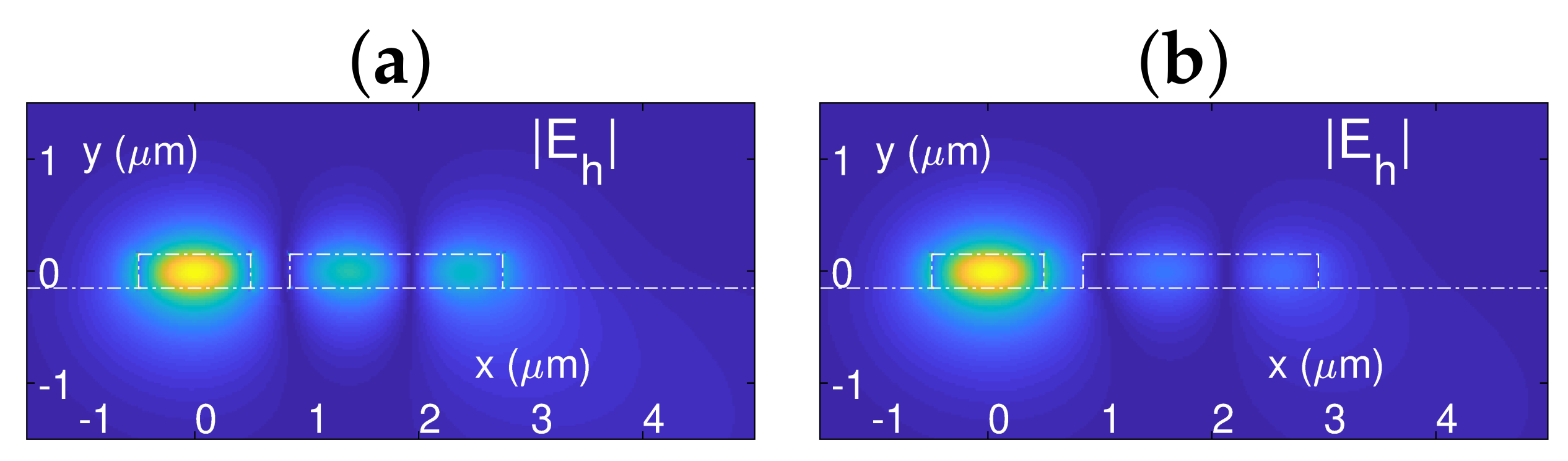
It is noteworthy that when Figure 3 and Figure 5 are compared, one observes, for R = 50 μm, a bifurcation of the boundary close to μm and the emergence of a new modal solution. Figure 7 displays, for a separation of μm, the respective transverse electric field strength distributions of two modes belonging to the third and fourth sheets of Figure 5 that bifurcate, due to the waveguide bending, from the third sheet of Figure 3. For this smaller value of s, the deviation of the effective indices relative to that of the mode in the uncoupled main waveguide is larger, the modal field is less confined inside the main waveguide, and the details of the field distributions over the outer waveguide can be clearly distinguished. We can see that the field distributions of the two bifurcated modes are, in fact, very similar, even though they differ in the number of nulls inside the outer waveguide core, a clear signature of having a different mode order.
In a ring microresonator, resonances appear at each wavelength where the round-trip phase accumulated by the propagating optical field is an integer multiple of , that is,
where . The frequency separation between resonances (free spectral range) is inversely proportional to R. The shape of the resonances is determined both from round-trip signal attenuation, defining the round-trip amplitude factor , the coupling coefficient t between the access waveguide and the resonator, and it is best captured in the Q-factor [2]
with , assuming an ideal (lossless) coupling. is the group index
Similar results apply in the case of a two-coupler add-drop configuration, with
assuming identical values of coefficient R characterizing both couplings.
The operation of the biosensor requires the determination of a spectral shift in the filter response produced by a change in the refractive index of the cover medium. Under typical operation conditions, the mode effective index, and therefore the resonance wavelength, displays a linear variation with the refractive index of the cover medium. Thus, we evaluate the sensitivity of the device by introducing a small change in the refractive index of water. This procedure is in line with related studies, e.g., [18]. In the following, we will also assume that nm.
The readout of the sensor output requires an accurate determination of the resonance wavelength in the presence of noise. The performance of the algorithms employed for this task improve as the dip at resonance becomes more acute [5]. The full width at half-maximum (FWHM) spectral width of the resonance line is directly related to the Q factor [2] as
and so the detection efficiency increases with the value of Q. In Equation (4), the value of R can be arbitrarily tailored as part of the design process. a is a more delicate parameter that depends on the mode propagation properties and it is a limiting factor for the accessible values of Q. Therefore, our optimization strategy will focus on the value of a in order to maximize the Q factor by effectively quenching the radiated field.
3. Results
3.1. Single-Ring Si3N4 Resonators with an Aqueous Cover
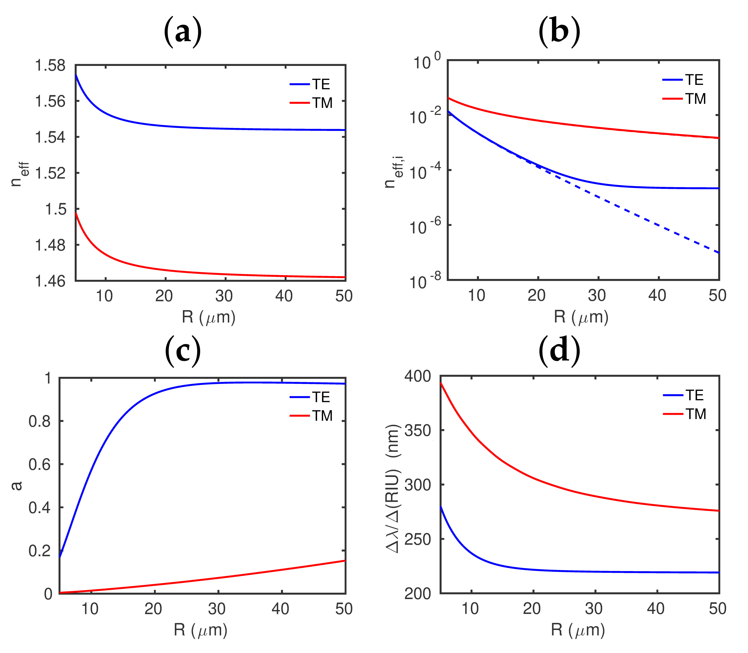
The results for the TE and TM polarized modes in a single ring structure as a function of R are shown in Figure 8. The real part of the complex effective indexes are shown in panel (a). The TM mode is less confined in the waveguide core. This results in a higher sensitivity (panel (d)) to changes in the top cladding when operating as a sensor, but also in larger radiation losses. The quantification of radiation loss can be performed using the values of the imaginary part of the complex effective index shown in panel (b) that have been calculated including the effect of absorption in water. In order to evaluate the relative impact of the two loss effects, absorption and radiation, the values calculated when the absorption in water is neglected are also plotted with dashed lines. When the two curves overlap, we obtain evidence that the effect of the correction due to the attenuation in water is negligible. In the case of the TM-polarized field, propagation loss is clearly dominated by radiation effects for all values of R. In the case of a TE field, on the contrary, radiation loss dominates for bent radii up to approximately μm and absorption for larger values of R.
The results from Figure 8d show substantially larger values of sensitivity when the TM field is employed, as expected from the looser field confinement in the waveguide core. Nevertheless, an analysis of the round-trip amplitude values displayed in Figure 8c indicates that the Q-factor is too small to obtain usable devices with TM-polarized field. As regards the TE-polarized mode, values of ring radii larger than , in the region limited by water absorption, give values of a closer to 1, sufficient for a usable response.
3.2. Asymmetric Concentric Ring Resonators
Asymmetric concentric coupled waveguides in racetrack microresonators have previously been tested as an effective way to reduce radiation loss, particularly in silicon nitride devices [7,9]. We now explore the performance of these structures for asymmetric concentric ring resonator sensors. For this purpose, we systematically search the region spanning the lower order modal sheets in the (,s) plane where optimal geometries are expected. Ring separations between 150 and 1500 nm and exterior ring widths with values from 250 to 2200 nm were initially considered, both ranges sampled at 50 nm intervals. The upper bound of the separation values addressed was increased to 1850 nm for values of R of 40 and 50 μm, since the optimal values were outside the initially defined range.
3.2.1. TE-Polarized Field
Figure 9 and Figure 10 display, respectively, the round-trip amplitude factor and the sensitivity of the TE-polarized principal mode for six different values of R. As previously stated, the principal mode is, at each point in the plane, the one closest to the flat support defined by the value of in the main waveguide at the corresponding R. The values of and s that give the largest value of a for each R are marked with a black spot in each figure.
The boundaries of the domains defining the transitions of which mode becomes the principal one can be easily identified in Figure 9 by the large values of attenuation. It can be observed in Figure 9 that the attenuation decreases as we move towards the central positions of these domains. Even though the effect can be observed at all values of R, it becomes more pronounced as R decreases and the radiation losses clearly dominate over the water absorption loss. It is also noteworthy that the characteristics of the bifurcation of the modal sheet spotted in Figure 5 for μm change with the value of R, and the bifurcation eventually disappears for sufficiently small R.
If we focus on the central positions of these domains, the values of the sensitivities displayed in Figure 10 show a similar tendency to that of Figure 8d, for a single ring, with very mild variations unless R is decreased to very small values, where significant improvements can be obtained. At these strong curvatures, nevertheless, the values of a diminish notably, resulting in very poor Q-factors. The inclusion of the asymmetric concentric external ring, on the other hand, permits to improve the round-trip amplitude factor, that now can take values in excess of even for values of R as small as μm.
The reduction of the microring radius permitted by the proposed asymmetric double-ring structure provides both an enhancement of the Q-factor and the sensitivity, an increase of the free spectral range (FSR) [2]
and a substantial reduction in the device footprint.
The main results of the numerical survey are summarized in Table 1. It is interesting to note that even though the imaginary part of the modal effective index decreases monotonically with R, the values of the transmission factor a display a slight decrease at μm that is due to the effect of the enlargement of the propagation distance with R. The optimized structures display an improvement in the value of a relative to that of the single-ring geometry for all the values of R studied. What is more relevant is that this improvement becomes larger as the value of R diminishes. Therefore, the proposed geometry permits the implementation of biosensors with substantially reduced dimensions. The last two columns of Table 1 display the values of and s providing an optimal response. We highlight that these optimal values are, in general, at a significant distance from the value μm defining the symmetric case, especially for the more interesting cases of low values of R. The calculated values of the sensitivity, as shown in Table 1, are larger than in other silicon nitride microring resonator biosensors, e.g., 49 and nm/RIU in [4,5], respectively, even though the last figure corresponds to a very conservative estimate of the device performance [4].
3.2.2. TM-Polarized Field
Results for the TM case were also studied for completeness. Figure 11 and Figure 12 display, respectively, the round-trip amplitude factor and the sensitivity of the TM-polarized principal mode for six different values of R and the optimal results are summarized in Table 2. In line with the results observed for a single-ring structure, the looser confinement of the TM mode field results in much larger values of the sensitivity. Again, the round-trip field amplitude factor is too small for practical applications, but we can observe a significant improvement of the round-trip amplitude factor. Our results are limited by a large aspect ratio, which is typical of some silicon nitride foundries. Nevertheless, these results suggest that the combination of a less extreme aspect ratio of the rectangular waveguides combined with an asymmetric concentric microring geometry may result in the TM mode fields being a usable alternative for the implementation of biosensors with improved sensitivity.
4. Conclusions
A comprehensive numerical study of silicon nitride optical biosensors based on asymmetric double-ring microresonators was presented. The results showed an improved performance of the optimized geometries that permitted the design of devices with substantially reduced dimensions. The optimization criterion used, leading to minimal propagation losses, was based on a search performed over modal fields that were tightly confined within the inner ring, called the principal mode in this work, which offered a significantly reduced radiation loss. These are in sharp contrast with previously studied symmetric double-ring microresonator sensing devices, with field distributions evenly distributed over the two rings. Furthermore, the optimal geometries were found at significant distances from the symmetrical dispositions. In order to perform this analysis, we employed an eigensolver capable of finding modes in curved geometries that was highly accurate and computationally efficient when compared with other techniques. These combined properties permitted an extensive systematic search over the optimization domain. Furthermore, absorption losses in the aqueous cover, most often neglected, was included in the analysis.
Although the conclusions of this work apply mainly to devices operating with TE-polarized fields, the properties of devices based on TM polarization have also been addressed. The lower confinement of the TM modes provides an increase of the sensitivity at the cost of an attenuation that is too large for practical implementations in spite of the substantive increase of the amplitude transmission factor provided by a double asymmetric microring design. It is important to stress that this limitation is a consequence of the extreme aspect ratio of the silicon nitride waveguides typical of some photonics integration platforms. Nevertheless, as the ecosystem of open-access silicon nitride platforms grows [25], widely different values of this aspect ratio are becoming available, bringing into the design of optical biosensors an additional degree of freedom and new possibilities.
Funding
This research was funded by Ministerio de Ciencia e Innovación grant number PID2020-119418GB-I00 and Junta de Castilla y León grant number VA296P18.
Institutional Review Board Statement
Not applicable.
Informed Consent Statement
Not applicable.
Data Availability Statement
Not applicable.
Conflicts of Interest
The authors declare no conflict of interest.
References
- Chao, C.-Y.; Guo, L.J. Design and Optimization of Microring Resonators in Biochemical Sensing Applications. J. Lightwave Technol. 2006, 24, 1395–1402. [Google Scholar] [CrossRef]
- Bogaerts, W.; De Heyn, P.; Van Vaerenbergh, T.; De Vos, K.; Selvaraja, S.K.; Dumon, P.; Bienstman, P.; Van Thourhout, D.; Baets, R. Silicon microring resonators. Laser Photonics Rev. 2012, 6, 47–73. [Google Scholar] [CrossRef]
- De Vos, K.; Bartolozzi, I.; Schacht, E.; Bienstman, P.; Baets, R. Silicon-on-Insulator microring resonator for sensitivie and label-free biosensing. Opt. Express 2007, 15, 7610–7615. [Google Scholar] [CrossRef] [PubMed]
- Das, S.; Samudrala, S.C.; Lee, J.J.; Abdallah, M.G.; Wenner, B.R.; Allen, J.W.; Allen, M.S.; Magnusson, R.; Vailyev, M. Si-N-Microring-Resonator-Based Optical Biosensor for Neuropeptide Y Detection. IEEE Photon. Technol. Lett. 2021, 33, 888–891. [Google Scholar] [CrossRef]
- Ghasemi, F.; Hosseini, E.S.; Song, X.; Gottfried, D.S.; Chamanzar, M.; Raeiszadeh, M.; Cummings, R.D.; Eftekhar, A.A.; Adibi, A. Multiplexed detection of lectins using integrated glycan-coated microring resonators. Biosens. Bioelectron. 2016, 80, 682–690. [Google Scholar] [CrossRef] [Green Version]
- Wang, J.; Yao, Z.; Poon, A.W. Silicon-nitride-based integrated optofluidic biochemical sensors using a coupled-resonator optical waveguide. Front. Mater. 2015, 2, 34. [Google Scholar] [CrossRef] [Green Version]
- Chamorro-Posada, P. Q-Enhanced racetrack microresonators. Opt. Commun. 2017, 387, 70–78. [Google Scholar] [CrossRef] [Green Version]
- Chamorro-Posada, P. Radiation in bent asymeetric coupled waveguides. Appl. Opt. 2019, 58, 4450–4457. [Google Scholar] [CrossRef]
- Chamorro-Posada, P.; Baños, R. Design and Characterization of Q-Enhanced Silicon Nitride Racetrack Micro-Resonators. J. Lightw. Technol. 2021, 39, 2917–2923. [Google Scholar] [CrossRef]
- Chamorro-Posada, P. Ultracompact integrated polarizers using bent asymmetric coupled waveguides. Opt. Lett. 2019, 44, 2040–2043. [Google Scholar] [CrossRef]
- Chamorro-Posada, P. Designa and characterization of silicon nitride ultracompact integrated polarizers using bent asymmetric coupled waveguides. Opt. Lett. 2021, 46, 609–612. [Google Scholar] [CrossRef]
- Zhang, Z.; Dainese, M.; Wosinski, L.; Qiu, M. Resonance-splitting and enhanced noctch depth in SOI ring resonators with mutual mode coupling. Opt. Express 2008, 16, 4621–4630. [Google Scholar] [CrossRef]
- Li, X.; Su, Y.; Zhang, Z.; Qiu, M.; Qin, S. Label-free biosensor based on silicon-on-insulator concentric micro-ring resonators. In Proceedings of the 2008 IEEE PhotonicsGlobal@Singapore, Singapore, 8–11 December 2008; pp. 1–3. [Google Scholar]
- Li, X.; Zhang, Z.; Qin, S.; Wang, T.; Liu, F.; Qiu, M.; Su, Y. Sensitive label-free and compact biosensor based on concentric silicon-on-insulator microring resonators. Appl. Opt. 2009, 48, F90–F94. [Google Scholar] [CrossRef] [PubMed]
- Sun, L.; Yuan, J.; Ma, T.; Sang, X.; Yan, B.; Wang, K.; Yu, C. Design and optimization of silicon concentric dual-microring resonators for refractive index sensing. Opt. Commun. 2017, 395, 212–216. [Google Scholar] [CrossRef]
- Zhang, L.; Song, M.; Wu, T.; Zou, L.; Beausoleil, R.G.; Willner, A.E. Embedded ring resonators for microphotonic applications. Opt. Lett. 2008, 33, 1978–1980. [Google Scholar] [CrossRef] [PubMed]
- Su, B.; Wang, C.; Kan, Q.; Chen, H. Compact Silicon-on-Insulator Dual-Microring Resonator Optimized for Sensing. J. Lightw. Technol. 2011, 29, 1535–1541. [Google Scholar]
- Malmir, K.; Habibiyan, H.; Ghafoorifard, H. Ultrasensitive optical biosensors based on microresontors with bent waveguides. Optik 2020, 216, 164906. [Google Scholar] [CrossRef]
- Hale, G.M.; Querry, M.R. Optical constants of water in the 200-nm to 200-μm wavelength region. Appl. Opt. 1973, 12, 555–563. [Google Scholar] [CrossRef]
- Chin, M.K.; Ho, S.T. Design and Modeling of Waveguide-Coupled Single-Mode Microring Resonators. J. Lightw. Technol. 1998, 16, 1433–1446. [Google Scholar] [CrossRef] [Green Version]
- Yee, K. Numerical solution of initial boundary value problems involving Maxwell’s equations in isotropic media. IEEE Trans. Antennas Propag. 1966, 14, 302–307. [Google Scholar]
- Krause, M. Finite-difference mode solver for curved waveguides with angled and curved dielectric interfaces. J. Light. Technol. 2009, 29, 691–699. [Google Scholar] [CrossRef]
- wgms3d-Full-Vectorial Waveguide Mode Solver. Available online: http://www.soundtracker.org/raw/wgms3d/ (accessed on 16 November 2021).
- Hiremath, K.R.; Hammer, M.; Stoffer, R.; Prkna, L.; Ctyroky, J. Analytic approach to dielectric optical bent slab waveguides. Opt. Quantum Electron. 2005, 37, 37–61. [Google Scholar] [CrossRef]
- Rahim, A.; Goyvaerts, J.; Szelag, B.; Fedeli, J.-M.; Absil, P.; Aalto, T.; Harjanne, M.; Littlejohns, C.; Reed, G.; Winzer, G.; et al. Open-Access Silicon Photonics Platforms in Europe. IEEE J. Select. Top. Quantum Electron. 2019, 25, 8200818. [Google Scholar] [CrossRef] [Green Version]
Figure 1.
Concentric nonsymmetric microring-sensing geometry displaying (a) side coupling and (b) bottom coupling to the access waveguide.
Figure 1.
Concentric nonsymmetric microring-sensing geometry displaying (a) side coupling and (b) bottom coupling to the access waveguide.

Figure 2.
Geometry of silicon nitride straight asymmetric coupled waveguides with an aqueous cover used for reference purposes. System parameters are also annotated in the figure and defined in the text.
Figure 2.
Geometry of silicon nitride straight asymmetric coupled waveguides with an aqueous cover used for reference purposes. System parameters are also annotated in the figure and defined in the text.

Figure 3.
Effective indices of the TE modes propagating in the straight coupled asymmetric structure of Figure 2 as the two design parameters and s are varied. Three modes can be observed in the (,s) range depicted in the figure.
Figure 3.
Effective indices of the TE modes propagating in the straight coupled asymmetric structure of Figure 2 as the two design parameters and s are varied. Three modes can be observed in the (,s) range depicted in the figure.

Figure 4.
Amplitudes of the horizontal main field components of the TE modes propagating in the straight coupled asymmetric structure of Figure 2. The plots correspond to the respective modal sheets of Figure 3, each of them lying on the plane defined by the effective index of the isolated main waveguide (principal modes). Plots (a–c) are for the same value of μm and respective values of of , and μm. The waveguide boundaries are outlined with a white dashed line.

Figure 5.
(Real part of the) effective indices of the TE quasi-modes propagating in the asymmetric concentric two-ring structure of Figure 1 as the two design parameters and s are varied. Four quasi-modes can be observed in the (,s) range depicted in the figure.
Figure 5.
(Real part of the) effective indices of the TE quasi-modes propagating in the asymmetric concentric two-ring structure of Figure 1 as the two design parameters and s are varied. Four quasi-modes can be observed in the (,s) range depicted in the figure.

Figure 6.
Amplitudes of the horizontal main electric field components of the TE modes propagating in the asymmetric concentric microring structure of Figure 1 with R = 50 μm. The plots correspond to the respective modal sheets of Figure 5, each of them lying on the plane defined by the effective index of the isolated main waveguide (principal mode). Plots (a–d) are for the same value of μm and respective values of of , , and μm. The waveguide boundaries are outlined with a dashed white line.

Figure 7.
Amplitudes of the horizontal main electric field components of the TE modes propagating in the asymmetric concentric microring structure of Figure 1 with R = 50 μm. The plots correspond to the third (green) and fourth (red) sheets, respectively, in that figure. Plots (a,b), are for the same value of μm and respective values of of and μm. The waveguide boundaries are outlined with a dashed white line.

Figure 8.
Results from the computations for a single-ring structure: variation of (a) the real part of the complex modal effective index, (b) the imaginary part of the complex modal effective index, (c) the round-trip field amplitude factor a and (d) the sensitivity , as a function of R and at nm. Results for the TE- and TM-polarized mode are shown with blue and red solid lines, respectively. Dashed lines in panel (b) correspond to the results obtained when the effect of absorption in water is neglected.

Figure 9.
Round-trip field amplitude factor of the principal TE mode for six different values of R: 15 μm, 20 μm, 25 μm, 30 μm, 40 μm and 50 μm at nm, as a function of the design parameters and s. Maximal values of a are indicated with a black dot in the figure.
Figure 9.
Round-trip field amplitude factor of the principal TE mode for six different values of R: 15 μm, 20 μm, 25 μm, 30 μm, 40 μm and 50 μm at nm, as a function of the design parameters and s. Maximal values of a are indicated with a black dot in the figure.

Figure 10.
Sensitivity ( of the principal TE mode for six different values of R: 15 μm, 20 μm, 25 μm, 30 μm, 40 μm and 50 μm at nm, as a function of the design parameters and s. The positions corresponding to the maximal values of a are marked with black spots.
Figure 10.
Sensitivity ( of the principal TE mode for six different values of R: 15 μm, 20 μm, 25 μm, 30 μm, 40 μm and 50 μm at nm, as a function of the design parameters and s. The positions corresponding to the maximal values of a are marked with black spots.

Figure 11.
Round-trip field amplitude factor of the principal TM mode for six different values of R: 15 μm, 20 μm, 25 μm, 30 μm, 40 μm and 50 μm at nm, as a function of the design parameters and s. The positions corresponding to the maximal values of a are marked with black spots.
Figure 11.
Round-trip field amplitude factor of the principal TM mode for six different values of R: 15 μm, 20 μm, 25 μm, 30 μm, 40 μm and 50 μm at nm, as a function of the design parameters and s. The positions corresponding to the maximal values of a are marked with black spots.

Figure 12.
Sensitivity ( of the principal TM mode for six different values of R: 15 μm, 20 μm, 25 μm, 30 μm, 40 μm and 50 μm al nm, as a function of the design parameters and s. The positions corresponding to the maximal values of a are marked with black spots.
Figure 12.
Sensitivity ( of the principal TM mode for six different values of R: 15 μm, 20 μm, 25 μm, 30 μm, 40 μm and 50 μm al nm, as a function of the design parameters and s. The positions corresponding to the maximal values of a are marked with black spots.


Table 1.
Single-ring round-trip transmission amplitude factor a and sensitivity S and the corresponding values for optimal (Opt.) asymmetric concentric ring geometries for six values of R. The parameters defining the optimized structures, and s, are also shown in the table. Results are for the TE-polarized mode.
| Radius | Single-Ring a | Opt. a | Single-Ring S | Opt. S | Opt. | Opt. s |
|---|---|---|---|---|---|---|
| (μm) | (nm/RIU) | (nm/RIU) | (μm) | (μm) | ||
| 15 | ||||||
| 20 | ||||||
| 25 | ||||||
| 30 | ||||||
| 40 | ||||||
| 50 |
Table 2.
Single-ring round-trip transmission amplitude factor a and sensitivity S and the corresponding values for optimal (Opt.) asymmetric concentric ring geometries for six values of R. The parameters defining the optimized structures, and s, are also shown in the table. Results are for the TM-polarized field.
| Radius | Single-Ring a | Opt. a | Single-Ring S | Opt. S | Opt. | Opt. s |
|---|---|---|---|---|---|---|
| (μm) | (nm/RIU) | (nm/RIU) | (μm) | (μm) | ||
| 15 | ||||||
| 20 | ||||||
| 25 | ||||||
| 30 | ||||||
| 40 | ||||||
| 50 |
Publisher’s Note: MDPI stays neutral with regard to jurisdictional claims in published maps and institutional affiliations. |
© 2022 by the author. Licensee MDPI, Basel, Switzerland. This article is an open access article distributed under the terms and conditions of the Creative Commons Attribution (CC BY) license (https://creativecommons.org/licenses/by/4.0/).
Share and Cite
MDPI and ACS Style
Chamorro-Posada, P. Asymmetric Concentric Microring Resonator Label-Free Biosensors. Photonics 2022, 9, 27. https://doi.org/10.3390/photonics9010027
AMA Style
Chamorro-Posada P. Asymmetric Concentric Microring Resonator Label-Free Biosensors. Photonics. 2022; 9(1):27. https://doi.org/10.3390/photonics9010027
Chicago/Turabian StyleChamorro-Posada, Pedro. 2022. "Asymmetric Concentric Microring Resonator Label-Free Biosensors" Photonics 9, no. 1: 27. https://doi.org/10.3390/photonics9010027
Note that from the first issue of 2016, this journal uses article numbers instead of page numbers. See further details here.