Recent Progress of Electrically Pumped AlGaN Diode Lasers in the UV-B and -C Bands


Abstract
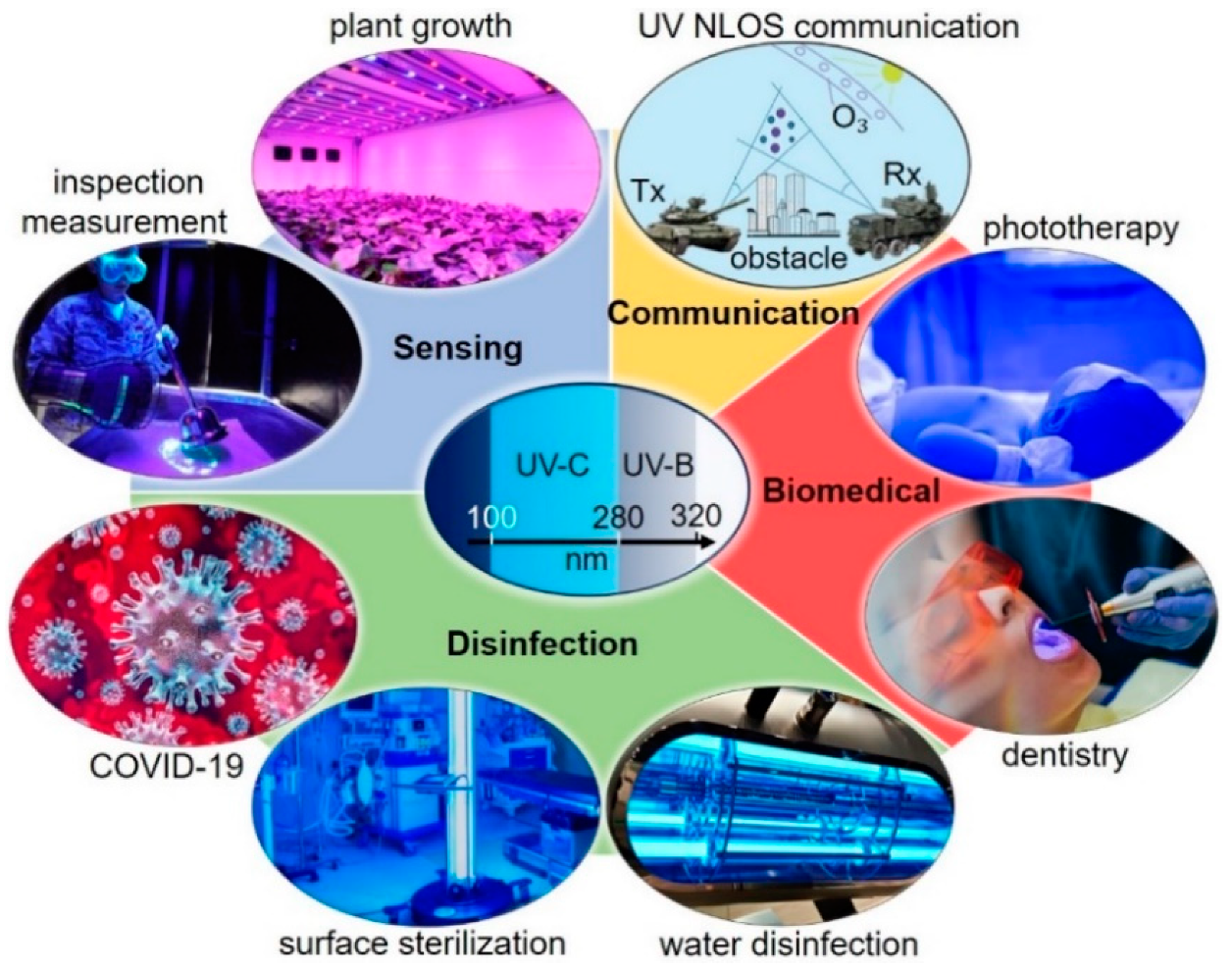
:1. Introduction
2. Overview of Recent Progress of AlGaN Ultraviolet (UV)-B and -C Lasers
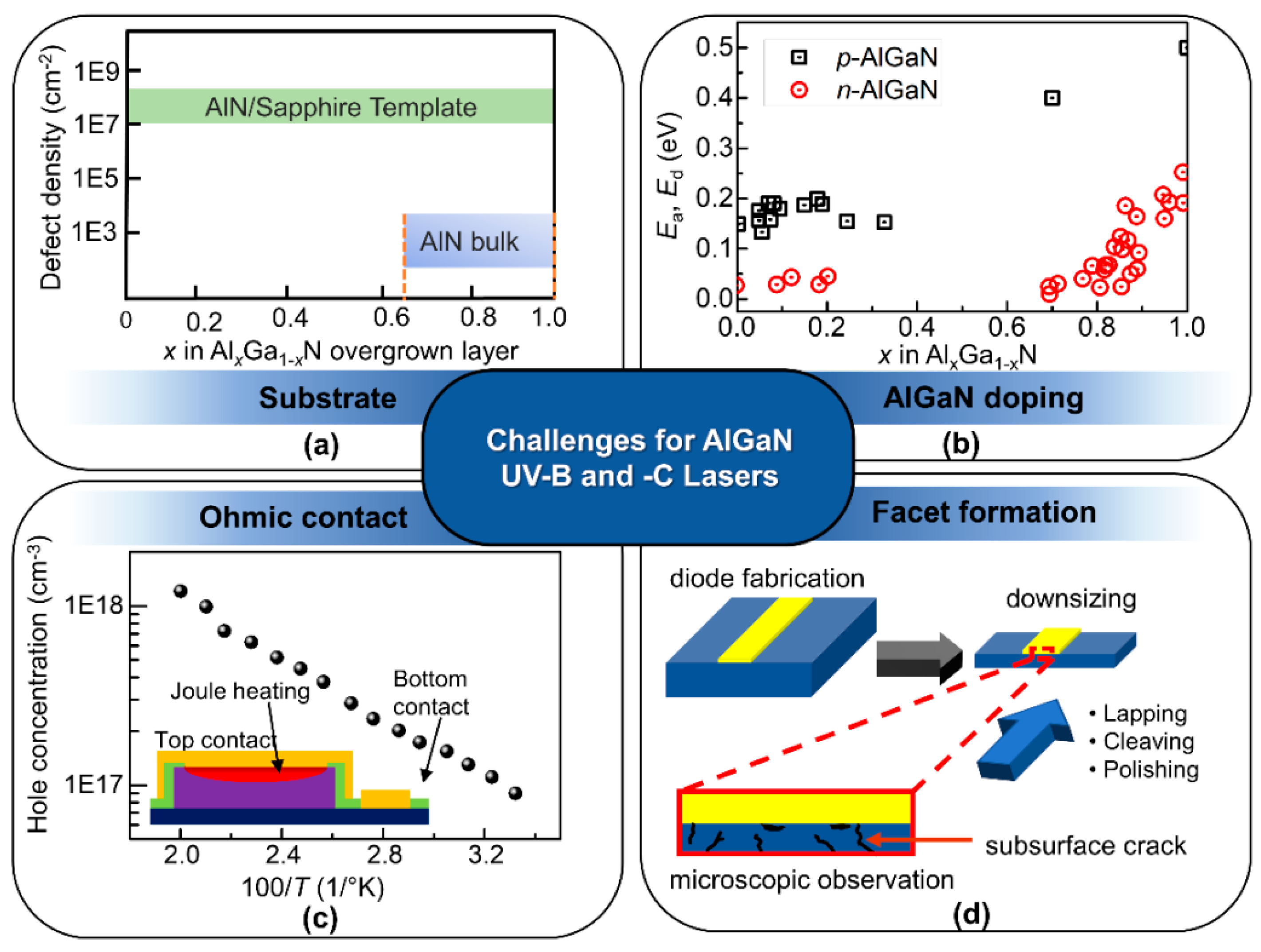
3. Challenges of AlGaN UV-B/C Lasers
3.1. Substrates and Defects
3.2. P- and N-Doping for High-Al
3.3. Low-Resistive Ohmic Contact
3.4. Facet Formation
4. Critical Technical Areas for AlGaN UV-B and -C Lasers
4.1. Substrate Materials
4.1.1. Substrates for UV-C Lasers
4.1.2. Substrates for UV-B Lasers
4.1.3. Silicon Substrates for Nanowire Lasers
4.2. Growth Technology
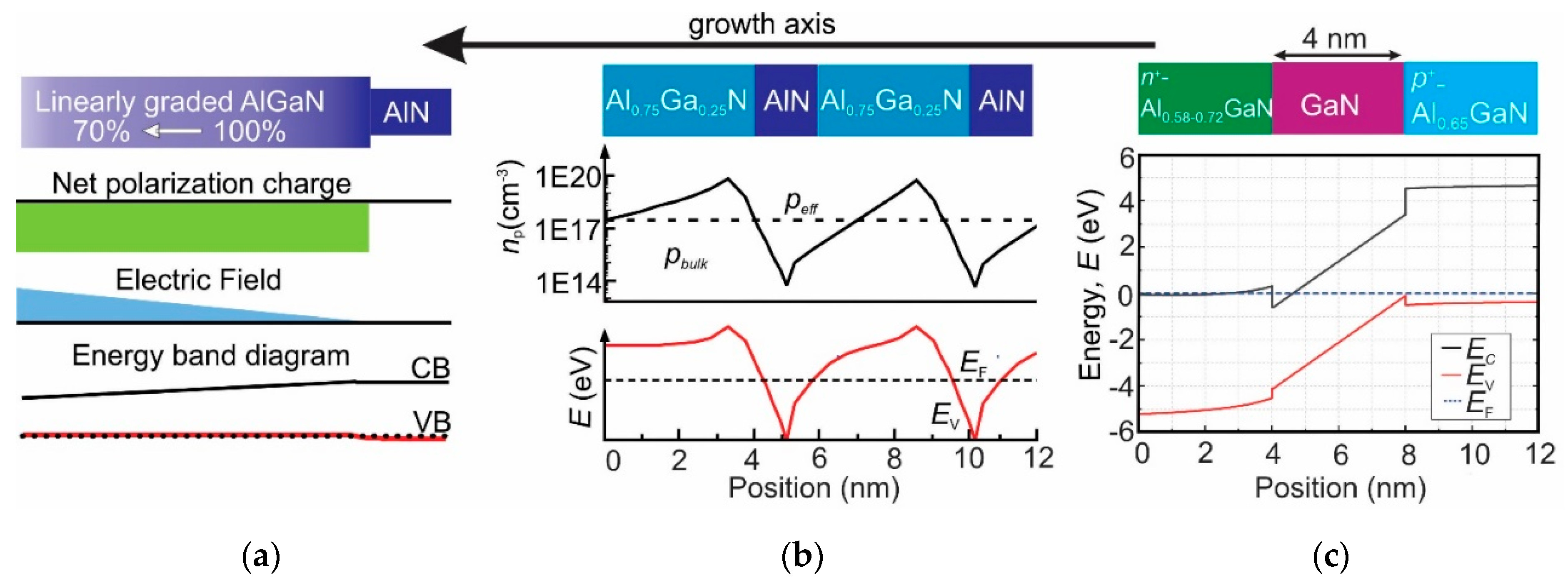
4.3. Three Major Techniques for Hole Injection
4.3.1. Distributed Polarization Doping
4.3.2. Short-Period Superlattice
4.3.3. Tunnel Junctions (TJs)
4.4. Active Region
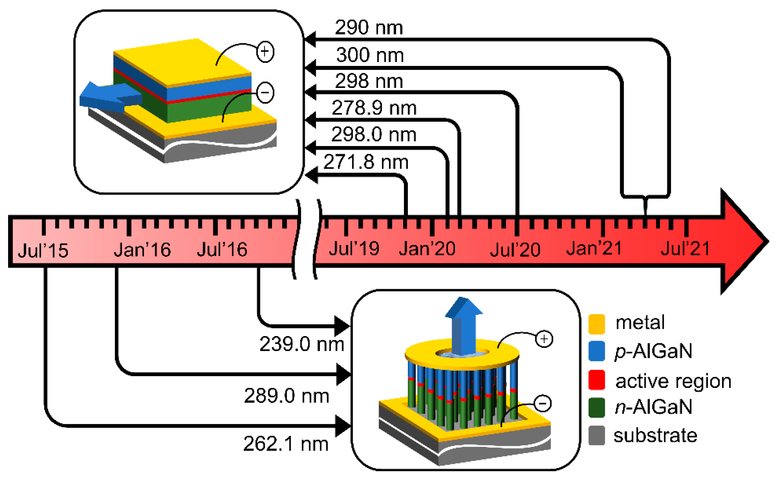
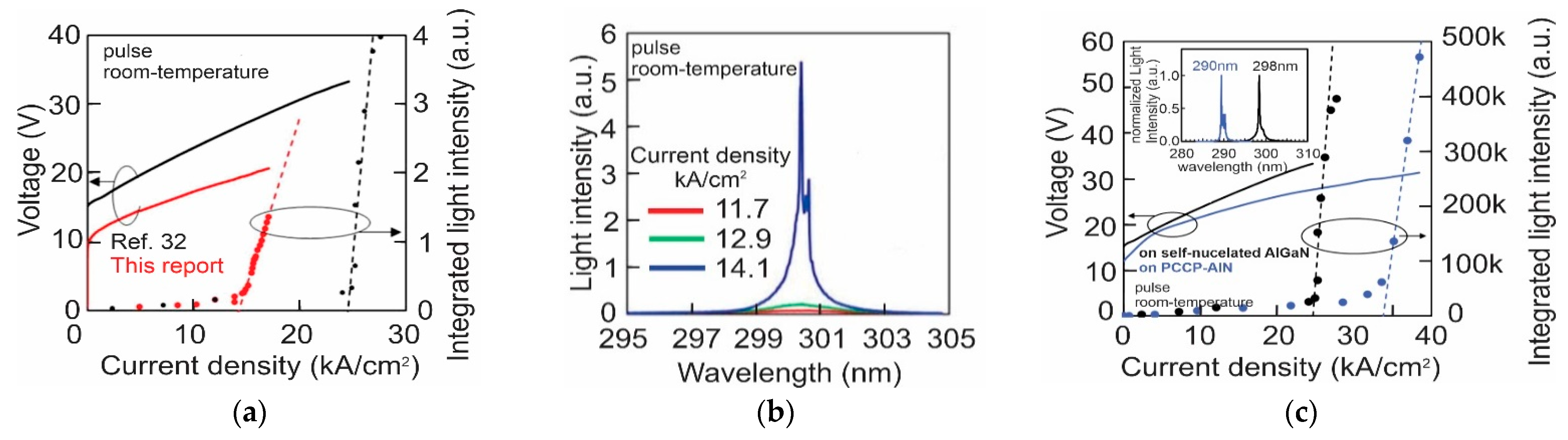
5. Demonstration of AlGaN Lasers
5.1. Thin Film Lasers
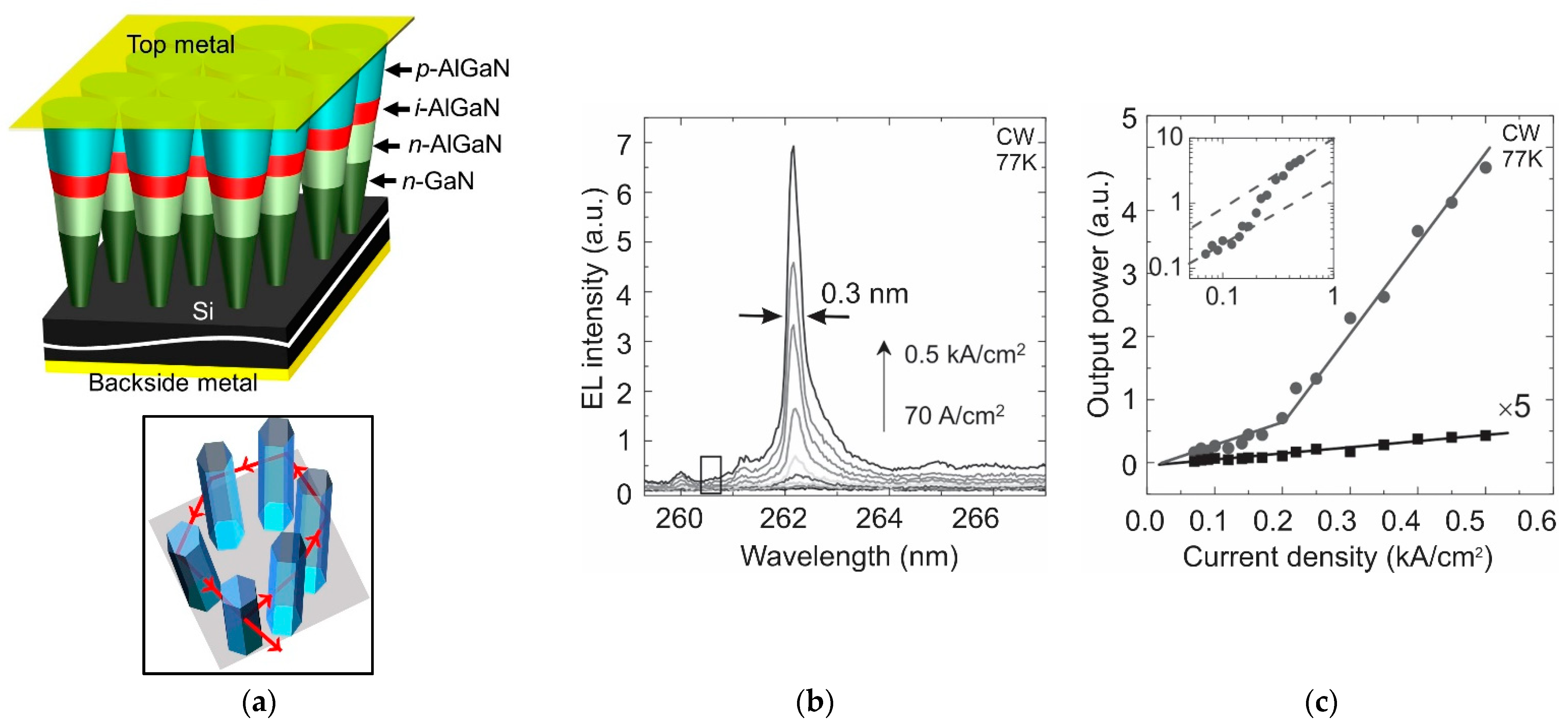
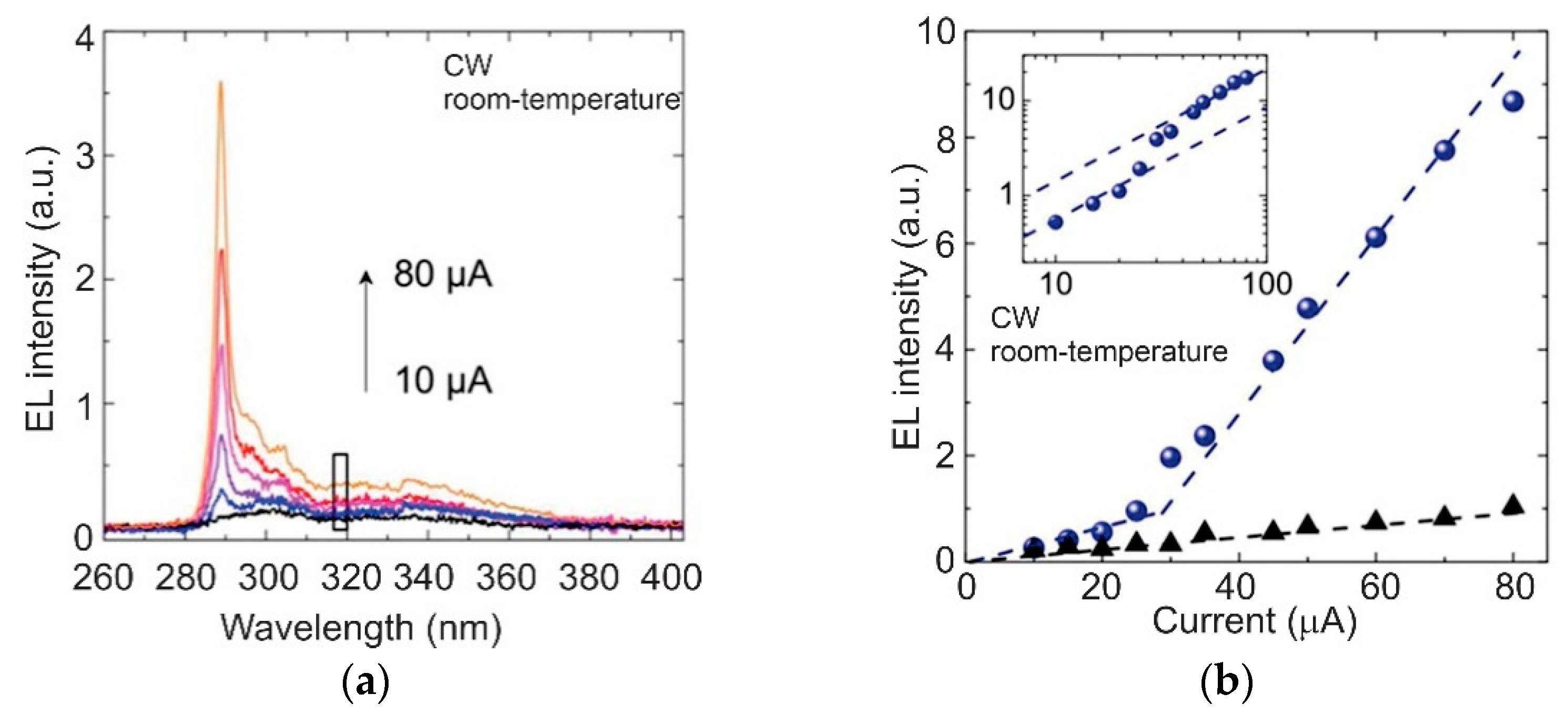
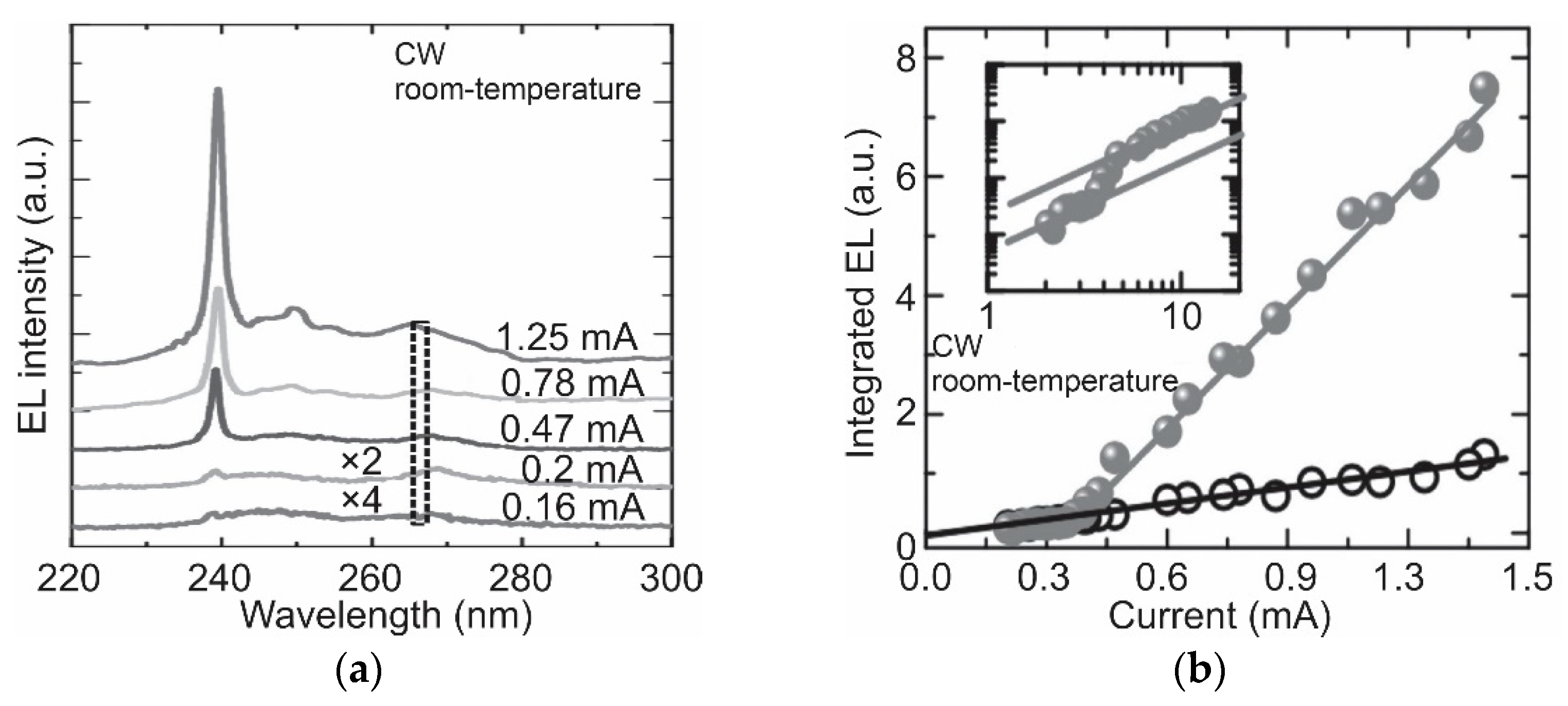
5.2. Nanowire Lasers
6. Conclusions
Author Contributions
Funding
Conflicts of Interest
References
- Majumdar, A.K. Non-line-of-sight (NLOS) ultraviolet and indoor free-space optical (FSO) communications. In Advanced Free Space Optics (FSO); Springer: Berlin/Heidelberg, Germany, 2015; pp. 177–202. [Google Scholar]
- Reilly, D.M.; Moriarty, D.T.; Maynard, J.A. Unique properties of solar blind ultraviolet communication systems for unattended ground sensor networks. In Proceedings of the Unmanned/Unattended Sensors and Sensor Networks, London, UK, 1 September 2004; pp. 244–254. [Google Scholar]
- Bhar, G.; Chatterjee, U. Development of ultraviolet laser for disinfection of potable water. Indian J. Phys. 2006, 80, 517–521. [Google Scholar]
- Vilhunen, S.; Särkkä, H.; Sillanpää, M. Ultraviolet light-emitting diodes in water disinfection. Environ. Sci. Pollut. Res. 2009, 16, 439–442. [Google Scholar] [CrossRef]
- Grishkanich, A.; Zhevlakov, A.; Kascheev, S.; Polyakov, V.; Sidorov, I.; Ruzankina, J.; Yakovlev, A.; Mak, A. Study methods for disinfection water for injection. In Proceedings of the Biophotonics: Photonic Solutions for Better Health Care V, Brussels, Belgium, 4–7 April 2016; p. 98873K. [Google Scholar]
- Nelson, J.S.; Berns, M.W. Laser applications in biomedicine. Part II: Clinical applications. J. Laser Appl. 1989, 1, 9–20. [Google Scholar] [CrossRef]
- Letokhov, V.S. Laser light in biomedicine and the life sciences: From the present to the future. In Biomedical Photonics Handbook; CRC Press: Boca Raton, FL, USA, 2003; pp. 177–192. [Google Scholar]
- Raeiszadeh, M.; Adeli, B. A Critical Review on Ultraviolet Disinfection Systems against COVID-19 Outbreak: Applicability, Validation, and Safety Considerations. ACS Photon. 2020, 7, 2941–2951. [Google Scholar] [CrossRef]
- Gerchman, Y.; Mamane, H.; Friedman, N.; Mandelboim, M. UV-LED disinfection of Coronavirus: Wavelength effect. J. Photochem. Photobiol. B Biol. 2020, 212, 112044. [Google Scholar] [CrossRef]
- Armstrong, A.; Allerman, A.A.; Fischer, A.J.; King, M.P.; Van Heukelom, M.; Moseley, M.W.; Kaplar, R.; Wierer, J.; Crawford, M.H.; Dickerson, J.R. Ultra-Wide Bandgap AlGaN Materials for Electronics and Opto-Electronics; Sandia National Lab. (SNL-NM): Albuquerque, NM, USA, 2016.
- Taniyasu, Y.; Kasu, M.; Makimoto, T. An aluminium nitride light-emitting diode with a wavelength of 210 nanometres. Nature 2006, 441, 325–328. [Google Scholar] [CrossRef]
- Wagner, R.; Levitt, A.P. Whisker Technology; Levitt, A.P., Ed.; Wiley: New York, NY, USA, 1970; pp. 47–119. [Google Scholar]
- Akasaki, I.; Sota, S.; Sakai, H.; Tanaka, T.; Koike, M.; Amano, H. Shortest wavelength semiconductor laser diode. Electron. Lett. 1996, 32, 1105–1106. [Google Scholar] [CrossRef]
- Iida, K.; Kawashima, T.; Miyazaki, A.; Kasugai, H.; Mishima, S.; Honshio, A.; Miyake, Y.; Iwaya, M.; Kamiyama, S.; Amano, H. 350.9 nm UV laser diode grown on low-dislocation-density AlGaN. Jpn. J. Appl. Phys. 2004, 43, L499. [Google Scholar] [CrossRef]
- Masui, S.; Matsuyama, Y.; Yanamoto, T.; Kozaki, T.; Nagahama, S.-I.; Mukai, T. 365 nm ultraviolet laser diodes composed of quaternary AlInGaN alloy. Jpn. J. Appl. Phys. 2003, 42, L1318. [Google Scholar] [CrossRef]
- Kneissl, M.; Treat, D.W.; Teepe, M.; Miyashita, N.; Johnson, N.M. Ultraviolet AlGaN multiple-quantum-well laser diodes. Appl. Phys. Lett. 2003, 82, 4441–4443. [Google Scholar] [CrossRef]
- Kneissl, M.; Yang, Z.; Teepe, M.; Knollenberg, C.; Schmidt, O.; Kiesel, P.; Johnson, N.M.; Schujman, S.; Schowalter, L.J. Ultraviolet semiconductor laser diodes on bulk AlN. J. Appl. Phys. 2007, 101, 123103. [Google Scholar] [CrossRef]
- Yoshida, H.; Yamashita, Y.; Kuwabara, M.; Kan, H. A 342-nm ultraviolet AlGaN multiple-quantum-well laser diode. Nat. Photon. 2008, 2, 551–554. [Google Scholar] [CrossRef]
- Aoki, Y.; Kuwabara, M.; Yamashita, Y.; Takagi, Y.; Sugiyama, A.; Yoshida, H. A 350-nm-band GaN/AlGaN multiple-quantum-well laser diode on bulk GaN. Appl. Phys. Lett. 2015, 107, 151103. [Google Scholar] [CrossRef]
- Wunderer, T.; Chua, C.; Northrup, J.; Yang, Z.; Johnson, N.; Kneissl, M.; Garrett, G.; Shen, H.; Wraback, M.; Moody, B. Optically pumped UV lasers grown on bulk AlN substrates. Phys. Status Solidi C 2012, 9, 822–825. [Google Scholar] [CrossRef]
- Kirste, R.; Guo, Q.; Dycus, J.H.; Franke, A.; Mita, S.; Sarkar, B.; Reddy, P.; LeBeau, J.M.; Collazo, R.; Sitar, Z. 6 kW/cm2 UVC laser threshold in optically pumped lasers achieved by controlling point defect formation. Appl. Phys. Express 2018, 11, 082101. [Google Scholar] [CrossRef]
- Guo, Q.; Kirste, R.; Reddy, P.; Mecouch, W.; Guan, Y.; Mita, S.; Washiyama, S.; Tweedie, J.; Sitar, Z.; Collazo, R. Impact of the effective refractive index in AlGaN-based mid-UV laser structures on waveguiding. Jpn. J. Appl. Phys. 2020, 59, 091001. [Google Scholar] [CrossRef]
- Kawase, Y.; Ikeda, S.; Sakuragi, Y.; Yasue, S.; Iwayama, S.; Iwaya, M.; Takeuchi, T.; Kamiyama, S.; Akasaki, I.; Miyake, H. Ultraviolet-B band lasers fabricated on highly relaxed thick Al0. 55Ga0. 45N films grown on various types of AlN wafers. Jpn. J. Appl. Phys. 2019, 58, SC1052. [Google Scholar] [CrossRef]
- Kuhn, C.; Martens, M.; Mehnke, F.; Enslin, J.; Schneider, P.; Reich, C.; Krueger, F.; Rass, J.; Park, J.B.; Kueller, V. Influence of waveguide strain and surface morphology on AlGaN-based deep UV laser characteristics. J. Phys. D Appl. Phys. 2018, 51, 415101. [Google Scholar] [CrossRef]
- Zhao, S.; Connie, A.; Dastjerdi, M.; Kong, X.; Wang, Q.; Djavid, M.; Sadaf, S.; Liu, X.; Shih, I.; Guo, H. Aluminum nitride nanowire light emitting diodes: Breaking the fundamental bottleneck of deep ultraviolet light sources. Sci. Rep. 2015, 5, 8332. [Google Scholar] [CrossRef]
- Li, K.; Liu, X.; Wang, Q.; Zhao, S.; Mi, Z. Ultralow-threshold electrically injected AlGaN nanowire ultraviolet lasers on Si operating at low temperature. Nat. Nanotechnol. 2015, 10, 140. [Google Scholar] [CrossRef]
- Zhao, S.; Woo, S.; Bugnet, M.; Liu, X.; Kang, J.; Botton, G.; Mi, Z. Three-dimensional quantum confinement of charge carriers in self-organized AlGaN nanowires: A viable route to electrically injected deep ultraviolet lasers. Nano Lett. 2015, 15, 7801–7807. [Google Scholar] [CrossRef] [PubMed]
- Zhao, S.; Liu, X.; Woo, S.; Kang, J.; Botton, G.; Mi, Z. An electrically injected AlGaN nanowire laser operating in the ultraviolet-C band. Appl. Phys. Lett. 2015, 107, 043101. [Google Scholar] [CrossRef]
- Zhao, S.; Liu, X.; Wu, Y.; Mi, Z. An electrically pumped 239 nm AlGaN nanowire laser operating at room temperature. Appl. Phys. Lett. 2016, 109, 191106. [Google Scholar] [CrossRef]
- Zhang, Z.; Kushimoto, M.; Sakai, T.; Sugiyama, N.; Schowalter, L.J.; Sasaoka, C.; Amano, H. A 271.8 nm deep-ultraviolet laser diode for room temperature operation. Appl. Phys. Express 2019, 12, 124003. [Google Scholar] [CrossRef]
- Sato, K.; Yasue, S.; Yamada, K.; Tanaka, S.; Omori, T.; Ishizuka, S.; Teramura, S.; Ogino, Y.; Iwayama, S.; Miyake, H. Room-temperature operation of AlGaN ultraviolet-B laser diode at 298 nm on lattice-relaxed Al0. 6Ga0. 4N/AlN/sapphire. Appl. Phys. Express 2020, 13, 031004. [Google Scholar] [CrossRef] [Green Version]
- Omori, T.; Ishizuka, S.; Tanaka, S.; Yasue, S.; Sato, K.; Ogino, Y.; Teramura, S.; Yamada, K.; Iwayama, S.; Miyake, H. Internal loss of AlGaN-based ultraviolet-B band laser diodes with p-type AlGaN cladding layer using polarization doping. Appl. Phys. Express 2020, 13, 071008. [Google Scholar] [CrossRef]
- Sakai, T.; Kushimoto, M.; Zhang, Z.; Sugiyama, N.; Schowalter, L.J.; Honda, Y.; Sasaoka, C.; Amano, H. On-wafer fabrication of etched-mirror UV-C laser diodes with the ALD-deposited DBR. Appl. Phys. Lett. 2020, 116, 122101. [Google Scholar] [CrossRef] [Green Version]
- Kushimoto, M.; Zhang, Z.; Sugiyama, N.; HONDA, Y.; Schowalter, L.J.; Sasaoka, C.; Amano, H. Impact of heat treatment process on threshold current density in AlGaN-based deep-ultraviolet laser diodes on AlN substrate. Appl. Phys. Express 2021, 14, 051003. [Google Scholar] [CrossRef]
- Tanaka, S.; Ogino, Y.; Yamada, K.; Omori, T.; Ogura, R.; Teramura, S.; Shimokawa, M.; Ishizuka, S.; Yabutani, A.; Iwayama, S. AlGaN-based UV-B laser diode with a high optical confinement factor. Appl. Phys. Lett. 2021, 118, 163504. [Google Scholar] [CrossRef]
- Tanaka, S.; Teramura, S.; Shimokawa, M.; Yamada, K.; Omori, T.; Iwayama, S.; Sato, K.; Miyake, H.; Iwaya, M.; Takeuchi, T. AlGaN-based UV-B laser diode with a wavelength of 290 nm on 1 μm periodic concavo–convex pattern AlN on a sapphire substrate. Appl. Phys. Express 2021, 14, 055505. [Google Scholar] [CrossRef]
- Sato, K.; Omori, T.; Yamada, K.; Tanaka, S.; Ishizuka, S.; Teramura, S.; Iwayama, S.; Iwaya, M.; Miyake, H.; Takeuchi, T. Analysis of carrier injection efficiency of AlGaN UV-B laser diodes based on the relationship between threshold current density and cavity length. Jpn. J. Appl. Phys. 2021, 60, 074002. [Google Scholar] [CrossRef]
- Knelangen, M.; Consonni, V.; Trampert, A.; Riechert, H. In situ analysis of strain relaxation during catalyst-free nucleation and growth of GaN nanowires. Nanotechnology 2010, 21, 245705. [Google Scholar] [CrossRef] [PubMed]
- Chen, Y.; Washburn, J. Structural transition in large-lattice-mismatch heteroepitaxy. Phys. Rev. Lett. 1996, 77, 4046. [Google Scholar] [CrossRef] [PubMed]
- Fang, Z.; Robin, E.; Rozas-Jiménez, E.; Cros, A.; Donatini, F.; Mollard, N.; Pernot, J.; Daudin, B. Si donor incorporation in GaN nanowires. Nano Lett. 2015, 15, 6794–6801. [Google Scholar] [CrossRef] [PubMed]
- Xie, P.; Hu, Y.; Fang, Y.; Huang, J.; Lieber, C.M. Diameter-dependent dopant location in silicon and germanium nanowires. Proc. Natl. Acad. Sci. USA 2009, 106, 15254–15258. [Google Scholar] [CrossRef] [PubMed] [Green Version]
- Mi, Z.; Zhao, S.; Woo, S.; Bugnet, M.; Djavid, M.; Liu, X.; Kang, J.; Kong, X.; Ji, W.; Guo, H. Molecular beam epitaxial growth and characterization of Al (Ga) N nanowire deep ultraviolet light emitting diodes and lasers. J. Phys. D Appl. Phys. 2016, 49, 364006. [Google Scholar] [CrossRef]
- Nagasawa, Y.; Hirano, A. A review of AlGaN-based deep-ultraviolet light-emitting diodes on sapphire. Appl. Sci. 2018, 8, 1264. [Google Scholar] [CrossRef] [Green Version]
- Zhao, S.; Lu, J.; Hai, X.; Yin, X. AlGaN nanowires for ultraviolet light-emitting: Recent progress, challenges, and prospects. Micromachines 2020, 11, 125. [Google Scholar] [CrossRef] [Green Version]
- Zhao, S.; Mi, Z. AlGaN Nanowires: Path to Electrically Injected Semiconductor Deep Ultraviolet Lasers; IEEE: Piscataway, NJ, USA, 2018; Volume 54, pp. 1–9. [Google Scholar]
- Wernicke, T.; Sulmoni, L.; Kuhn, C.; Tränkle, G.; Weyers, M.; Kneissl, M. Group III-Nitride-Based UV Laser Diodes. In Semiconductor Nanophotonics: Materials, Models, and Devices; Kneissl, M., Knorr, A., Reitzenstein, S., Hoffmann, A., Eds.; Springer International Publishing: Cham, Switzerland, 2020; pp. 505–548. [Google Scholar]
- Wunderer, T.; Northrup, J.E.; Johnson, N.M. AlGaN-based ultraviolet laser diodes. III-Nitride Ultrav. Emit. 2016, 193–217. [Google Scholar]
- Li, D.; Jiang, K.; Sun, X.; Guo, C. AlGaN photonics: Recent advances in materials and ultraviolet devices. Adv. Opt. Photon. 2018, 10, 43–110. [Google Scholar] [CrossRef]
- Arafin, S.; Liu, X.; Mi, Z. Review of recent progress of III-nitride nanowire lasers. J. Nanophoton. 2013, 7, 074599. [Google Scholar] [CrossRef]
- Zhang, Q.; Yin, X.; Zhao, S. Recent Progress on Aluminum Gallium Nitride Deep Ultraviolet Lasers by Molecular Beam Epitaxy. Phys. Status Solidi (RRL)–Rapid Res. Lett. 2021, 2100090. [Google Scholar] [CrossRef]
- Electronics, B. UV Light Emitting DIodes (UV A/B/C LEDs). Available online: https://www.boselec.com/product-category/uv-light-emitting-diodes-uv-led (accessed on 7 July 2021).
- Lumileds. LUXEON UV LEDs. Available online: https://www.lumileds.com/products/uv-leds/ (accessed on 7 July 2021).
- Zhang, Z.; Kushimoto, M.; Sakai, T.; Sugiyama, N.; Schowalter, L.J.; Sasaoka, C.; Amano, H. Design and characterization of a low-optical-loss UV-C laser diode. Jpn. J. Appl. Phys. 2020, 59, 094001. [Google Scholar] [CrossRef]
- Guo, Q.; Kirste, R.; Mita, S.; Tweedie, J.; Reddy, P.; Moody, B.; Guan, Y.; Washiyama, S.; Klump, A.; Sitar, Z. Design of AlGaN-based quantum structures for low threshold UVC lasers. J. Appl. Phys. 2019, 126, 223101. [Google Scholar] [CrossRef]
- Zhang, Y.; Krishnamoorthy, S.; Akyol, F.; Allerman, A.A.; Moseley, M.W.; Armstrong, A.M.; Rajan, S. Design of p-type cladding layers for tunnel-injected UV-A light emitting diodes. Appl. Phys. Lett. 2016, 109, 191105. [Google Scholar] [CrossRef] [Green Version]
- Martens, M.; Kuhn, C.; Ziffer, E.; Simoneit, T.; Kueller, V.; Knauer, A.; Rass, J.; Wernicke, T.; Einfeldt, S.; Weyers, M. Low absorption loss p-AlGaN superlattice cladding layer for current-injection deep ultraviolet laser diodes. Appl. Phys. Lett. 2016, 108, 151108. [Google Scholar] [CrossRef]
- Mueller, S.G.; Bondokov, R.T.; Morgan, K.E.; Slack, G.A.; Schujman, S.B.; Grandusky, J.; Smart, J.A.; Schowalter, L.J. The progress of AlN bulk growth and epitaxy for electronic applications. Phys. Status Solidi (A) 2009, 206, 1153–1159. [Google Scholar] [CrossRef]
- Bryan, Z.; Bryan, I.; Xie, J.; Mita, S.; Sitar, Z.; Collazo, R. High internal quantum efficiency in AlGaN multiple quantum wells grown on bulk AlN substrates. Appl. Phys. Lett. 2015, 106, 142107. [Google Scholar] [CrossRef]
- Grandusky, J.R.; Chen, J.; Gibb, S.R.; Mendrick, M.C.; Moe, C.G.; Rodak, L.; Garrett, G.A.; Wraback, M.; Schowalter, L.J. 270 nm pseudomorphic ultraviolet light-emitting diodes with over 60 mW continuous wave output power. Appl. Phys. Express 2013, 6, 032101. [Google Scholar] [CrossRef]
- Yoshida, H.; Yamashita, Y.; Kuwabara, M.; Kan, H. Demonstration of an ultraviolet 336 nm AlGaN multiple-quantum-well laser diode. Appl. Phys. Lett. 2008, 93, 241106. [Google Scholar] [CrossRef]
- Hirayama, H.; Maeda, N.; Fujikawa, S.; Toyoda, S.; Kamata, N. Recent progress and future prospects of AlGaN-based high-efficiency deep-ultraviolet light-emitting diodes. Jpn. J. Appl. Phys. 2014, 53, 100209. [Google Scholar] [CrossRef]
- Shatalov, M.; Sun, W.; Lunev, A.; Hu, X.; Dobrinsky, A.; Bilenko, Y.; Yang, J.; Shur, M.; Gaska, R.; Moe, C. AlGaN deep-ultraviolet light-emitting diodes with external quantum efficiency above 10%. Appl. Phys. Express 2012, 5, 082101. [Google Scholar] [CrossRef]
- Ban, K.; Yamamoto, J.-i.; Takeda, K.; Ide, K.; Iwaya, M.; Takeuchi, T.; Kamiyama, S.; Akasaki, I.; Amano, H. Internal quantum efficiency of whole-composition-range AlGaN multiquantum wells. Appl. Phys. Express 2011, 4, 052101. [Google Scholar] [CrossRef]
- Hirayama, H. Growth of High-Quality AlN on Sapphire and Development of AlGaN-Based Deep-Ultraviolet Light-Emitting Diodes. In Semiconductors and Semimetals; Elsevier: Amsterdam, The Netherlands, 2017; Volume 96, pp. 85–120. [Google Scholar]
- Hwang, S.; Morgan, D.; Kesler, A.; Lachab, M.; Zhang, B.; Heidari, A.; Nazir, H.; Ahmad, I.; Dion, J.; Fareed, Q. 276 nm substrate-free flip-chip AlGaN light-emitting diodes. Appl. Phys. Express 2011, 4, 032102. [Google Scholar] [CrossRef]
- Susilo, N.; Hagedorn, S.; Jaeger, D.; Miyake, H.; Zeimer, U.; Reich, C.; Neuschulz, B.; Sulmoni, L.; Guttmann, M.; Mehnke, F. AlGaN-based deep UV LEDs grown on sputtered and high temperature annealed AlN/sapphire. Appl. Phys. Lett. 2018, 112, 041110. [Google Scholar] [CrossRef]
- Kim, M.; Fujita, T.; Fukahori, S.; Inazu, T.; Pernot, C.; Nagasawa, Y.; Hirano, A.; Ippommatsu, M.; Iwaya, M.; Takeuchi, T. AlGaN-based deep ultraviolet light-emitting diodes fabricated on patterned sapphire substrates. Appl. Phys. Express 2011, 4, 092102. [Google Scholar] [CrossRef]
- Hartmann, C.; Wollweber, J.; Sintonen, S.; Dittmar, A.; Kirste, L.; Kollowa, S.; Irmscher, K.; Bickermann, M. Preparation of deep UV transparent AlN substrates with high structural perfection for optoelectronic devices. Cryst. Eng. Comm. 2016, 18, 3488–3497. [Google Scholar] [CrossRef]
- Li, J.; Oder, T.; Nakarmi, M.; Lin, J.; Jiang, H. Optical and electrical properties of Mg-doped p-type AlxGa1−xN. Appl. Phys. Lett. 2002, 80, 1210–1212. [Google Scholar] [CrossRef]
- Suzuki, M.; Nishio, J.; Onomura, M.; Hongo, C. Doping characteristics and electrical properties of Mg-doped AlGaN grown by atmospheric-pressure MOCVD. J. Cryst. Growth 1998, 189, 511–515. [Google Scholar] [CrossRef]
- Jeon, S.-R.; Ren, Z.; Cui, G.; Su, J.; Gherasimova, M.; Han, J.; Cho, H.-K.; Zhou, L. Investigation of Mg doping in high-Al content p-type AlxGa1−xN (0.3 < x < 0.5). Appl. Phys. Lett. 2005, 86, 082107. [Google Scholar]
- Kinoshita, T.; Obata, T.; Yanagi, H.; Inoue, S.-i. High p-type conduction in high-Al content Mg-doped AlGaN. Appl. Phys. Lett. 2013, 102, 012105. [Google Scholar] [CrossRef]
- Borisov, B.; Kuryatkov, V.; Kudryavtsev, Y.; Asomoza, R.; Nikishin, S.; Song, D.; Holtz, M.; Temkin, H. Si-doped AlxGa1−xN (0.56 ≤ x ≤ 1) layers grown by molecular beam epitaxy with ammonia. Appl. Phys. Lett. 2005, 87, 132106. [Google Scholar] [CrossRef] [Green Version]
- Mehnke, F.; Wernicke, T.; Pingel, H.; Kuhn, C.; Reich, C.; Kueller, V.; Knauer, A.; Lapeyrade, M.; Weyers, M.; Kneissl, M. Highly conductive n-Al x Ga1− x N layers with aluminum mole fractions above 80%. Appl. Phys. Lett. 2013, 103, 212109. [Google Scholar] [CrossRef]
- Taniyasu, Y.; Kasu, M.; Kobayashi, N. Intentional control of n-type conduction for Si-doped AlN and AlxGa1−xN (0.42 ≤ x < 1). Appl. Phys. Lett. 2002, 81, 1255–1257. [Google Scholar]
- Katsuragawa, M.; Sota, S.; Komori, M.; Anbe, C.; Takeuchi, T.; Sakai, H.; Amano, H.; Akasaki, I. Thermal ionization energy of Si and Mg in AlGaN. J. Cryst. Growth 1998, 189, 528–531. [Google Scholar] [CrossRef]
- Epelbaum, B.M.; Bickermann, M.; Winnacker, A. Seeded PVT growth of aluminum nitride on silicon carbide. In Materials Science Forum; Trans Tech Publications Ltd.: Schwyz, Switzerland, 2003; pp. 983–986. [Google Scholar]
- Bickermann, M.; Epelbaum, B.M.; Filip, O.; Heimann, P.; Nagata, S.; Winnacker, A. UV transparent single-crystalline bulk AlN substrates. Phys. Status Solidi C 2010, 7, 21–24. [Google Scholar] [CrossRef]
- HexaTech, Inc. HexaTech Demonstrates 2-Inch Aluminum Nitride Substrate with Absorption of 12 cm−1 at 265 nm; HexaTech, Inc.: Morrisville, NC, USA, 2021. [Google Scholar]
- Dalmau, R.; Moody, B.; Schlesser, R.; Mita, S.; Xie, J.; Feneberg, M.; Neuschl, B.; Thonke, K.; Collazo, R.; Rice, A. Growth and characterization of AlN and AlGaN epitaxial films on AlN single crystal substrates. J. Electrochem. Soc. 2011, 158, H530. [Google Scholar] [CrossRef]
- Grandusky, J.R.; Gibb, S.R.; Mendrick, M.C.; Schowalter, L.J. Properties of mid-ultraviolet light emitting diodes fabricated from pseudomorphic layers on bulk aluminum nitride substrates. Appl. Phys. Express 2010, 3, 072103. [Google Scholar] [CrossRef]
- Bryan, I.; Bryan, Z.; Washiyama, S.; Reddy, P.; Gaddy, B.; Sarkar, B.; Breckenridge, M.H.; Guo, Q.; Bobea, M.; Tweedie, J. Doping and compensation in Al-rich AlGaN grown on single crystal AlN and sapphire by MOCVD. Appl. Phys. Lett. 2018, 112, 062102. [Google Scholar] [CrossRef]
- Schulz, T.; Irmscher, K.; Albrecht, M.; Hartmann, C.; Wollweber, J.; Fornari, R. n-type conductivity in sublimation-grown AlN bulk crystals. Phys. Status Solidi (RRL) Rapid Res. Lett. 2007, 1, 147–149. [Google Scholar] [CrossRef]
- Alden, D.; Harris, J.; Bryan, Z.; Baker, J.; Reddy, P.; Mita, S.; Callsen, G.; Hoffmann, A.; Irving, D.; Collazo, R. Point-defect nature of the ultraviolet absorption band in AlN. Phys. Rev. Appl. 2018, 9, 054036. [Google Scholar] [CrossRef] [Green Version]
- Ponce, F.; Major, J., Jr.; Plano, W.; Welch, D. Crystalline structure of AlGaN epitaxy on sapphire using AlN buffer layers. Appl. Phys. Lett. 1994, 65, 2302–2304. [Google Scholar] [CrossRef]
- Nam, K.; Nakarmi, M.; Li, J.; Lin, J.; Jiang, H. Mg acceptor level in AlN probed by deep ultraviolet photoluminescence. Appl. Phys. Lett. 2003, 83, 878–880. [Google Scholar] [CrossRef]
- Abeles, B. Lattice Thermal Conductivity of Disordered Semiconductor Alloys at High Temperatures. Phys. Rev. 1963, 131, 1906–1911. [Google Scholar] [CrossRef]
- Van de Walle, C.G.; Stampfl, C.; Neugebauer, J.; McCluskey, M.; Johnson, N. Doping of aigan alloys. MRS Online Proc. Libr. (OPL) 1998, 537. [Google Scholar] [CrossRef]
- Chakraborty, A.; Moe, C.G.; Wu, Y.; Mates, T.; Keller, S.; Speck, J.S.; DenBaars, S.P.; Mishra, U.K. Electrical and structural characterization of Mg-doped p-type Al 0.69 Ga 0.31 N films on SiC substrate. J. Appl. Phys. 2007, 101, 053717. [Google Scholar] [CrossRef]
- Zvanut, M.; Sunay, U.R.; Dashdorj, J.; Willoughby, W.; Allerman, A. Mg-hydrogen interaction in AlGaN alloys. In Gallium Nitride Materials and Devices VII; International Society for Optics and Photonics: Bellingham, WA, USA, 2012; p. 82620L. [Google Scholar]
- Lyons, J.; Janotti, A.; Van de Walle, C. Effects of carbon on the electrical and optical properties of InN, GaN, and AlN. Phys. Rev. B 2014, 89, 035204. [Google Scholar] [CrossRef]
- Reshchikov, M.A.; Morkoç, H. Luminescence properties of defects in GaN. J. Appl. Phys. 2005, 97, 5–19. [Google Scholar] [CrossRef]
- Gordon, L.; Lyons, J.; Janotti, A.; Van de Walle, C. Hybrid functional calculations of D X centers in AlN and GaN. Phys. Rev. B 2014, 89, 085204. [Google Scholar] [CrossRef]
- Miller, M.; Koo, B.; Bogart, K.; Mohney, S.E. Ti/Al/Ti/Au and V/Al/V/Au Contacts to Plasma-Etched n-Al0.58Ga0.42N. J. Electron. Mater. 2008, 37, 564–568. [Google Scholar] [CrossRef]
- Nagata, N.; Senga, T.; Iwaya, M.; Takeuchi, T.; Kamiyama, S.; Akasaki, I. Reduction of contact resistance in V-based electrode for high AlN molar fraction n-type AlGaN by using thin SiNx intermediate layer. Phys. Status Solidi C 2017, 14, 1600243. [Google Scholar]
- Kaneda, M.; Pernot, C.; Nagasawa, Y.; Hirano, A.; Ippommatsu, M.; Honda, Y.; Amano, H.; Akasaki, I. Uneven AlGaN multiple quantum well for deep-ultraviolet LEDs grown on macrosteps and impact on electroluminescence spectral output. Jpn. J. Appl. Phys. 2017, 56, 061002. [Google Scholar] [CrossRef]
- Takano, T.; Mino, T.; Sakai, J.; Noguchi, N.; Tsubaki, K.; Hirayama, H. Deep-ultraviolet light-emitting diodes with external quantum efficiency higher than 20% at 275 nm achieved by improving light-extraction efficiency. Appl. Phys. Express 2017, 10, 031002. [Google Scholar] [CrossRef]
- Ni, R.; Chuo, C.-C.; Yang, K.; Ai, Y.; Zhang, L.; Cheng, Z.; Liu, Z.; Jia, L.; Zhang, Y. AlGaN-based ultraviolet light-emitting diode on high-temperature annealed sputtered AlN template. J. Alloys Compd. 2019, 794, 8–12. [Google Scholar] [CrossRef]
- Hsu, Y.; Chang, S.-J.; Su, Y.-K.; Sheu, J.-K.; Lee, C.; Wen, T.-C.; Wu, L.; Kuo, C.-H.; Chang, C.; Shei, S.-C. Lateral epitaxial patterned sapphire InGaN/GaN MQW LEDs. J. Cryst. Growth 2004, 261, 466–470. [Google Scholar] [CrossRef]
- Arafin, S.; Hasan, S.M.N.; Jamal-Eddine, Z.; Wickramaratne, D.; Paul, B.; Rajan, S. Design of AlGaN-based lasers with a buried tunnel junction for sub-300 nm emission. Semicond. Sci. Technol. 2019, 34, 074002. [Google Scholar] [CrossRef] [Green Version]
- Arefin, R.; You, W.; Ramachandra, S.H.; Hasan, S.M.; Jung, H.; Awwad, M.; Arafin, S. Theoretical Analysis of Tunnel-Injected Sub-300 nm AlGaN Laser Diodes. IEEE J. Quant. Electron. 2020, 56, 1–10. [Google Scholar]
- Li, X.-H.; Detchprohm, T.; Kao, T.-T.; Satter, M.M.; Shen, S.-C.; Douglas Yoder, P.; Dupuis, R.D.; Wang, S.; Wei, Y.O.; Xie, H. Low-threshold stimulated emission at 249 nm and 256 nm from AlGaN-based multiple-quantum-well lasers grown on sapphire substrates. Appl. Phys. Lett. 2014, 105, 141106. [Google Scholar] [CrossRef]
- Satter, M.M.; Lochner, Z.; Ryou, J.-H.; Shen, S.-C.; Dupuis, R.D.; Yoder, P.D. Polarization matching in AlGaN-based multiple-quantum-well deep ultraviolet laser diodes on AlN substrates using quaternary AlInGaN barriers. J. Lightw. Technol. 2012, 30, 3017–3025. [Google Scholar] [CrossRef]
- Paliwal, A.; Singh, K.; Mathew, M. Effects of AlInN graded polarization-dependent doped top cladding on the performance of deep ultra-violet laser diode emitting at ~271 nm wavelength. Semicond. Sci. Technol. 2020, 36, 015006. [Google Scholar] [CrossRef]
- Guo, Q.; Kirste, R.; Mita, S.; Tweedie, J.; Reddy, P.; Washiyama, S.; Breckenridge, M.H.; Collazo, R.; Sitar, Z. The polarization field in Al-rich AlGaN multiple quantum wells. Jpn. J. Appl. Phys. 2019, 58, SCCC10. [Google Scholar] [CrossRef]
- Liu, L.; Edgar, J.H. Transport effects in the sublimation growth of aluminum nitride. J. Cryst. Growth 2000, 220, 243–253. [Google Scholar] [CrossRef]
- Krukowski, S.; Grzegory, I.; Bockowski, M.; Lucznik, B.; Suski, T.; Nowak, G.; Borysiuk, J.; Wroblewski, M.; Leszczynski, M.; Perlin, P. Growth of AlN, GaN and InN from the solution. Int. J. Mater. Prod. Technol. 2005, 22, 226–261. [Google Scholar] [CrossRef]
- Grzegory, I.; Jun, J.; Boćkowski, M.; Wroblewski, M.; Łucznik, B.; Porowski, S. III–V Nitrides—thermodynamics and crystal growth at high N2 pressure. J. Phys. Chem. Solids 1995, 56, 639–647. [Google Scholar] [CrossRef]
- Zhou, T.; Raghothamachar, B.; Wu, F.; Dalmau, R.; Moody, B.; Craft, S.; Schlesser, R.; Dudley, M.; Sitar, Z. Characterization of threading dislocations in PVT-grown AlN substrates via X-ray topography and ray tracing simulation. J. Electron. Mater. 2014, 43, 838–842. [Google Scholar] [CrossRef]
- Bondokov, R.T.; Mueller, S.G.; Morgan, K.E.; Slack, G.A.; Schujman, S.; Wood, M.C.; Smart, J.A.; Schowalter, L.J. Large-area AlN substrates for electronic applications: An industrial perspective. J. Cryst. Growth 2008, 310, 4020–4026. [Google Scholar] [CrossRef]
- Kinoshita, T.; Obata, T.; Nagashima, T.; Yanagi, H.; Moody, B.; Mita, S.; Inoue, S.-i.; Kumagai, Y.; Koukitu, A.; Sitar, Z. Performance and reliability of deep-ultraviolet light-emitting diodes fabricated on AlN substrates prepared by hydride vapor phase epitaxy. Appl. Phys. Express 2013, 6, 092103. [Google Scholar] [CrossRef]
- Inoue, S.-I.; Naoki, T.; Kinoshita, T.; Obata, T.; Yanagi, H. Light extraction enhancement of 265 nm deep-ultraviolet light-emitting diodes with over 90 mW output power via an AlN hybrid nanostructure. Appl. Phys. Lett. 2015, 106, 131104. [Google Scholar] [CrossRef]
- Martens, M.; Mehnke, F.; Kuhn, C.; Reich, C.; Kueller, V.; Knauer, A.; Netzel, C.; Hartmann, C.; Wollweber, J.; Rass, J. Performance characteristics of UV-C AlGaN-based lasers grown on sapphire and bulk AlN substrates. IEEE Photon. Technol. Lett. 2013, 26, 342–345. [Google Scholar] [CrossRef]
- Bryan, I.; Bryan, Z.; Mita, S.; Rice, A.; Hussey, L.; Shelton, C.; Tweedie, J.; Maria, J.-P.; Collazo, R.; Sitar, Z. The role of surface kinetics on composition and quality of AlGaN. J. Cryst. Growth 2016, 451, 65–71. [Google Scholar] [CrossRef] [Green Version]
- Hexatech Inc. AlN Substrate Products. Available online: https://www.hexatechinc.com/aln-wafer-sales.html (accessed on 7 July 2021).
- MTI Corporation. AlN Single Crystal Substrate <0001>. Available online: https://www.mtixtl.com/AlN-0001-1010045S2.aspx (accessed on 7 July 2021).
- Kymatech Technologies. PVDNC™ AlN Templates. Available online: https://www.kymatech.com/products-services/materials/gan-related-iii-n-materials/498-pvdnc-aln-templates (accessed on 7 July 2021).
- MSE Supplies. Aluminum Nitride AlN Template on Sapphire. Available online: https://www.msesupplies.com/products/2-inch-aluminum-nitride-aln-template-on-sapphire-0001-aln?variant=23763293569082 (accessed on 7 July 2021).
- MTI Corporation. AlN Template on Sapphire. Available online: https://www.mtixtl.com/AlN-on-Al2O3-4.aspx (accessed on 7 July 2021).
- Amano, H.; Collazo, R.; De Santi, C.; Einfeldt, S.; Funato, M.; Glaab, J.; Hagedorn, S.; Hirano, A.; Hirayama, H.; Ishii, R. The 2020 UV emitter roadmap. J. Phys. D Appl. Phys. 2020, 53, 503001. [Google Scholar] [CrossRef]
- Walde, S.; Hagedorn, S.; Weyers, M. Impact of intermediate high temperature annealing on the properties of AlN/sapphire templates grown by metalorganic vapor phase epitaxy. Jpn. J. Appl. Phys. 2019, 58, SC1002. [Google Scholar] [CrossRef]
- Miyake, H.; Nishio, G.; Suzuki, S.; Hiramatsu, K.; Fukuyama, H.; Kaur, J.; Kuwano, N. Annealing of an AlN buffer layer in N2–CO for growth of a high-quality AlN film on sapphire. Appl. Phys. Express 2016, 9, 025501. [Google Scholar] [CrossRef] [Green Version]
- Fukuyama, H.; Miyake, H.; Nishio, G.; Suzuki, S.; Hiramatsu, K. Impact of high-temperature annealing of AlN layer on sapphire and its thermodynamic principle. Jpn. J. Appl. Phys. 2016, 55, 05FL02. [Google Scholar] [CrossRef]
- Miyake, H.; Lin, C.-H.; Tokoro, K.; Hiramatsu, K. Preparation of high-quality AlN on sapphire by high-temperature face-to-face annealing. J. Cryst. Growth 2016, 456, 155–159. [Google Scholar] [CrossRef] [Green Version]
- Kaiser, S.; Jakob, M.; Zweck, J.; Gebhardt, W.; Ambacher, O.; Dimitrov, R.; Schremer, A.; Smart, J.; Shealy, J. Structural properties of AlGaN/GaN heterostructures on Si (111) substrates suitable for high-electron mobility transistors. J. Vac. Sci. Technol. B Microelectron. Nanometer Struct. Process. Meas. Phenom. 2000, 18, 733–740. [Google Scholar] [CrossRef]
- Ishikawa, H.; Zhao, G.-Y.; Nakada, N.; Egawa, T.; Jimbo, T.; Umeno, M. GaN on Si substrate with AlGaN/AlN intermediate layer. Jpn. J. Appl. Phys. 1999, 38, L492. [Google Scholar] [CrossRef]
- Radtke, G.; Couillard, M.; Botton, G.; Zhu, D.; Humphreys, C. Structure and chemistry of the Si (111)/AlN interface. Appl. Phys. Lett. 2012, 100, 011910. [Google Scholar] [CrossRef]
- Bertness, K.A.; Roshko, A.; Sanford, N.A.; Barker, J.; Davydov, A. Spontaneously grown GaN and AlGaN nanowires. J. Cryst. Growth 2006, 287, 522–527. [Google Scholar] [CrossRef]
- Wang, Y.; Dheeraj, D.; Liu, Z.; Liang, M.; Li, Y.; Yi, X.; Wang, J.; Li, J.; Weman, H. AlGaN nanowires grown on SiO2/Si (100) using graphene as a buffer layer. Cryst. Growth Des. 2019, 19, 5516–5522. [Google Scholar] [CrossRef]
- Wu, Y.; Wang, Y.; Sun, K.; Mi, Z. Molecular beam epitaxy and characterization of AlGaN nanowire ultraviolet light emitting diodes on Al coated Si (0 0 1) substrate. J. Cryst. Growth 2019, 507, 65–69. [Google Scholar] [CrossRef]
- Calleja, E.; Sánchez-García, M.; Sanchez, F.; Calle, F.; Naranjo, F.; Munoz, E.; Molina, S.; Sanchez, A.; Pacheco, F.; Garcıa, R. Growth of III-nitrides on Si (1 1 1) by molecular beam epitaxy Doping, optical, and electrical properties. J. Cryst. Growth 1999, 201, 296–317. [Google Scholar] [CrossRef]
- Songmuang, R.; Ben, T.; Daudin, B.; González, D.; Monroy, E. Identification of III–N nanowire growth kinetics via a marker technique. Nanotechnology 2010, 21, 295605. [Google Scholar] [CrossRef]
- Wang, Q.; Zhao, S.; Connie, A.; Shih, I.; Mi, Z.; Gonzalez, T.; Andrews, M.; Du, X.; Lin, J.; Jiang, H. Optical properties of strain-free AlN nanowires grown by molecular beam epitaxy on Si substrates. Appl. Phys. Lett. 2014, 104, 223107. [Google Scholar] [CrossRef] [Green Version]
- Holmes, M.J.; Choi, K.; Kako, S.; Arita, M.; Arakawa, Y. Room-temperature triggered single photon emission from a III-nitride site-controlled nanowire quantum dot. Nano Lett. 2014, 14, 982–986. [Google Scholar] [CrossRef] [PubMed]
- Ra, Y.H.; Kang, S.; Lee, C.R. Ultraviolet Light-Emitting Diode Using Nonpolar AlGaN Core–Shell Nanowire Heterostructures. Adv. Opt. Mater. 2018, 6, 1701391. [Google Scholar] [CrossRef]
- Su, J.; Gherasimova, M.; Cui, G.; Tsukamoto, H.; Han, J.; Onuma, T.; Kurimoto, M.; Chichibu, S.; Broadbridge, C.; He, Y. Growth of AlGaN nanowires by metalorganic chemical vapor deposition. Appl. Phys. Lett. 2005, 87, 183108. [Google Scholar] [CrossRef]
- Godejohann, B.J.; Ture, E.; Müller, S.; Prescher, M.; Kirste, L.; Aidam, R.; Polyakov, V.; Brückner, P.; Breuer, S.; Köhler, K. AlN/GaN HEMTs grown by MBE and MOCVD: Impact of Al distribution. Phys. Status Solidi (B) 2017, 254, 1600715. [Google Scholar] [CrossRef]
- Cordier, Y.; Comyn, R.; Frayssinet, E.; Khoury, M.; Lesecq, M.; Defrance, N.; De Jaeger, J.C. Influence of AlN growth temperature on the electrical properties of buffer layers for GaN HEMTs on silicon. Phys. Status Solidi (A) 2018, 215, 1700637. [Google Scholar] [CrossRef]
- Yang, M.; Wang, W.; Lin, Y.; Yang, W.; Li, G. Epitaxial growth of high quality AlN films on Si substrates. Mater. Lett. 2016, 182, 277–280. [Google Scholar] [CrossRef]
- Ichikawa, M.; Fujioka, A.; Kosugi, T.; Endo, S.; Sagawa, H.; Tamaki, H.; Mukai, T.; Uomoto, M.; Shimatsu, T. High-output-power deep ultraviolet light-emitting diode assembly using direct bonding. Appl. Phys. Express 2016, 9, 072101. [Google Scholar] [CrossRef]
- Wang, T.-Y.; Tasi, C.-T.; Lin, C.-F.; Wuu, D.-S. 85% internal quantum efficiency of 280-nm AlGaN multiple quantum wells by defect engineering. Sci. Rep. 2017, 7, 14422. [Google Scholar] [CrossRef] [PubMed] [Green Version]
- Wunderer, T.; Chua, C.L.; Yang, Z.; Northrup, J.E.; Johnson, N.M.; Garrett, G.A.; Shen, H.; Wraback, M. Pseudomorphically grown ultraviolet C photopumped lasers on bulk AlN substrates. Appl. Phys. Express 2011, 4, 092101. [Google Scholar] [CrossRef]
- Xing, H.; Green, D.S.; Yu, H.; Mates, T.; Kozodoy, P.; Keller, S.; DenBaars, S.P.; Mishra, U.K. Memory effect and redistribution of Mg into sequentially regrown GaN layer by metalorganic chemical vapor deposition. Jpn. J. Appl. Phys. 2003, 42, 50. [Google Scholar] [CrossRef]
- Ivanov, S.; Nechaev, D.; Sitnikova, A.; Ratnikov, V.; Yagovkina, M.; Rzheutskii, N.; Lutsenko, E.; Jmerik, V. Plasma-assisted molecular beam epitaxy of Al (Ga) N layers and quantum well structures for optically pumped mid-UV lasers on c-Al2O3. Semicond. Sci. Technol. 2014, 29, 084008. [Google Scholar] [CrossRef]
- Jmerik, V.; Lutsenko, E.; Ivanov, S. Plasma-assisted molecular beam epitaxy of AlGaN heterostructures for deep-ultraviolet optically pumped lasers. Phys. Status Solidi (A) 2013, 210, 439–450. [Google Scholar] [CrossRef]
- Yang, W.; Zhao, Y.; Wu, Y.; Li, X.; Xing, Z.; Bian, L.; Lu, S.; Luo, M. Deep-UV emission at 260 nm from MBE-grown AlGaN/AlN quantum-well structures. J. Cryst. Growth 2019, 512, 213–218. [Google Scholar] [CrossRef]
- Chang, S.-J.; Lin, W.-H.; Chen, W.-S. Cascaded GaN Light-Emitting Diodes with Hybrid Tunnel Junction Layers; Institute of Electrical and Electronics Engineers: Piscataway, NJ, USA, 2015; Volume 51, pp. 1–5. [Google Scholar]
- Young, E.C.; Yonkee, B.P.; Wu, F.; Oh, S.H.; DenBaars, S.P.; Nakamura, S.; Speck, J.S. Hybrid tunnel junction contacts to III–nitride light-emitting diodes. Appl. Phys. Express 2016, 9, 022102. [Google Scholar] [CrossRef]
- Neugebauer, S.; Hoffmann, M.; Witte, H.; Bläsing, J.; Dadgar, A.; Strittmatter, A.; Niermann, T.; Narodovitch, M.; Lehmann, M. All metalorganic chemical vapor phase epitaxy of p/n-GaN tunnel junction for blue light emitting diode applications. Appl. Phys. Lett. 2017, 110, 102104. [Google Scholar] [CrossRef]
- Wang, J.; Young, E.; SaifAddin, B.; Zollner, C.; Almogbel, A.; Fireman, M.; Izza, M.; Nakamura, S.; Denbaars, S.; Speck, J. Hybrid III-Nitride Tunnel Junctions for Low Excess Voltage Blue LEDs and UVC LEDs. In Proceedings of the 2019 Compound Semiconductor Week (CSW), Nara, Japan, 19–23 May 2019; p. 1. [Google Scholar]
- Clinton, E.A.; Vadiee, E.; Shen, S.-C.; Mehta, K.; Yoder, P.D.; Doolittle, W.A. Negative differential resistance in GaN homojunction tunnel diodes and low voltage loss tunnel contacts. Appl. Phys. Lett. 2018, 112, 252103. [Google Scholar] [CrossRef]
- Shatalov, M.; Jain, R.; Saxena, T.; Dobrinsky, A.; Shur, M. Development of deep UV LEDs and current problems in material and device technology. In Semiconductors and Semimetals; Elsevier: Amsterdam, The Netherlands, 2017; Volume 96, pp. 45–83. [Google Scholar]
- Jena, D.; Heikman, S.; Green, D.; Buttari, D.; Coffie, R.; Xing, H.; Keller, S.; DenBaars, S.; Speck, J.S.; Mishra, U.K. Realization of wide electron slabs by polarization bulk doping in graded III–V nitride semiconductor alloys. Appl. Phys. Lett. 2002, 81, 4395–4397. [Google Scholar] [CrossRef] [Green Version]
- Zhang, Z.; Kushimoto, M.; Horita, M.; Sugiyama, N.; Schowalter, L.J.; Sasaoka, C.; Amano, H. Space charge profile study of AlGaN-based p-type distributed polarization doped claddings without impurity doping for UV-C laser diodes. Appl. Phys. Lett. 2020, 117, 152104. [Google Scholar] [CrossRef]
- Chang, J.; Chen, D.; Xue, J.; Dong, K.; Liu, B.; Lu, H.; Zhang, R.; Zheng, Y. AlGaN-Based Multiple Quantum Well Deep Ultraviolet Light-Emitting Diodes with Polarization Doping; Institute of Electrical and Electronics Engineers: Piscataway, NJ, USA, 2016; Volume 8, pp. 1–7. [Google Scholar]
- Yasuda, T.; Takeuchi, T.; Iwaya, M.; Kamiyama, S.; Akasaki, I.; Amano, H. Relationship between lattice relaxation and electrical properties in polarization doping of graded AlGaN with high AlN mole fraction on AlGaN template. Appl. Phys. Express 2017, 10, 025502. [Google Scholar] [CrossRef]
- Simon, J.; Protasenko, V.; Lian, C.; Xing, H.; Jena, D. Polarization-induced hole doping in wide–band-gap uniaxial semiconductor heterostructures. Science 2010, 327, 60–64. [Google Scholar] [CrossRef] [PubMed] [Green Version]
- Cheng, B.; Choi, S.; Northrup, J.; Yang, Z.; Knollenberg, C.; Teepe, M.; Wunderer, T.; Chua, C.; Johnson, N. Enhanced vertical and lateral hole transport in high aluminum-containing AlGaN for deep ultraviolet light emitters. Appl. Phys. Lett. 2013, 102, 231106. [Google Scholar] [CrossRef]
- Zheng, T.; Lin, W.; Liu, R.; Cai, D.; Li, J.; Li, S.; Kang, J. Improved p-type conductivity in Al-rich AlGaN using multidimensional Mg-doped superlattices. Sci. Rep. 2016, 6, 21897. [Google Scholar] [CrossRef] [PubMed] [Green Version]
- Ebata, K.; Nishinaka, J.; Taniyasu, Y.; Kumakura, K. High hole concentration in Mg-doped AlN/AlGaN superlattices with high Al content. Jpn. J. Appl. Phys. 2018, 57, 04FH09. [Google Scholar] [CrossRef]
- Si, Q.; Chen, H.; Li, S.; Lu, S.; Kang, J. Improved characteristics of AlGaN-Based Deep Ultraviolet Light-Emitting Diodes with Superlattice P-Type Doping; Institute of Electrical and Electronics Engineers: Piscataway, NJ, USA, 2017; Volume 9, pp. 1–7. [Google Scholar]
- Takeuchi, T.; Hasnain, G.; Corzine, S.; Hueschen, M.; Schneider, R.P., Jr.; Kocot, C.; Blomqvist, M.; Chang, Y.-L.; Lefforge, D.; Krames, M.R. GaN-based light emitting diodes with tunnel junctions. Jpn. J. Appl. Phys. 2001, 40, L861. [Google Scholar] [CrossRef]
- Zhang, Y.; Krishnamoorthy, S.; Akyol, F.; Allerman, A.A.; Moseley, M.W.; Armstrong, A.M.; Rajan, S. Design and demonstration of ultra-wide bandgap AlGaN tunnel junctions. Appl. Phys. Lett. 2016, 109, 121102. [Google Scholar] [CrossRef]
- Krishnamoorthy, S.; Akyol, F.; Park, P.S.; Rajan, S. Low resistance GaN/InGaN/GaN tunnel junctions. Appl. Phys. Lett. 2013, 102, 113503. [Google Scholar] [CrossRef]
- Zhang, Y.; Jamal-Eddine, Z.; Akyol, F.; Bajaj, S.; Johnson, J.M.; Calderon, G.; Allerman, A.A.; Moseley, M.W.; Armstrong, A.M.; Hwang, J. Tunnel-injected sub 290 nm ultra-violet light emitting diodes with 2.8% external quantum efficiency. Appl. Phys. Lett. 2018, 112, 071107. [Google Scholar] [CrossRef]
- Zhao, S.; Sadaf, S.; Vanka, S.; Wang, Y.; Rashid, R.; Mi, Z. Sub-milliwatt AlGaN nanowire tunnel junction deep ultraviolet light emitting diodes on silicon operating at 242 nm. Appl. Phys. Lett. 2016, 109, 201106. [Google Scholar] [CrossRef]
- Lee, S.-N.; Cho, S.; Ryu, H.; Son, J.; Paek, H.; Sakong, T.; Jang, T.; Choi, K.; Ha, K.; Yang, M. High-power GaN-based blue-violet laser diodes with AlGaN∕ GaN multiquantum barriers. Appl. Phys. Lett. 2006, 88, 111101. [Google Scholar] [CrossRef]
- Chen, J.-R.; Ko, T.-S.; Su, P.-Y.; Lu, T.-C.; Kuo, H.-C.; Kuo, Y.-K.; Wang, S.-C. Numerical study on optimization of activelayer structures for GaN/AlGaN multiple-quantum-well laser diodes. J. Lightw. Technol. 2008, 26, 3155–3165. [Google Scholar] [CrossRef] [Green Version]
- Kolbe, T.; Knauer, A.; Chua, C.; Yang, Z.; Kueller, V.; Einfeldt, S.; Vogt, P.; Johnson, N.M.; Weyers, M.; Kneissl, M. Effect of temperature and strain on the optical polarization of (In)(Al)GaN ultraviolet light emitting diodes. Appl. Phys. Lett. 2011, 99, 261105. [Google Scholar] [CrossRef] [Green Version]
- Northrup, J.E.; Chua, C.L.; Yang, Z.; Wunderer, T.; Kneissl, M.; Johnson, N.M.; Kolbe, T. Effect of strain and barrier composition on the polarization of light emission from AlGaN/AlN quantum wells. Appl. Phys. Lett. 2012, 100, 021101. [Google Scholar] [CrossRef]
- Yoshida, H.; Takagi, Y.; Kuwabara, M.; Amano, H.; Kan, H. Entirely crack-free ultraviolet GaN/AlGaN laser diodes grown on 2-in. sapphire substrate. Jpn. J. Appl. Phys. 2007, 46, 5782. [Google Scholar] [CrossRef]
- Kodama, M.; Sugimoto, M.; Hayashi, E.; Soejima, N.; Ishiguro, O.; Kanechika, M.; Itoh, K.; Ueda, H.; Uesugi, T.; Kachi, T. GaN-based trench gate metal oxide semiconductor field-effect transistor fabricated with novel wet etching. Appl. Phys. Express 2008, 1, 021104. [Google Scholar] [CrossRef]
- Miller, M.A.; Crawford, M.H.; Allerman, A.A.; Cross, K.C.; Banas, M.; Shul, R.; Stevens, J.; Bogart, K. Smooth and vertical facet formation for AlGaN-based deep-UV laser diodes. J. Electron. Mater. 2009, 38, 533–537. [Google Scholar] [CrossRef]
- Yasue, S.; Sato, K.; Kawase, Y.; Ikeda, J.; Sakuragi, Y.; Iwayama, S.; Iwaya, M.; Kamiyama, S.; Takeuchi, T.; Akasaki, I. The dependence of AlN molar fraction of AlGaN in wet etching by using tetramethylammonium hydroxide aqueous solution. Jpn. J. Appl. Phys. 2019, 58, SCCC30. [Google Scholar] [CrossRef]
- Kao, T.-T.; Liu, Y.-S.; Mahbub Satter, M.; Li, X.-H.; Lochner, Z.; Douglas Yoder, P.; Detchprohm, T.; Dupuis, R.D.; Shen, S.-C.; Ryou, J.-H. Sub-250 nm low-threshold deep-ultraviolet AlGaN-based heterostructure laser employing HfO2/SiO2 dielectric mirrors. Appl. Phys. Lett. 2013, 103, 211103. [Google Scholar] [CrossRef] [Green Version]
- Rossetti, M.; Smeeton, T.; Tan, W.-S.; Kauer, M.; Hooper, S.; Heffernan, J.; Xiu, H.; Humphreys, C. Degradation of In Ga N∕ Ga N laser diodes analyzed by microphotoluminescence and microelectroluminescence mappings. Appl. Phys. Lett. 2008, 92, 151110. [Google Scholar] [CrossRef]
- Ooi, B.; Bryce, A.; Wilkinson, C.; Marsh, J. Study of reactive ion etching-induced damage in GaAs/AlGaAs structures using a quantum well intermixing probe. Appl. Phys. Lett. 1994, 64, 598–600. [Google Scholar] [CrossRef]
- Sadaf, S.; Zhao, S.; Wu, Y.; Ra, Y.-H.; Liu, X.; Vanka, S.; Mi, Z. An AlGaN core–shell tunnel junction nanowire light-emitting diode operating in the ultraviolet-C band. Nano Lett. 2017, 17, 1212–1218. [Google Scholar] [CrossRef] [PubMed]
- Sakai, M.; Inose, Y.; Ema, K.; Ohtsuki, T.; Sekiguchi, H.; Kikuchi, A.; Kishino, K. Random laser action in GaN nanocolumns. Appl. Phys. Lett. 2010, 97, 151109. [Google Scholar] [CrossRef] [Green Version]
- Long, H.; Fang, G.; Li, S.; Mo, X.; Wang, H.; Huang, H.; Jiang, Q.; Wang, J.; Zhao, X. A ZnO/ZnMgO multiple-quantum-well ultraviolet random laser diode. IEEE Electron. Dev. Lett. 2010, 32, 54–56. [Google Scholar] [CrossRef]
- Zhao, S.; Woo, S.; Sadaf, S.; Wu, Y.; Pofelski, A.; Laleyan, D.; Rashid, R.; Wang, Y.; Botton, G.; Mi, Z. Molecular beam epitaxy growth of Al-rich AlGaN nanowires for deep ultraviolet optoelectronics. Appl. Mater. 2016, 4, 086115. [Google Scholar] [CrossRef]


| Reference | Growth Method | Material Type | Lasing Wavelength (nm) | Threshold (kA/cm2) | Substrate | Operating Temp. | Operating Mode |
|---|---|---|---|---|---|---|---|
| Zhang et al., 2019 [30] | MOCVD | Thin film | 271.8 | 25 | AlN single crystal | RT | Pulse |
| Sato et al., 2020 [31] | MOCVD | Thin film | 298 | 41 | AlN/sapphire | RT | Pulse |
| Sakai et al., 2020 [33] | MOCVD | Thin film | 278.9 | 19.6 | AlN single crystal | RT | Pulse |
| Omori et al., 2020 [32] | MOCVD | Thin film | 298 | 25 | AlN/sapphire | RT | Pulse |
| Kushimoto et al., 2021 [34] | MOCVD | Thin film | 271.2 | AlN single crystal | RT | Pulse | |
| Tanaka et al., 2021 [35] | MOCVD | Thin film | 300 | 13.3 | AlN/sapphire | RT | Pulse |
| Tanaka et al., 2021 [36] | MOCVD | Thin film | 290 | 35 | AlN/sapphire | RT | Pulse |
| Zhao et al., 2015 [28] | MBE | Nanowire | 262.1 | 0.2 | Si | 77K | CW |
| Zhao et al., 2015 [27] | MBE | Nanowire | 289 | 0.3 | Si | RT | CW |
| Zhao et al., 2016 [29] | MBE | Nanowire | 239 | Si | RT | CW |
| Company | Cost/cm2 | Dislocation Density (cm−2) | Largest Available Wafer Dimension | Substrate |
|---|---|---|---|---|
| Hexatech [115] | $275 | <1 × 10³ | 5.08 cm dia | Bulk crystal |
| MTI Corporation [116] | $1995 | <1 × 10⁵ | 1 cm × 1 cm | Bulk crystal |
| Kymatech [117] | $18 | Threading 5 × 10⁸ | 5.08 cm dia | AlN/sapphire |
| MSE supply [118] | $22 | Screw 5.5 × 10⁷ Edge 1.8 ×10⁹ | 5.08 cm dia | AlN/sapphire |
| MTI Corporation [119] | $5 | 10.16 cm dia | AlN/sapphire |
Publisher’s Note: MDPI stays neutral with regard to jurisdictional claims in published maps and institutional affiliations. |
© 2021 by the authors. Licensee MDPI, Basel, Switzerland. This article is an open access article distributed under the terms and conditions of the Creative Commons Attribution (CC BY) license (https://creativecommons.org/licenses/by/4.0/).
Share and Cite
Hasan, S.M.N.; You, W.; Sumon, M.S.I.; Arafin, S. Recent Progress of Electrically Pumped AlGaN Diode Lasers in the UV-B and -C Bands. Photonics 2021, 8, 267. https://doi.org/10.3390/photonics8070267
Hasan SMN, You W, Sumon MSI, Arafin S. Recent Progress of Electrically Pumped AlGaN Diode Lasers in the UV-B and -C Bands. Photonics. 2021; 8(7):267. https://doi.org/10.3390/photonics8070267
Chicago/Turabian StyleHasan, Syed M. N., Weicheng You, Md Saiful Islam Sumon, and Shamsul Arafin. 2021. "Recent Progress of Electrically Pumped AlGaN Diode Lasers in the UV-B and -C Bands" Photonics 8, no. 7: 267. https://doi.org/10.3390/photonics8070267