A Comprehensive Survey of Readout Strategies for SiPMs Used in Nuclear Imaging Systems


Abstract
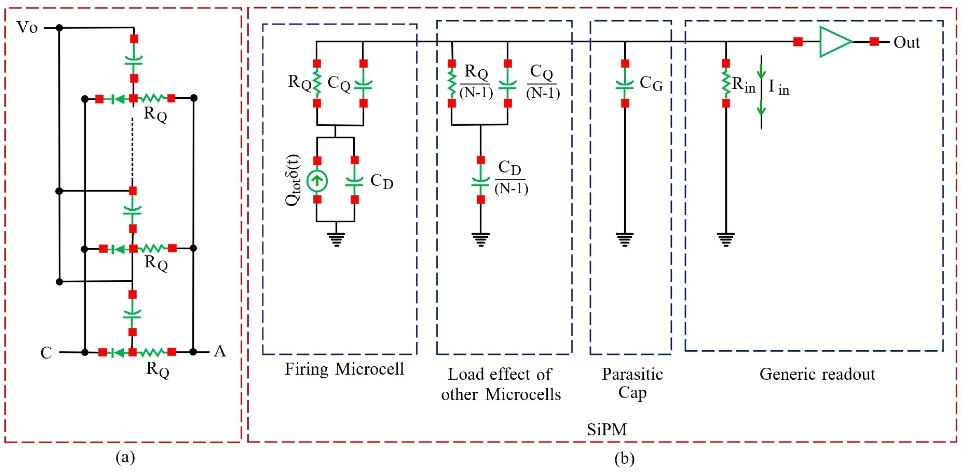
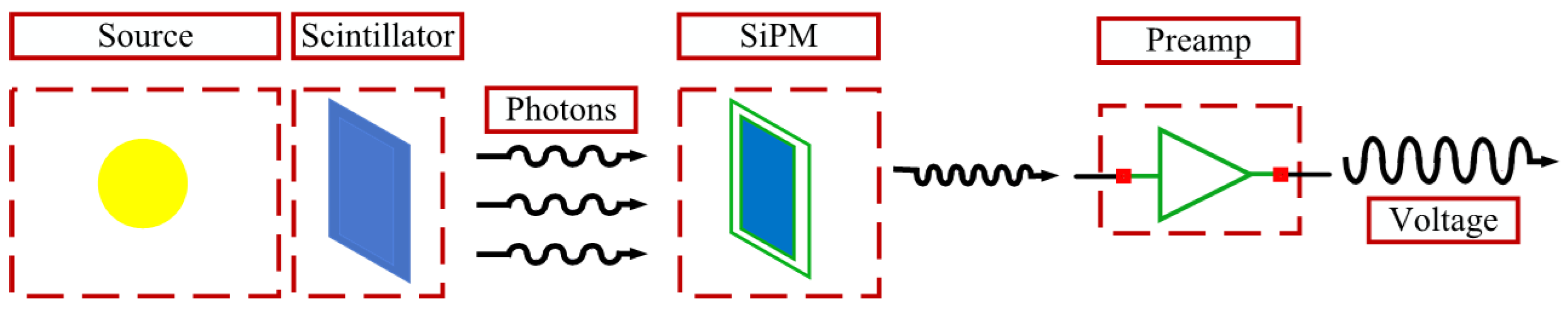
:1. Introduction
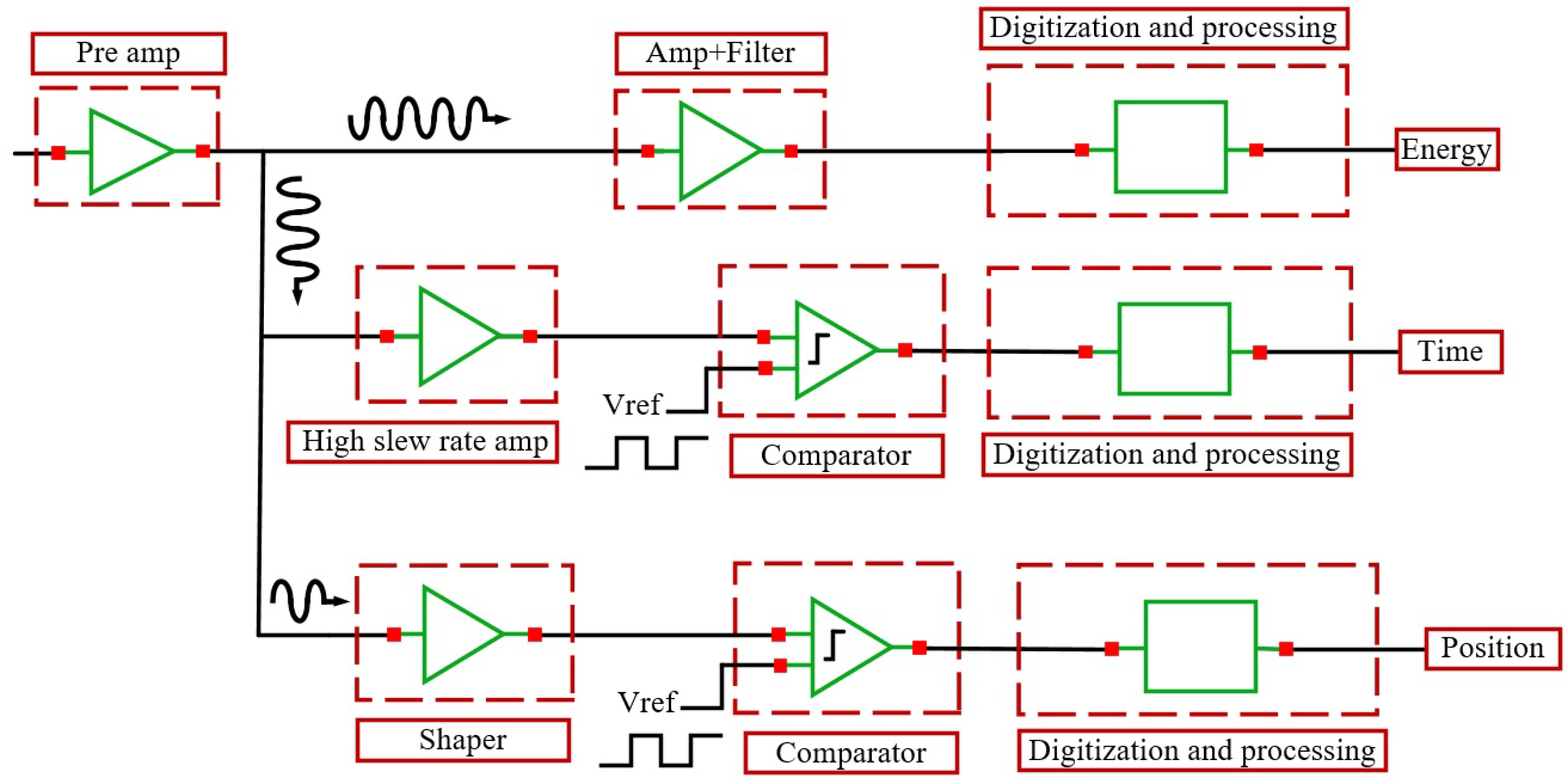
2. Preamplifier Structure in Nuclear Imaging Systems
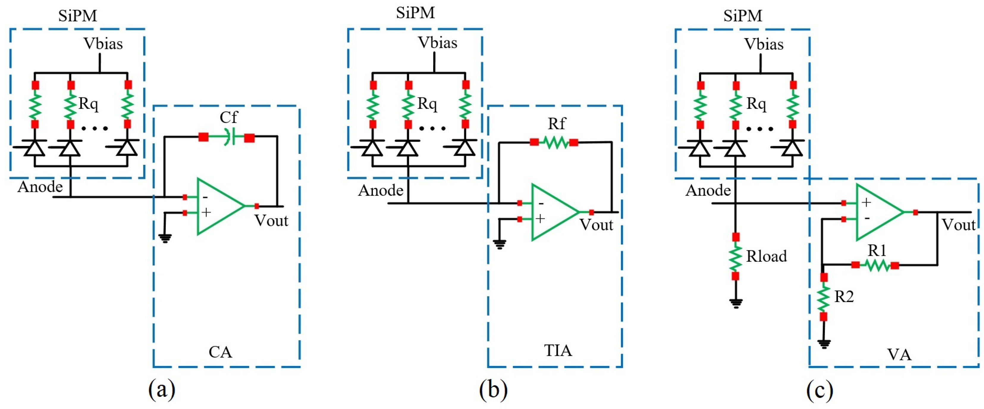
2.1. Charge-Sensitive Preamplifiers (CSP)
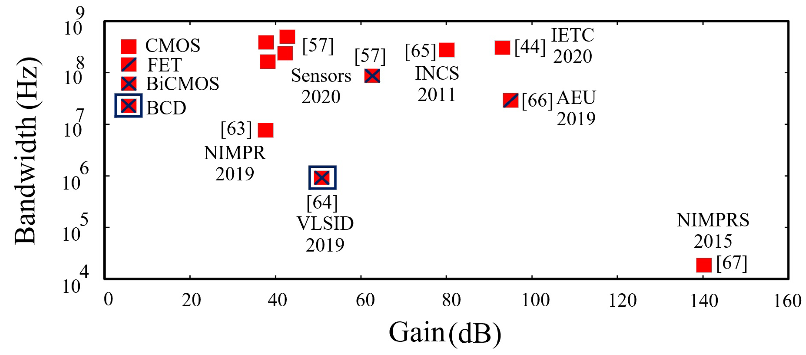
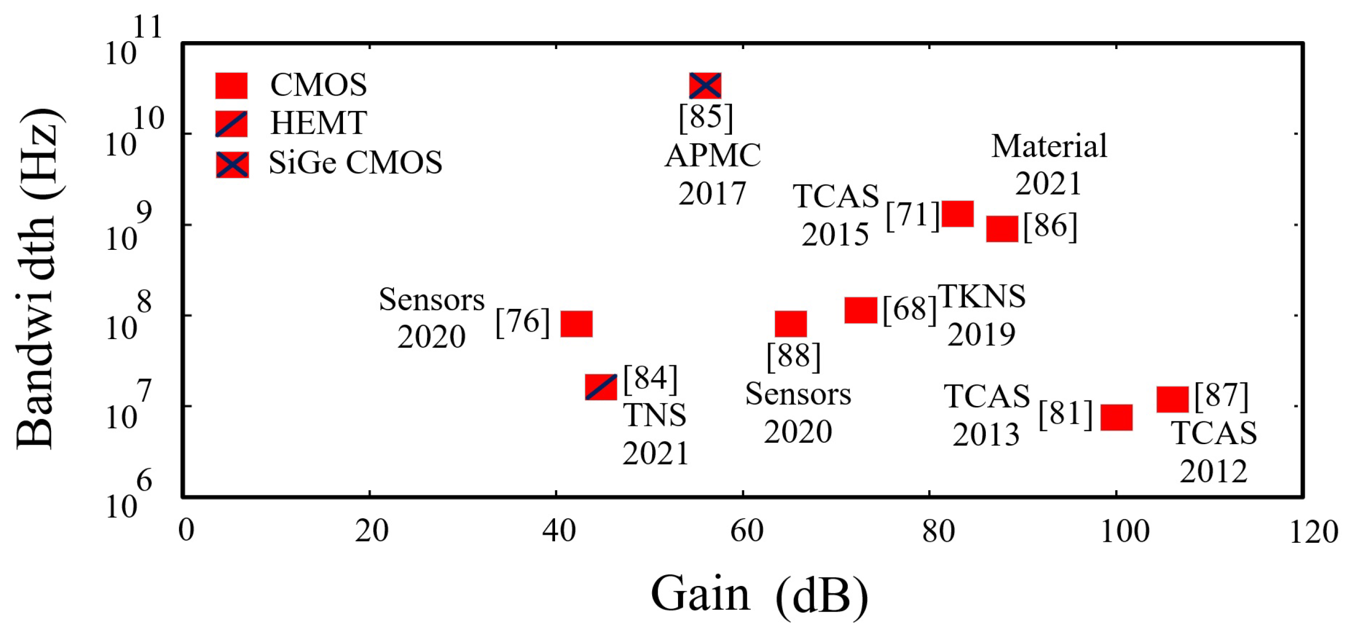
2.2. Transimpedance Preamplifier
2.3. Voltage-Sensitive Preamplifiers
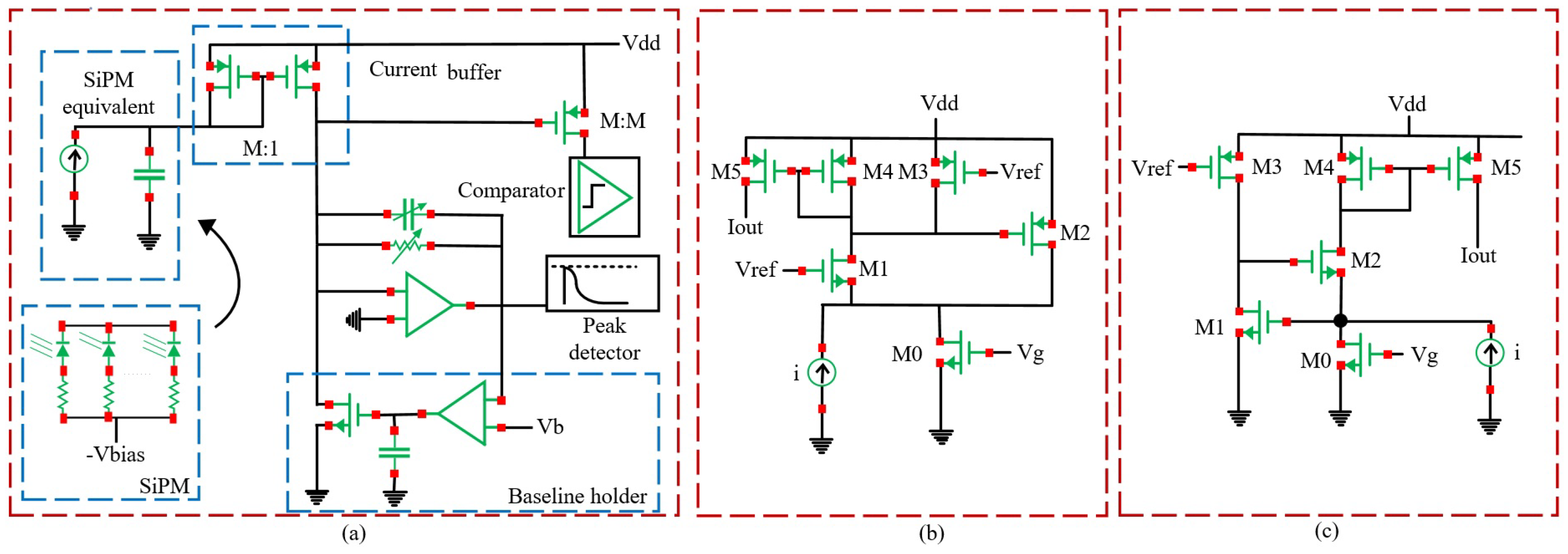
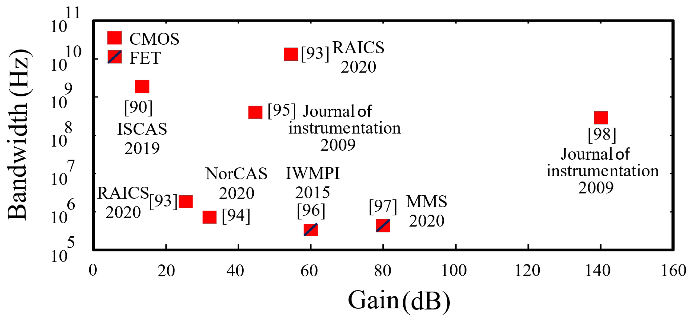
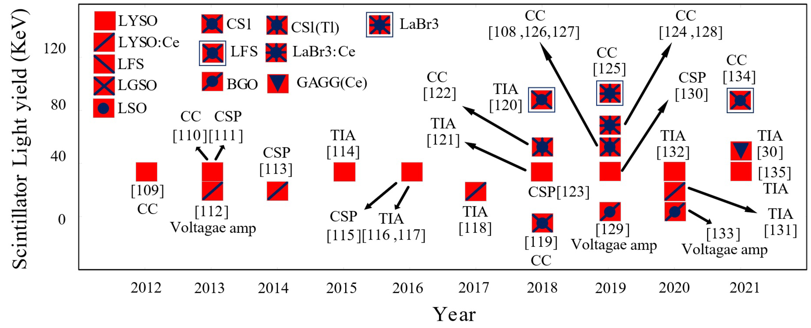
3. Energy Measurements
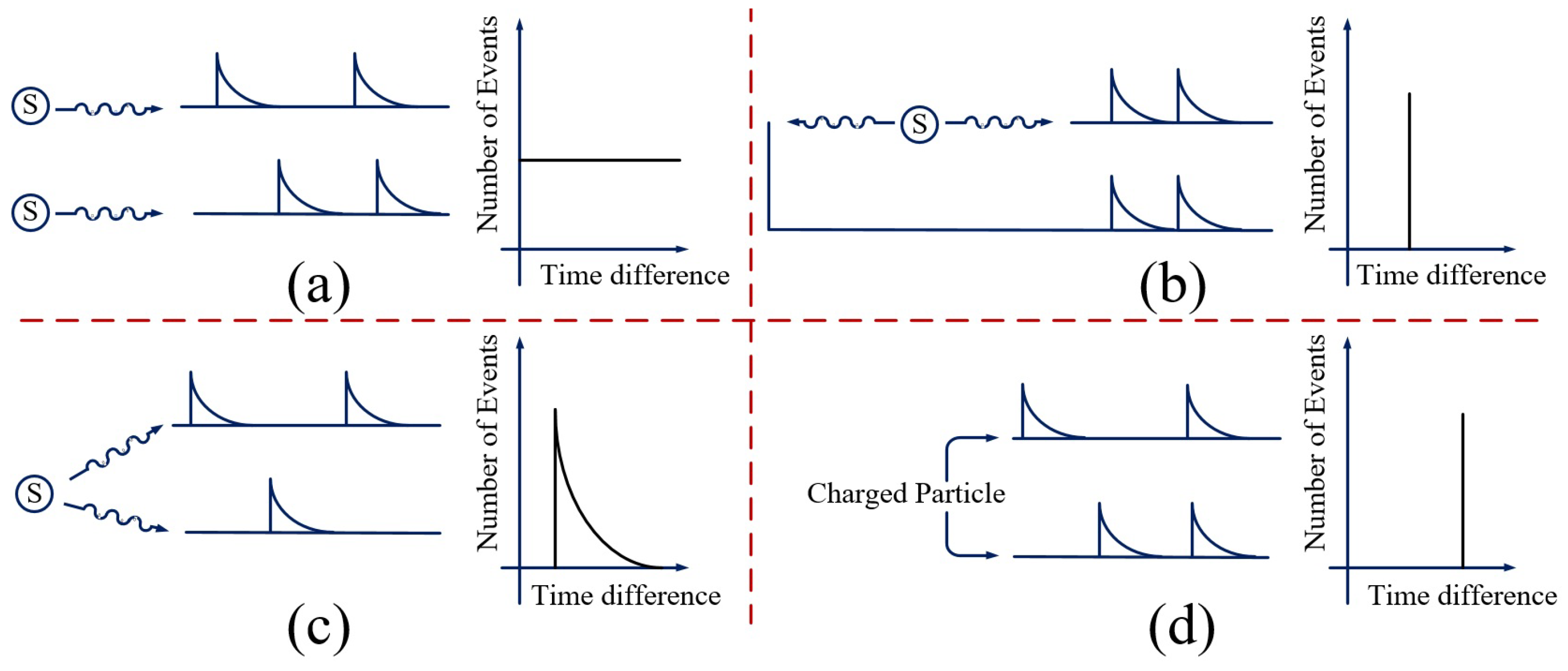
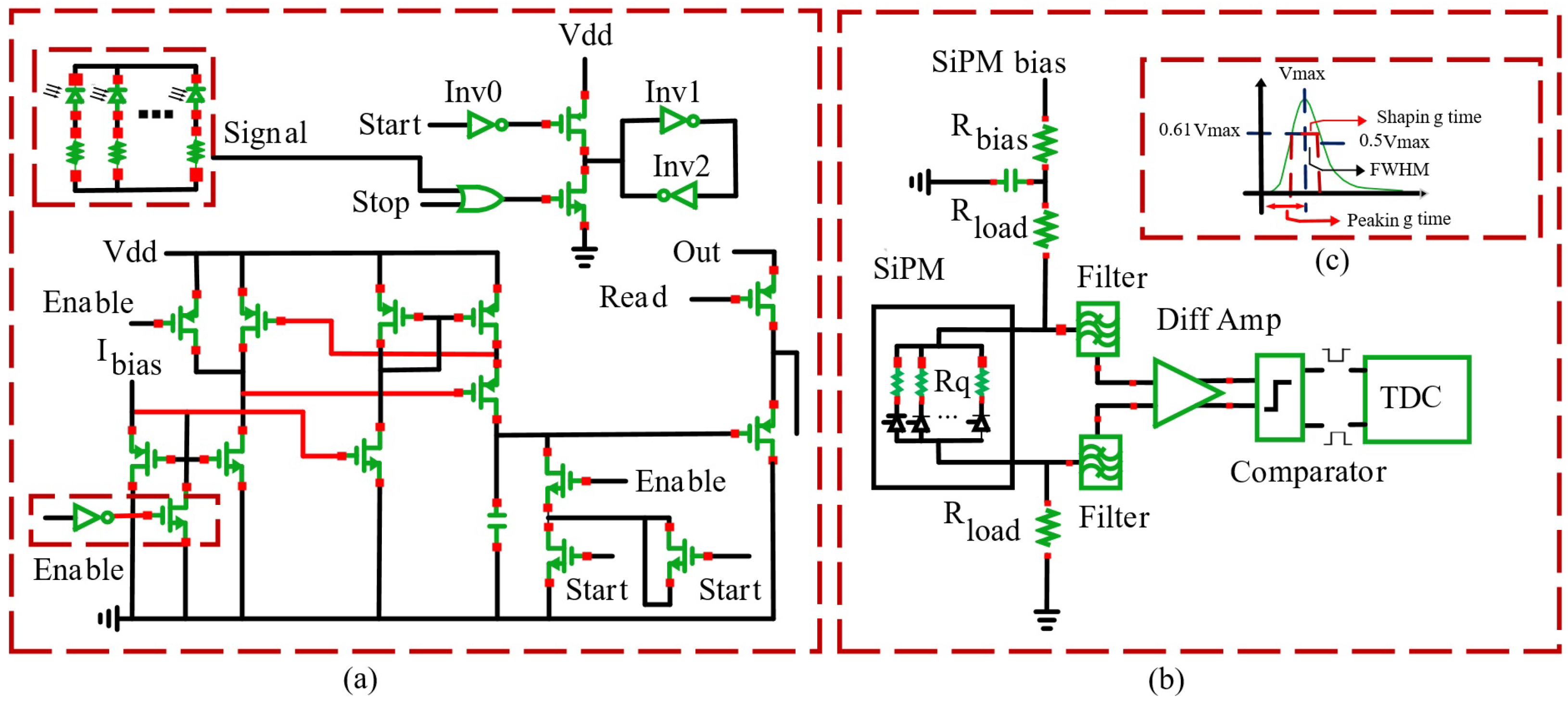
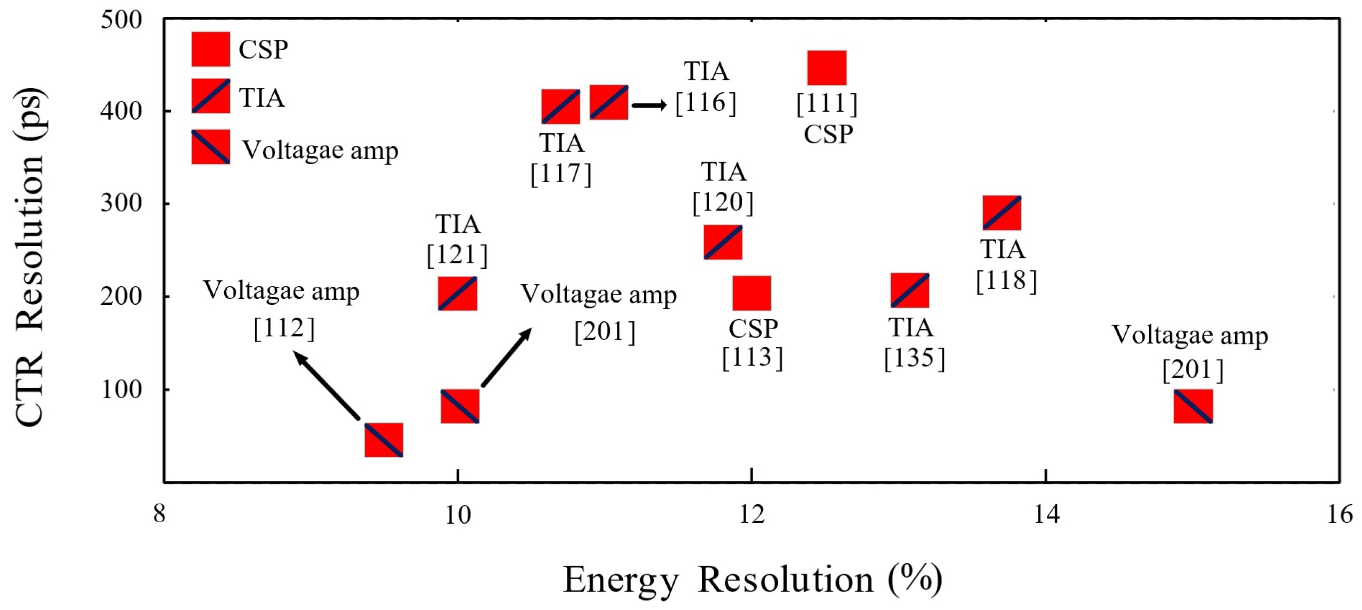
4. Timing Measurements
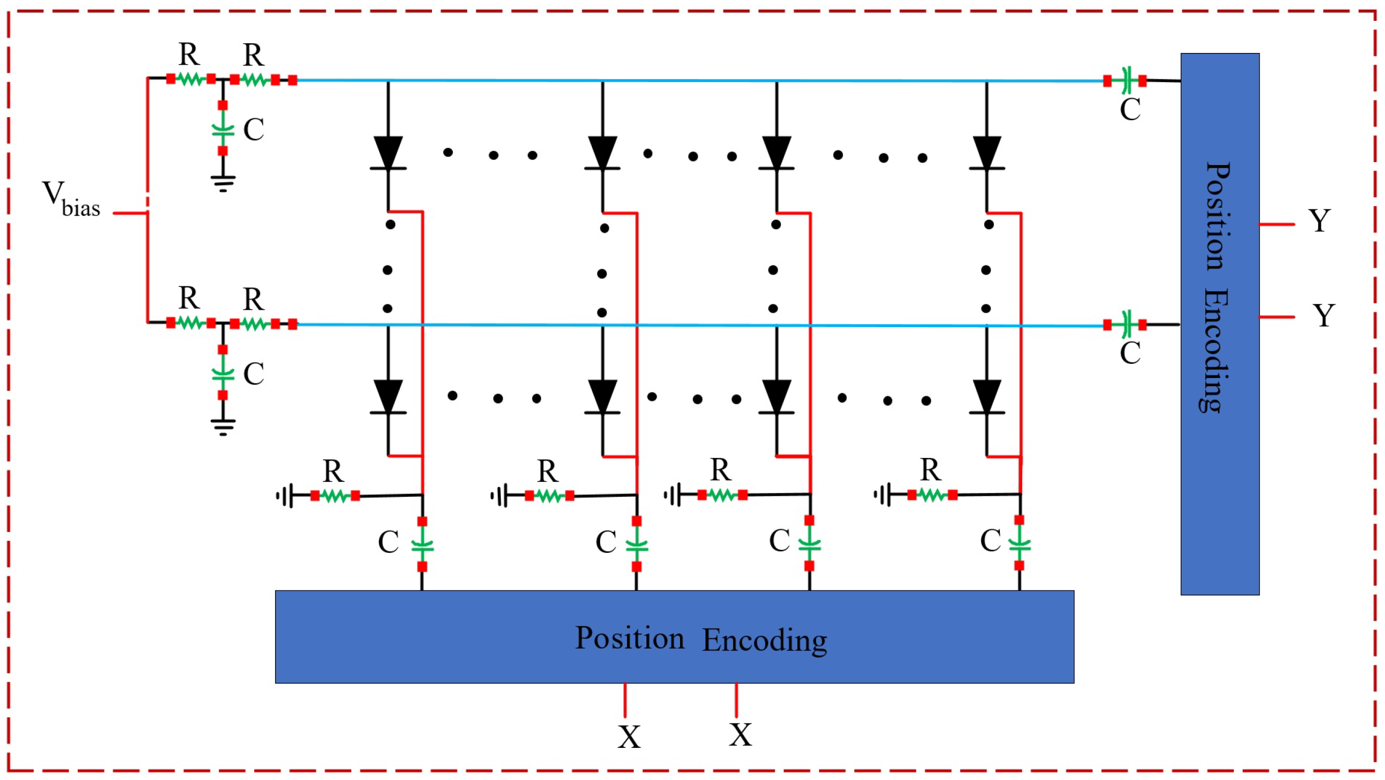
5. Position Sensing
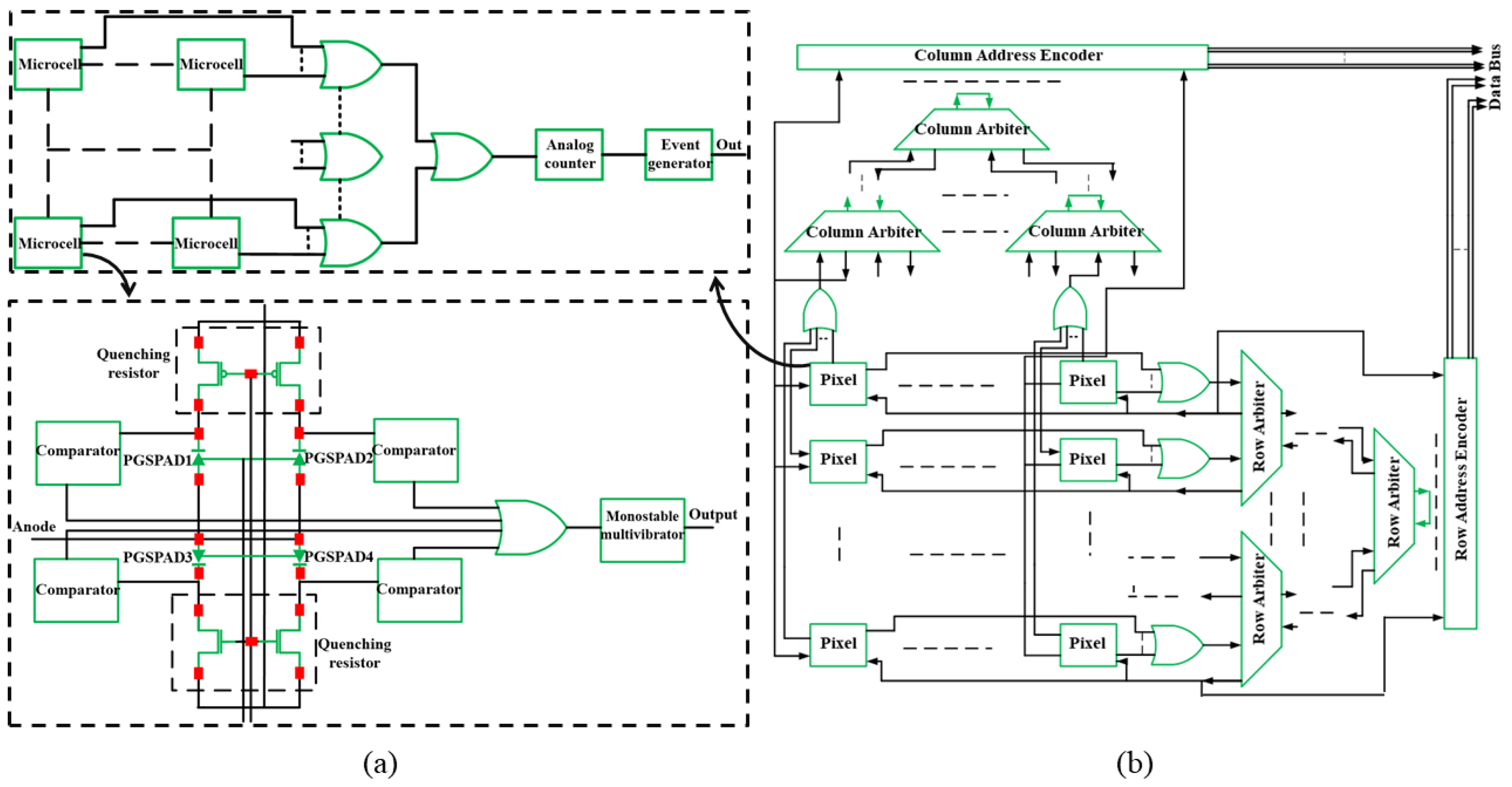
6. Array Readout
7. Conclusions
Author Contributions
Funding
Conflicts of Interest
References
- Alispach, C.; Borkowski, J.; Cadoux, F.R.; De Angelis, N.; Della Volpe, D.; Favre, Y.; Heller, M.; Juryšek, J.; Lyard, E.; Mandat, D.; et al. Large scale characterization and calibration strategy of a SiPM-based camera for gamma-ray astronomy. J. Instrum. 2020, 15, P11010. [Google Scholar] [CrossRef]
- Henningsen, F.; Boehmer, M.; Gärtner, A.; Geilen, L.; Gernhäuser, R.; Heggen, H.; Holzapfel, K.; Fruck, C.; Papp, L.; Rea, I.; et al. A self-monitoring precision calibration light source for large-volume neutrino telescopes. J. Instrum. 2020, 15, P07031. [Google Scholar] [CrossRef]
- Sun, Y.; Maricic, J. SiPMs characterization and selection for the DUNE far detector photon detection system. J. Instrum. 2016, 11, C01078. [Google Scholar] [CrossRef] [Green Version]
- Adamo, G.; Busacca, A. Time Of Flight measurements via two LiDAR systems with SiPM and APD. In Proceedings of the AEIT International Annual Conference, Capri, Italy, 5–7 October 2016; pp. 1–5. [Google Scholar]
- Gnecchi, S.; Buckley, S.; Bellis, S.; Barry, C.; Jackson, C. SiPM sensors for TOF ranging applications. In Proceedings of the SPIE Photonics West, San Francisco, CA, USA, 13–18 February 2016. [Google Scholar]
- Gnecchi, S.; Barry, C.; Bellis, S.; Buckley, S.; Jackson, C. Long Distance Ranging Performance of Gen3 LiDAR Imaging System based on 1 × 16 SiPM Array. In Proceedings of the International Image Sensor Workshop, Snowbird, UT, USA, 23–27 June 2019. [Google Scholar]
- Gnecchi, S.; Jackson, C. A 1 × 16 SiPM array for automotive 3D imaging LiDAR systems. In Proceedings of the International Image Sensor Workshop, Hiroshima, Japan, 30 May–2 June 2017; pp. 133–136. [Google Scholar]
- Jeong, M.; Hammig, M. Development of hand-held coded-aperture gamma ray imaging system based on GAGG (Ce) scintillator coupled with SiPM array. Nucl. Eng. Technol. 2020, 52, 2572–2580. [Google Scholar] [CrossRef]
- Shimazoe, K.; Yoshino, M.; Ohshima, Y.; Uenomachi, M.; Oogane, K.; Orita, T.; Takahashi, H.; Kamada, K.; Yoshikawa, A.; Takahashi, M. Development of simultaneous PET and Compton imaging using GAGG-SiPM based pixel detectors. Nucl. Instrum. Methods Phys. Res. Sect. A Accel. Spectrometers Detect. Assoc. Equip. 2020, 954, 161499. [Google Scholar] [CrossRef]
- Liang, Z.; Hu, T.; Li, X.; Wu, Y.; Li, C.; Tang, Z. A cosmic ray imaging system based on plastic scintillator detector with SiPM readout. J. Instrum. 2020, 15, C07033. [Google Scholar] [CrossRef]
- Maira, G.; Chiarelli, A.M.; Brafa, S.; Libertino, S.; Fallica, G.; Merla, A.; Lombardo, S. Imaging System Based on Silicon Photomultipliers and Light Emitting Diodes for Functional Near-Infrared Spectroscopy. Appl. Sci. 2020, 10, 1068. [Google Scholar] [CrossRef] [Green Version]
- Kitsmiller, V.J.; O’Sullivan, T.D. Next-generation frequency domain diffuse optical imaging systems using silicon photomultipliers. Opt. Lett. 2019, 44, 562–565. [Google Scholar] [CrossRef] [PubMed]
- Dey, S.; Myers, E.; Lewellen, T.K.; Miyaoka, R.S.; Rudell, J.C. A row-column summing readout architecture for SiPM based PET imaging systems. In Proceedings of the IEEE Nuclear Science Symposium and Medical Imaging Conference, Seoul, Korea, 27 October–2 November 2013; pp. 1–5. [Google Scholar]
- Cates, J.W.; Bieniosek, M.F.; Levin, C.S. Highly multiplexed signal readout for a time-of-flight positron emission tomography detector based on silicon photomultipliers. J. Med. Imaging 2017, 4, 011012. [Google Scholar] [CrossRef] [Green Version]
- Kim, H.; Kao, C.M.; Hua, Y.; Xie, Q.; Chen, C.T. Multiplexing Readout for Time-of-Flight (TOF) PET Detectors Using Striplines. IEEE Trans. Radiat. Plasma Med. Sci. 2021. [Google Scholar] [CrossRef]
- Yang, Q.; Kuang, Z.; Sang, Z.; Yang, Y.; Du, J. Performance comparison of two signal multiplexing readouts for SiPM-based pet detector. Phys. Med. Biol. 2019, 64, 23NT02. [Google Scholar] [CrossRef]
- Tétrault, M.A.; Lamy, E.D.; Boisvert, A.; Thibaudeau, C.; Kanoun, M.; Dubois, F.; Fontaine, R.; Pratte, J.F. Real-time discrete SPAD array readout architecture for time of flight PET. IEEE Trans. Nucl. Sci. 2015, 62, 1077–1082. [Google Scholar] [CrossRef] [Green Version]
- Giacomelli, M.G. Evaluation of silicon photomultipliers for multiphoton and laser scanning microscopy. J. Biomed. Opt. 2019, 24, 106503. [Google Scholar] [CrossRef] [Green Version]
- Martin, C.; Li, T.; Hegarty, E.; Zhao, P.; Mondal, S.; Ben-Yakar, A. Line excitation array detection fluorescence microscopy at 0.8 million frames per second. Nat. Commun. 2018, 9, 1–10. [Google Scholar] [CrossRef] [PubMed] [Green Version]
- Dorosz, P.; Baszczyk, M.; Kucewicz, W. The study of single cells in a system based on Silicon Photomultipliers. In Proceedings of the IEEE Nuclear Science Symposium and Medical Imaging Conference, Sydney, NSW, Australia, 10–17 November 2018; pp. 1–2. [Google Scholar]
- Heller, M.; jr Schioppa, E.; Porcelli, A.; Pujadas, I.T.; Zietara, K.; Della Volpe, D.; Montaruli, T.; Cadoux, F.; Favre, Y.; Aguilar, J.; et al. An innovative silicon photomultiplier digitizing camera for gamma-ray astronomy. Eur. Phys. J. C 2017, 77, 1–31. [Google Scholar] [CrossRef] [Green Version]
- Zhang, J.; Zhou, R.; Zhang, S.; Xiong, H.; Hu, G.; Li, Y.; Liu, Z.; Yang, C. Data acquisition and trigger system for imaging atmospheric Cherenkov telescopes of the LHAASO. J. Instrum. 2020, 15, T02004. [Google Scholar] [CrossRef]
- Xiong, H.; Zhou, R.; Chen, J.; Li, Y.; Yang, C.; Bi, B.; Zhang, J.; Zhang, J.; Cao, X.; Zhang, S.; et al. Design and performance of analog circuit for the wide field of view Cherenkov telescope array of LHAASO. Nucl. Instrum. Methods Phys. Res. Sect. A Accel. Spectrometers Detect. Assoc. Equip. 2019, 925, 156–163. [Google Scholar] [CrossRef]
- Berti, A.; Chiavassa, A.; Corti, D.; Depaoli, D.; Di Pierro, F.; Lessio, L.; Mallamaci, M.; Mariotti, M.; Perennes, C.; Rando, R.; et al. Development and test of a SiPM cluster for a SiPM version of the Cherenkov Telescope Array LST camera. Nucl. Instrum. Methods Phys. Res. Sect. A Accel. Spectrometers Detect. Assoc. Equip. 2020, 982, 164373. [Google Scholar] [CrossRef]
- Jiang, S.; Lu, J.; Meng, S.; Ye, F.; Ning, J.; Yi, Q.; Yang, J.; Yang, R.; Yan, X. A prototype of SiPM-based scintillator Compton camera with capacitive multiplexing readout. J. Instrum. 2021, 16, P01027. [Google Scholar] [CrossRef]
- Aldawood, S.; Thirolf, P.; Miani, A.; B ohmer, M.; Dedes, G.; Gernh auser, R.; Lang, C.; Liprandi, S.; Maier, L.; Marinšek, T.; et al. Development of a Compton camera for prompt-gamma medical imaging. Radiat. Phys. Chem. 2017, 140, 190–197. [Google Scholar] [CrossRef]
- Nakamura, Y.; Shimazoe, K.; Takahashi, H.; Yoshimura, S.; Seto, Y.; Kato, S.; Takahashi, M.; Momose, T. Development of a novel handheld intra-operative laparoscopic Compton camera for 18F-Fluoro-2-deoxy-2-D-glucose-guided surgery. Phys. Med. Biol. 2016, 61, 5837. [Google Scholar] [CrossRef] [PubMed]
- Lee, H.; Lee, T.; Lee, W. Development of a Position-Sensitive 4π Compton Camera Based on a Single Segmented Scintillator. IEEE Trans. Nucl. Sci. 2020, 67, 2511–2522. [Google Scholar] [CrossRef]
- Cozzi, G.; Busca, P.; Carminati, M.; Fiorini, C.; Gola, A.; Piemonte, C.; Regazzoni, V. Development of a SiPM-based detection module for prompt gamma imaging in proton therapy. In Proceedings of the IEEE Nuclear Science Symposium, Medical Imaging Conference and Room-Temperature Semiconductor Detector Workshop, Strasbourg, France, 29 October–6 November 2016; pp. 1–5. [Google Scholar]
- Boo, J.; Hammig, M.D.; Jeong, M. Row–Column Readout Method to Mitigate Radiographic-Image Blurring From Multipixel Events in a Coded-Aperture Imaging System. IEEE Trans. Nucl. Sci. 2021, 68, 1175–1183. [Google Scholar] [CrossRef]
- Martinenghi, E.; Di Sieno, L.; Contini, D.; Sanzaro, M.; Pifferi, A.; Dalla Mora, A. Time-resolved single-photon detection module based on silicon photomultiplier: A novel building block for time-correlated measurement systems. Rev. Sci. Instrum. 2016, 87, 073101. [Google Scholar] [CrossRef] [PubMed] [Green Version]
- Li, B.; Miao, Q.; Wang, S.; Hui, D.; Zhao, T.; Liang, K.; Yang, R.; Han, D. Time-correlated photon counting (TCPC) technique based on a photon-number-resolving photodetector. Adv. Photon Count. Tech. X 2016, 9858, 98580L. [Google Scholar]
- Acconcia, G.; Cominelli, A.; Ghioni, M.; Rech, I. Fast fully-integrated front-end circuit to overcome pile-up limits in time-correlated single photon counting with single photon avalanche diodes. Opt. Express 2018, 26, 15398–15410. [Google Scholar] [CrossRef]
- Corsi, F.; Dragone, A.; Marzocca, C.; Del Guerra, A.; Delizia, P.; Dinu, N.; Piemonte, C.; Boscardin, M.; Dalla Betta, G.F. Modelling a silicon photomultiplier (SiPM) as a signal source for optimum front-end design. Nucl. Instrum. Methods Phys. Res. Sect. A Accel. Spectrometers Detect. Assoc. Equip. 2007, 572, 416–418. [Google Scholar] [CrossRef]
- Marano, D.; Belluso, M.; Bonanno, G.; Billotta, S.; Grillo, A.; Garozzo, S.; Romeo, G.; Catalano, O.; La Rosa, G.; Sottile, G.; et al. Silicon photomultipliers electrical model extensive analytical analysis. IEEE Trans. Nucl. Sci. 2013, 61, 23–34. [Google Scholar] [CrossRef]
- Licciulli, F.; Marzocca, C. Parameter Extraction Method for the Electrical Model of a Silicon Photomultiplier. IEEE Trans. Nucl. Sci. 2016, 63, 2517–2526. [Google Scholar] [CrossRef]
- Du, J.; Bai, X.; Gola, A.; Acerbi, F.; Ferri, A.; Piemonte, C.; Yang, Y.; Cherry, S.R. Performance of a high-resolution depth-encoding PET detector module using linearly-graded SiPM arrays. Phys. Med. Biol. 2018, 63, 035035. [Google Scholar] [CrossRef]
- Muntean, A.; Sachdeva, A.; Venialgo, E.; Gnecchi, S.; Palubiak, D.; Jackson, C.; Charbon, E. A fully integrated state-of-the-art analog sipm with on-chip time conversion. In Proceedings of the IEEE Nuclear Science Symposium and Medical Imaging Conference, Sydney, NSW, Australia, 10–17 November 2018; pp. 1–3. [Google Scholar]
- Walker, R.J.; Webster, E.A.; Li, J.; Massari, N.; Henderson, R.K. High fill factor digital silicon photomultiplier structures in 130nm CMOS imaging technology. In Proceedings of the IEEE Nuclear Science Symposium and Medical Imaging Conference Record, Anaheim, CA, USA, 27 October–3 November 2012; pp. 1945–1948. [Google Scholar]
- Paternoster, G.; Ferrario, L.; Acerbi, F.; Gola, A.G.; Bellutti, P. Silicon Photomultipliers Technology at Fondazione Bruno Kessler and 3D Integration Perspectives. In Proceedings of the European Solid-State Device Research Conference, Cracow, Poland, 23–26 September 2019; pp. 50–53. [Google Scholar]
- Vilella, E.; Alonso, O.; Dieguez, A. 3D integration of Geiger-mode avalanche photodiodes aimed to very high fill-factor pixels for future linear colliders. Nucl. Instrum. Methods Phys. Res. Sect. A Accel. Spectrometers Detect. Assoc. Equip. 2013, 731, 103–108. [Google Scholar] [CrossRef] [Green Version]
- Romanchek, G.; Wang, Y.; Marupudi, H.; Abbaszadeh, S. Performance of Optical Coupling Materials in Scintillation Detectors Post Temperature Exposure. Sensors 2020, 20, 6092. [Google Scholar] [CrossRef] [PubMed]
- Saukoski, M.; Aaltonen, L.; Halonen, K.; Salo, T. Fully integrated charge sensitive amplifier for readout of micromechanical capacitive sensors. In Proceedings of the IEEE International Symposium on Circuits and Systems, Kobe, Japan, 23–26 May 2005; pp. 5377–5380. [Google Scholar]
- Song, Y.; Rozsa, J.; Magalhaes, J.; Smith, S.; Karlinsey, B.; Kinnison, W.; Gustafson, E.; Austin, D.; Hawkins, A.R.; Chiang, S.h.W. Design of Common-Mode Feedback for High-Gain Charge Amplifier. In Proceedings of the Intermountain Engineering, Technology and Computing Conference, Orem, UT, USA, 2–3 October 2020; pp. 1–5. [Google Scholar]
- Kmon, P.; Deptuch, G.; Fahim, F.; Grybos, P.; Maj, P.; Szczygiel, R.; Zimmerman, T. Active feedback with leakage current compensation for charge sensitive amplifier used in hybrid pixel detector. IEEE Trans. Nucl. Sci. 2019, 66, 664–673. [Google Scholar] [CrossRef]
- Bassini, R.; Boiano, C.; Pullia, A. A low-noise charge amplifier with fast rise time and active discharge mechanism. IEEE Trans. Nucl. Sci. 2002, 49, 2436–2439. [Google Scholar] [CrossRef]
- Manghisoni, M.; Comotti, D.; Gaioni, L.; Ratti, L.; Re, V. Dynamic compression of the signal in a charge sensitive amplifier: Experimental results. IEEE Trans. Nucl. Sci. 2017, 65, 636–644. [Google Scholar] [CrossRef]
- Alnasser, E. A Novel Low Output Offset Voltage Charge Amplifier for Piezoelectric Sensors. IEEE Sens. J. 2020, 20, 5360–5367. [Google Scholar] [CrossRef]
- Jeong, S.; Shin, D.; Kim, J. A Transformer-Isolated Common-Mode Active EMI Filter Using a Low-cost BJT Amplifier with Feedforward Structure. In Proceedings of theInternational Conference on Power Electronics and ECCE Asia, Busan, Korea, 27–30 May 2019; pp. 2088–2094. [Google Scholar]
- Comer, D.J.; Comer, D.T. Bipolar Junction Transistor Amplifiers. In Fundamentals of Circuits and Filters; CRC Press: Boca Raton, FL, USA, 2018. [Google Scholar]
- Durdaut, P.; Penner, V.; Kirchhof, C.; Quandt, E.; Knochel, R.; Hoft, M. Noise of a JFET charge amplifier for piezoelectric sensors. IEEE Sens. J. 2017, 17, 7364–7371. [Google Scholar] [CrossRef]
- Scandurra, G.; Giusi, G.; Ciofi, C. Single JFET front-end amplifier for low frequency noise measurements with cross correlation-based gain calibration. Electronics 2019, 8, 1197. [Google Scholar] [CrossRef] [Green Version]
- He, Z.; Wang, C.; Fan, G.; Zhou, Y.; Yang, Y. Design of A High Input Impedance OPA with Bi-JFET Technology. In Proceedings of theIEEE International Conference on Electronics Technology, Chengdu, China, 10–13 May 2019; pp. 233–236. [Google Scholar]
- Grybos, P.; Idzik, M.; Swientek, K.; Maj, P. Integrated charge sensitive amplifier with pole-zero cancellation circuit for high rates. In Proceedings of the IEEE International Symposium on Circuits and Systems, Kos, Greece, 21–24 May 2006; p. 4. [Google Scholar]
- Kasinski, K.; Kleczek, R. A flexible, low-noise charge-sensitive amplifier for particle tracking application. In Proceedings of the 2016 MIXDES-23rd International Conference Mixed Design of Integrated Circuits and Systems, Lodz, Poland, 23–25 June 2016; pp. 124–129. [Google Scholar]
- Manghisoni, M.; Comotti, D.; Gaioni, L.; Ratti, L.; Re, V. Dynamic compression of the signal in a charge sensitive amplifier: From concept to design. IEEE Trans. Nucl. Sci. 2015, 62, 2318–2326. [Google Scholar] [CrossRef]
- Lee, C.; Cho, G.; Unruh, T.; Hur, S.; Kwon, I. Integrated circuit design for radiation-hardened charge-sensitive amplifier survived up to 2 Mrad. Sensors 2020, 20, 2765. [Google Scholar] [CrossRef]
- Manghisoni, M.; Ratti, L.; Re, V.; Speziali, V.; Traversi, G.; Fallica, G. Gamma-ray response of SOI bipolar junction transistors for fast, radiation tolerant front-end electronics. Nucl. Instrum. Methods Phys. Res. Sect. A Accel. Spectrometers Detect. Assoc. Equip. 2004, 518, 477–481. [Google Scholar] [CrossRef]
- England, T.D. Silicon-Germanium BiCMOS and Silicon-on-Insulator CMOS Analog Circuits for Extreme Environment Applications. Ph.D. Thesis, Georgia Institute of Technology, Atlanta, GA, USA, 2014. [Google Scholar]
- Harrison, R.R.; Charles, C. A low-power low-noise CMOS amplifier for neural recording applications. IEEE J. Solid-State Circuits 2003, 38, 958–965. [Google Scholar] [CrossRef]
- Giannelli, P.; Calabrese, G.; Frattini, G.; Granato, M.; Capineri, L. A buffered single-supply charge amplifier for high-impedance piezoelectric sensors. IEEE Trans. Instrum. Meas. 2018, 68, 368–376. [Google Scholar] [CrossRef]
- Capra, S.; Pullia, A. Design and Experimental Validation of an Integrated Multichannel Charge Amplifier for Solid-State Detectors With Innovative Spectroscopic Range Booster. IEEE Trans. Nucl. Sci. 2020, 67, 1877–1884. [Google Scholar] [CrossRef]
- Yadav, I.; Shrimali, H. Noise and crosstalk models of the particle detector with zero-pole transformation charge sensitive amplifier. Nucl. Instrumen. Methods Phys. Res. Sect. A Accel. Spectrometers Detect. Assoc. Equip. 2019, 937, 107–116. [Google Scholar] [CrossRef]
- Yadav, I.; Joshi, A.; Ruscino, E.; Liberali, V.; Andreazza, A.; Shrimali, H. Design of a charge sensitive amplifier for silicon particle detector in BCD 180 nm process. In Proceedings of the 2019 32nd International Conference on VLSI Design and 2019 18th International Conference on Embedded Systems, Delhi, India, 5–9 January 2019; pp. 541–542. [Google Scholar]
- Beikahmadi, M.; Mirabbasi, S. A low-power low-noise CMOS charge-sensitive amplifier for capacitive detectors. In Proceedings of the IEEE International New Circuits and Systems Conference, Bordeaux, France, 26–29 June 2011; pp. 450–453. [Google Scholar]
- Gu, Z.; Bi, X. A charge amplifier with noise peaking suppression and gain drop compensation utilizing a Quasi-Miller RC network. AEU-Int. J. Electron. Commun. 2019, 107, 252–256. [Google Scholar] [CrossRef]
- Kwon, I.; Kang, T.; Wells, B.T.; Lawrence, J.; Hammig, M.D. Compensation of the detector capacitance presented to charge-sensitive preamplifiers using the Miller effect. Nucl. Instrum. Methods Phys. Res. Sect. A Accel. Spectrometers Detect. Assoc. Equip. 2015, 784, 220–225. [Google Scholar] [CrossRef]
- Seung, M.; Choi, W.; Hur, S.; Kwon, I. Design of a Transimpedance Amplifier for a Radiation Detector to Observe a Nuclear Reactor under Severe Accidents. In Proceedings of the Transactions of the Korean Nuclear Society Spring Meeting, Jeju, Korea, 23–24 May 2019. [Google Scholar]
- Zocca, F.; Pullia, A.; Pascovici, G. Design and optimization of low-noise wide-bandwidth charge preamplifiers for high purity germanium detectors. IEEE Trans. Nucl. Sci. 2008, 55, 695–702. [Google Scholar] [CrossRef]
- Ip, H.M.; Thomas, S.; Hart, M.; Prydderch, M.; French, M. A dynamic slew correction circuit for low noise silicon detector pre-amplifiers. IEEE Trans. Nucl. Sci. 2012, 59, 642–646. [Google Scholar] [CrossRef]
- Kwon, I.; Kang, T.; Wells, B.T.; Lawrence, J.; Hammig, M.D. A high-gain 1.75-GHz dual-inductor transimpedance amplifier with gate noise suppression for fast radiation detection. IEEE Trans. Circuits Syst. II Express Briefs 2015, 63, 356–360. [Google Scholar] [CrossRef]
- Montenegro, M.V. Front-End CMOS Transimpedance Amplifiers on a Silicon Photomultiplier Resistant to Fast Neutron Fluence. Ph.D. Thesis, University of Nevada, Las Vegas, NV, USA, 2020. [Google Scholar]
- Kaspar, J.; Fienberg, A.; Hertzog, D.; Huehn, M.; Kammel, P.; Khaw, K.; Peterson, D.; Smith, M.; Van Wechel, T.; Chapelain, A.; et al. Design and performance of SiPM-based readout of PbF2 crystals for high-rate, precision timing applications. J. Instrum. 2017, 12, P01009. [Google Scholar] [CrossRef] [Green Version]
- Barile, G.; Leoni, A.; Pantoli, L.; Safari, L.; Stornelli, V. A new VCII based low-power low-voltage front-end for silicon photomultipliers. In Proceedings of the International Conference on Smart and Sustainable Technologies, Split, Croatia, 26–29 June 2018; pp. 1–4. [Google Scholar]
- Pantoli, L.; Barile, G.; Leoni, A.; Muttillo, M.; Stornelli, V. A novel electronic interface for micromachined Si-based photomultipliers. Micromachines 2018, 9, 507. [Google Scholar] [CrossRef] [Green Version]
- Stornelli, V.; Pantoli, L.; Barile, G.; Leoni, A.; D’Amico, E. Silicon Photomultiplier Sensor Interface Based on a Discrete Second Generation Voltage Conveyor. Sensors 2020, 20, 2042. [Google Scholar] [CrossRef] [Green Version]
- Ren, M.; Zhou, J.; Song, B.; Zhang, C.; Dong, M.; Albarracín, R. Towards optical partial discharge detection with micro silicon photomultipliers. Sensors 2017, 17, 2595. [Google Scholar] [CrossRef] [Green Version]
- Naing, T.L.; Rocheleau, T.O.; Alon, E.; Nguyen, C.T.C. A 78-microwatt GSM phase noise-compliant pierce oscillator referenced to a 61-MHz wine-glass disk resonator. In Proceedings of the Joint European Frequency and Time Forum & International Frequency Control Symposium, Prague, Czech Republic, 21–25 July 2013; pp. 562–565. [Google Scholar]
- Elsaegh, S.; Zappe, H.; Manoli, Y.; Klauk, H.; Zschieschang, U. A 1.6 μW tunable organic transimpedance amplifier for photodetector applications based on gain-boosted common-gate input stage and voltage-controlled resistor with ±0.5% nonlinearity. In Proceedings of the European Solid State Circuits Conference, Leuven, Belgium, 11–14 September 2017; pp. 75–78. [Google Scholar]
- Dias, D.C.; de Melo, F.S.; Oliveira, L.B.; Oliveira, J.P. Regulated common-gate transimpedance amplifier for radiation detectors and receivers. In Proceedings of the International Conference Mixed Design of Integrated Circuits and Systems, Lublin, Poland, 19–21 June 2014; pp. 540–545. [Google Scholar]
- de Medeiros Silva, M.; Oliveira, L.B. Regulated common-gate transimpedance amplifier designed to operate with a silicon photo-multiplier at the input. IEEE Trans. Circuits Syst. I Regul. Pap. 2013, 61, 725–735. [Google Scholar] [CrossRef]
- Ambrosi, G.; Ambrosio, M.; Aramo, C.; Bissaldi, E.; Boiano, A.; Bonavolontà, C.; de Lisio, C.; Di Venere, L.; Fiandrini, E.; Giglietto, N.; et al. Development of a Charge Preamplifier to improve NUV-HD SiPM performances. Nucl. Part. Phys. Proc. 2017, 291, 40–43. [Google Scholar] [CrossRef]
- Karimi-Bidhendi, A.; Mohammadnezhad, H.; Green, M.M.; Heydari, P. A silicon-based low-power broadband transimpedance amplifier. IEEE Trans. Circuits Syst. I Regul. Pap. 2017, 65, 498–509. [Google Scholar] [CrossRef]
- Pandey, V.K.; Tan, C.M. Application of Gallium Nitride Technology in Particle Therapy Imaging. IEEE Trans. Nucl. Sci. 2021. [Google Scholar] [CrossRef]
- Giannakopoulos, S.; He, Z.S.; Darwazeh, I.; Zirath, H. Differential common base TIA with 56 dB Ohm gain and 45 GHz bandwidth in 130 nm SiGe. In Proceedings of the IEEE Asia Pacific Microwave Conference, Kuala Lumpur, Malaysia, 13–16 November 2017; pp. 1107–1110. [Google Scholar]
- Kodam, S.; Arashanapalli, A.; Kolla, J.; Dheeraj, G. Design and implementation of CMOS transimpedance amplifier as a photodetector. Mater. Today Proc. 2021. [Google Scholar] [CrossRef]
- Oliveira, L.B.; Leitão, C.M.; Silva, M.M. Noise performance of a regulated cascode transimpedance amplifier for radiation detectors. IEEE Trans. Circuits Syst. I Regul. Pap. 2012, 59, 1841–1848. [Google Scholar] [CrossRef]
- Hesari, S.H.; Hedayatipour, A.; Haque, M.A.; McFarlane, N. A Bulk Driven Transimpedance Amplifier for Portable SiPM Based Detectors. In Proceedings of the 2020 IEEE Sensors, Rotterdam, The Netherlands, 25–28 October 2020; pp. 1–4. [Google Scholar]
- Huizenga, J.; Seifert, S.; Schreuder, F.; Van Dam, H.; Dendooven, P.; L ohner, H.; Vinke, R.; Schaart, D. A fast preamplifier concept for SiPM-based time-of-flight PET detectors. Nucl. Instrum. Methods Phys. Res. Sect. A Accel. Spectrometers Detect. Assoc. Equip. 2012, 695, 379–384. [Google Scholar] [CrossRef]
- Wang, M.; Wang, Y.; Cao, Q.; Wang, L.; Kuang, J.; Xiao, Y. Comparison of three pre-amplifier circuits for time readout of SiPM in TOF-PET detectors. In Proceedings of the International Symposium on Circuits and Systems, Sapporo, Japan, 26–29 May 2019; pp. 1–5. [Google Scholar]
- Argentieri, A.; Corsi, F.; Foresta, M.; Marzocca, C.; Del Guerra, A. Design and characterization of CMOS multichannel front-end electronics for silicon photomultipliers. Nucl. Instrum. Methods Phys. Res. Sect. A Accel. Spectrometers Detect. Assoc. Equip. 2011, 652, 516–519. [Google Scholar] [CrossRef]
- Corsi, F.; Foresta, M.; Marzocca, C.; Matarrese, G.; Del Guerra, A. Current-mode front-end electronics for silicon photo-multiplier detectors. In Proceedings of the International Workshop on Advances in Sensors and Interface, Bari, Italy, 26–27 June 2007; pp. 1–6. [Google Scholar]
- Lakshmy, V.; Shajahan, E. Performance Analysis of Low Power Low Voltage Amplifier Designs in 45 nm CMOS Technology by Incorporating Miller Compensation. In Proceedings of the 2020 IEEE Recent Advances in Intelligent Computational Systems (RAICS), Thiruvananthapuram, India, 3–5 December 2020; pp. 18–22. [Google Scholar]
- Rodovalho, L.H. Schmitt Trigger Based Single-Ended Voltage Amplifier with Positive Feedback Control for Ultra-Low-Voltage Supplies. In Proceedings of the 2020 IEEE Nordic Circuits and Systems Conference (NorCAS), Oslo, Norway, 27–28 October 2020; pp. 1–6. [Google Scholar]
- Dinu, N.; Barrillon, P.; Bazin, C.; Belcari, N.; Bisogni, M.G.; Bondil-Blin, S.; Boscardin, M.; Chaumat, V.; Collazuol, G.; De La Taille, C.; et al. Characteristics of a prototype matrix of Silicon PhotoMultipliers (SiPM). J. Instrum. 2009, 4, P03016. [Google Scholar] [CrossRef] [Green Version]
- Zhang, W.; Zheng, B.; Goodwill, P.; Conolly, S. A custom low-noise preamplifier for Magnetic Particle Imaging. In Proceedings of the 2015 5th International Workshop on Magnetic Particle Imaging (IWMPI), Istanbul, Turkey, 26–28 March 2015; p. 1. [Google Scholar]
- Achtenberg, K.; Mikołajczyk, J.; Bielecki, Z. FET input voltage amplifier for low frequency noise measurements. Metrol. Meas. Syst. 2020, 531–540. [Google Scholar] [CrossRef]
- Corsi, F.; Foresta, M.; Marzocca, C.; Matarrese, G.; Del Guerra, A. ASIC development for SiPM readout. J. Instrum. 2009, 4, P03004. [Google Scholar] [CrossRef]
- Brown, J.M. In-silico optimisation of tileable philips digital SiPM based thin monolithic scintillator detectors for SPECT applications. Appl. Radiat. Isot. 2021, 168, 109368. [Google Scholar] [CrossRef] [PubMed]
- Kim, B.; Lee, K.; Lee, J.; Hwang, S.; Heo, D.; Han, K. Design of optimal digital filter and digital signal processing for a CdZnTe high resolution gamma-ray system. Appl. Radiat. Isot. 2020, 162, 109171. [Google Scholar] [CrossRef]
- Sammartini, M.; Gandola, M.; Mele, F.; Garavelli, B.; Macera, D.; Pozzi, P.; Bertuccio, G. X-ray Spectroscopy with a CdTe Pixel Detector and SIRIO Preamplifier at Deep Submicrosecond Signal-Processing Time. IEEE Trans. Nucl. Sci. 2020, 68, 70–75. [Google Scholar] [CrossRef]
- Lee, M.; Lee, D.; Ko, E.; Park, K.; Kim, J.; Ko, K.; Sharma, M.; Cho, G. Pulse pileup correction method for gamma-ray spectroscopy in high radiation fields. Nucl. Eng. Technol. 2020, 52, 1029–1035. [Google Scholar] [CrossRef]
- Adrich, P.; Zychor, I. Least-squares fitting algorithm for peak pile-up correction in gamma-ray spectroscopy. In Nuclear Instruments and Methods in Physics Research Section A: Accelerators, Spectrometers, Detectors and Associated Equipment; Elsevier: Amsterdam, The Netherlands, 2020; p. 164962. [Google Scholar]
- Pocaterra, M.; Ciappa, M. Experimental setup to monitor non-destructive single events triggered by ionizing radiation in power devices. Microelectron. Reliab. 2020, 114, 113755. [Google Scholar] [CrossRef]
- Ulyanov, A.; Morris, O.; Hanlon, L.; McBreen, S.; Foley, S.; Roberts, O.J.; Tobin, I.; Murphy, D.; Wade, C.; Nelms, N.; et al. Performance of a monolithic LaBr3: Ce crystal coupled to an array of silicon photomultipliers. Nucl. Instrum. Methods Phys. Res. Sect. A Accel. Spectrometers Detect. Assoc. Equip. 2016, 810, 107–119. [Google Scholar] [CrossRef]
- Lavelle, C.; Shanks, W.; Chiang, C.; Nichols, M.; Osborne, J., Jr.; Herschelman, A.; Brown, B.; Cho, M. Approaches for single channel large area silicon photomultiplier array readout. AIP Adv. 2019, 9, 035123. [Google Scholar] [CrossRef] [Green Version]
- Cozzi, G.; Busca, P.; Carminati, M.; Fiorini, C.; Montagnani, G.L.; Acerbi, F.; Gola, A.; Paternoster, G.; Piemonte, C.; Regazzoni, V.; et al. High-Resolution Gamma-Ray Spectroscopy With a SiPM-Based Detection Module for 1” and 2” LaBr 3: Ce Readout. IEEE Trans. Nucl. Sci. 2017, 65, 645–655. [Google Scholar] [CrossRef]
- Montagnani, G.; Buonanno, L.; Di Vita, D.; Carminati, M.; Camera, F.; Gola, A.; Regazzoni, V.; Fiorini, C. Spectroscopic performance of a Sr co-doped 3” LaBr3 scintillator read by a SiPM array. Nucl. Instrum. Methods Phys. Res. Sect. A Accel. Spectrometers Detect. Assoc. Equip. 2019, 931, 158–161. [Google Scholar] [CrossRef]
- Rolo, M.D.; Bugalho, R.; Gonçalves, F.; Rivetti, A.; Mazza, G.; Silva, J.C.; Silva, R.; Varela, J. A 64-channel ASIC for TOFPET applications. In Proceedings of the IEEE Nuclear Science Symposium and Medical Imaging Conference Record, Anaheim, CA, USA, 27 October–3 November 2012; pp. 1460–1464. [Google Scholar]
- Rolo, M.; Bugalho, R.; Goncalves, F.; Mazza, G.; Rivetti, A.; Silva, J.; Silva, R.; Varela, J. Tofpet asic for pet applications. J. Instrum. 2013, 8, C02050. [Google Scholar] [CrossRef]
- Sacco, I.; Fischer, P.; Ritzert, M. PETA4: A multi-channel TDC/ADC ASIC for SiPM readout. J. Instrum. 2013, 8, C12013. [Google Scholar] [CrossRef]
- Fleury, J.; Callier, S.; de La Taille, C.; Seguin, N.; Thienpont, D.; Dulucq, F.; Ahmad, S.; Martin, G. Petiroc, a new front-end ASIC for time of flight application. In Proceedings of the IEEE Nuclear Science Symposium and Medical Imaging Conference, Seoul, Korea, 27 October–2 November 2013; pp. 1–5. [Google Scholar]
- Chen, H.; Briggl, K.; Fischer, P.; Gil, A.; Harion, T.; Munwes, Y.; Ritzert, M.; Schimansky, D.; Schultz-Coulon, H.C.; Shen, W.; et al. A dedicated readout ASIC for time-of-flight positron emission tomography using silicon photomultiplier (SiPM). In Proceedings of the IEEE Nuclear Science Symposium and Medical Imaging Conference, Seattle, WA, USA, 8–15 November 2014; pp. 1–5. [Google Scholar]
- Ahmad, S.; Fleury, J.; de la Taille, C.; Seguin-Moreau, N.; Dulucq, F.; Martin-Chassard, G.; Callier, S.; Thienpont, D.; Raux, L. Triroc: A multi-channel SiPM read-out ASIC for PET/PET-ToF application. IEEE Trans. Nucl. Sci. 2015, 62, 664–668. [Google Scholar] [CrossRef]
- Becker, R.; Casella, C.; Corrodi, S.; Dissertori, G.; Fischer, J.; Howard, A.; Ito, M.; Lustermann, W. Studies of the high rate coincidence timing response of the STiC and TOFPET ASICs for the SAFIR PET scanner. J. Instrum. 2016, 11, P12001. [Google Scholar] [CrossRef]
- Ahmad, S.; de la Taille, C.; Fleury, J.; Seguin-Moreau, N.; Raux, L.; Callier, S.; Martin-Chassard, G.; Dulucq, F.; Thienpont, D. Triroc, a versatile 64-channel SiPM readout ASIC for time-of-flight PET. In Proceedings of the IEEE Nuclear Science Symposium, Medical Imaging Conference and Room-Temperature Semiconductor Detector Workshop, Strasbourg, France, 29 October–6 November 2016; pp. 1–5. [Google Scholar]
- Sportelli, G.; Ahmad, S.; Belcari, N.; Bisogni, M.G.; Camarlinghi, N.; Di Pasquale, A.; Dussoni, S.; Fleury, J.; Morrocchi, M.; Zaccaro, E.; et al. The TRIMAGE PET data acquisition system: Initial results. IEEE Trans. Radiat. Plasma Med Sci. 2016, 1, 168–177. [Google Scholar] [CrossRef]
- Omidvari, N.; Cabello, J.; Topping, G.; Schneider, F.R.; Paul, S.; Schwaiger, M.; Ziegler, S.I. PET performance evaluation of MADPET4: A small animal PET insert for a 7 T MRI scanner. Phys. Med. Biol. 2017, 62, 8671. [Google Scholar] [CrossRef]
- Trigilio, P.; Busca, P.; Quaglia, R.; Occhipinti, M.; Fiorini, C. A SiPM-readout ASIC for SPECT applications. IEEE Trans. Radiat. Plasma Med. Sci. 2018, 2, 404–410. [Google Scholar] [CrossRef]
- Goertzen, A.L.; Van Elburg, D. Performance characterization of MPPC modules for TOF-PET applications. IEEE Trans. Radiat. Plasma Med. Sci. 2018, 3, 475–482. [Google Scholar] [CrossRef]
- Schug, D.; Nadig, V.; Weissler, B.; Gebhardt, P.; Schulz, V. Initial measurements with the PETsys TOFPET2 ASIC evaluation kit and a characterization of the ASIC TDC. IEEE Trans. Radiat. Plasma Med. Sci. 2018, 3, 444–453. [Google Scholar] [CrossRef] [Green Version]
- Carminati, M.; Montagnani, G.L.; Occhipinti, M.; Kuehne, A.; Niendorf, T.; Nagy, K.; Nagy, A.; Czeller, M.; Fiorini, C. SPECT/MRI INSERT compatibility: Assessment, solutions, and design guidelines. IEEE Trans. Radiat. Plasma Med. Sci. 2018, 2, 369–379. [Google Scholar] [CrossRef]
- Zhao, Z.; Xie, S.; Zhang, X.; Yang, J.; Huang, Q.; Xu, J.; Peng, Q. An advanced 100-channel readout system for nuclear imaging. IEEE Trans. Instrum. Meas. 2018, 68, 3200–3210. [Google Scholar] [CrossRef]
- Carminati, M.; Baratelli, F.; Occhipinti, M.; Erlandsson, K.; Nagy, K.; Nyitrai, Z.; Czeller, M.; Kühne, A.; Niendorf, T.; Valtorta, S.; et al. Validation and performance assessment of a preclinical SiPM-based SPECT/MRI insert. IEEE Trans. Radiat. Plasma Med. Sci. 2019, 3, 483–490. [Google Scholar] [CrossRef]
- Buonanno, L.; Montagnani, G.; Di Vita, D.; Castelli, F.; Carminati, M.; Fiorini, C. GAMMA: A High Dynamic Range 16-ch ASIC for Large Scintillators Readout with SiPM Array. In Proceedings of the IEEE Nuclear Science Symposium and Medical Imaging Conference, Manchester, UK, 26 October–2 November 2019; pp. 1–3. [Google Scholar]
- Di Vita, D.; Buonanno, L.; Montagnani, G.; Minerva, A.; Giannoni, A.; Carminati, M.; Camera, F.; Fiorini, C. A High Dynamic Range 144-SiPM Detection Module for Gamma Spectroscopy and Imaging with 3” LaBr 3. In Proceedings of the IEEE Nuclear Science Symposium and Medical Imaging Conference, Manchester, UK, 26 October–2 November 2019; pp. 1–3. [Google Scholar]
- Montagnani, G.L.; Buonanno, L.; Di Vita, D.; Fiorini, C.; Carminati, M. A compact 4-decade dynamic range readout module for gamma spectroscopy and imaging. In Proceedings of the 2019 IEEE International Symposium on Circuits and Systems (ISCAS), Sapporo, Japan, 26–29 May 2019; pp. 1–5. [Google Scholar]
- Carminati, M.; D’Adda, I.; Morahan, A.; Erlandsson, K.; Nagy, K.; Czeller, M.; Tölgyesi, B.; Nyitrai, Z.; Savi, A.; van Mullekom, P.; et al. Clinical SiPM-based MRI-compatible SPECT: Preliminary characterization. IEEE Trans. Radiat. Plasma Med. Sci. 2019, 4, 371–377. [Google Scholar] [CrossRef]
- Yue, X.; Liu, C.; Deng, Z. An Energy-Resolved Photon-Counting Readout Electronics for Scintillator Based on Pole-Zero Compensation and ToT Method. In Proceedings of the IEEE Nuclear Science Symposium and Medical Imaging Conference, Manchester, UK, 26 October–2 November 2019; pp. 1–3. [Google Scholar]
- Cheng, X.; Hu, K.; Shao, Y. Dual-Polarity SiPM Readout Electronics Based on 1-bit Sigma-Delta Modulation Circuit for PET Detector Applications. IEEE Trans. Nucl. Sci. 2019, 66, 2107–2113. [Google Scholar] [CrossRef]
- LaBella, A.; Vaska, P.; Zhao, W.; Goldan, A.H. Convolutional Neural Network for Crystal Identification and Gamma Ray Localization in PET. IEEE Trans. Radiat. Plasma Med. Sci. 2020, 4, 461–469. [Google Scholar] [CrossRef]
- Barrio, J.; Cucarella, N.; Gonzalez, A.J.; Freire, M.; Ilisie, V.; Benlloch, J.M. Characterization of a High-Aspect Ratio Detector With Lateral Sides Readout for Compton PET. IEEE Trans. Radiat. Plasma Med. Sci. 2020, 4, 546–554. [Google Scholar] [CrossRef]
- Kratochwil, N.; Auffray, E.; Gundacker, S. Exploring Cherenkov emission of BGO for TOF-PET. In IEEE Transactions on Radiation and Plasma Medical Sciences; 2020; Early Access, 10 pages; Available online: https://ieeexplore.ieee.org/document/9222347 (accessed on 30 June 2021).
- Sánchez, D.; Gómez, S.; Fernández-Tenllado, J.M.; Ballabriga, R.; Campbell, M.; Gascón, D. Multimodal simulation of large area silicon photomultipliers for time resolution optimization. Nucl. Instrum. Methods Phys. Res. Sect. A Accel. Spectrometers Detect. Assoc. Equip. 2021, 1001, 165247. [Google Scholar] [CrossRef]
- Nadig, V.; Schug, D.; Weissler, B.; Schulz, V. Evaluation of the PETsys TOFPET2 ASIC in multi-channel coincidence experiments. EJNMMI Phys. 2021, 8, 1–21. [Google Scholar] [CrossRef] [PubMed]
- Contino, G.; Catalano, O.; Sottile, G.; Sangiorgi, P.; Capalbi, M.; Osteria, G.; Scotti, V.; Miyamoto, H.; Vigorito, C.; Casolino, M.; et al. An ASIC front-end for fluorescence and Cherenkov light detection with SiPM for space and ground applications. Nucl. Instrum. Methods Phys. Res. Sect. A Accel. Spectrometers Detect. Assoc. Equip. 2020, 980, 164510. [Google Scholar] [CrossRef]
- Molodtsov, S.; Gurbich, A. Simulation of the pulse pile-up effect on the pulse-height spectrum. Nucl. Instrum. Methods Phys. Res. Sect. B Beam Interact. Mater. Atoms 2009, 267, 3484–3487. [Google Scholar] [CrossRef]
- Wu, H.; Xu, H.; Zhang, Q.; Meng, X.; Di, R.; Liu, Y. Implementation of a straight-line shaper on an FPGA for a UAVAGS. J. Instrum. 2020, 15, T10011. [Google Scholar] [CrossRef]
- Liu, Y.; Zhang, J.; Liu, L.; Li, S.; Zhou, R. Implementation of real-time digital CR–RCm shaping filter on FPGA for gamma-ray spectroscopy. Nucl. Instrum. Methods Phys. Res. Sect. A Accel. Spectrometers Detect. Assoc. Equip. 2018, 906, 1–9. [Google Scholar] [CrossRef]
- Kantor, M.Y.; Sidorov, A. Shaping pulses of radiation detectors into a true Gaussian form. J. Instrum. 2019, 14, P01004. [Google Scholar] [CrossRef] [Green Version]
- Zeng, G.; Yang, J.; Hu, T.; Ge, L.; Ouyang, X.; Zhang, Q.; Gu, Y. Baseline restoration technique based on symmetrical zero-area trapezoidal pulse shaper. Nucl. Instrum. Methods Phys. Res. Sect. A Accel. Spectrometers Detect. Assoc. Equip. 2017, 858, 57–61. [Google Scholar] [CrossRef]
- Saxena, S.; Hawari, A.I. Investigation of FPGA-based real-time adaptive digital pulse shaping for high-count-rate applications. IEEE Trans. Nucl. Sci. 2017, 64, 1733–1738. [Google Scholar] [CrossRef]
- Wang, J.; Luo, X.; Wei, X.; Zheng, R.; Feng, C.; Hu, Y. Design of a low-noise, high-linearity, readout ASIC for CdZnTe-based gamma-ray spectrometers. Nucl. Instrum. Methods Phys. Res. Sect. A Accel. Spectrometers Detect. Assoc. Equip. 2021, 988, 164927. [Google Scholar] [CrossRef]
- Zhao, C.; Wang, Z.; Zhao, M.; Yang, C. Characteristics and comparison of two digital quasi-Gauss filters for gamma spectroscopy. J. Instrum. 2021, 16, P01021. [Google Scholar] [CrossRef]
- Saxena, S.; Hawari, A.I. Digital pulse deconvolution with adaptive shaping for real-time high-resolution high-throughput gamma spectroscopy. Nucl. Instrum. Methods Phys. Res. Sect. A Accel. Spectrometers Detect. Assoc. Equip. 2020, 954, 161288. [Google Scholar] [CrossRef]
- Liu, C.; Luo, X.; Zheng, R.; Wang, J.; Wei, X.; Xue, F.; Hu, Y. A low noise APD readout ASIC for electromagnetic calorimeter in HIEPA. Nucl. Instrum. Methods Phys. Res. Sect. A Accel. Spectrometers Detect. Assoc. Equip. 2021, 985, 164686. [Google Scholar] [CrossRef]
- Carminati, M.; Di Vita, D.; Buonanno, L.; Montagnani, G.L.; Fiorini, C. A Lightweight SiPM-Based Gamma-Ray Spectrometer for Environmental Monitoring with Drones. In International Conference on Applications in Electronics Pervading Industry, Environment and Society; Springer: Cham, Switzerland, 2020; pp. 55–61. [Google Scholar]
- Krishnan, S.; Webster, C.; Duffy, A.; Brooks, G.; Clay, R.; Mould, J. Improving the energy resolution while mitigating the effects of dark-noise, for a microcontroller based SiPM sensor. J. Instrum. 2020, 15, P09028. [Google Scholar] [CrossRef]
- Tang, Y.; Zhang, R.; Chen, J. A Low-Power 16-Channel SiPM Readout Front-end with a Shared SAR ADC in 180 nm CMOS. In Proceedings of the International Conference on Solid-State & Integrated Circuit Technology, Kunming, China, 3–6 November 2020; pp. 1–3. [Google Scholar]
- Zhang, H.; Xu, H.; Fan, Y.; Xing, X.; Liu, H.; Wu, J. A time-interleaved pipelined ADC with ultra high speed sampling. Sādhanā 2020, 45, 1–8. [Google Scholar] [CrossRef]
- Wang, H.; Liu, J.; Zhang, H.; Liang, H.; Ye, B. Multiple time-over-threshold readout electronics for fast timing and energy resolving in a SiPM-based positron annihilation lifetime spectrometer. J. Instrum. 2020, 15, P11006. [Google Scholar] [CrossRef]
- Zhu, M.D.; Qin, X.; Wang, L.; Zhang, W.Z.; Lin, Y.; Rong, X.; Du, J. A time-to-digital-converter utilizing bits-counters to decode carry-chains and DSP48E1 slices in a field-programmable-gate-array. J. Instrum. 2021, 16, P02009. [Google Scholar] [CrossRef]
- Pratte, J.F.; Nolet, F.; Parent, S.; Vachon, F.; Roy, N.; Rossignol, T.; Deslandes, K.; Dautet, H.; Fontaine, R.; Charlebois, S.A. 3D Photon-to-Digital Converter for Radiation Instrumentation: Motivation and Future Works. Sensors 2021, 21, 598. [Google Scholar] [CrossRef] [PubMed]
- Gundacker, S.; Heering, A. The silicon photomultiplier: Fundamentals and applications of a modern solid-state photon detector. Phys. Med. Biol. 2020, 65, 17TR01. [Google Scholar] [CrossRef]
- Ullah, M.N.; Park, J.H.; Pratiwi, E.; Kim, G.B.; Yeom, J.Y. Wavelength discrimination (WLD) detector optimization for time-of-flight positron emission tomography with depth of interaction information. Nucl. Instrum. Methods Phys. Res. Sect. A Accel. Spectrometers Detect. Assoc. Equip. 2020, 982, 164498. [Google Scholar] [CrossRef]
- Cates, J.W.; Gundacker, S.; Auffray, E.; Lecoq, P.; Levin, C.S. Improved single photon time resolution for analog SiPMs with front end readout that reduces influence of electronic noise. Phys. Med. Biol. 2018, 63, 185022. [Google Scholar] [CrossRef]
- Nakhostin, M. Signal Processing for Radiation Detectors; John Wiley & Sons: Hoboken, NJ, USA, 2017. [Google Scholar]
- Lecoq, P.; Gundacker, S. SiPM applications in positron emission tomography: Toward ultimate PET time-of-flight resolution. Eur. Phys. J. Plus 2021, 136, 1–16. [Google Scholar] [CrossRef]
- Surti, S.; Karp, J.S. Update on latest advances in time-of-flight PET. Phys. Med. 2020, 80, 251–258. [Google Scholar] [CrossRef]
- Wieczorek, H.; Thon, A.; Dey, T.; Khanin, V.; Rodnyi, P. Analytical model of coincidence resolving time in TOF-PET. Phys. Med. Biol. 2016, 61, 4699. [Google Scholar] [CrossRef] [PubMed]
- Martinazzoli, L.; Kratochwil, N.; Gundacker, S.; Auffray, E. Scintillation properties and timing performance of state-of-the-art Gd3Al2Ga3O12 single crystals. Nucl. Instrum. Methods Phys. Res. Sect. A Accel. Spectrometers Detect. Assoc. Equip. 2021, 1000, 165231. [Google Scholar] [CrossRef]
- Rivetti, A.; Alexeev, M.; Bugalho, R.; Cossio, F.; Rolo, M.D.R.; Di Francesco, A.; Greco, M.; Cheng, W.; Maggiora, M.; Marcello, S.; et al. TIGER: A front-end ASIC for timing and energy measurements with radiation detectors. Nucl. Instrum. Methods Phys. Res. Sect. A Accel. Spectrometers Detect. Assoc. Equip. 2019, 924, 181–186. [Google Scholar] [CrossRef] [Green Version]
- Impiombato, D.; Segreto, A.; Catalano, O.; Giarrusso, S.; Mineo, T. Use of the Peak-Detector mode for gain calibration of SiPM sensors with ASIC CITIROC read-out. J. Instrum. 2020, 15, C04007. [Google Scholar] [CrossRef] [Green Version]
- Parsakordasiabi, M.; Vornicu, I.; Rodríguez-Vázquez, Á.; Carmona-Galán, R. A Low-Resources TDC for Multi-Channel Direct ToF Readout Based on a 28-nm FPGA. Sensors 2021, 21, 308. [Google Scholar] [CrossRef]
- Lobanov, A. Precision timing calorimetry with the CMS HGCAL. J. Instrum. 2020, 15, C07003. [Google Scholar] [CrossRef]
- Susanto, A.T.; Prajitno, P.; Wijaya, S.K.; Soekirno, S.; Susila, I.P. A systematic literature reviews of multichannel analyzer based on FPGA for gamma spectroscopy. J. Phys. Conf. Ser. 2020, 1528, 012016. [Google Scholar] [CrossRef]
- Schmitz, J.A.; Gharzai, M.K.; Balkir, S.; Hoffman, M.W.; Bauer, M. A low-power 10-bit multichannel analyzer chip for radiation detection. In Proceedings of the International Symposium on Circuits and Systems, Baltimore, MD, USA, 28–31 May 2017; pp. 1–4. [Google Scholar]
- Powolny, F.; Auffray, E.; Brunner, S.; Garutti, E.; Goettlich, M.; Hillemanns, H.; Jarron, P.; Lecoq, P.; Meyer, T.; Schultz-Coulon, H.; et al. Time-based readout of a silicon photomultiplier (SiPM) for time of flight positron emission tomography (TOF-PET). IEEE Trans. Nucl. Sci. 2011, 58, 597–604. [Google Scholar] [CrossRef] [Green Version]
- Qin, Z.j.; Chen, C.; Luo, J.s.; Xie, X.h.; Ge, L.q.; Wu, Q.f. A pulse-shape discrimination method for improving Gamma-ray spectrometry based on a new digital shaping filter. Radiat. Phys. Chem. 2018, 145, 193–201. [Google Scholar] [CrossRef]
- Sundberg, C.; Persson, M.U.; Sjölin, M.; Wikner, J.J.; Danielsson, M. Silicon photon-counting detector for full-field CT using an ASIC with adjustable shaping time. J. Med. Imaging 2020, 7, 053503. [Google Scholar] [CrossRef]
- Jogdand, R.R.; Dakhole, P.; Palsodkar, P. Low power flash ADC using multiplexer based encoder. In Proceedings of the International Conference on Innovations in Information, Embedded and Communication Systems, Coimbatore, India, 17–18 March 2017; pp. 1–5. [Google Scholar]
- Pandey, V.K.; Tan, C.M.; Sharma, S. Design of GaN based Comparator Circuit for Radiation Detectors. In Proceedings of the India Council International Conference, New Delhi, India, 10–13 December 2020; pp. 1–6. [Google Scholar]
- Qiu, L.; Wang, K.; Tang, K.; Siek, L.; Zheng, Y. A 10-bit 300 MS/s 5.8 mW SAR ADC with two-stage interpolation for PET imaging. IEEE Sens. J. 2018, 18, 2006–2014. [Google Scholar] [CrossRef]
- Gundacker, S.; Acerbi, F.; Auffray, E.; Ferri, A.; Gola, A.; Nemallapudi, M.; Paternoster, G.; Piemonte, C.; Lecoq, P. State of the art timing in TOF-PET detectors with LuAG, GAGG and L (Y) SO scintillators of various sizes coupled to FBK-SiPMs. J. Instrum. 2016, 11, P08008. [Google Scholar] [CrossRef]
- Gundacker, S.; Turtos, R.; Auffray, E.; Lecoq, P. Precise rise and decay time measurements of inorganic scintillators by means of X-ray and 511 keV excitation. Nucl. Instrum. Methods Phys. Res. Sect. A Accel. Spectrometers Detect. Assoc. Equip. 2018, 891, 42–52. [Google Scholar] [CrossRef]
- Nemallapudi, M.; Gundacker, S.; Lecoq, P.; Auffray, E. Single photon time resolution of state of the art SiPMs. J. Instrum. 2016, 11, P10016. [Google Scholar] [CrossRef]
- Zhang, J.; Knopp, M.I.; Knopp, M.V. Sparse detector configuration in SiPM digital photon counting PET: A feasibility study. Mol. Imaging Biol. 2019, 21, 447–453. [Google Scholar] [CrossRef] [PubMed]
- Cattaneo, P.; De Gerone, M.; Gatti, F.; Nishimura, M.; Ootani, W.; Rossella, M.; Shirabe, S.; Uchiyama, Y. Time resolution of time-of-flight detector based on multiple scintillation counters readout by SiPMs. Nucl. Instrum. Methods Phys. Res. Sect. A Accel. Spectrometers Detect. Assoc. Equip. 2016, 828, 191–200. [Google Scholar] [CrossRef] [Green Version]
- Wu, Z.; Xu, Y.; Ma, Z. A Time-to-Amplitude Converter With High Impedance Switch Topology for Single-Photon Time-of-Flight Measurement. IEEE Access 2021, 9, 16672–16678. [Google Scholar] [CrossRef]
- Ermis, E.; Celiktas, C. Time resolution investigations for general purpose plastic scintillation detectors in different thicknesses. J. Radioanal. Nucl. Chem. 2013, 295, 523–536. [Google Scholar] [CrossRef]
- Akamatsu, G.; Takyu, S.; Yoshida, E.; Iwao, Y.; Tashima, H.; Nishikido, F.; Yamaya, T. Evaluation of a Hamamatsu TOF-PET Detector Module with 3.2 mm Pitch LFS Scintillators and a 256-channel SiPM Array. IEEE Trans. Radiat. Plasma Med. Sci. 2020. [Google Scholar] [CrossRef]
- Sadik, M.; Ai, X.; Lu, Y.; Nock, R. Real-time time correlated photon counters for photon number resolving detectors. Opt. Sens. Detect. VI 2020, 11354, 1135406. [Google Scholar]
- Schaart, D.R. Physics and technology of time-of-flight PET detectors. Phys. Med. Biol. 2021, 66, 09TR01. [Google Scholar] [CrossRef] [PubMed]
- Du, C.M.; Chen, J.D.; Zhang, X.L.; Yang, H.B.; Cheng, K.; Kong, J.; Hu, Z.G.; Sun, Z.Y.; Su, H.; Xu, H.S. Study of time resolution by digital methods with a DRS4 module. Chin. Phys. C 2016, 40, 046101. [Google Scholar] [CrossRef] [Green Version]
- Xu, T.; Wen, J.; Wang, Q.; Wei, Q.; Ma, T.; Liu, Y.; Tai, Y. A novel sub-millimeter resolution PET detector with TOF capability. In Proceedings of the Nuclear Science Symposium and Medical Imaging Conference, Seoul, Korea, 27 October–2 November 2013; pp. 1–5. [Google Scholar]
- Zhang, H.; Wang, X.; Zhang, L.; Zhang, Z. A 10-bit 120-MS/s SAR ADC in 90 nm CMOS with redundancy compensation. In Proceedings of the MTT-S International Wireless Symposium, Chengdu, China, 6–10 May 2018; pp. 1–3. [Google Scholar]
- Bespal’ko, V.; Burak, I.; Salmins, K. Estimating the Precision of a Leading-Edge Discriminator with Amplitude Correction. Instruments Exp. Tech. 2019, 62, 788–793. [Google Scholar] [CrossRef]
- Xie, S.; Zhang, X.; Huang, Q.; Gong, Z.; Xu, J.; Peng, Q. Methods to compensate the time walk errors in timing measurements for PET detectors. IEEE Trans. Radiat. Plasma Med. Sci. 2020, 4, 555–562. [Google Scholar] [CrossRef]
- Oberstedt, A.; Gatera, A.; Göök, A.; Oberstedt, S. Time response and its impact on prompt fission γ-ray spectra characteristics. Eur. Phys. J. A 2020, 56, 1–8. [Google Scholar] [CrossRef]
- Wang, H.; Zhao, Q.; Liang, H.; Gu, B.; Liu, J.; Zhang, H.; Ye, B. A new SiPM-based positron annihilation lifetime spectrometer using LYSO and LFS-3 scintillators. Nucl. Instrum. Methods Phys. Res. Sect. A Accel. Spectrometers Detect. Assoc. Equip. 2020, 960, 163662. [Google Scholar] [CrossRef]
- Calò, P.; Petrignani, S.; Marzocca, C.; Markovic, B.; Dragone, A. A CMOS Front-End for Timing and Charge Readout of Silicon Photomultipliers. In Proceedings of the Nuclear Science Symposium and Medical Imaging Conference, Manchester, UK, 26 October–2 November 2019; pp. 1–5. [Google Scholar]
- Yang, J.; Li, Y.; Tian, Y.; Fu, Y.; Xu, L.; Cai, Y.; Li, Y. Performance optimization of pixelated CdZnTe detector readout by analog ASIC using cathode waveform. J. Instrum. 2020, 15, P04005. [Google Scholar] [CrossRef]
- Yang, Q.; Wang, X.; Kuang, Z.; Zhang, C.; Yang, Y.; Du, J. Evaluation of Two SiPM Arrays for Depth-Encoding PET Detectors Based on Dual-Ended Readout. IEEE Trans. Radiat. Plasma Med. Sci. 2020. [Google Scholar] [CrossRef]
- Abdallah, N.G.; Rashdan, M.; Khalaf, A.A. High Resolution Time-to-digital Converter for PET Imaging. In Proceedings of the International Conference on Innovative Trends in Communication and Computer Engineering, Aswan, Egypt, 8–9 February 2020; pp. 295–298. [Google Scholar]
- Chen, H.; Li, D.D.U. Multichannel, low nonlinearity time-to-digital converters based on 20 and 28 nm FPGAs. IEEE Trans. Ind. Electron. 2018, 66, 3265–3274. [Google Scholar] [CrossRef] [Green Version]
- Gundacker, S.; Auffray, E.; Jarron, P.; Meyer, T.; Lecoq, P. On the comparison of analog and digital SiPM readout in terms of expected timing performance. Nucl. Instrum. Methods Phys. Res. Sect. A Accel. Spectrometers Detect. Assoc. Equip. 2015, 787, 6–11. [Google Scholar] [CrossRef] [Green Version]
- Brogna, A.; D’Andria, F.; Marzocca, C.; Selmani, X.; Weitzel, Q. Time-Performance Design and Study of Ultra-Wideband Amplifiers for SiPM. J. Instrum. 2020, 15, C02015. [Google Scholar] [CrossRef]
- Lecoq, P.; Morel, C.; Prior, J.O.; Visvikis, D.; Gundacker, S.; Auffray, E.; Križan, P.; Turtos, R.M.; Thers, D.; Charbon, E.; et al. Roadmap toward the 10 ps time-of-flight PET challenge. Phys. Med. Biol. 2020, 65, 21RM01. [Google Scholar] [CrossRef] [PubMed]
- Decker, S.M.; Pizzichemi, M.; Polesel, A.; Paganoni, M.; Auffray, E.; Gundacker, S. The Digital-Analog SiPM Approach: A Story of Electronic and Excess Noise. In Proceedings of the IEEE Nuclear Science Symposium and Medical Imaging Conference, Manchester, UK, 26 October–2 November 2019; pp. 1–5. [Google Scholar]
- Kang, H.G.; Yamaya, T.; Han, Y.B.; Song, S.H.; Ko, G.B.; Lee, J.S.; Hong, S.J. Crystal surface and reflector optimization for the SiPM-based dual-ended readout TOF-DOI PET detector. Biomed. Phys. Eng. Express 2020, 6, 065028. [Google Scholar] [CrossRef]
- Lee, M.S.; Cates, J.W.; Kapusta, M.; Schmand, M.; Levin, C.S. Study of Lutetium-based scintillators for PET system design with 100-ps coincidence time resolution. In Proceedings of the IEEE Nuclear Science Symposium and Medical Imaging Conference, Manchester, UK, 26 October–2 November 2019; pp. 1–2. [Google Scholar]
- Berkovich, A.; Datta-Chaudhuri, T.; Abshire, P. A scalable 20 × 20 fully asynchronous SPAD-based imaging sensor with AER readout. In Proceedings of the International Symposium on Circuits and Systems, Lisbon, Portugal, 24–27 May 2015; pp. 1110–1113. [Google Scholar]
- Lin, J.; Andreou, A.G. A 32 × 32 single photon avalanche diode imager with delay-insensitive address-event readout. In Proceedings of the International Symposium of Circuits and Systems, Rio de Janeiro, Brazil, 15–18 May 2011; pp. 1824–1827. [Google Scholar]
- Shawkat, M.S.A.; McFarlane, N. A CMOS Perimeter Gated SPAD Based Digital Silicon Photomultiplier with Asynchronous AER Readout for PET Applications. In Proceedings of the IEEE Biomedical Circuits and Systems Conference, Cleveland, OH, USA, 17–19 October 2018; pp. 1–4. [Google Scholar]
- Shawkat, M.S.A.; Mcfarlane, N. A digital CMOS silicon photomultiplier using perimeter gated single photon avalanche diodes with asynchronous AER readout. IEEE Trans. Circuits Syst. I Regul. Pap. 2020, 67, 4818–4828. [Google Scholar] [CrossRef]
- Leñero-Bardallo, J.A.; Carmona-Galán, R.; Rodríguez-Vázquez, A. Applications of event-based image sensors—Review and analysis. Int. J. Circuit Theory Appl. 2018, 46, 1620–1630. [Google Scholar] [CrossRef]
- Lenero-Bardallo, J.A.; Pérez-Pena, F.; Carmona-Galán, R.; Rodríguez-Vázquez, Á. Pipeline AER arbitration with event aging. In Proceedings of the International Symposium on Circuits and Systems, Baltimore, MD, USA, 28–31 May 2017; pp. 1–4. [Google Scholar]
- Jeong, M.; Van, B.; Wells, B.T.; D’Aries, L.J.; Hammig, M.D. Scalable gamma-ray camera for wide-area search based on silicon photomultipliers array. Rev. Sci. Instrum. 2018, 89, 033106. [Google Scholar] [CrossRef]
- Taheri, A.; Askari, M.; Sasanpour, M. A beta-gamma position-sensitive detector based on rod plastic scintillators and artificial neural networks. J. Instrum. 2020, 15, P06008. [Google Scholar] [CrossRef]
- Peng, Y.; Lv, W.; Dai, L.; Zhao, T.; Liang, K.; Yang, R.; Han, D. A Square-Bordered Position-Sensitive Silicon Photomultiplier Toward Distortion-Free Performance With High Spatial Resolution. IEEE Electron. Device Lett. 2020, 41, 1802–1805. [Google Scholar] [CrossRef]
- Kumar, S.; Herzkamp, M.; Durini, D.; Nöldgen, H.; van Waasen, S. Development of a solid-state position sensitive neutron detector prototype based on 6Li-glass scintillator and digital SiPM arrays. Nucl. Instrum. Methods Phys. Res. Sect. A Accel. Spectrometers Detect. Assoc. Equip. 2020, 954, 161697. [Google Scholar] [CrossRef]
- Du, J.; Bai, X.; Cherry, S.R. A depth-encoding PET detector for high resolution PET using 1 mm SiPMs. Phys. Med. Biol. 2020, 65, 165011. [Google Scholar] [CrossRef] [PubMed]
- Chen, Y.; Deng, Z.; Liu, Y. DIET: A multi-channel SiPM readout ASIC for TOF-PET with individual energy and timing digitizer. J. Instrum. 2018, 13, P07023. [Google Scholar] [CrossRef]
- Zannoni, E.M.; Wilson, M.D.; Bolz, K.; Goede, M.; Lauba, F.; Schöne, D.; Zhang, J.; Veale, M.C.; Verhoeven, M.; Meng, L.J. Development of a multi-detector readout circuitry for ultrahigh energy resolution single-photon imaging applications. Nucl. Instrum. Methods Phys. Res. Sect. A Accel. Spectrometers Detect. Assoc. Equip. 2020, 981, 164531. [Google Scholar] [CrossRef]
- Ljungberg, M.; Pretorius, P.H. SPECT/CT: An update on technological developments and clinical applications. Br. J. Radiol. 2018, 91, 20160402. [Google Scholar] [CrossRef]
- Turecek, D.; Jakubek, J.; Trojanova, E.; Sefc, L. Single layer Compton camera based on Timepix3 technology. J. Instrum. 2020, 15, C01014. [Google Scholar] [CrossRef]
- Attarwala, A.A.; Hardiansyah, D.; Romanó, C.; Jiménez-Franco, L.D.; Roscher, M.; Wängler, B.; Glatting, G. Performance assessment of the ALBIRA II pre-clinical SPECT S102 system for 99 m Tc imaging. Ann. Nucl. Med. 2021, 35, 111–120. [Google Scholar] [CrossRef]
- Sun, X.L.; Wang, H.; Li, X.K.; Cao, G.H.; Kuang, Y.; Zhang, X.C. Monte Carlo computer simulation of a camera system for proton beam range verification in cancer treatment. Future Gener. Comput. Syst. 2020, 102, 978–991. [Google Scholar] [CrossRef]
- Desmonts, C.; Bouthiba, M.A.; Enilorac, B.; Nganoa, C.; Agostini, D.; Aide, N. Evaluation of a new multipurpose whole-body CzT-based camera: comparison with a dual-head Anger camera and first clinical images. EJNMMI Phys. 2020, 7, 1–16. [Google Scholar] [CrossRef]
- Fujieda, K.; Kataoka, J.; Mochizuki, S.; Tagawa, L.; Sato, S.; Tanaka, R.; Matsunaga, K.; Kamiya, T.; Watabe, T.; Kato, H.; et al. First demonstration of portable Compton camera to visualize 223-Ra concentration for radionuclide therapy. Nucl. Instrum. Methods Phys. Res. Sect. A Accel. Spectrometers Detect. Assoc. Equip. 2020, 958, 162802. [Google Scholar] [CrossRef]
- WB Series Silicon Photomultipliers (SiPM)—KETEK GmbH. Available online: https://www.ketek.net/sipm/sipm-modules/tia-modules/ (accessed on 2 April 2021).
- PETsys SiPM Readout System. Available online: https://www.petsyselectronics.com/web/public/products/6 (accessed on 4 February 2021).
- A1702—32-Channel SiPM Readout Front-End Board—CAEN—Tools for Discovery. Available online: https://www.caen.it/products/a1702/ (accessed on 4 February 2021).
- PhotoniQ Multi-Channel Data Acquisition Systems. Available online: https://vertilon.com/pdf/UM6177.pdf (accessed on 4 February 2021).
- SensL, T. Readout Methods for Arrays of Silicon Photomultipliers. Technical Note. 2014. Available online: http://sensl.com/downloads/ds/TN-Readout_Methods_for_Arrays_of_SiPM.pdf (accessed on 4 February 2021).
- Selfridge, A.; Cherry, S.; Badawi, R. Characterization of four readout circuits for an MR compatible, preclinical PET detector. Phys. Med. Biol. 2020, 65, 125008. [Google Scholar] [CrossRef] [PubMed]
- Mihai, C.; Pascovici, G.; Ciocan, G.; Costache, C.; Karayonchev, V.; Lungu, A.; Mărginean, N.; Mihai, R.; Neacşu, C.; Régis, J.M.; et al. Development of large area Silicon Photomultipliers arrays for γ-ray spectroscopy applications. Nucl. Instrum. Methods Phys. Res. Sect. A Accel. Spectrometers Detect. Assoc. Equip. 2020, 953, 163263. [Google Scholar] [CrossRef]
- Poladyan, H.; Bubon, O.; Teymurazyan, A.; Senchurov, S.; Reznik, A. Gaussian position-weighted center of gravity algorithm for multiplexed readout. Phys. Med. Biol. 2020, 65, 165003. [Google Scholar] [CrossRef]
- Jeon, S.J.; Lee, J.S.; Hong, S.H.; Kim, D.H.; Choi, Y.W. Analysis of position error generated in readout resistive network for gamma-ray detection system. In Proceedings of the International Conference on Electronics, Information, and Communication, Barcelona, Spain, 19–22 January 2020; pp. 1–3. [Google Scholar]
- Boo, J.; Hammig, M.; Jeong, M. Hand-held Dual-particle Imager Implemented with a Multiplexed Low Sampling-rate Readout of a SiPM-based Pixelated Stilbene Array. Res. Sq. 2020. [Google Scholar] [CrossRef]
- Liang, X.; Li, J.; Antonecchia, E.; Ling, Y.; Li, Z.; Xiao, W.; Chu, Q.; Wan, L.; Hu, X.; Han, S.; et al. NEMA-2008 and in-vivo animal and plant imaging performance of the large FOV preclinical digital PET/CT system discoverist 180. IEEE Trans. Radiat. Plasma Med. Sci. 2020, 4, 622–629. [Google Scholar] [CrossRef]
- Du, J.; Schmall, J.P.; Di, K.; Yang, Y.; Dokhale, P.A.; Shah, K.S.; Cherry, S.R. Performance comparison of different readouts for position-sensitive solid-state photomultiplier arrays. Biomed. Phys. Eng. Express 2017, 3, 045019. [Google Scholar] [CrossRef] [PubMed]
- Sajedi, S.; Zeraatkar, N.; Taheri, M.; Kaviani, S.; Khanmohammadi, H.; Sarkar, S.; Sabet, H.; Ay, M.R. Generic high resolution PET detector block using 12 × 12 SiPM array. Biomed. Phys. Eng. Express 2018, 4, 035014. [Google Scholar] [CrossRef]


| Reference | [105] (2016) | [106] (2019) | [107] (2017) | [108] (2019) | [108] (2019) |
|---|---|---|---|---|---|
| Scintillator | LaBr3:Ce | CeBr3 | LaBr3(Ce) | LaBr3(Ce) | LaBr3(Ce) co-doped with Sr |
| SiPM | Custom | SensL | FBK | FBK | FBK |
| Resolution | % 4 | % 4.54 | % 3.19 | % 3.4 | % 2.6 |
| at 661 KeV | at 661 keV | at 661 keV | at 661 keV | at 661 keV |
Publisher’s Note: MDPI stays neutral with regard to jurisdictional claims in published maps and institutional affiliations. |
© 2021 by the authors. Licensee MDPI, Basel, Switzerland. This article is an open access article distributed under the terms and conditions of the Creative Commons Attribution (CC BY) license (https://creativecommons.org/licenses/by/4.0/).
Share and Cite
Hatefi Hesari, S.; Haque, M.A.; McFarlane, N. A Comprehensive Survey of Readout Strategies for SiPMs Used in Nuclear Imaging Systems. Photonics 2021, 8, 266. https://doi.org/10.3390/photonics8070266
Hatefi Hesari S, Haque MA, McFarlane N. A Comprehensive Survey of Readout Strategies for SiPMs Used in Nuclear Imaging Systems. Photonics. 2021; 8(7):266. https://doi.org/10.3390/photonics8070266
Chicago/Turabian StyleHatefi Hesari, Shahram, Mohammad Aminul Haque, and Nicole McFarlane. 2021. "A Comprehensive Survey of Readout Strategies for SiPMs Used in Nuclear Imaging Systems" Photonics 8, no. 7: 266. https://doi.org/10.3390/photonics8070266