Article

Near Unity PLQY and High Stability of Barium Thiocyanate Based All-Inorganic Perovskites and Their Applications in White Light-Emitting Diodes

Department of Physics and Engineering Physics, The University of Tulsa, Tulsa, OK 74104, USA
*
Author to whom correspondence should be addressed.
Photonics 2021, 8(6), 209; https://doi.org/10.3390/photonics8060209
Submission received: 21 May 2021 / Revised: 6 June 2021 / Accepted: 8 June 2021 / Published: 9 June 2021
(This article belongs to the Special Issue Wide Bandgap Semiconductor Photonic Devices)

Abstract

:
All-inorganic lead halide perovskite (CsPbX3) nanocrystals (NCs) have emerged as a highly promising new generation of light emitters due to their extraordinary photophysical properties. However, the performance of these semiconducting NCs is undermined due to the inherent toxicity of lead and long-term environmental stability. Here, we report the addition of B-site cation and X-site anion (pseudo-halide) concurrently using Ba(SCN)2 (≤50%) in CsPbX3 NCs to reduce the lead and improve the photophysical properties and stability. The as-grown particles demonstrated an analogous structure with an almost identical lattice constant and a fluctuation of particle size without altering the morphology of particles. Photoluminescence quantum yield is enhanced up to near unity (~98%) by taking advantage of concomitant doping at the B- and X-site of the structure. Benefitted from the defect reductions and stronger bonding interaction between Pb2+ and SCN ions, Ba(SCN)2-based NCs exhibit improved stability towards air and moisture compared to the host NCs. The doped NCs retain higher PLQY (as high as seven times) compared to the host NCs) when stored in an ambient atmosphere for more than 176 days. A novel 3D-printed multiplex color conversion layer was used to fabricate a white light-emitting diode (LED). The obtained white light shows a correlated color temperature of 6764 K, a color rendering index of 87, and luminous efficacy of radiation of 333 lm/W. In summary, this work proposes a facile route to treat sensitive lead halide perovskite NCs and to fabricate LEDs by using a low-cost large-scale 3-D printing method, which would serve as a foundation for fabricating high-quality optoelectronic devices for near future lighting technologies.

Graphical Abstract

1. Introduction

All-inorganic lead halide perovskite nanocrystals (NCs) have attracted significant attention over the past several years due to their astounding optoelectronic properties and economical solution-based processability. These properties render them a champion in modern optoelectronic devices, such as solar cells, light-emitting diodes (LEDs), field-effect transistors, photodetectors, lasers, scintillators, and other optoelectronic devices [1,2,3,4,5,6,7]. In addition, they exhibited attractive photophysical properties, such as high defect tolerance, narrow emission linewidth, high photoluminescence quantum yield (PLQY), and a wide color gamut, which all are highly desirable properties for lighting applications, particularly for fabrication of white LEDs [5,8,9,10,11,12,13]. To date, studies have reported perovskite-based white LEDs with superior optoelectronic properties compared to conventional phosphor-based white LEDs (WLEDs) [1,14,15]. Despite promising applications, a significant gap remains for commercial translations due to the presence of lead—a highly toxic element, and their fragile/easily morphable perovskite lattices and downgraded photoluminescence (PL) in an ambient environment. To fill this gap, it is imperative to develop lead-reduced/lead-free and highly stable metal halide perovskites.
Many researchers have been striving to obtain lead-free halide perovskites by searching for non-toxic elements with a suitable bandgap to replace lead while preserving and improving their optoelectronic properties [6,16,17,18]. Element doping seems to be a promising technique for addressing the root causes of both toxicity and stability issues [6,19,20]. In this regard, elements belonging to the same group (IV) as Pb2+, such as Sn2+ and Ge2+, seem to be most promising to eliminate Pb2+ [21]. However, rapid oxidation of Sn2+ and Ge2+ in the ambient atmosphere restricts the fabrication of high-quality devices. As a result, other guest cations, such as Mn2+, Sr2+, Zn2+, Mg2+, and Eu2+ have been introduced as possible substituents to Pb2+ in halide perovskites [16,22,23,24,25]. Besides, the lead reducing effect, theoretical and experimental studies on the introduction of other less or non-toxic cations at the Pb-site have helped improve the stability of the materials. Recently, Xiang et al. reported an experiment in which up to 40% of Ba2+ was added to CsPbBr3, and the photovoltaic performance was studied. They found that with only 20% of Ba2+ in the host particle, the addition of Ba2+ increases the radiative recombination and stability of the halide perovskite [26]. Bahadur et al. and Chan et al. also used Ba2+ as a doping cation for lead halide perovskite and reported enhanced stability and photovoltaic performance [27,28]. Besides, the partial replacement of halides with pseudo-halide ion (thiocyanate, SCN) into ABX3 perovskites was found beneficial towards the structural stability of halide perovskites against air and moisture [29]. Jiang et al., for the first time, reported that partial replacement of halides with SCN results in increased stability of the metal halide perovskites structure [30]. Since then, a few other studies have reported enhanced luminescent properties, stability, and device performance of SCN-based perovskites [31,32,33]. Given the huge incentive for improving material stability to meet commercial applications, studies have focused on blending NCs with polymers for encapsulation [34]. Kovalenko’s group has used methyl methacrylate to embed NCs and reported enhanced stability [8]. Similarly, others have reported highly stable perovskite-polymer composites in which the luminous properties were not subjected to degradation [35,36,37]. However, the intrinsic limitations of easily malleable ionic crystal lattices of metal halide perovskite NCs were not addressed by such surface-modified approaches. The incompetences of these different approaches in improving the desired stability and reducing the toxicity concurrently under a single synthesis method was challenged by investigating the possible effect of concomitant doping on the B-site and X-site of the perovskite lattice. In this study, we utilize the favorability of Ba2+ and SCN ions to form the environmentally friendly and chemically stable perovskite structure and studied their corresponding effects.
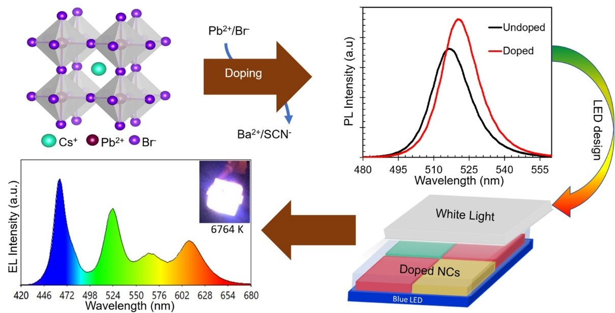
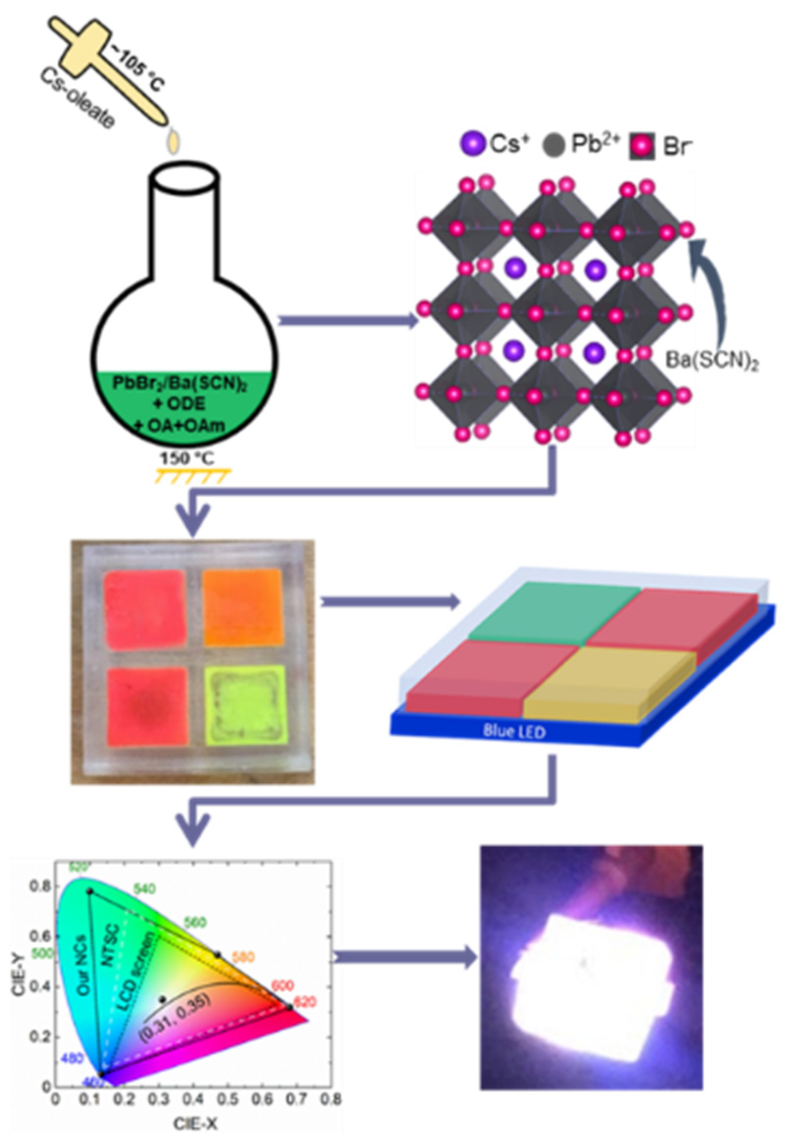
Herein, for the first time, we studied a new series of perovskite composites by introducing Ba(SCN)2 as a dopant for the all-inorganic lead halide perovskite. We explored the effect of Ba(SCN)2 with varying molar ratios (0–50%) on CsPbBr3 by studying its crystal structure, morphology, and optical properties and investigated the performance of designed LEDs. The schematic diagram illustrating the synthesis of NCs and their applications in WLEDs is shown in Figure 1. The addition of dopants did not change the crystal structure explicitly; however, we noticed the change in crystal parameters, including the microstrain and dislocation density. This variation in crystal parameters affected the particle size; however, the morphology remained identical. Furthermore, a variation in optical properties is observed. The bandgap energy and PL emission peak position are altered. PLQY is boosted to near unity (98%), and prolonged air and moisture stability (+176 days) is observed. To investigate the performance of these NCs in a device, a white LED is fabricated using a 3D printer (with clear UV resin) using a single conversion layer that has a multiplex design. Three different colors emitting NCs (green, yellow, and red) are used as down-converting phosphors and stacked on top of blue LED chips. As a result, white light with a correlated color temperature (CCT) of 6764 K, a color rendering index (CRI) of 87, and luminous efficacy of radiation (LER) of 333 lm/W is produced. This ingenious design eliminates the reabsorption of light from the phosphors, which generally arise in the multi-layers, and makes the fabrication of LEDs easier by eliminating the cumbersome preparation process of multi-layers. This new technique may open a new direction for both scientific research studies and future lighting applications.

2. Materials and Methods

2.1. Synthesis of Ba(SCN)2 Added CsPbX3 NCs

A modified hot-injection method was adopted for the synthesis of Ba(SCN)2 alloyed CsPbX3 NCs. Briefly, the Cs-oleate precursor was prepared by mixing 0.448 g of cesium carbonate (Cs2CO3) with 1.375 mL of oleic acid (OA) and 22 mL of octadecene (ODE) in a 50 mL flask. The mixture was dried under vacuum for 1 h at 120 °C and then heated under N2 at 140 °C until all Cs2CO3 had reacted with OA. Then, 0.188 mmol of PbX2 and 0.188 mmol of Ba(SCN)2 were loaded separately in a 25 mL flask with 5 mL of ODE, 0.5 mL of OA, and 0.5 mL of oleylamine, and dried under vacuum for 1 h at 120 °C. These individual mixtures were stirred at the desired growth temperature (140 °C) until the corresponding salts dissolved completely. The preheated 0.4 mL of Cs-oleate solution (120 °C before injection) was quickly injected into the solution obtained by mixing proportionate amounts of PbX2 and Ba(SCN)2 precursors. After 2–5 s of heating the mixture, the flask containing the mixture was quickly placed in an ice-water bath, allowing it to cool for ~3 min. The resulting crude solution was centrifuged at 3500 rpm for 10 min. The clear supernatant was discarded, and the precipitates were re-dispersed in toluene/hexane for further characterization and long-term storage. Similarly, at 50% of Ba(SCN)2, different compositions of halides (Br and I) were mixed to obtain the desired emissions across the visible region.

2.2. White LED Fabrication

To prevent a possible anion exchange in the mixture of different halides, we printed a partitioned box (four small boxes confined in a single big box) to confine the NCs separately. A Formlabs Form 3 printer filled with transparent UV resin input material was used. Each partitioned box has a dimension of 9 mm × 7 mm. An equal amount of colloidal solutions (suspended in 1 mL of hexane) of three different colors emitting NCs (green, yellow, and red) were dropped into the individual compartment. The box was then kept in a vacuum at room temperature (~25 °C) for 20 mins to remove the solvent and forming a thin layer of NCs. After drying the samples, the epoxy resin (a mixture of resin and hardener in equal ratio) was dropped on the NCs (acts as the cover for the box) to prevent external contact with air and moisture. Finally, the structure was stacked on top of the blue LEDs (λ ~ 460 nm, runs at 3.97 mA and 7.50 V) to obtain white light.

2.3. Characterization

A Rigaku SmartLab Diffractometer with CuKα1 radiation, λ = 1.54 Å operated at 40 kV and 44 mA, and at an angular range (2θ) with a step of 0.01° was employed to measure X-ray diffraction (XRD) patterns. For Transmission Electron Microscopy (TEM) images, a Hitachi H-7000 transmission microscope operated at 75 kV was used. The PL spectra and the UV–vis spectra were measured using the Spectro-Fluorophotometer (Shimadzu, RF6000) and the Varian Carry 50 Scan UV spectrophotometer, respectively. The PLQYs were measured using the QE-pro spectrometer (QEP02037, Ocean Optics) coupled with an integrating sphere (819C-SF-6, Newport) excited using a laser source at a wavelength of 405 nm. The electroluminescent (EL) spectra were recorded with a QE-pro spectrometer (QEP02037, Ocean Optics) in conjunction with 460 nm blue LED chips and a Keithley 2450 source meter operated at 3.97 mA and 7.50 V under a forward bias as a source for LED chips. All the spectra measurements were performed at room temperature.

3. Results and Discussion

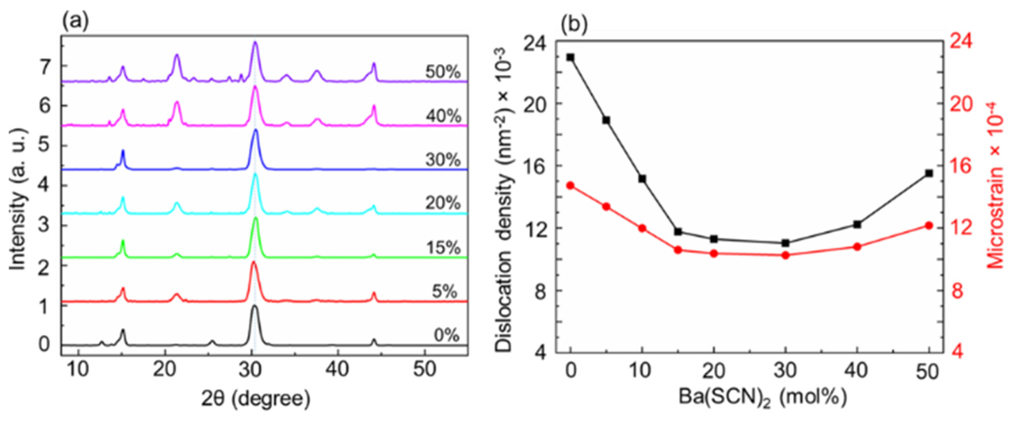
The crystalline structure of CsPbBr3 NCs with the addition of varying molar concentrations of Ba(SCN)2 (0–50%) is analyzed by XRD patterns, shown in Figure 2a. These patterns indicate that the main peaks are at ~15°, 21°, 26°, 30°, and 44°, which correspond to the (100), (110), (111), (200), and (220) diffraction planes of the cubic structure of CsPbBr3, respectively. An identical diffraction peak position observed despite varying concentrations of Ba(SCN)2 implies that the crystalline structure of the NCs is independent of the addition of Ba(SCN)2. A small peak was observed at about 12° for the parent CsPbBr3 NCs, indicating an incomplete transformation of PbBr2 into the CsPbBr3 structure. The peak corresponding to PbBr2 disappeared after the addition of Ba(SCN)2, showing the increased purity in the composition of the new compounds up to a doping concentration of 30%. This result indicates that the presence of barium is expected to limit the formation of metallic Pb from the resulting NCs, which act as non-radiative recombination centers [26]. Calculation of Goldschmidt’s tolerance and octahedral factors suggests that the addition of the guest elements Ba2+ and SCN is compatible with Pb2+ and Br. However, the addition affected crystal parameters, such as the crystallite size (L), dislocation density (), and microstrain (ϵ). L is calculated using the Scherrer equation [27]:
L = K λ β   C o s   θ
where K = 0.9 is the shape factor, is the full width at half maximum (FWHM) of the XRD peak, and θ is the diffraction angle. Then,
= n L 2
where n = 1 for minimum dislocation density. Using the Williamson–Hall equation, by definition,
ϵ = β 4   T a n θ
The values for , , and ϵ are summarized in Table S1, and the variations of and ϵ with Ba(SCN)2 are plotted in Figure 2b. We observed a variation of , confirming the presence of microstrain or inhomogeneous strain in the perovskite structure. The decrease in with the addition of Ba(SCN)2 suggests the enhancement of crystallinity. However, with a greater than 30% of addition, is slightly increased, which can be considered to be a critical dopant. The narrowing of the XRD peak width can be attributed to diminishing stacking faults and structural disorder [38]. This variation is further confirmed by the calculation of the dislocation density (Table S1) and crystallinity. The value of L is increased for 0–30% of Ba(SCN)2; however, further increasing the mol% of Ba(SCN)2 resulted in lower L due to the induced non-uniform strain [39]. It is noted that the microstrain is diminished when the mol% of Ba(SCN)2 is increased up to 30% and then slightly increased for the higher mol% of dopant. The induced microstrain influences the crystallinity of the sample. For higher mol% of Ba(SCN)2, the crystallinity falls off. The introduction of guest ions resulted in an enhanced crystallization due to its crucial role in favoring crystal growth by changing the growth surface energy [38,40]. Due to the chemical heterogeneity effect of thiocyanate ions, the introduction of thiocyanate-based salt leads to an increase in the Gibbs energy for nucleation owing to the change in surface energy, which further induces the difference in the crystallization process [41]. This is because the shift in nucleation rate brings a change in the growth kinematics of the NCs, which, in turn, leads to the variation in the morphology, and hence surface energy of NCs. The decrease in the microstrain indicates that the introduction of guest elements reduces the density of crystal defects (governing the non-radiative recombination), which is likely to improve the optoelectronic performance. Besides, depleting microstrain favors grain growth [38,42]. The sudden increase in microstrains with higher concentrations (>30%) of Ba(SCN)
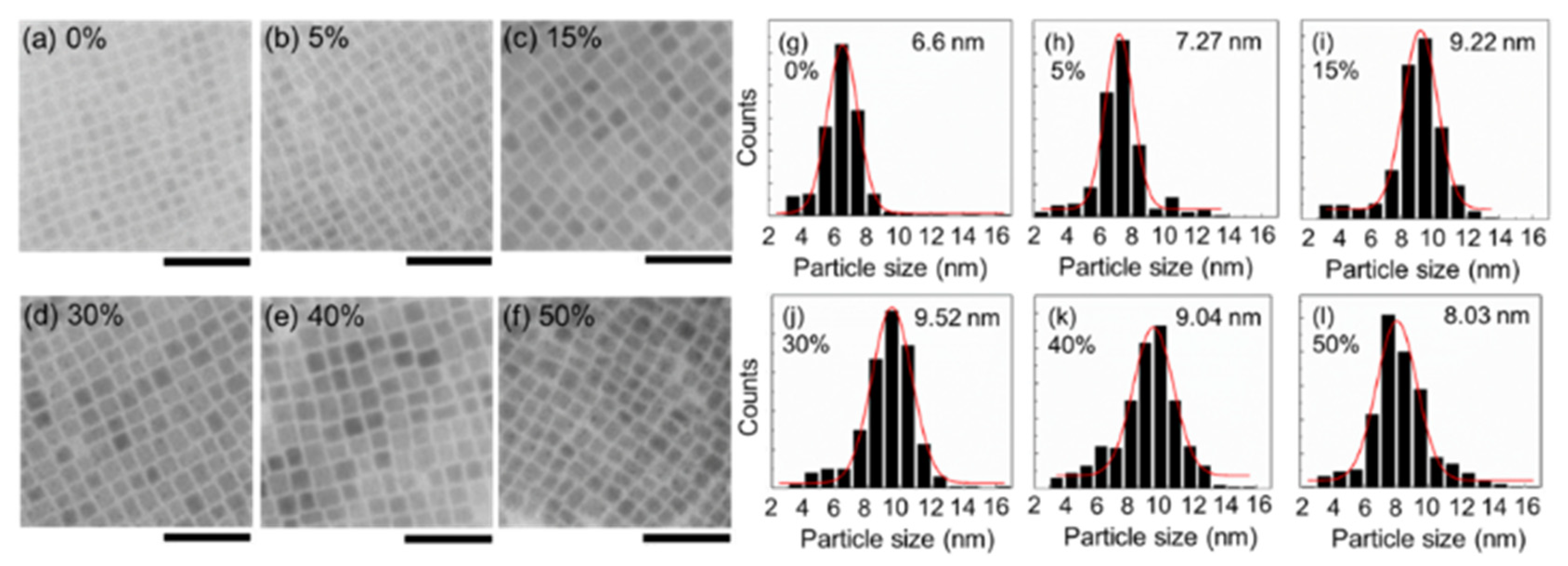
2 leads to the deterioration in crystallinity of the NCs and is prone to reduce the crystallite size. The morphology of the as-synthesized NCs is studied based on TEM images, as shown in Figure 3a–f, which demonstrate the impact of dopants on the nucleation and growth of NCs. The images exhibit a cubic shape of the NCs with a narrower size distribution. The morphology of the NCs remained identical even after the incorporation of Ba(SCN)2, with only changes in the average dimension. The average edge length of the NCs is settled in the range of 6.6–9.52 nm. A variation in particle size with different concentrations of Ba(SCN)2 is shown in Figure S1a. The histograms of the corresponding size distribution are shown in Figure 3g–l. An increase in the size of the cubes with the amount of Ba(SCN)2 up to 30% is observed, and particle size decreased with a higher concentration of Ba(SCN)2. Thus, we can say that particle size enhancement becomes saturated at 30% of Ba(SCN)2. This is due to increasing the crystallite size and reducing the microstrain and dislocation density for the lower percentage of dopant, which favors crystal growth [27]. However, due to increased non-uniform microstrains, crystal growth is lowered for higher percentages of addition, and a reduced particle size is observed. Further addition diminished the development of the NCs due to the strong bonding interaction between B-site cations and S and N. The variation in particle size exhibited a direct effect on the optical properties of the NCs.
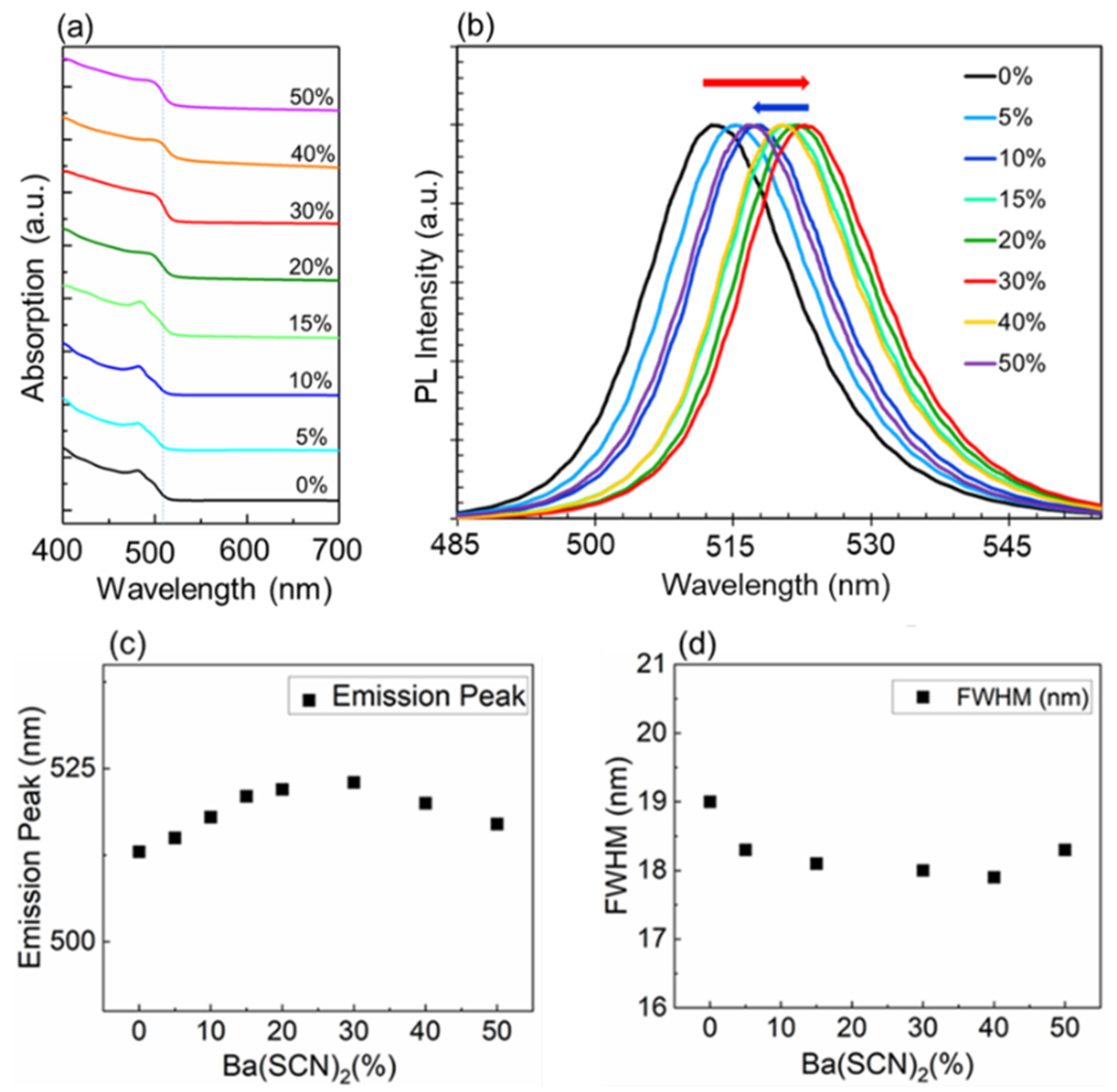
The optical properties of as-synthesized NCs are studied using absorption and PL emission spectra in Figure 4. The absorption onset (Figure 4a) is found to shift to longer wavelengths with the addition of Ba(SCN)2 and becomes saturated at 30% of Ba(SCN)2. Beyond this critical dopant, it is blue-shifted. The bandgap is calculated using Tauc Plot. The values are recorded in Table 1, and the variation of the bandgap with various concentrations of Ba(SCN)2 is shown in Figure S1b. For 0% of Ba(SCN)2, the bandgap is 2.450 eV; at 30%, it decreases to 2.413 eV; and at 50%, the bandgap increases to 2.418 eV. A similar trend is noticed in the PL emission peak position (Figure 4b), which is summarized in Table 1. A variation of the peak position with various mol% of Ba(SCN)2 is shown in Figure 4c. The corresponding PL emission peaks are 513 nm, 523 nm, and 517 nm, respectively, under the excitation wavelength of 365 nm. It should be noted that the fluctuation in optical properties is caused by variation in the size of the as-grown particles for different concentrations of Ba(SCN)2. It is generally accepted that the lead halide perovskites are defect-tolerant, due to the ionic nature of the material or the orbital composition of the energy bands [43]. This property is responsible for the optical transition after the addition of guest elements. In addition, the difference in the electronegativity of B-site and X-site elements plays some role in changing the energy gap and optical properties due to the orbital overlap [22,44]. The FWHM of the PL emission spectra of the samples is found to decrease after the addition of Ba(SCN)2, falling in the range of 19.07–18.07 nm. The variation of FWHM with the amount of Ba(SCN)2 added is shown in Figure 4d. The spectral purity of the light emission is demonstrated by the lowered value of FWHM of the PL emission. The PLQY of as-grown NCs is calculated (Figure S2) and compiled in Table 1. The PLQY is enhanced from 72% to 98% when the amount of dopant is increased from 0% to 50%, due to the combined effect produced by Ba2+ and SCN. As a result, surface defect states, such as dangling bonds, surface imperfections, etc., are eliminated, favoring the reduction of non-radiative decay and enhancement of PLQY of the NCs [38]. Xiang et al. also demonstrated that the addition of Ba2+ into the parent CsPbBr3 lattice effectively inhibits non-radiative recombination [26]. These results indicate that the addition of Ba(SCN)2 could help tune and enhance the optical properties of the host CsPbBr
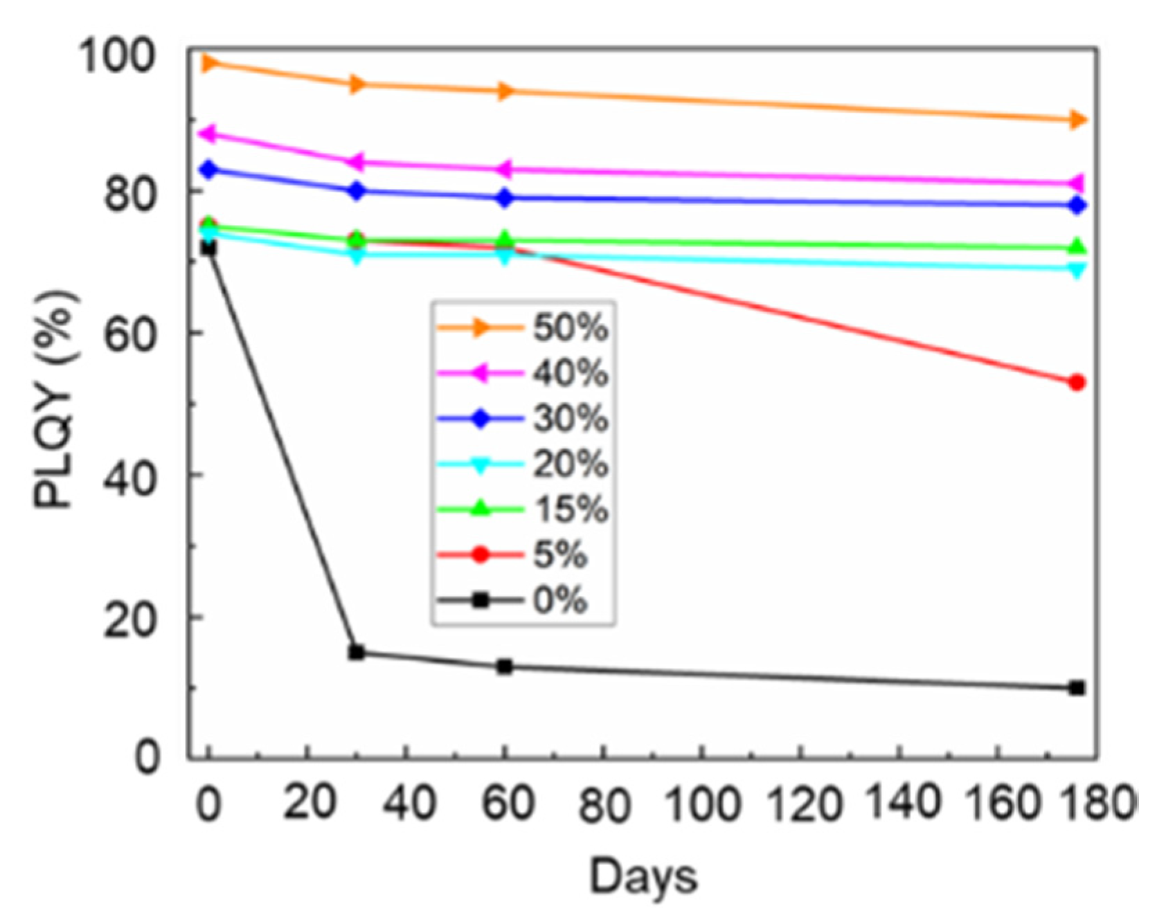
3 NCs. Time variations of PLQY of the as-prepared samples with different concentrations of Ba(SCN)2 are summarized in Table S2 and plotted in Figure 5. The samples with Ba(SCN)2 (>15%) retained the PLQY (>92% of the original value) even after prolonged exposure to an ambient atmosphere. However, the undoped sample retained very low PLQY (<13% of the PLQY of the fresh sample) and PL intensity. One hypothesis could be attributed to water molecules absorbed by pristine NCs, which may penetrate their structures, thereby deteriorating the colloidal integrity and degrading the luminous property. The durable performance and stability of the Ba(SCN)2-added samples in an ambient atmosphere could be ascribed to the passivation effect of Ba(SCN)2 which resulted in the reduction of defect concentrations. Furthermore, Ba(SCN)2 acts as a ligand that may inhibit the penetration of water into the core structure of the perovskite materials. The PL emission spectra of the fresh and aged samples for the various concentrations of Ba(SCN)2, indicating a blue shift in the peak position, are depicted in Figure S3. The displacement in the peak position suggests the photo-oxidation and photochemical degradation of the NCs, which was also demonstrated by the additional decrease in PLQY [45]. This shift is smaller with 50% of Ba(SCN)2, which demonstrates that the addition of 50% dopant is feasible to obtain more stable and higher-quality NCs. Furthermore, it is noted that the FWHM of the doped NCs has not significantly increased compared to the undoped samples (Figure S3) over a long period (+176 days). This suggests that the doped NCs maintain the purity of the color emission. For visualization, photographs of the colloidal solution of as-synthesized NCs (fresh and 176 days aged) under UV light are taken and shown in Figure S4. It is observed that all the fresh samples (Figure S4a) produced excellent luminous behavior. The samples without Ba(SCN)2 have seemingly degraded into an almost non-luminescent state after aging; however, the addition of Ba(SCN)2 stabilized the NCs (Figure S4b). The prolonged stability could be attributed to the protection of the NCs with defect reduction in the presence of Ba2+ and bonding interaction of Pb2+ with S and N, which is very strong due to the linear shape of SCN [30]. Thus, the prolonged luminous behavior of the Ba(SCN)2-doped samples can be promising in applications for device fabrication.
The normalized PL excitation spectra of CsPbBr3 NCs with the addition of varying molar concentrations of Ba(SCN)2 are shown in Figure S5. These spectra are measured by monitoring the corresponding peak emission wavelength. The excitation spectra are almost identical. The broadband excitation spectra extending from 270–480 nm indicates the favorability of the material to be used in a wide range of excitations. It is noted that the excitation spectra became continuous with an increasing amount of dopant. Spectra having a dual spectral band correspond to the charge-separated bandgap state at a higher wavelength and the charge transfer band at a lower wavelength [46]. The excitation range encompasses the emission range of UV/blue LED chips. This indicates that these types of particles can be applied in alliance with III-nitride-based UV/blue LED for the generation of white light via the photon down-conversion method. The excellent optical properties, such as narrow emission width, high PLQY, and wide range of excitation spectra, suggest that the as-prepared solution-processed NCs are promising alternatives to conventional and expensive phosphors for LED applications.
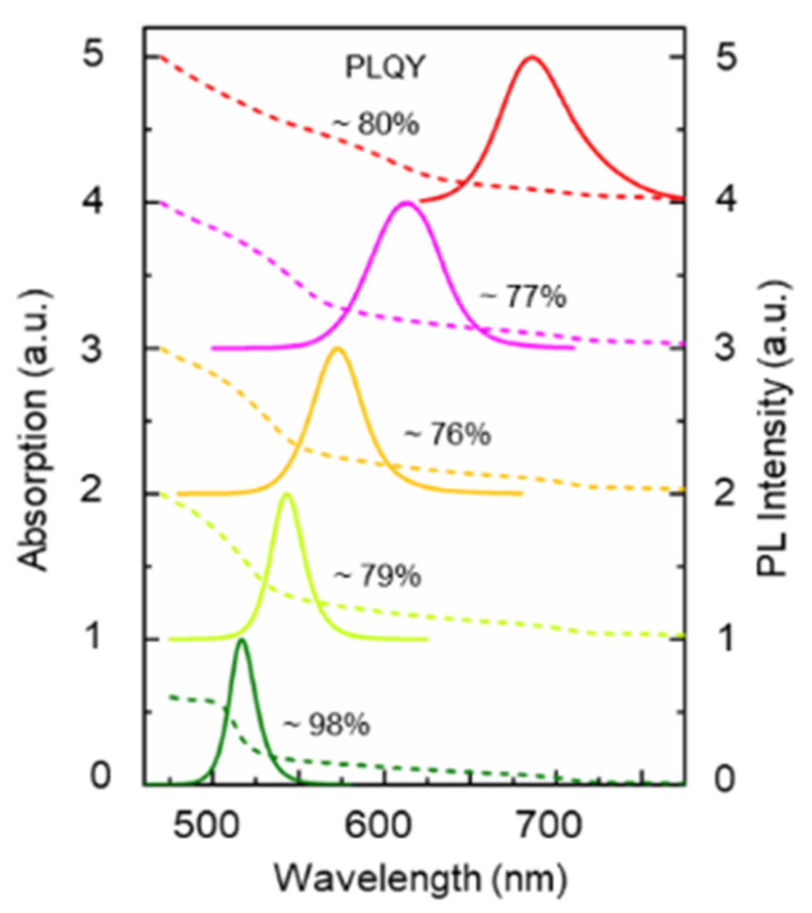
To explore the application of these new kinds of NCs in white LEDs, NCs having green-to-red tunable emission are synthesized by varying the proportionate amount of halides (Br/I) in CsPbX3 NCs with 50% of Ba(SCN)2, as shown in Figure 6. The dotted spectra denote absorption, and the solid spectra indicate normalized PL emission spectra. The bandgap is finely tuned from 2.416 eV to 1.86 eV by increasing the content of I. The emission peak is engineered across a significant portion of the visible spectral region (517–687 nm), with narrow FWHM (18–40 nm) and PLQY ≥ 76%. These properties of NCs are desirable for application in many lighting devices.
Furthermore, we found that the luminous property of as-fabricated perovskite NCs is excellent, including a narrow linewidth of emission spectra and a wide color gamut, indicating promising applications in white light emission. However, halide perovskites have an anion exchange reaction and instability issues when mixed and thus cannot be simply mixed to produce white light compared to Cd-based quantum dots [15,
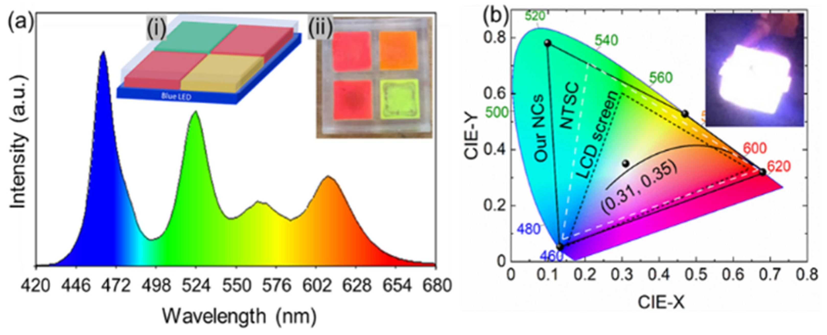
47]. On the other hand, when these NCs are directly coated onto blue/UV LED chips, the device experiences thermal instability because of the heat produced during the working cycle of the LED chips. Several studies have addressed these issues by using the remote phosphor technique of stacking glass plates containing different NCs as conversion layers over the blue/UV LED chips. In this configuration, the phosphors were exposed to less heat released from the chips due to the air barrier maintained between them. This non-contact configuration effectively eliminates the direct effect of heat on the phosphors without interfering with the LED junction. However, the multiple conversion layers over blue/UV LEDs suffer from reabsorption of light. For the first time, we fabricated a white LED using a 3D-printed single-color conversion layer utilizing a multipixel design to address these issues. The schematic diagram of the as-designed white LED is shown in the inset of Figure 7a(i). By using a clear UV-resin, we printed a 3D squared case with a multi-box design and dropped the desired amount of colloidal solution of different NCs into the individual boxes. Next, the samples were dried inside the vacuum oven at room temperature. The NCs were capped using epoxy resin to guard against deterioration from atmospheric moisture and air, as shown in the inset of Figure 7a(ii). This technique eliminates any anion-exchange reaction between the different halides, coffee-ring effect (the dispersing of NCs along the perimeter after drying, which normally occurs when spin-coating or when the colloidal solution of NCs is simply dropped on plain quartz/glass substrates), the direct heating effect on the phosphors from the LED chips, and reabsorption of light which commonly occurs in multi-layer conversion methods. It also excludes the cumbersome task of preparing multi-layers and stacking them on top of the blue/UV LEDs. We found that the 3D-printed multiplex conversion layer has a little detrimental effect on the luminescent property of the phosphors because of the excellent transparency of the UV resin. The white LED is fabricated based on the remote phosphor technique using a 3D-printed, transparent, multiplex-designed, single-color conversion layer. We used green (λ ~ 517 nm), yellow (λ ~ 572 nm), and red (λ ~ 615 nm) emitting NCs as different phosphors, which are pumped by the blue LED chips. The fabricated LED shows an emission peak of about 460 nm and runs at 3.97 mA and 7.50 V. The EL spectrum of the emitted white light is measured (Figure 7a) to analyze the color quality. Discrete peaks located at about 460 nm, 517 nm, 572 nm, and 615 nm are obtained, indicating the elimination of the anion exchange reaction between the different halides. The discrete peaks of the EL spectrum belonging to the blue LED, green-, yellow-, and red-emitting NCs, respectively, demonstrate a good combination of phosphors to obtain white light. Figure 7b represents the CIE (Commission Internationale de l’Eclairage) color system of the XY chromaticity diagram, used to compare the quality of the light source through mapping colors visible to the human eye in terms of hue and saturation. The area enclosed by the CIE diagram (smooth blue lines) represents the range of colors that human beings can see using naked eyes. The three triangles indicate the color gamut of the LCD TV screen (dotted black lines), the National Television Standards Committee’s (NTSC) TV screens (dotted white lines), and the as-synthesized NCs (solid black lines). The region within the color gamut demonstrates the capability of the color display per product, compatible with a color gamut. The color gamut of as-synthesized NCs (green, yellow, and red), including blue LEDs, representing a standard capable of displaying a wide range of colors, is larger than that of the NTSC standard and LCD TVs. A photograph of the as-fabricated white LED is shown in the inset of Figure 7b(ii), which produces a bright white light with a CCT of 6764 K, a CRI of 87, and an LER of 333 lm/W. This CCT is considered a cool white light. The high values of CRI and LER are due to the narrow linewidth of emission spectra of as-synthesized NCs. The high value of the CRI also indicates that the as-generated white light renders nearly perfect light, while the high LER points to the high energy efficacy of LEDs. The CIE coordinates of the white light we observed are (0.31, 0.35), as shown in Figure 7b (the center black point on the CIE diagram), and the value of Duv is 0.02, which indicates that the color coordinates of the light source lie in proximity to the Planckian locus (the center black curve on the CIE diagram). Thus, the light source is considered capable of emitting light comfortable to the human eye, even after prolonged exposure. Therefore, the as-fabricated device exhibits excellent color saturation, which is more desirable for general illuminations. These excellent properties of white light illustrate the likelihood of these compounds being used as alternatives to conventional rare-earth element-doped phosphors.
This development in perovskite NCs adds a new class of members to the family of colloidal metal halide NCs that can provide desired and stable optical features with high quantum yields even when exposed to air and moisture for five months. The as-synthesized materials appear to be a solid alternative to conventional rare-earth-doped phosphors, which will significantly increase studies related to next-generation WLEDs to achieve energy saving. Besides, the novel use of resin 3D-printing technology for designing LED components offers the ability to print stable and custom designs, enabling more accurate prints and limiting material waste. Thus, the substantial development of this printing technology could allow significant breakthroughs in reducing manufacturing costs and prompts toward commercialization. Resin-printing techniques with the primary goal of eliminating the phenomenon of light absorption in designing LEDs are still being developed and researched. Current challenges of obtaining highly transparent resin and design of compact structures for LED applications are prevalent issues to be solved. Besides, it is crucial that the integration of NCs with resin should impart desirable optical features of perovskite materials (such as high quantum yield) without much deterioration, or at least minimize the optical loss because of the quenching and agglomeration effect. In the future, we can work on optimizing WLED structures based on a 3D-printed color conversion layer by studying the operation stability of the device structure.

4. Conclusions

In summary, we added barium thiocyanate [Ba(SCN)2] as a dopant to the all-inorganic CsPbX3 perovskites and studied the function of new components to the host NCs. A variation in crystal parameters was observed with almost identical phase and lattice dimensions, which suggests that the addition of the guest components resided in the surface of the parent NCs. This variation yielded a change in particle size with the same morphology, which resulted in the alternation of the PL emission peak position and bandgap energy. The PLQY near unity (98%) was also achieved. The surface of the host NCs became passivated with the addition of dopants while removing excessive amounts of Pb2+ resulted in an enhanced PLQY. Moreover, for the first time, we reported on a new technique for fabricating white LEDs using a 3D-printed multipixel structure and investigated the performance of as-synthesized compounds. A qualitative white light was obtained with a CCT of 6764 K, a CRI of 87, and an LER of 333 lm/W. These values suggest excellent color characteristics for practical lighting applications. This study provides an efficient approach toward metal halide perovskites-based optoelectronic devices for future lighting technology.

Supplementary Materials

The following are available online at https://www.mdpi.com/article/10.3390/photonics8060209/s1; Table S1: FWHM of diffraction peak (β), dislocation density (ẟ), and micro-strain (ϵ) of CsPbBr3 NCs with the addition of different molar concentrations of Ba(SCN)2; Figure S1: The variation of (a) particle size and (b) band gap of CsPbBr3 NCs with the addition of different molar concentrations of Ba(SCN)2; Figure S2: Scattering and emission spectra without and with samples. The absolute PLQY is calculated using the formula demonstrated in the inset of the Figure. Sref and Eref are areas covered by scattering and emission spectra of the reference liquid on the X-axis, and Ssam and Esam are areas covered by scattering and emission spectra of the sample in the reference liquid; Table S2: Time variation of PLQY of CsPbBr3 NCs with the addition of different molar concentrations of Ba(SCN)2; Figure S3: Normalized PL emission spectra of fresh and aged (+176 days in an ambient atmosphere) CsPbBr3 NCs with different molar concentrations of Ba(SCN)2 as indicated. The graph illustrates a blue shift in the PL emission peak position with an increasing storage time; Figure S4: Digital photographs (under the UV light) of the colloidal solution of CsPbBr3 NCs at different molar concentrations of Ba(SCN)2. (a) Fresh samples and (b) 176 days aged samples in an ambient atmosphere; Figure S5: Normalized excitation spectra of CsPbBr3 NCs at a different molar concentration of Ba(SCN)2.

Author Contributions

Conceptualization, H.Z. and P.Z.; data curation, G.C.A. and S.T.; formal analysis, G.C.A., S.T., H.Z. and P.Z.; funding acquisition, P.Z.; investigation, G.C.A. and S.T.; methodology, G.C.A., S.T., H.Z. and P.Z.; project administration, P.Z.; resources, H.Z. and P.Z.; supervision, P.Z.; writing—original draft, G.C.A. and S.T.; writing—review and editing, S.T., Y.Y., H.Z. and P.Z., G.C.A. and S.T. have equal contributions to the work. All authors have read and agreed to the published version of the manuscript.

Funding

This research was funded by the National Science Foundation, 1945558.

Data Availability Statement

The data used to support the findings of this study are included within the article and Supplementary Material.

Acknowledgments

The authors would like to acknowledge Alexei Grigoriev’s help with XRD measurements, Parameswar Harikumar’s help with absorption measurements, and Richard Portman’s help with TEM measurements.

Conflicts of Interest

The authors declare no conflict of interest. The funders had no role in the design of the study; in the collection, analyses, or interpretation of data; in the writing of the manuscript, or in the decision to publish the results.

References

  1. Veldhuis, S.A.; Boix, P.P.; Yantara, N.; Li, M.; Sum, T.C.; Mathews, N.; Mhaisalkar, S.G. Perovskite materials for light-emitting diodes and lasers. Adv. Mater. 2016, 28, 6804–6834. [Google Scholar] [CrossRef]
  2. Yang, S.; Fu, W.; Zhang, Z.; Chen, H.; Li, C.-Z. Recent advances in perovskite solar cells: Efficiency, stability and lead-free perovskite. J. Mater. Chem. A 2017, 5, 11462–11482. [Google Scholar] [CrossRef]
  3. Chin, X.Y.; Cortecchia, D.; Yin, J.; Bruno, A.; Soci, C. Lead iodide perovskite light-emitting field-effect transistor. Nat. Commun. 2015, 6, 7383. [Google Scholar] [CrossRef] [PubMed]
  4. Pammi, S.V.N.; Maddaka, R.; Tran, V.-D.; Eom, J.-H.; Pecunia, V.; Majumder, S.; Kim, M.-D.; Yoon, S.G. CVD-deposited hybrid lead halide perovskite films for high-responsivity, self-powered photodetectors with enhanced photo stability under ambient conditions. Nano Energy 2020, 74, 104872. [Google Scholar] [CrossRef]
  5. Maksym, V.; Kovalenko, L.P.; Bodnarchuk, M.I. Properties and potential optoelectronic applications of lead halide perovskite nanocrystals. Science 2017, 358, 745–750. [Google Scholar]
  6. Chen, Y.; Liu, Y.; Hong, M. Cation-doping matters in caesium lead halide perovskite nanocrystals: From physicochemical fundamentals to optoelectronic applications. Nanoscale 2020, 12, 12228–12248. [Google Scholar] [CrossRef]
  7. Zhu, H.; Cai, T.; Que, M.; Song, J.-P.; Rubenstein, B.M.; Wang, Z.; Chen, O. Pressure-induced phase transformation and band-gap engineering of formamidinium lead Iodide perovskite nanocrystals. J. Phys. Chem. Lett. 2018, 9, 4199–4205. [Google Scholar] [CrossRef] [PubMed]
  8. Protesescu, L.; Yakunin, S.; Bodnarchuk, M.I.; Krieg, F.; Caputo, R.; Hendon, C.H.; Yang, R.X.; Walsh, A.; Kovalenko, M.V. Nanocrystals of cesium lead halide perovskites (CsPbX3, X = Cl, Br, and I): Novel optoelectronic materials showing bright Emission with wide color gamut. Nano Lett. 2015, 15, 3692–3696. [Google Scholar] [CrossRef]
  9. Tong, Y.; Bladt, E.; Ayguler, M.F.; Manzi, A.; Milowska, K.Z.; Hintermayr, V.A.; Docampo, P.; Bals, S.; Urban, A.S.; Polavarapu, L.; et al. Highly luminescent cesium lead halide perovskite nanocrystals with tunable composition and thickness by ultrasonication. Angew. Chem. Int. Ed. 2016, 55, 13887–13892. [Google Scholar] [CrossRef]
  10. Adhikari, G.C.; Zhu, H.; Vargas, P.A.; Zhu, P. UV-Green emission from organolead bromide perovskite nanocrystals. J. Phys. Chem. C 2018, 122, 15041–15046. [Google Scholar] [CrossRef]
  11. Zhang, L.; Zeng, Q.; Wang, K. Pressure-induced structural and optical properties of inorganic halide perovskite CsPbBr3. J. Phys. Chem. Lett. 2017, 8, 3752–3758. [Google Scholar] [CrossRef]
  12. Nagaoka, Y.; Hills-Kimball, K.; Tan, R.; Li, R.; Wang, Z.; Chen, O. Nanocube superlattices of cesium lead bromide perovskites and pressure-induced phase transformations at atomic and mesoscale levels. Adv. Mater. 2017, 29, 1606666. [Google Scholar] [CrossRef]
  13. Polavarapu, L.; Nickel, B.; Feldmann, J.; Urban, A.S. Advances in quantum-confined perovskite nanocrystals for optoelectronics. Adv. Energy Mater. 2017, 7, 1700267. [Google Scholar] [CrossRef]
  14. Guner, T.; Demir, M.M. A review on halide perovskites as color conversion layers in white light emitting diode applications. Phys. Status Solidi A 2018, 215, 1800120. [Google Scholar] [CrossRef]
  15. Zhu, P.; Zhu, H.; Adhikari, G.C.; Thapa, S. Spectral optimization of white light from hybrid metal halide perovskites. OSA Contin. 2019, 2, 1880–1888. [Google Scholar] [CrossRef]
  16. Thapa, S.; Adhikari, G.C.; Zhu, H.; Grigoriev, A.; Zhu, P. Zn-alloyed all-Inorganic halide perovskite-based white light-emitting diodes with superior color quality. Sci. Rep. 2019, 9, 18636. [Google Scholar] [CrossRef] [PubMed]
  17. Kamat, P.V.; Bisquert, J.; Buriak, J. Lead-free perovskite solar cells. ACS Energy Lett. 2017, 2, 904–905. [Google Scholar] [CrossRef]
  18. Zhang, L.; Liu, C.; Wang, L.; Liu, C.; Wang, K.; Zou, B. Pressure-induced emission enhancement, band-gap narrowing, and metallization of halide perovskite Cs3Bi2I9. Angew. Chem. Int. Ed. 2018, 57, 11213–11217. [Google Scholar] [CrossRef] [PubMed]
  19. Swarnkar, A.; Mir, W.J.; Nag, A. Can B-site doping or alloying improve thermal- and phase-stability of all-inorganic CsPbX3 (X = Cl, Br, I) perovskites? ACS Energy Lett. 2018, 3, 286–289. [Google Scholar] [CrossRef]
  20. Zhou, Y.; Chen, J.; Bakr, O.M.; Sun, H.-T. Metal-doped lead halide perovskites: Synthesis, properties, and optoelectronic applications. Chem. Mater. 2018, 30, 6589–6613. [Google Scholar] [CrossRef]
  21. Ke, W.; Kanatzidis, M.G. Prospects for low-toxicity lead-free perovskite solar cells. Nat. Commun. 2019, 10, 965. [Google Scholar] [CrossRef]
  22. Jacobsson, T.J.; Pazoki, M.; Hagfeldt, A.; Edvinsson, T. Goldschmidt’s rules and strontium replacement in lead halogen perovskite solar cells: Theory and preliminary experiments on CH3NH3SrI3. J. Phys. Chem. C 2015, 119, 25673–25683. [Google Scholar] [CrossRef]
  23. Adhikari, G.C.; Thapa, S.; Zhu, H.; Zhu, P. Mg2+-alloyed all-inorganic halide perovskites for white light-emitting diodes by 3D-printing method. Adv. Opt. Mater. 2019, 7, 1900916. [Google Scholar] [CrossRef]
  24. Mir, W.J.; Sheikh, T.; Arfin, H.; Xia, Z.; Nag, A. Lanthanide doping in metal halide perovskite nanocrystals: Spectral shifting, quantum cutting and optoelectronic applications. NPG Asia Mater. 2020, 12. [Google Scholar] [CrossRef]
  25. Liu, W.; Lin, Q.; Li, H.; Wu, K.; Robel, I.; Pietryga, J.M.; Klimov, V.I. Mn2+-doped lead halide perovskite nanocrystals with dual-color emission controlled by halide content. J. Am. Chem. Soc. 2016, 138, 14954–14961. [Google Scholar] [CrossRef] [PubMed]
  26. Xiang, W.; Wang, Z.; Kubicki, D.J.; Wang, X.; Tress, W.; Luo, J.; Zhang, J.; Hofstetter, A.; Zhang, L.; Emsley, L.; et al. Ba-induced phase segregation and band gap reduction in mixed-halide inorganic perovskite solar cells. Nat. Commun. 2019, 10, 4686. [Google Scholar] [CrossRef] [PubMed]
  27. Bahadur, J.; Ghahremani, A.H.; Gupta, S.; Druffel, T.; Sunkara, M.K.; Pal, K. Enhanced moisture stability of MAPbI3 perovskite solar cells through Barium doping. Sol. Energy 2019, 190, 396–404. [Google Scholar] [CrossRef]
  28. Chan, S.-H.; Wu, M.-C.; Lee, K.-M.; Chen, W.-C.; Lin, T.-H.; Su, W.-F. Enhancing perovskite solar cell performance and stability by doping barium in methylammonium lead halide. J. Mater. Chem. A 2017, 5, 18044–18052. [Google Scholar] [CrossRef]
  29. Walker, B.; Kim, G.H.; Kim, J.Y. Pseudohalides in lead-based perovskite semiconductors. Adv. Mater. 2019, 31, 1807029. [Google Scholar] [CrossRef]
  30. Jiang, Q.R.D.; Gong, J.; Piacentino, E.L.; Zheng, C.; Xu, T. Pseudohalide-induced moisture tolerance in perovskite CH3NH3Pb(SCN)2I thin films. Angew. Chem. Int. Ed. Engl. 2015, 54, 7617–7620. [Google Scholar] [CrossRef]
  31. Koscher, B.A.; Swabeck, J.K.; Bronstein, N.D.; Alivisatos, A.P. Essentially trap-free CsPbBr3 colloidal nanocrystals by postsynthetic thiocyanate surface treatment. J. Am. Chem. Soc. 2017, 139, 6566–6569. [Google Scholar] [CrossRef]
  32. Thapa, S.; Adhikari, G.C.; Zhu, H.; Zhu, P. Scalable synthesis of highly luminescent and stable thiocyanate based CsPbX3 perovskite nanocrystals for efficient white light-emitting diodes. J. Alloys Compd. 2021, 860, 158501. [Google Scholar] [CrossRef]
  33. Chen, F.; Boopathi, K.M.; Imran, M.; Lauciello, S.; Salerno, M. Thiocyanate-treated perovskite-nanocrystal-based Light-emitting diodes with insight in efficiency roll-off. Materials 2020, 13, 367. [Google Scholar] [CrossRef] [PubMed]
  34. Han, T.-H.; Lee, J.-W.; Choi, C.; Tan, S.; Lee, C.; Zhao, Y.; Dai, Z.; De Marco, N.; Lee, S.-J.; Bae, S.-H.; et al. Perovskite-polymer composite cross-linker approach for highly-stable and efficient perovskite solar cells. Nat. Commun. 2019, 10, 520. [Google Scholar] [CrossRef] [PubMed]
  35. Xin, Y.; Zhao, H.; Zhang, J. Highly stable and luminescent perovskite–polymer composites from a convenient and universal strategy. ACS Appl. Mater. Interfaces 2018, 10, 4971–4980. [Google Scholar] [CrossRef]
  36. Adhikari, G.C.; Thapa, S.; Zhu, H.; Zhu, P. UV resin enhanced stability of metal halide perovskite nanocrystals for white light-emitting diodes. ACS Appl. Electron. Mater. 2019, 2, 35–40. [Google Scholar] [CrossRef]
  37. Zuo, L.; Guo, H.; de Quilettes, D.W.; Jariwala, S.; Marco, N.D.; Dong, S.; DeBlock, R.; Ginger, D.S.; Dunn, B.; Wang, M.; et al. Polymer-modified halide perovskite films for efficient and stable planar heterojunction solar cells. Sci. Adv. 2017, 3, e1700106. [Google Scholar] [CrossRef]
  38. Wang, J.T.-W.; Wang, Z.; Pathak, S.; Zhang, W.; de Quilettes, D.W.; Wisnivesky-Rocca-Rivarola, F.; Huang, J.; Nayak, P.K.; Patel, J.B.; Mohd Yusof, H.A.; et al. Efficient perovskite solar cells by metal ion doping. Energy Environ. Sci. 2016, 9, 2892–2901. [Google Scholar] [CrossRef]
  39. Wu, M.-C.; Chen, W.-C.; Chan, S.-H.; Su, W.-F. The effect of strontium and barium doping on perovskite-structured energy materials for photovoltaic applications. Appl. Surf. Sci. 2018, 429, 9–15. [Google Scholar] [CrossRef]
  40. Robinson, I.; Harder, R. Coherent X-ray diffraction imaging of strain at the nanoscale. Nat. Mater. 2009, 8, 291–298. [Google Scholar] [CrossRef] [PubMed]
  41. Kim, M.K.; Jeon, T.; Park, H.I.; Lee, J.M.; Nam, S.A.; Kim, S.O. Effective control of crystal grain size in CH3NH3PbI3 perovskite solar cells with a pseudohalide Pb(SCN)2 additive. CrystEngComm 2016, 18, 6090–6095. [Google Scholar] [CrossRef]
  42. Subhani, W.S.; Wang, K.; Du, M.; Liu, S.F. Goldschmidt-rule-deviated perovskite CsPbIBr2 by barium substitution for efficient solar cells. Nano Energy 2019, 61, 165–172. [Google Scholar] [CrossRef]
  43. ten Brinck, S.; Zaccaria, F.; Infante, I. Defects in lead halide perovskite nanocrystals: Analogies and (many) differences with the bulk. ACS Energy Lett. 2019, 4, 2739–2747. [Google Scholar] [CrossRef]
  44. Chen, Q.-Y.; Huang, Y.; Huang, P.-R.; Ma, T.; Cao, C.; He, Y. Electronegativity explanation on the efficiency-enhancing mechanism of the hybrid inorganic-organic perovskite ABX3 from first-principles study. Chin. Phys. B 2016, 25, 027104. [Google Scholar] [CrossRef]
  45. Raja, S.N.; Bekenstein, Y.; Koc, M.A.; Fischer, S.; Zhang, D.; Lin, L.; Ritchie, R.O.; Yang, P.; Alivisatos, A.P. Encapsulation of perovskite nanocrystals into macroscale polymer matrices: Enhanced stability and polarization. ACS Appl. Mater. Interfaces 2016, 8, 35523–35533. [Google Scholar] [CrossRef] [PubMed]
  46. Stamplecoskie, K.G.; Manser, J.S.; Kamat, P.V. Dual nature of the excited state in organic–inorganic lead halide perovskites. Energy Environ. Sci. 2015, 8, 208–215. [Google Scholar] [CrossRef]
  47. Pathak, S.; Sakai, N.; Wisnivesky Rocca Rivarola, F.; Stranks, S.D.; Liu, J.; Eperon, G.E.; Ducati, C.; Wojciechowski, K.; Griffiths, J.T.; Haghighirad, A.A.; et al. Perovskite crystals for tunable white light emission. Chem. Mater. 2015, 27, 8066–8075. [Google Scholar] [CrossRef]
Figure 1. Schematic illustration of synthesis of CsPbX3 NCs added with Ba(SCN)2 and their applications in WLEDs.
Photonics 08 00209 g001
Figure 2. (a) The normalized XRD patterns and (b) the variation of dislocation density and microstrain of CsPbBr3 NCs with the addition of different molar concentrations of Ba(SCN)2. The graph illustrates that the microstrain and the dislocation density decrease with an increasing content of dopants up to a critical doping concentration but increase beyond that doping content.
Photonics 08 00209 g002
Figure 3. (af) TEM images (scale bar set to 50 nm) of CsPbBr3 NCs with the addition of different molar concentrations of Ba(SCN)2. (gl) Histogram of the corresponding sample showing the size distribution of the particles. The statistical charts indicate that the size of the particle increases up to a critical dopant content and decreases thereafter.
Photonics 08 00209 g003
Figure 4. (a) Absorption spectra, (b) normalized PL emission spectra, (c) variation of PL emission peak wavelength, and (d) variation of PL FWHM of CsPbBr3 NCs with the addition of different molar concentrations of Ba(SCN)2. The absorption and the corresponding PL emission peak first exhibit the red-shift in the peak position up to a critical doping concentration and a blue-shift thereafter.
Photonics 08 00209 g004
Figure 5. The time variation PLQY of CsPbBr3 NCs with the addition of different molar concentration of Ba(SCN)2 as indicated. The PLQY of undoped NCs decreases rapidly within three weeks, whereas that of the doped NCs remains almost constant over a period of time, confirming the improved stability of doped NCs.
Photonics 08 00209 g005
Figure 6. The absorption spectra (dotted lines) and PL emission spectra (solid lines) of CsPbX3 NCs with 50% of Ba(SCN)2. The graph represents the decreasing ratio of Br to I results in the red-shift in the PL emission peak and the corresponding absorption peak position, respectively.
Photonics 08 00209 g006
Figure 7. (a) EL spectrum of white light. Inset: (i) schematic device structure of WLED with a 3D- printed multiplex color conversion layer stacked above the blue LED and (ii) picture of 3D-printed multiplex structure filled with different color emitting NCs. (b) CIE diagram provided with CIE color coordinates compares the color gamut of LCD screen and NTSC to the light emitted from as-synthesized perovskite NCs. Black data points on the edge and center correspond to the emission from as-synthesized NCs and device, respectively. Inset is the picture of the emitted white light from the device.
Photonics 08 00209 g007
Table 1. Bandgap, PL emission peak position, FWHM, and PLQY of CsPbBr3 NCs with the addition of different molar concentration of Ba(SCN)2.
Ba(SCN)2 (%)Bandgap (eV)PL Peak (nm)FWHM (nm)PLQY (%)
02.45051319.0772
52.44751518.6875
152.41652118.1775
202.41552218.1074
302.41452318.1283
402.41552118.0788
502.41651718.3098
Publisher’s Note: MDPI stays neutral with regard to jurisdictional claims in published maps and institutional affiliations.

