Review

Perspectives on UVC LED: Its Progress and Application

1
Department of Photonics & Graduate Institute of Electro-Optical Engineering, College of Electrical and Computer Engineering, National Chiao Tung University, Hsinchu 30010, Taiwan
2
Department of Photonics & Graduate Institute of Electro-Optical Engineering, College of Electrical and Computer Engineering, National Yang Ming Chiao Tung University, Hsinchu 30010, Taiwan
3
Fujian Engineering Research Center for Solid-State Lighting, School of Electronic Science and Engineering, Xiamen University, Xiamen 361005, China
4
Picosun China Co. Ltd., Suzhou 215000, China
5
Hon Hai Semiconductor Research Center, New Taipei City 23678, Taiwan
*
Author to whom correspondence should be addressed.
These authors contributed equally to this work.
Photonics 2021, 8(6), 196; https://doi.org/10.3390/photonics8060196
Submission received: 12 April 2021 / Revised: 25 May 2021 / Accepted: 28 May 2021 / Published: 31 May 2021
(This article belongs to the Special Issue Wide Bandgap Semiconductor Photonic Devices)

Abstract

:
High-quality epitaxial layers are directly related to internal quantum efficiency. The methods used to design such epitaxial layers are reviewed in this article. The ultraviolet C (UVC) light-emitting diode (LED) epitaxial layer structure exhibits electron leakage; therefore, many research groups have proposed the design of blocking layers and carrier transportation to generate high electron–hole recombination rates. This also aids in increasing the internal quantum efficiency. The cap layer, p-GaN, exhibits high absorption in deep UV radiation; thus, a small thickness is usually chosen. Flip chip design is more popular for such devices in the UV band, and the main factors for consideration are light extraction and heat transportation. However, the choice of encapsulation materials is important, because unsuitable encapsulation materials will be degraded by ultraviolet light irradiation. A suitable package design can account for light extraction and heat transportation. Finally, an atomic layer deposition Al2O3 film has been proposed as a mesa passivation layer. It can provide a low reverse current leakage. Moreover, it can help increase the quantum efficiency, enhance the moisture resistance, and improve reliability. UVC LED applications can be used in sterilization, water purification, air purification, and medical and military fields.

1. Background

Since the invention of the first nitride light-emitting diode (LED) by Pankove et al. in 1972 [1], the development of nitride LEDs was quite rapid. The most commonly used materials for this purpose have been group III nitrides, which result in LEDs with wide direct energy gaps that range from the infrared to ultraviolet bands. In 1998, Han et al. published the first report on an ultraviolet (UV) LED with an emission wavelength shorter than 360 nm [2]. Since then, UV LED technology has undergone significant development. One category operates in the deep UV (DUV) region, covering a wide range of applications that include air purifiers, water purifiers, disinfection and sterilization, polymer curing, and biomedical testing. With the rising international awareness of environmental protection, the International Minamata Convention in 2013 also pushed the development of the high efficiency DUV LED, which is an interesting replacement for low-pressure mercury lamps. Another feature of DUV-LEDs is that the light-emitting band can be modified through the adjustment of the epitaxial structure. This feature enables DUV-LEDs to be used in several fields of application. However, organic compounds can also emit UVC light. Most organic compounds are transparent to the relatively high-energy radiation that constitutes the ultraviolet (200–400 nm) and visible (400–700 nm) portion of the electromagnetic spectrum; thus, they appear colorless in solution [3].
In the electromagnetic spectrum, the wavelength of UV radiation is between the wavelengths of light and X-rays, covering 100 to 400 nm (12.4–3.1 eV). This wavelength range can be further subdivided into four bands, namely, long-wave ultraviolet UVA (315–400 nm), medium-wave ultraviolet UVB (280–315 nm), short-wave ultraviolet UVC (200–280 nm), and vacuum ultraviolet (100–200 nm). UVA serves as the primary light source in the curing of UV glue, light therapy, air purification, and 3D printing. On the other hand, UVB and UVC bands correspond to the peaks of the absorption spectra of DNA and RNA, enabling these UV bands to eliminate a large number of virus sources. This capability is especially important because of the increasing demand for water purification due to the scarcity of clean water resources. In particular, UVC has considerable development potential for medical applications such as purification cycle processing and sterilization. However, it may cause skin cancer under excessive exposure.
Most traditional UVC radiation sources use mercury lamps to produce shorter-wavelength UV radiation. The mercury vapor discharge is combined with different filters to produce bands with different light-emitting wavelengths. The most commonly used UVC radiation band is obtained from a low-pressure mercury lamp. The ignited vapor pressure is less than 1 atm, and the main radiation wavelength is 253.7 nm. In daily life, the lamp is used mostly for sterilization and disinfection; however, mercury is hazardous and is easily absorbed by the skin, respiratory tract, and digestive tract of organisms. It accumulates in organisms, and with biomagnification, the final content in the human body is quite high and thus may be fatal. Therefore, the United Nations passed the Minamata Convention and officially announced a total ban on the production of mercury-containing products after 2020. This also means that it is necessary to search for new objects to replace mercury lamps as ultraviolet light sources. Among them, DUV-LEDs are the most highly anticipated devices. Table 1 presents a summary of the applications of UVA, UVB, and UVC LEDs.
In this article, we will present an overview of the state of the art of UVC LED characteristics. Meanwhile, the future potential of UVC LEDs and the key parameters that affect the performance of UV emitters will be discussed.

2. Working Principle and Limitations of UVC LED

According to the UV Market report, the market of UVC grew from $20 million in 2008 to $100 million in 2015; then, it was $144 million in 2019. In addition, it supposed that the market of UVC LED would increase to $991 million in 2023 [5]. UVC LEDs have gradually entered the stage of commercial mass production. However, compared to the mature technology of blue LEDs, UVC LEDs have three main technical bottlenecks: low external quantum efficiency (EQE) of the chip, aging of the packaging material, and thermal management issues.

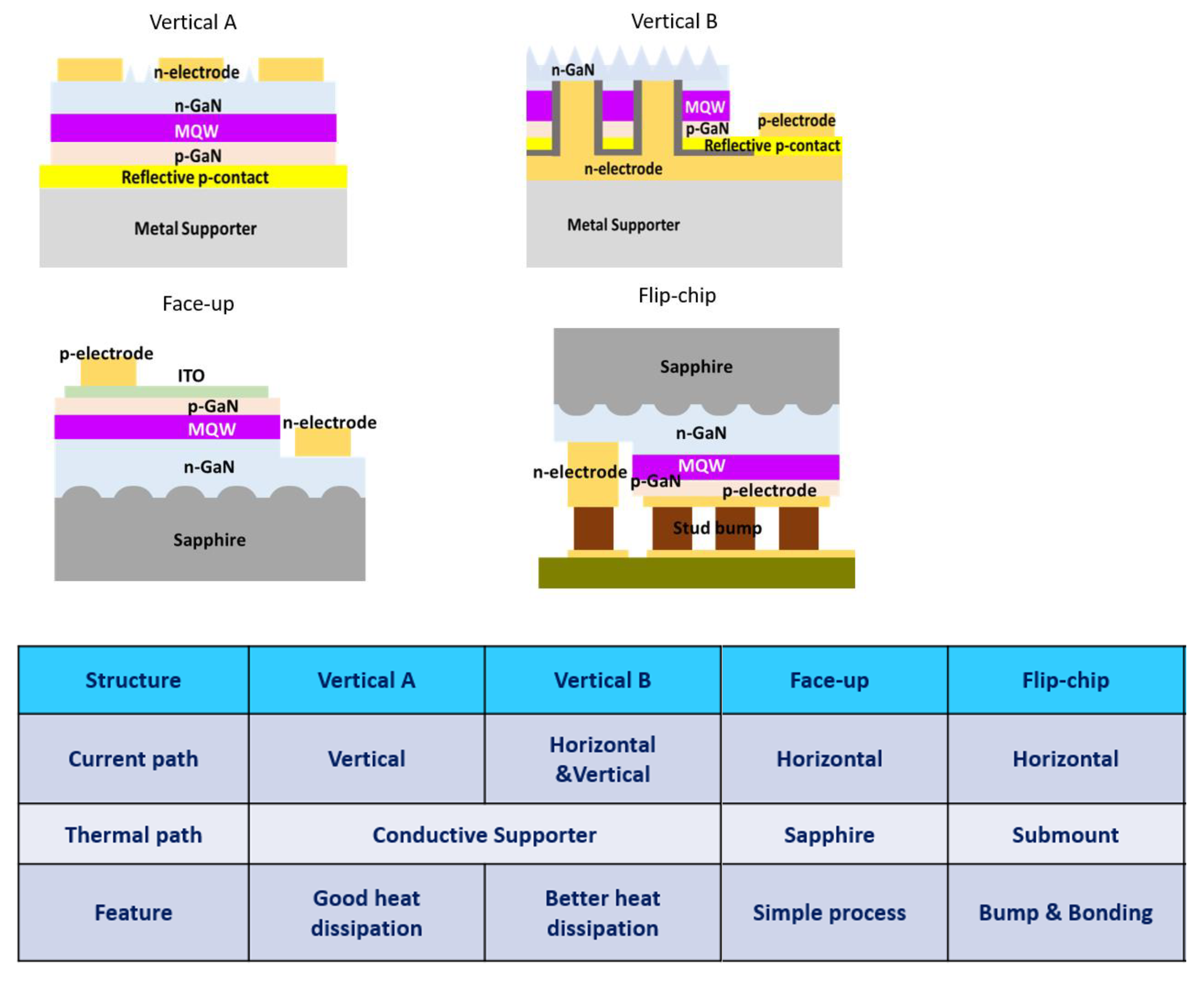
2.1. Introduction to UVC LED Devices

The bandgap of GaN and AlN are 3.4 and 6.2 eV, respectively. As the composition changes, the bandgap of AlGaN can range from 3.4 to 6.2 eV, which means that the material of AlGaN is very suitable for the fabrication of UVC LED devices [6]. An LED is a semiconductor light-emitting device based on a pn junction. The p-type and n-type layers are used to inject holes and electrons into the active region between them. Based on the device fabrication, we can separate UV LED chips into three types of device structures, namely, face up, flip-chip, and vertical type, as shown in Figure 1. The vertical type is more complicated in terms of fabrication: the wafer must first be mounted on a conductive support, followed by a top-side process, and then, the removal of the sapphire substrate. Although this set-up can result in good heat dissipation, the vertical design costs about three times as much as the other two types. By contrast, the fabrication process of the face-up chip is simple but does not lead to efficient light extraction and good quantum efficiency because of the p-metal shading part of the light and a worse current path. Therefore, the most commonly used UVC LED typically has a flip-chip structure; i.e., a substrate leads light at the top, whereas an electrode is connected to a circuit below. This structure can achieve better heat dissipation.
However, low EQE remains a challenge for UVC LED. Figure 2 shows the EQEs of UV LEDs in the spectral range between 200 and 400 nm [7]. A noticeably large drop in EQE occurs for wavelengths shorter than 365 nm, which marks the transition from InGaN- to AlGaN-based LED technologies, whereas near-UV LEDs exhibit performance levels close to those of blue LEDs with EQEs ranging from 46 to 76% [8]. By contrast, for UV LEDs with wavelengths near 275 nm, peak EQEs of 20% have been reported [9]. However, although sharp drops in EQE at wavelengths shorter than 250 nm and significant dips across the UVB band continue to be observed, the root causes of rapidly dropping emission power levels and EQEs with decreasing emission wavelengths remain unclear. Typically, this behavior is attributed to several mechanisms, mainly to a reduced internal quantum efficiency (IQE), reduced carrier injection efficiency (CIE), and reduced light extraction efficiency (LEE) [10,11] due to changes in the optical polarization of emitted light, from transverse electric (TE) to transverse magnetic (TM), at emission wavelengths of approximately 240 nm [12,13] for fully strained MQWs on AlN. On the other hand, in discussions on these mechanisms, the reabsorption of emitted light within the n-side of the LED heterostructure is typically not considered [14].

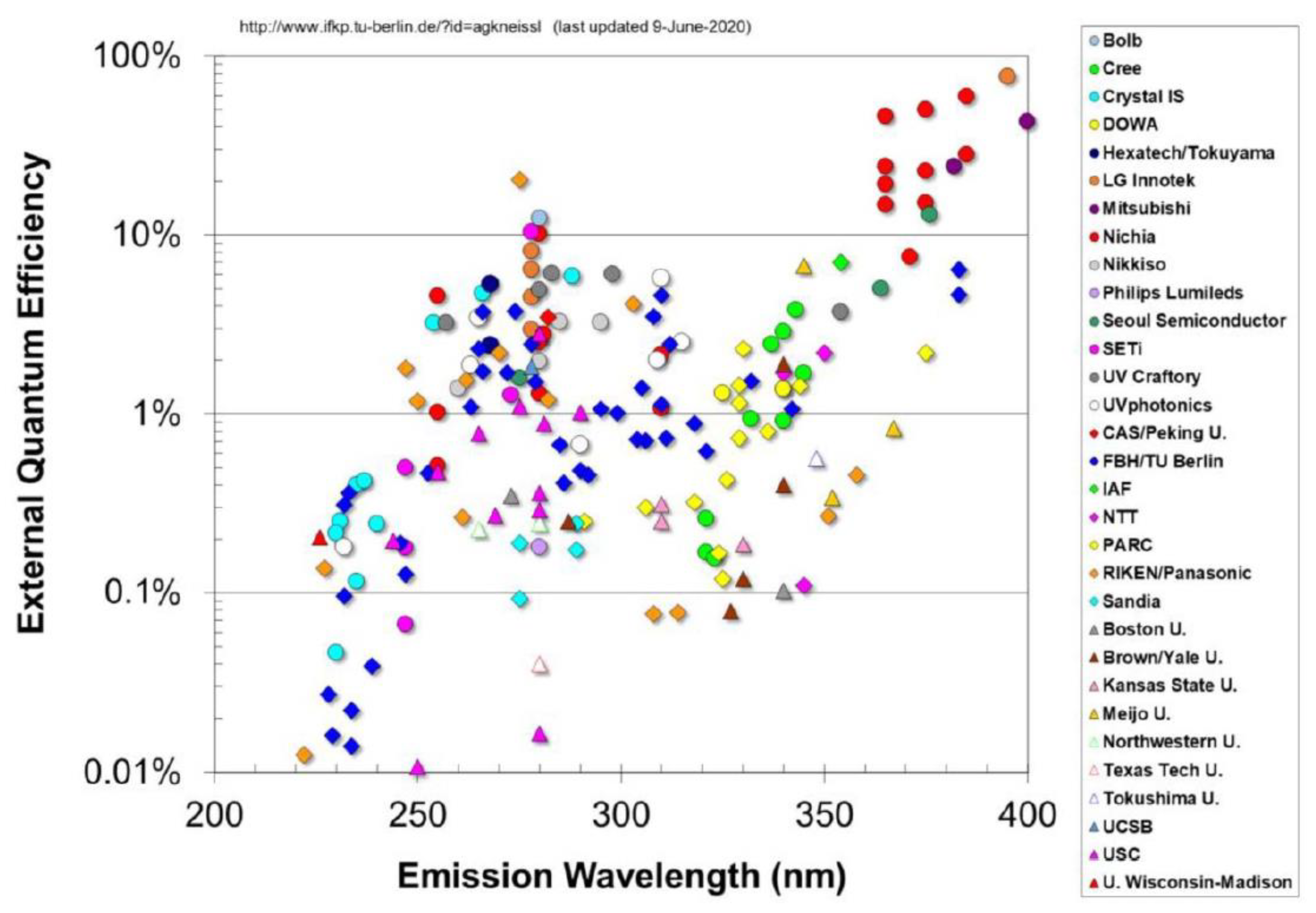
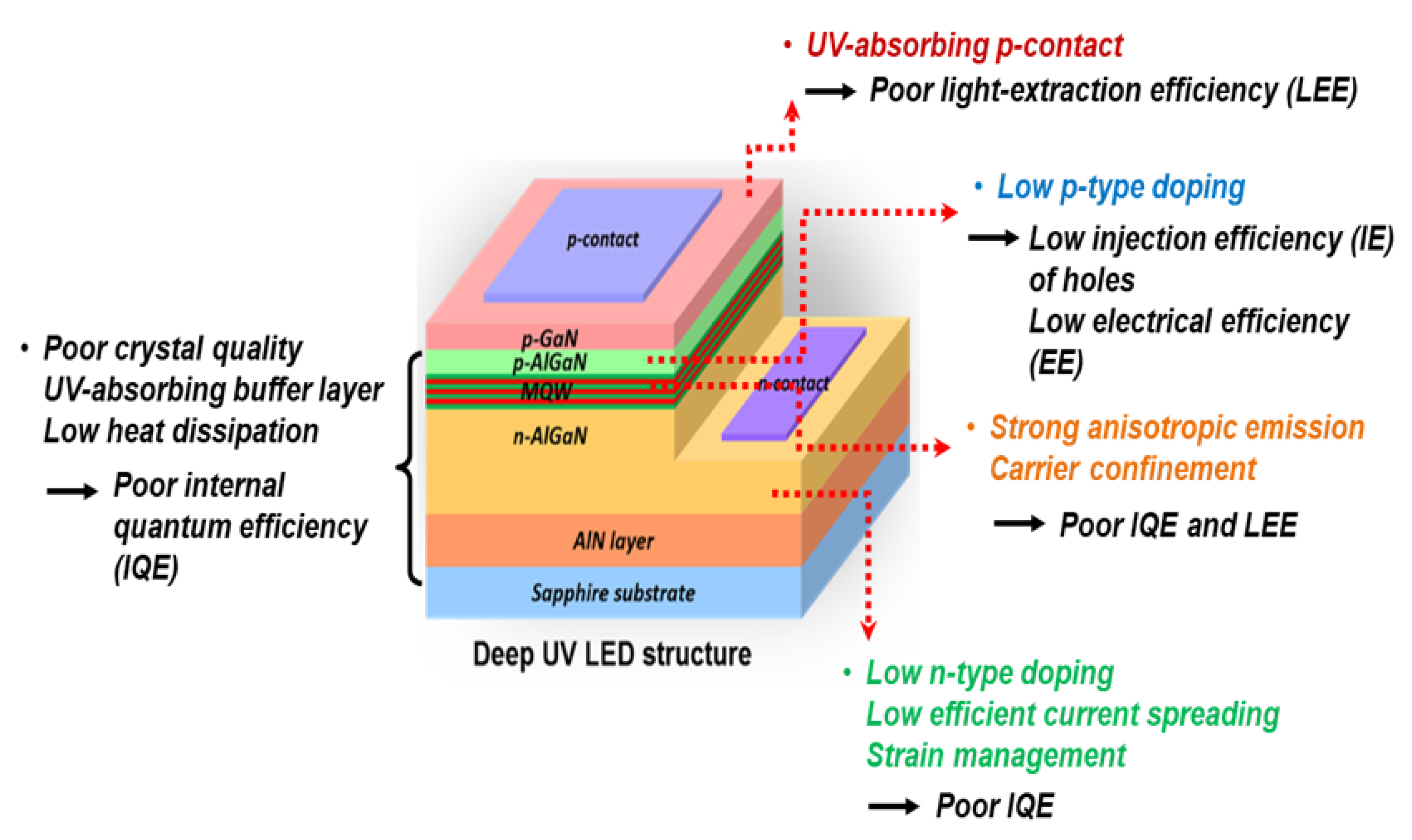
2.2. EQE of the Chip

Whereas InGaN-based active regions are used in LEDs that function via visible and near-UV radiation emission (400–465 nm), AlGaN-based LEDs enable light emission in the range between 265 and 365 nm, which are caused mainly by band-to-band transition and are much more sensitive to junction temperatures because of smaller carrier-confining and localization potentials. Therefore, it is a challenge to improve IQE in high-Al-content AlGaN-based LEDs.
The EQE (ηe) is used to measure the luminous efficiency of LED chips. Its computation is shown in Equation (1):
η e = ξ e x η i = ξ e x n p h n e .
In this equation, ηi (IQE) is the ratio of the number of photons generated in the active zone (nph) and the number of injected electrons (ne) with unit time, and ξ ex (LEE) is the ratio of the number of photons entering the outer space and the total number of generated photons. Therefore, the EQE of LED chips is closely related to the chip quality and LEE. However, as the emission wavelength changes from blue to UV, the ηi of the group nitride LED chip usually gradually decreases [15]. In UVC LED sterilization and disinfection equipment, the radiation illuminance of a single UV LED often does not fulfill the inactivation dose requirement, which must be compensated by multiple integrated packages. Although the UVC LED chip has a device structure similar to that of the blue LED, the higher Al composition of the former significantly differentiates its chip quality from that of the latter, such as the lower LEE, which comes from the larger mismatch in the MQWs. At present, EQE improvement of UVC chips remains subject to the following bottlenecks, as shown in Figure 3.

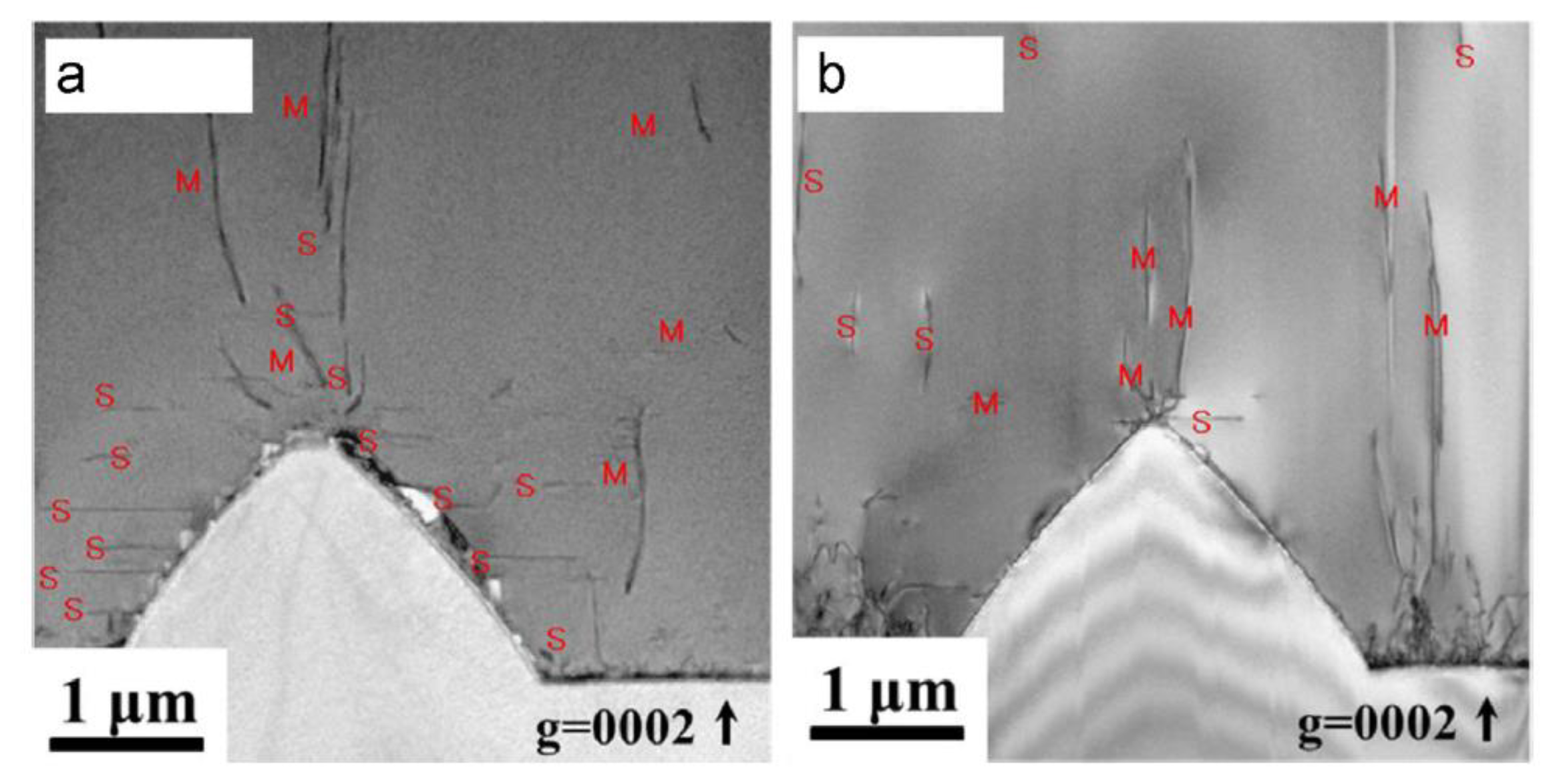
2.2.1. Immature Epitaxial Technology of High-Al-Content Nitride Semiconductor

(A) The substrate is the basis of the epitaxial growth of a chip; therefore, the selection of its material has a vital role in the quality of the chip. The selection of substrate material and its application should follow the three principles: matching lattice constant and thermal expansion coefficient, high thermal conductivity, and low light absorption. Among blue chips, sapphire (Al2O3) is widely used as the substrate. Similarly, based on extensive studies on epitaxial technology, sapphire substrates have become widely used in the production of UVC chips. Meanwhile, the material in the active region of a typical 275 nm UVC LED used for sterilization is Al0.4Ga0.6N/Al0.47Ga0.53N MQWs [17]. Additionally, to solve the problem of lattice mismatch between sapphire and AlGaN, AlN is usually first grown as a buffer layer on a sapphire substrate, which is followed by growth of the AlGaN epitaxial structure. Since the band gap of AlN is higher than the energy of UVC photons, there is no light absorption problem. However, the lattice mismatch and thermal mismatch between sapphire and AlN materials are both large [18,19]; therefore, when AlN is grown on the surface of sapphire, abnormal growth often occurs at the interface of crystal grains [20]. Under normal circumstances, the direction of epitaxial growth should be along the (0001) crystal orientation of the sapphire substrate. However, because of the high degree of lattice mismatch during the initial period of growth, the direction of AlN growth is relatively random, forming a variety of “anomalous islands”. Only when the growth thickness is large enough will these “anomalous islands” be covered by the normally grown lattice, but the dislocations they had caused will extend to the upper layer and affect the quality of the epitaxial layer. Therefore, reducing the dislocation density of the interface between the sapphire substrate and AlN is particularly critical. The use of high-temperature epitaxy or annealing can reduce the dislocation of the buffer layer interface to a certain extent [21]. Miyake et al. suggested the use of sputtered and annealed AlN as a template for growing LED structures. They studied the effects of annealing an AlN buffer layer in a carbon-saturated N2–CO mixture on the growth of high-quality AlN on a sapphire substrate. The effects of annealing were investigated as a function of the AlN buffer layer thickness and annealing temperature [22,23]. The Chen Changqing team of Huazhong University of Science and Technology experimented with adjusting the epitaxial growth temperature. After the growth of an AlN epitaxial layer at 750 °C, the temperature was increased to 1250 °C to grow another layer of AlN, after which normal epitaxial growth proceeded. Among these layers, the AlN layer grown at high temperature can act as a dislocation shield [24]. Kneissl et al. at the Technical University of Berlin, Germany used a patterned sapphire substrate (PSS) to grow an AlN buffer layer and performed high-temperature annealing at 1700 °C, which increased the LEE by nearly 15%, from 3.4% to 3.9% [25]. Chiu et al. of Hsinchu Chiao Tung University utilized a sputtered AlN nucleation layer grown on a PSS to enhance the quality of their epitaxial layer. The threading dislocation densities (TDDs) were reduced from 6 × 107 cm−2 to 2.5 × 107 cm−2 at the interface between the u-GaN layers in conventional and AlN PSS devices, respectively [26]. The results are shown in Figure 4. In a later study, this group also proposed the preparation of an AlN template via re-growth on a sputter-deposited AlN buffer layer. Before growth, the buffer layer was thermally annealed and then underwent AlN regrowth during metal–organic chemical vapor deposition (MOCVD) at a threading dislocation density of less than 5.0 × 108 cm−2. At the same time, the absorption rate of the light with the 280 nm wavelength that propagated through the template was less than 6% [27].
The crystal orientation of sapphire is also one of the factors affecting the quality of epitaxy. In particular, changing the chamfer angle of the sapphire substrate can modify the IQE of the chip [28]. For example, Sun et al. from the University of Science and Technology of China epitaxially grew AlN on a beveled sapphire substrate and determined that when the growth angle differs from the (0001) crystal plane angle by 4°, small dots will cause the localization of carriers and increase luminous efficiency [29]. A chamfer angle of 4° has also been reported to inhibit the growth of irregular grains at the interface [30]. When the substrate is arranged into a periodic concave–convex pattern, it can effectively inhibit the development of dislocations during the epitaxial growth process and annihilate them in the early stage of formation [31,32,33]. For instance, the group of Wang Junxi of the Institute of Semiconductors of the Chinese Academy of Sciences grew an AlN buffer layer on a patterned sapphire substrate, which enabled reducing the thickness of the buffer layer and improved the IQE of the UVC LED [34]. Zhou et al. developed a patterned sapphire substrate with periodic inlays of SiO2, which effectively reduced interface dislocations and increased the EQE of their UVA LED by 26.1% compared with that of the traditionally patterned substrates [35]. In addition to optimizing the sapphire substrate and epitaxial technology, the selection of other new substrate materials, such as AlN self-supporting substrates, semi-polar surface substrates, is another potential route to the improvement of UV LED technology [36,37,38].
(B) The growth of AlGaN with high Al content in the AlxGa1−xN ternary mixed crystal is also one of the obstacles to high-quality epitaxy. The surface viscosity coefficient of Al atoms is higher than that of GaN, which lowers the mobility during epitaxial growth. The newly grown Al cannot choose the lowest energy nucleation site to which to attach, and thus even with a buffer layer, many point defects and dislocations develop in the active region. These different types of defects act as non-radiative recombination centers, consuming carriers that should participate in band-edge radiative luminescence. To counteract these problems, the research team of Zhang Rong of Xiamen University and Liu Bin of Nanjing University adopted a flow-modulated epitaxy technology using an ammonia atmosphere, which enhanced the mobility of Al atoms and greatly improved the epitaxial quality of the AlGaN/AlN interface [39].
(C) In addition to optimizing the substrate and AlxGa1-xN ternary mixed crystal, it is also necessary to improve the epitaxial structure of the quantum well in the active region, so that the holes and electrons in the active region are effectively constrained, and the overlap of the hole–electron wave function is improved. The use of stepped Al component barrier regions in quantum wells can effectively improve the recombination efficiency of holes and electrons [40,41]. Studies have shown that the use of GaN/AlN structures in quantum wells can significantly improve the quantum efficiency [42]. However, because the band gap of GaN is quite low, it is necessary for the well layer to be very thin, such that the quantum confinement effect can be used to raise the band-edge energy level. Kobayashi et al. of Kyoto University, Japan, recently successfully developed a GaN quantum well with a single atomic layer, with a peak emission wavelength near 225 nm, and increased its EQE to 5% [43]. Similarly, the team of Li Xiaohang of King Abdullah University of Science and Technology in Saudi Arabia achieved a 249 nm UVC laser output by growing a four-atomic layer GaN well region and a six-atomic layer AlN barrier region [44].
(D) Control of the growth of AlN and its interface with the sapphire substrate is one of the key issues in developing high-efficiency UV optoelectronic devices. The low LEE arises from large amounts of transverse magnetic (TM)-polarized light [45], the highly absorptive p-GaN ohmic contact layer [46], the total internal reflection (TIR), and Fresnel loss caused by the large refractive index contrast between AlGaN and air [47]. Migration-enhanced metal–organic chemical vapor deposition (ME-MOCVD) [48,49,50] and the pulsed-flow multilayer AlN buffer growth technique [51] are proposed to improve the quality of Al-rich AlGaN layers. When the LEE was thus improved, the EQE for DUV LEDs grown on nano-patterned sapphire substrate (NPSS) reportedly reached 20% [9,52]. Moreover, the IQE is also an important factor that influences the EQE of UV optoelectronic devices. Wuu et al. from National Chung Hsing University of Taiwan successfully demonstrated the growth of high-IQE AlGaN MQWs on low-defect-density AlN templates using NPSS. These templates consisted of AlN structures with 0–30-period superlattices (SLs) that alternated high (100) and low (25) V/III ratios under a low growth temperature (1130 °C). Through optimization of the SL period, the AlN crystallinity was systematically improved, and an ultra-low etch pit density was achieved. The relative IQE of 280-nm AlGaN MQWs dramatically increased from 22.8% to 85% when the inserted SL was increased from 0 to 20 periods [53]. On the other hand, p-type conductivity for high-Al-content AlGaN has recently been achieved using distributed-polarization-induced 3D hole gas [53,54]. The numerous approaches on the improvement of UV LED efficiencies such as the modified quantum barriers were deeply investigated [55,56]. These designs will be helpful for suppressing the efficiency droop in AlGaN-based UVC LEDs.

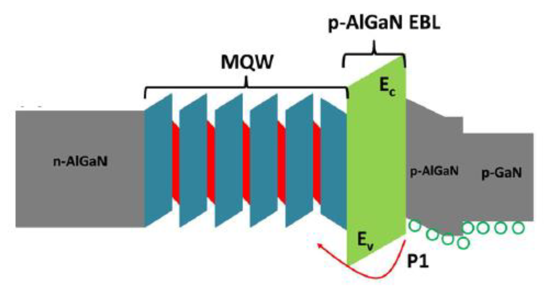
2.2.2. Carrier Transport and Internal Quantum Efficiency

DUV LEDs require effective control of n-type conductivity in n-AlGaN layers and good control of p-type conductivity in Al-rich p-EBL, p-AlGaN layers, and p-GaN layers. However, as the Al content in AlGaN is increased, the cohesive energy and bond strength increase rapidly, and control of the electronic properties through doping becomes non-trivial. Therefore, a number of strategies have been devised to push the limits of the n and p-type doping of AlGaN materials for efficient carrier injection into the active regions of UV LEDs. Early theoretical research predicted that Si substitutionally incorporated on column IIIA cation sites should remain a stable hydrogen-like donor over the entire AlGaN alloy composition [57,58]. At present, resistivities of or below 10−2 Ω cm can be achieved for n-AlGaN layers with an Al composition of up to 80% [59]. However, the high ionization energy of p-type Mg doping in a hole injection layer leads to insufficient effective hole density. Currently, the main doping method for a p-type layer is to dope Mg in AlGaN. The activation energy of Mg in AlGaN ranges from 0.17 eV (GaN) to 0.52 eV (AlN) [60]. Such a high activation energy makes it difficult for the Mg acceptor to generate effective holes, and thus, the number of holes generated after the device is switched on is much smaller than the number of electrons generated in the n-type layer, resulting in insufficient holes for generating electron–hole pairs in the active region. In addition, under high excitation densities, some electrons cross the active region and enter the p-type layer, forming parasitic radiation from the p-type layer [20,61]. In the case of AlGaN, a rising Al mole fraction raises the electron band gap energy. Therefore, to enhance hole injection through a graded AlGaN layer into the active region, the Al mole fraction should be at its lowest near the active region. However, the typical Ga-face growth process of nitride structures generates a positive polarization charge within such a graded AlGaN layer, which does not attract free holes. Thus, N-face growth must be utilized to generate negative bulk charges in the graded AlGaN layer. Afterward, the internal quantum efficiency can be strongly increased and the efficiency droop eliminated using such a graded AlGaN layer instead of a traditional AlGaN electron-blocking layer (EBL) [62]. Numerous designs, including AlGaN superlattices and graded layers [53,63,64,65], have been demonstrated to allow the polarization fields to assist the ionization of Mg acceptors. To overcome the problem of solubility [66] and tendency of self-compensation, delta-doping, or modulation-doping techniques have been investigated for p-AlGaN.
Another way of improving IQE is through setting up an EBL with a high electron barrier between the active region and the p-type layer, which can alleviate electron overflow to a certain extent [67]. However, the electron blocking layer will also reduce the emissivity of holes. Figure 5 shows a typical DUV device energy-band structure with a p-AlGaN blocking layer [68]. A similar structure was designed by the team of Ge Weikun of Beijing University as a multilayer electron barrier layer with gradual changes in thickness and Al composition. While suppressing the overflow of electrons, it also increased the emissivity of holes and greatly improved quantum efficiency [69]. Meanwhile, Hu et al. reported that an electron deceleration layer with a superlattice structure can be added between the n-type layer and the active region to alleviate the electron overflow effect [70]. Other innovative methods that have achieved good results include that developed by the team of Dai Jiangnan of Huazhong University of Science and Technology, who replaced the p-type layer monolithic integration technology with a multiplicative photoelectric converter (MPC), which can absorb part of the active area emission [71].
The aforementioned two problems not only lead to decreases in the quantum efficiency of the chip but also cause parasitic peaks in the light band of its electro-luminescence spectrum [72]. Although parasitic peaks are usually considered to be due to the impurity radiation level, the epitaxial layer where the impurity is located has not been explored in this context. Lin Yue et al. conducted in-depth research on UV LEDs of multiple wavelengths and proposed new ideas on the source of parasitic peaks. The study determined that in the luminescence spectrum of UVC LEDs with a wavelength of 275 nm, the parasitic peaks at approximately 400 nm are more obvious at ultra-low and high excitation density, but they are difficult to observe at medium excitation density. These parasitic peaks are believed to originate from two regions as radiation recombination defects: one located in the quantum well, and the other in the p-type layer. They emit light at low and high excitation densities, respectively, and thus, parasitic peaks that appear in the same wavelength region can originate from different regions and different types of crystal lattice defects [73]. The study of these parasitic peaks can determine the quality of the epitaxial layer of a device from one side and elucidate the mechanism of carrier transport, which provides a reference for the improvement of device epitaxy in the future. In addition, this group conducted research on the point-defect recombination in UV LED (i.e., Shockley–Read–Hall recombination, trap-assisted recombination), leakage current, Auger recombination, and other factors that affect the quantum efficiency [74]. On the other hand, Kneissl et al. inferred that efficiency droop in AlGaN quantum-well heterostructures are caused by an internal carrier loss process, analogous to what occurs in an InGaN system. This loss process may be due to Auger recombination, where C = 2.3 × 10⁻³⁰ cm6 s−1; a similar value is commonly observed in InGaN-based devices [75]. In both these devices, point-defect recombination is a process in which the carrier recombination center formed by an impurity energy level in the band gap absorbs carriers that should have participated in band-edge radiation recombination at a low excitation density, such that they can undergo non-radiative recombination and result in leakage current. Although many mechanisms have been identified, all of them involve carriers bypassing the active region through a number of dislocation paths; therefore, these carriers do not participate in the process of band-edge radiation recombination. For example, the aforementioned electrons cross the active region and enter the p-type layer. Meanwhile, as a type of leakage current, Auger recombination is the process of transferring energy radiated by a pair of carriers that should radiate photons to excite a third carrier (hole or electron) into the band edge. These three mechanisms have been reported to reduce radiation recombination efficiency. Moreover, these three non-radiative recombination mechanisms change with temperature and excitation density, not only in terms of intensity, but also in terms of certain constraints between each other [74]. These methods can provide a reference for the effective operating current of a given device.

2.2.3. Problem of Light Extraction Efficiency

When ultraviolet photons are generated in a chip, they need to be radiated to the outside space through the chip–air interface. Compared with air, the chip is an optically dense medium. At the interface, some photons are reflected back into the chip because of the total reflection effect. The main measures to improve the efficiency of light extraction are surface roughening [76], the use of a micro-lens [77], and the use of photonic crystals [78,79], among other methods. Wang Junxi’s team of the Institute of Semiconductors of the Chinese Academy of Sciences used photolithography to fabricate a 274 nm UVC LED with a nanopillar structure, which also improved IQE and LEE [80]. The former improvement was due to the sidewalls of the nanopillars facilitating dissociation of excitons into free electron–hole pairs, which improved recombination efficiency, whereas the latter was due to the nanopillars producing an optical waveguide effect, which was beneficial to the export of photons. As a result, the total output optical power was increased 2.5-fold [80]. At the same time, the optical performance of the electrode must be optimized. If the electrode is in the light-emitting channel, the electrode must be transparent. On the other hand, if the electrode is at the bottom, it is necessary to increase its reflectivity in the UVC band to reflect the photons directed toward the substrate direction and facilitate extraction. Optimizing electrode design has been reported to improve LEE to a certain extent [81]. Another perspective for improving LEE is through the use of suitable packaging materials. For example, Prof. Hao-Chung Kuo’s group of National Chiao Tung University studied the LEE of new packaging materials. Through the addition of silicone oil, which had a refractive index of 1.487, to adjust the refractive index changes inside and outside the UV chip, and rational selection of the material of the reflector, to adjust reflectivity, the light output power of the UV LED was increased by 70.7% compared with that of a traditional package, whereas the thermal resistance was reduced by 30.3% [82]. Meanwhile, Wang et al. proposed a new encapsulation structure for aluminum nitride-based DUV-LEDs and eutectic flip chips containing polydimethylsiloxane (PDMS) fluid doped with SiO2 nanoparticles (NPs) with a UV-transparent quartz hemispherical glass cover. The optical output power of the proposed encapsulation structure was 81% higher than that of a traditional encapsulation structure [83]. In the aforementioned two cases, liquid materials with medium refractive index were utilized to enhance the radiated cone angle of light output from the chip, apply total internal reflection and Fresnel scattering to scatter light into the escape cone, and finally focus the light through the integration of a lens.

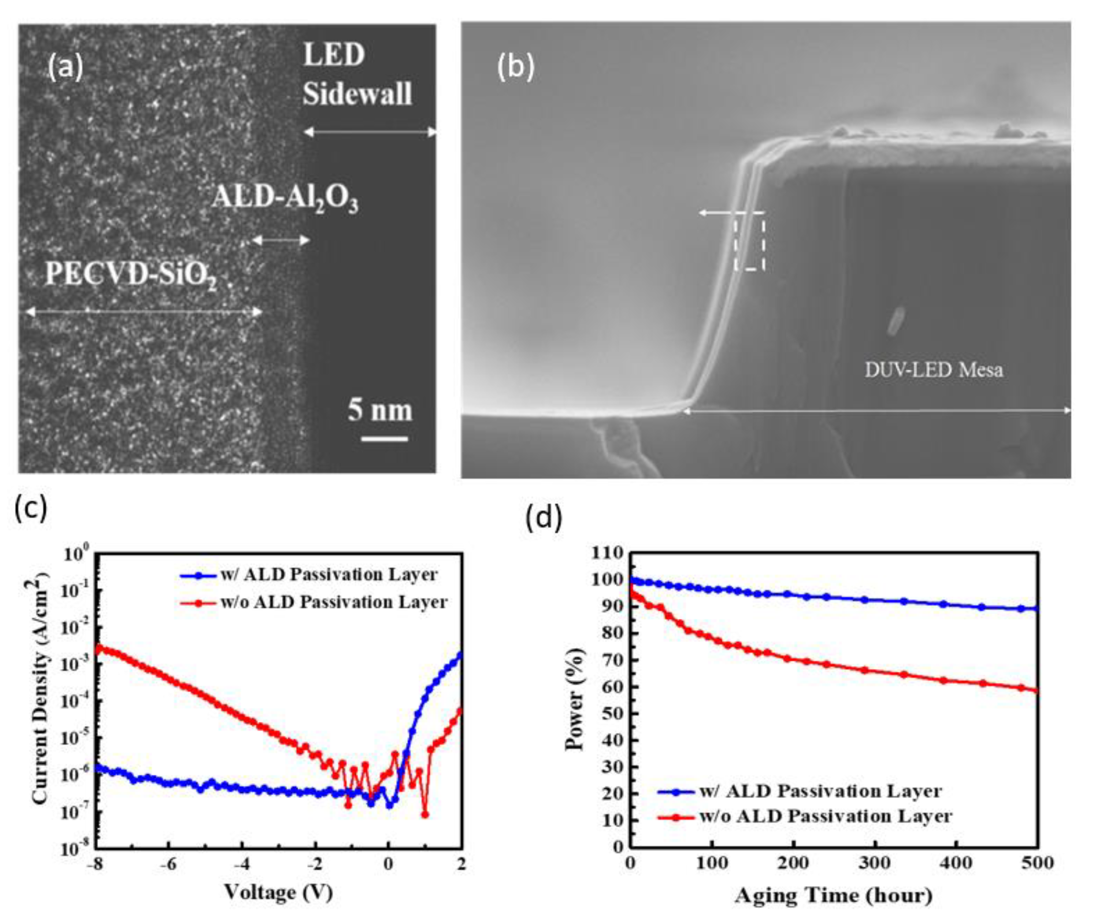
2.2.4. Improvement of Reliability through ALD Film Passivation

GaN-based blue LEDs have a long life with the Mean Time Between Failure (MTBF) up to 50,000 h [84]. However, UVC LEDs have larger lattice mismatch between AlGaN layers; therefore, its reliability is much shorter than GaN-based blue LEDs [84]. To attain maximum light output and long operating lifetime, LED chips require surface passivation to eliminate parasitic currents caused by traps and defects. In addition, a barrier coating is typically necessary because LED materials are sensitive to moisture. Atomic layer deposition (ALD) is an ideal technique to manufacture both the passivation and barrier films. In particular, when the LED sizes diminish to micrometer dimensions, it is the only coating method that is capable of producing high-quality films on the required minuscule scale. Ultra-thin, pinhole-free ALD films do not suppress the LED light intensity and provide reliable protection against ambient conditions, whereas their superior conformality ensures no thickness variations between the facets of the LED chip. Thickness variations, which are typical side effects of other coating methods, can potentially lead to uneven distribution of film stress or thermal expansion behavior and physical damage to the chip. In one study, deep UV LED chips were covered via SiO2/Al2O3 passivation, SiO2 deposited via PECVD, and Al2O3 deposited via ALD. Good step coverage was observed in the mesa surface of the DUV chip, of which the SEM microscope images are shown in Figure 6a,b. Meanwhile, leakage current under reverse bias was found in the chip subjected to ALD passivation, and the current density was measured to be approximately 10−6 A/cm2, as shown in Figure 6c. The chips shown in Figure 6c were subjected to an aging test after stressing at 25 °C, 50 mA, and 60% humidity. The chips with ALD coating exhibited less than 10% power drop; whereas the control chips without ALD film exhibited approximately 40% power drop by the 500 h of stressing, as shown in Figure 6d.

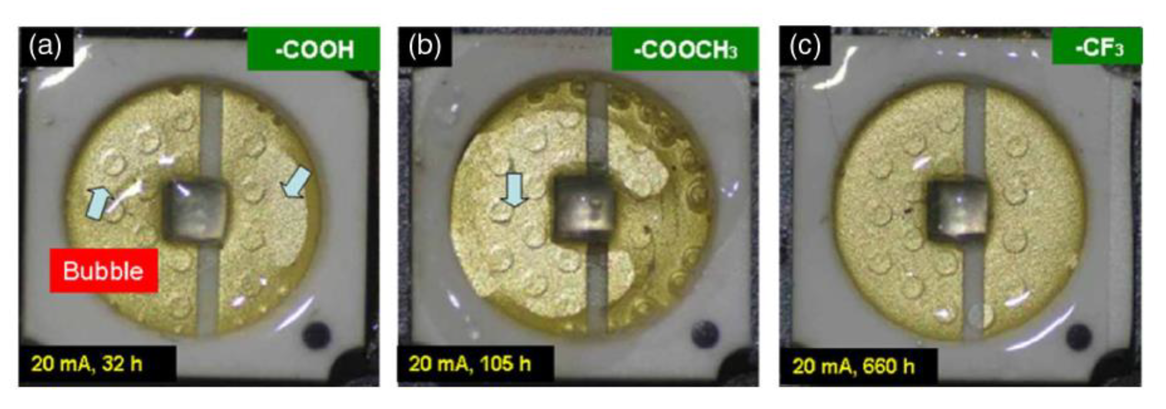
2.3. Packaging Material Aging Problem

For an LED light source, the package not only mechanically protects the light-emitting chip and circuit but also optimizes the LEE, effectively conducts chip heat, and reduces junction temperature [85]. To reduce costs, LEDs for general lighting use inexpensive and easy-to-process organic resin encapsulation; however, the most prominent problem with using UVC LED encapsulation materials is that organic materials are prone to aging and yellowing under long-term UVC band photon irradiation. For this reason, UVC LED packaging materials must account for three aspects: robustness, resistance to UV radiation, and effective light and heat conduction. In addition to using quartz glass as the lens, the combination of the lens and chip also requires the use of UV-resistant materials. Japan’s UV Craftory company uses fluorine-containing resin to replace traditional silica gel, which increases the working life of the packaging material from less than 1000 h to more than 6000 h [86]. However, the drawback of using fluorine-containing resin is that its refractive index is lower than that of silica gel, which is not conducive to forming a progressive layer of refractive indices that is beneficial to light extraction. According to comparisons of various fluororesins, silicone resin, and nonorgano materials, the only inorganomaterial known thus far for encapsulating DUV-LEDs is the polymerized perfluoro (4-vinyloxy-1-butene) (p-BVE) terminated with an –CF3 end group. In one study, through the formation of hemispherical lenses on DUV-LED dies using p-BVE with a –CF3 end group and a refractive index of approximately 1.35, the LEE was improved 1.5 times, demonstrating a cost-feasible packaging technique. Figure 7a–c show the aging results for p-BVE with –COOH, –COOCH3, and –CF3 end groups, respectively [86].

2.4. Thermal Management Issues

A high energy band gap and low conductivity can result in poor forward voltage characteristics when a UV LED is operated and therefore lead to higher power consumption. Part of the input electrical power contributes to the creation of light radiation; however, the remaining input electrical power is not used for radiation and is converted into heat, thus increasing the junction temperature. In turn, this accelerates the aging of devices and packaging materials. To solve the heating problem, in addition to the fundamental methods of enhancing the EQE, the heat dissipation efficiency must also be improved. Since the thermal conductivity of a sapphire substrate is 23.1 W/mK when parallel to the optical axis and 25.2 W/mK when perpendicular to the optical axis, both of which are relatively low values, inverting the chip is more conducive to heat dissipation from the direction of the substrate through the metal electrode [87]. Welding materials with high thermal conductivities, such as gold–tin eutectic solder or tin–silver–copper alloy solder, should also be used. Another possible welding material is gold–gold solder, which has been proven to have a similar effect to that of gold–tin eutectic soldering [88]. Furthermore, the substrate must be equipped with resistance to photo-degradation and good thermal conductivity. The blue LED sometimes requires a metal-based printed circuit board (MBPCB) that has both electrical connection and heat conduction functions as the substrate. However, the epoxy resin layer of an MBPCB is easily degraded by UVC radiation; thus, it is not suitable for use as a substrate for UVC LEDs. Meanwhile, for the submount, electronic ceramic materials such as AlN or Al2O3 may be used. However, these two materials are relatively brittle and easy to break. Therefore, to include both the flexibility of metal and insulation of ceramics into one material, the British Cambridge Nanotherm Company coated a very thin Al2O3 film onto the surface of an aluminum material, thus maintaining its overall flexibility. The thermal conductivity of an Al submount coated with thin Al2O3 can reach 152 W/mK, which is only slightly lower than that of AlN [89].

3. Deep Ultraviolet LED Sterilization Mechanism and Application

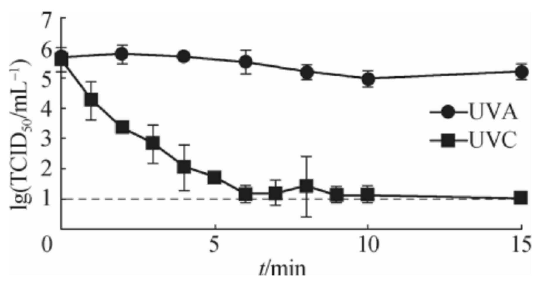
3.1. Killing Mechanism of Deep Ultraviolet LED on Viruses and Bacteria

Effective sterilization and disinfection materials need to be broad in scope, rapidly acting, and harmless to the environment. This research topic is especially relevant to the severe and ongoing pandemic of coronavirus disease 2019 (COVID-19). Research studies from Tel Aviv University (TAU) have proven UV LED disinfection of coronavirus [90]. In particular, UVC is capable of effectively killing the virus that causes COVID-19 [91]. Thus, research on UV LEDs in the field of sterilization focuses on the following requirements. DNA and RNA are the genetic materials of all organisms, and bacteria and viruses can be effectively killed or inactivated through the destruction of their DNA or RNA molecules. Bases are the fundamental elements of DNA and RNA long chains. The bases in DNA are adenine, guanine, thymine, and cytosine, whereas the bases in RNA are adenine, guanine, cytosine, and uracil. Studies have shown that both purines and pyrimidines (components of DNA and RNA) absorb UVC and UVB light, and that the absorption rate by pyrimidine is higher; thus, the main photochemical product is from the reaction of pyrimidine [92,93]. UV irradiation generates cyclobutene pyrimidine dimers and the pyrimidine–pyrimidinone photoproduct, which damage the structure of DNA and RNA molecules, affecting DNA replication and RNA transcription and translation as well as ultimately leading to cell apoptosis or virus inactivation. Since DNA and RNA are widely present in organisms, UV radiation is not aimed at specific microorganisms and is a broad-spectrum antibacterial tool.
After the Severe Acute Respiratory Syndrome (SARS) epidemic in 2003, research on the ability of UV to inactivate coronavirus has gained popularity. In 2004, the US Food and Drug Administration conducted a comparative study on mainstream virus inactivation methods [91]. In this study, a 254-nm UVC radiation source and 365-nm UVA light source irradiated two groups of samples from a distance of 3 cm. Each group of samples contained 24 virus culture dishes placed on ice. The experimental results are shown in Figure 8. In the control group irradiated with UVC, half of the tissue culture infectious dose (TCID50) decreased after 1 min, dropped to less than 0.01% of the initial value at 6 min, and remained at this level for 15 min after continued irradiation. The virus was completely inactivated at this stage. However, no significant decrease in TCID50 levels was observed in the UVA-irradiated control group. This indicates that the UVC band in ultraviolet light has a significant inactivation effect on the coronavirus. In addition, for comparison, high-temperature inactivation at 56 °C was demonstrated to require 20 min to achieve the effect of UVC irradiation for 6 min. The aforementioned results show that UVC disinfection is more efficient than high-temperature disinfection. However, more detailed irradiance comparisons and comparative studies on the inactivation effects of different UVC wavelengths have not been reported.

3.2. Deep Ultraviolet LED Disinfection Application

Although existing UVC LED disinfection products are often designed with reference to traditional mercury light source disinfection products, the spectral wavelengths of UVC LED (wavelength 260–280 nm) and mercury light source (wavelength 253.7 nm) are different. For Bacillus trophaeus spores, UV LEDs at 260 nm are at least as effective for inactivation microbes in water as conventional mercury light source [95]. Current research on the application of UV sterilization focuses mainly on the two directions of water sterilization and air sterilization.
The team of Zhang Baoping of Xiamen University conducted a more systematic study on the disinfection of water by deep ultraviolet LEDs. In the comparison of the detoxification effect of deep ultraviolet LEDs of different wavelengths and different intensities on water bodies, a wavelength of 275 nm was determined to have the most significant killing effect on Escherichia coli and effectively inhibited the regeneration of bacterial colonies [96]. In a comparative study of UV LEDs with different driving conditions on water disinfection, pulse-driven deep ultraviolet LEDs were recommended for disinfection under long-term working conditions [91]. In another study, the addition of TiO2 photocatalyst to water resulted in the generation of active oxygen ions by the photolysis of water under UVC irradiation, which increased the disinfection effect, and a 275 nm UV LED combined with TiO2 photocatalyst was recommended to be the best solution for killing E. coli [97]. These results also have been verified by similar research in the industry [98]. With regard to the application of UVC LED to drinking water sterilization and disinfection, Matsumoto et al. of Nagoya City University in Japan designed a device that uses water waveguide technology to improve the utilization efficiency of UVC radiation sources. As shown in Figure 9, UVC passes through the water waveguide; then, the water flow in the water pipe can be irradiated for a long time, which effectively improves sterilization efficiency [99].
In a research study on air sterilization using UV radiation, Rudnick et al. from Harvard University in the United States determined that a UV sterilization device in a heating, ventilation, and air conditioning (HVAC) appliance is more efficient than a portable one [100]. Similarly, Yang et al. of the City University of Hong Kong, in collaboration with other teams, performed research on air sterilization. An environmental room was equipped with an upper-room ultraviolet germicidal irradiation (UR-UVGI) device (upper-level UV sterilization technology; the UVGI is installed in the upper part of the room only to irradiate the upper air) against Serratia marcescens, Staphylococcus epidermidis, Staphylococcus epidermidis, alkali-producing Pseudomonas (Pseudomonas alcaligenes), and Micrococcus luteum (Micrococcus luteus), and other common bacteria, etc. After a series of sterilization experiments, it was concluded that the use of UR-UVGI can reduce bacterial concentration in the respiratory area under low-pass rates, and the bacterial-inactivation effect of UR-UVGI is reduced as the ventilation rate is increased. Therefore, UR-UVGI can generally be used in poorly ventilated rooms to prevent the inflow of airborne pathogens [101]. In a study of the relationship between UVC dosage and air sterilization effect, a ventilation-duct UVGI system was designed to test its capabilities against five airborne pathogens (Serratia marcescens, Pseudomonas alcaligenes, E. coli, Salmonella enteritidis, and Staphylococcus epidermidis) [102]. The experimental results showed that the UVGI device installed in the HVAC piping system may provide a supplementary solution for improving indoor the air quality in a mechanical ventilated or air-conditioned environment; however, it should produce the exact amount of UV radiation received by bacteria in air. Regarding the flow rate, environmental factors such as temperature, humidity, and pipe reflectivity have an impact on the UVC lamp with sensor. Performance impact studies have also shown that with an increase in air velocity and relative humidity, the bactericidal effect decreases to a certain extent [103]. Comparison of UVC to performance ratio at low (15–16 °C) and higher temperatures (25–26 °C) reveal that UVC has a maximum sterilization effect at a temperature of 20–21 °C.

4. Conclusions and Outlook

AlGaN-based UVC-LEDs have low EL output due to their low EQE. This limitation is due to the insufficient crystallinity of AlN templates on sapphire substrates. Before growth, the buffer layer was thermally annealed, and then, it underwent AlN regrowth during metal–organic chemical vapor deposition (MOCVD), and a threading dislocation density of less than 5.0 × 108 cm−2. The poor crystal quality is partly due to the large lattice and thermal mismatch between Al-rich AlGaN layer and sapphire substrate. The low LEE arises from a large amount of transverse magnetic (TM)-polarized light, the highly absorptive p-GaN ohmic contact layer, and total internal reflection (TIR) and Fresnel loss caused by the large refractive index contrast between AlGaN and air. Numerous approaches on the improvement of UV LED efficiencies include the replacement of the conventional AlGaN electron blocking layers with modified EBLs. The internal quantum efficiency can be also strongly increased and the efficiency droop eliminated using polarization-doped graded AlGaN layers. For UVC LEDs, which are dominated by TE-polarized emission, improving the contact layer transparency is more essential for power enhancement.
Specifically, UVC LEDs with ALD Al2O3 passivation and normal LED packaging (no hermetic seal) maintained 90% of its original efficiency even after 500 h environmental test at 60% humidity and 25 °C. However, UVC LED packaging materials must account for three aspects: robustness, resistance to UV radiation, and effective light and heat conduction. One promising material is fluorine-containing resin, which increases the working life of the packaging material from less than 1000 h to more than 6000 h. Finally, we discussed the mechanism of UVC sterilization and hope that UVC LEDs will have broader applications in killing viruses such as the COVID-19 virus.

Author Contributions

Data curation, K.-H.C., K.-K.Y., P.-T.L. and Y.L.; project administration, Z.C. and H.-C.K.; writing—original draft, T.-C.H., Y.-T.T. and Y.-W.Y.; writing—review and editing, T.W., X.F. and S.-H.L. All authors have read and agreed to the published version of the manuscript.

Funding

Ministry of Science and Technology, Taiwan (107-2221-E-009-113-MY3, 108-2221-E-009-113-MY3); Hsinchu Science Park Bureau, Ministry of Science and Technology, Taiwan (108A08B); National Natural Science Foundation of China (11904302); Fundamental Research Funds for the Central Universities (0621ZK1022).

Acknowledgments

The authors would like to thank APT Corp, Junyong Kang of Xiamen University, Chia-Yen Huang of National Yang Ming Chiao Tung University, Hideto Miyake of Mie University and Ricky Lee of Hong Kong University of Science and Technology for their helpful support.

Conflicts of Interest

The authors declare no conflict of interest.

References

  1. Pankove, J.; Duffy, M.; Miller, E.; Berkeyheiser, J. Luminescence of insulating Be-doped and Li-doped GaN. J. Lumin. 1973, 8, 89–93. [Google Scholar] [CrossRef]
  2. Han, J.; Crawford, M.; Shul, R.; Figiel, J.; Banas, M.; Zhang, L.; Song, Y.; Zhou, H.; Nurmikko, A. AlGaN/GaN quantum well ultraviolet light emitting diodes. Appl. Phys. Lett. 1998, 73, 1688–1690. [Google Scholar] [CrossRef]
  3. Lambert, J.; Shurvell, H.; Lightner, D.; Cooks, R. Organic Structural Spectroscopy; Prentice-Hall Inc.: Upper Saddle River, NJ, USA, 1998. [Google Scholar]
  4. Kneissl, M.; Rass, J. III-Nitride Ultraviolet Emitters; Springer: Berlin/Heidelberg, Germany, 2016. [Google Scholar]
  5. LEDinside. Deep UV LED Application Market- Sterilization, Purification, and Water Treatment Markets; LEDinside: Taipei, Taiwan, 2019. [Google Scholar]
  6. Hirayama, H. Growth of (In) AlGaN compound semiconductors and their application to 300-nm-band high-intensity UV-LEDs. Rev. Laser Eng. 2002, 30, 308–314. [Google Scholar] [CrossRef] [Green Version]
  7. Amano, H.; Collazo, R.; De Santi, C.; Einfeldt, S.; Funato, M.; Glaab, J.; Hagedorn, S.; Hirano, A.; Hirayama, H.; Ishii, R. The 2020 UV emitter roadmap. J. Phys. D Appl. Phys. 2020, 53, 503001. [Google Scholar] [CrossRef]
  8. Narukawa, Y.; Ichikawa, M.; Sanga, D.; Sano, M.; Mukai, T. White light emitting diodes with super-high luminous efficacy. J. Phys. D Appl. Phys. 2010, 43, 354002. [Google Scholar] [CrossRef]
  9. Takano, T.; Mino, T.; Sakai, J.; Noguchi, N.; Tsubaki, K.; Hirayama, H. Deep-ultraviolet light-emitting diodes with external quantum efficiency higher than 20% at 275 nm achieved by improving light-extraction efficiency. Appl. Phys. Express 2017, 10, 031002. [Google Scholar] [CrossRef]
  10. Endruweit, A.; Johnson, M.; Long, A. Curing of composite components by ultraviolet radiation: A review. Polym. Compos. 2006, 27, 119–128. [Google Scholar] [CrossRef]
  11. Decker, C. The use of UV irradiation in polymerization. Polym. Int. 1998, 45, 133–141. [Google Scholar] [CrossRef]
  12. Schreiner, M.; Martínez-Abaigar, J.; Glaab, J.; Jansen, M. UV-B induced secondary plant metabolites: Potential benefits for plant and human health. Optik Photonik 2014, 9, 34–37. [Google Scholar] [CrossRef]
  13. Hockberger, P.E. A History of Ultraviolet Photobiology for Humans, Animals and Microorganisms. Photochem. Photobiol. 2002, 76, 561–579. [Google Scholar] [CrossRef]
  14. Kneissl, M.; Seong, T.-Y.; Han, J.; Amano, H. The emergence and prospects of deep-ultraviolet light-emitting diode technologies. Nat. Photonics 2019, 13, 233–244. [Google Scholar] [CrossRef]
  15. Chu, C.; Tian, K.; Che, J.; Shao, H.; Kou, J.; Zhang, Y.; Li, Y.; Wang, M.; Zhu, Y.; Zhang, Z.-H. On the origin of enhanced hole injection for AlGaN-based deep ultraviolet light-emitting diodes with AlN insertion layer in p-electron blocking layer. Opt. Express 2019, 27, A620–A628. [Google Scholar] [CrossRef] [PubMed]
  16. Park, J.-S.; Kim, J.K.; Cho, J.; Seong, T.-Y. Group III-nitride-based ultraviolet light-emitting diodes: Ways of increasing external quantum efficiency. ECS J. Solid State Sci. Technol. 2017, 6, Q42. [Google Scholar] [CrossRef]
  17. Zhang, J.; Wu, S.; Rai, S.; Mandavilli, V.; Adivarahan, V.; Chitnis, A.; Shatalov, M.; Khan, M.A. AlGaN multiple-quantum-well-based, deep ultraviolet light-emitting diodes with significantly reduced long-wave emission. Appl. Phys. Lett. 2003, 83, 3456–3458. [Google Scholar] [CrossRef]
  18. Wang, J.; Yan, J.; Guo, Y.; Zhang, Y.; Tian, Y.; Zhu, S.; Chen, X.; Sun, L.; Li, J. Recent progress of research on III-nitride deep ultraviolet light-emitting diode. Sci. Sin. Phys. Mech. Astron. 2015, 45, 067303. [Google Scholar]
  19. Moustakas, T.D.; Paiella, R. Optoelectronic device physics and technology of nitride semiconductors from the UV to the terahertz. Rep. Prog. Phys. 2017, 80, 106501. [Google Scholar] [CrossRef]
  20. Heffelfinger, J.; Medlin, D.; McCarty, K. On the initial stages of AlN thin-film growth onto (0001) oriented Al2O3 substrates by molecular beam epitaxy. J. Appl. Phys. 1999, 85, 466–472. [Google Scholar] [CrossRef]
  21. Teramura, S.; Kawase, Y.; Sakuragi, Y.; Iwayama, S.; Iwaya, M.; Takeuchi, T.; Kamiyama, S.; Akasaki, I.; Miyake, H. High Crystallinity and Highly Relaxed Al0.60Ga0.40N Films Using Growth Mode Control Fabricated on a Sputtered AlN Template with High-Temperature Annealing. Phys. Status Solidi A 2020, 217, 1900868. [Google Scholar] [CrossRef]
  22. Miyake, H.; Lin, C.-H.; Tokoro, K.; Hiramatsu, K. Preparation of high-quality AlN on sapphire by high-temperature face-to-face annealing. J. Cryst. Growth 2016, 456, 155–159. [Google Scholar] [CrossRef] [Green Version]
  23. Miyake, H.; Nishio, G.; Suzuki, S.; Hiramatsu, K.; Fukuyama, H.; Kaur, J.; Kuwano, N. Annealing of an AlN buffer layer in N2–CO for growth of a high-quality AlN film on sapphire. Appl. Phys. Express 2016, 9, 025501. [Google Scholar] [CrossRef] [Green Version]
  24. Zhang, Y.; Long, H.; Zhang, J.; Tan, B.; Chen, Q.; Zhang, S.; Shan, M.; Zheng, Z.; Dai, J.; Chen, C. Fast growth of high quality AlN films on sapphire using a dislocation filtering layer for ultraviolet light-emitting diodes. CrystEngComm 2019, 21, 4072–4078. [Google Scholar] [CrossRef]
  25. Susilo, N.; Ziffer, E.; Hagedorn, S.; Cancellara, L.; Netzel, C.; Ploch, N.L.; Wu, S.; Rass, J.; Walde, S.; Sulmoni, L. Improved performance of UVC-LEDs by combination of high-temperature annealing and epitaxially laterally overgrown AlN/sapphire. Photonics Res. 2020, 8, 589–594. [Google Scholar] [CrossRef]
  26. Chiu, C.; Lin, Y.; Tsai, M.; Lin, B.; Li, Z.; Tu, P.; Huang, S.; Hsu, E.; Uen, W.; Lee, W.-I. Improved output power of GaN-based ultraviolet light-emitting diodes with sputtered AlN nucleation layer. J. Cryst. Growth 2015, 414, 258–262. [Google Scholar] [CrossRef]
  27. Huang, C.-Y.; Wu, P.-Y.; Chang, K.-S.; Lin, Y.-H.; Peng, W.-C.; Chang, Y.-Y.; Li, J.-P.; Yen, H.-W.; Wu, Y.S.; Miyake, H. High-quality and highly-transparent AlN template on annealed sputter-deposited AlN buffer layer for deep ultra-violet light-emitting diodes. Aip Adv. 2017, 7, 055110. [Google Scholar] [CrossRef] [Green Version]
  28. Walde, S.; Hagedorn, S.; Coulon, P.-M.; Mogilatenko, A.; Netzel, C.; Weinrich, J.; Susilo, N.; Ziffer, E.; Matiwe, L.; Hartmann, C. AlN overgrowth of nano-pillar-patterned sapphire with different offcut angle by metalorganic vapor phase epitaxy. J. Cryst. Growth 2020, 531, 125343. [Google Scholar] [CrossRef]
  29. Sun, H.; Mitra, S.; Subedi, R.C.; Zhang, Y.; Guo, W.; Ye, J.; Shakfa, M.K.; Ng, T.K.; Ooi, B.S.; Roqan, I.S. Unambiguously enhanced ultraviolet luminescence of AlGaN wavy quantum well structures grown on large misoriented sapphire substrate. Adv. Funct. Mater. 2019, 29, 1905445. [Google Scholar] [CrossRef]
  30. Uesugi, K.; Shojiki, K.; Tezen, Y.; Hayashi, Y.; Miyake, H. Suppression of dislocation-induced spiral hillocks in MOVPE-grown AlGaN on face-to-face annealed sputter-deposited AlN template. Appl. Phys. Lett. 2020, 116, 062101. [Google Scholar] [CrossRef]
  31. Lee, F.-W.; Ke, W.-C.; Cheng, C.-H.; Liao, B.-W.; Chen, W.-K. Influence of different aspect ratios on the structural and electrical properties of GaN thin films grown on nanoscale-patterned sapphire substrates. Appl. Surf. Sci. 2016, 375, 223–229. [Google Scholar] [CrossRef]
  32. Fleischmann, S.; Hagedorn, S.; Mogilatenko, A.; Weinrich, J.; Prasai, D.; Richter, E.; Unger, R.-S.; Weyers, M.; Tränkle, G. Designing sapphire surface patterns to promote AlGaN overgrowth in hydride vapor phase epitaxy. Semicond. Sci. Technol. 2020, 35, 035028. [Google Scholar] [CrossRef]
  33. Kataoka, K.; Funato, M.; Kawakami, Y. Broadband Ultraviolet Emission from 2D Arrays of AlGaN Microstructures Grown on the Patterned AlN Templates. Phys. Status Solidi A 2020, 217, 1900764. [Google Scholar] [CrossRef]
  34. Dong, P.; Yan, J.; Zhang, Y.; Wang, J.; Zeng, J.; Geng, C.; Cong, P.; Sun, L.; Wei, T.; Zhao, L. AlGaN-based deep ultraviolet light-emitting diodes grown on nano-patterned sapphire substrates with significant improvement in internal quantum efficiency. J. Cryst. Growth 2014, 395, 9–13. [Google Scholar] [CrossRef]
  35. Hu, H.; Tang, B.; Wan, H.; Sun, H.; Zhou, S.; Dai, J.; Chen, C.; Liu, S.; Guo, L.J. Boosted ultraviolet electroluminescence of InGaN/AlGaN quantum structures grown on high-index contrast patterned sapphire with silica array. Nano Energy 2020, 69, 104427. [Google Scholar] [CrossRef]
  36. Hagedorn, S.; Walde, S.; Knauer, A.; Susilo, N.; Pacak, D.; Cancellara, L.; Netzel, C.; Mogilatenko, A.; Hartmann, C.; Wernicke, T. Status and Prospects of AlN Templates on Sapphire for Ultraviolet Light-Emitting Diodes. Phys. Status Solidi A 2020, 217, 1901022. [Google Scholar] [CrossRef] [Green Version]
  37. Tong, F.; Wu, X.; Jia, W.; Guo, J.; Pan, Y.; Lv, Y.; Jia, D.; Zhao, X. NiS nanosheets with novel structure anchored on coal-based carbon fibers prepared by electrospinning for flexible supercapacitors. CrystEngComm 2020, 22, 1625–1632. [Google Scholar] [CrossRef]
  38. Shen, X.-Q.; Kojima, K.; Okumura, H. Single-phase high-quality semipolar (10–13) AlN epilayers on m-plane (10–10) sapphire substrates. Appl. Phys. Express 2020, 13, 035502. [Google Scholar] [CrossRef]
  39. Luo, W.; Liu, B.; Li, Z.; Yang, F.; Li, Z.; Yang, Q.; Gao, H.; Wang, K.; Zhang, R. Improvement of the interfaces in AlGaN/AlN superlattice grown by NH3 flow-rate modulation epitaxy. Appl. Phys. Express 2019, 13, 015511. [Google Scholar] [CrossRef]
  40. Yu, H.; Ren, Z.; Zhang, H.; Dai, J.; Chen, C.; Long, S.; Sun, H. Advantages of AlGaN-based deep-ultraviolet light-emitting diodes with an Al-composition graded quantum barrier. Opt. Express 2019, 27, A1544–A1553. [Google Scholar] [CrossRef] [PubMed]
  41. Xing, C.; Yu, H.; Ren, Z.; Zhang, H.; Dai, J.; Chen, C.; Sun, H. Performance improvement of AlGaN-based deep ultraviolet light-emitting diodes with step-like quantum barriers. IEEE J. Quantum Electron. 2019, 56, 1–6. [Google Scholar] [CrossRef]
  42. Taniyasu, Y.; Kasu, M. Polarization property of deep-ultraviolet light emission from C-plane AlN/GaN short-period superlattices. Appl. Phys. Lett. 2011, 99, 251112. [Google Scholar] [CrossRef]
  43. Kobayashi, H.; Ichikawa, S.; Funato, M.; Kawakami, Y. Self-Limiting Growth of Ultrathin GaN/AlN Quantum Wells for Highly Efficient Deep Ultraviolet Emitters. Adv. Opt. Mater. 2019, 7, 1900860. [Google Scholar] [CrossRef]
  44. Shan, M.; Zhang, Y.; Tran, T.B.; Jiang, J.a.; Long, H.; Zheng, Z.; Wang, A.g.; Guo, W.; Ye, J.; Chen, C. Deep UV laser at 249 nm based on GaN quantum wells. ACS Photonics 2019, 6, 2387–2391. [Google Scholar] [CrossRef]
  45. Zhao, P.; Han, L.; McGoogan, M.R.; Zhao, H. Analysis of TM mode light extraction efficiency enhancement for deep ultraviolet AlGaN quantum wells light-emitting diodes with III-nitride micro-domes. Opt. Mater. Express 2012, 2, 1397–1406. [Google Scholar] [CrossRef]
  46. Yun, J.; Hirayama, H. Investigation of the light-extraction efficiency in 280 nm AlGaN-based light-emitting diodes having a highly transparent p-AlGaN layer. J. Appl. Phys. 2017, 121, 013105. [Google Scholar] [CrossRef]
  47. Yue, Q.; Li, K.; Kong, F.; Zhao, J.; Liu, M. Analysis on the effect of amorphous photonic crystals on light extraction efficiency enhancement for GaN-based thin-film-flip-chip light-emitting diodes. Opt. Commun. 2016, 367, 72–79. [Google Scholar] [CrossRef]
  48. Zhang, J.; Wang, H.M.; Gaevski, M.E.; Chen, C.; Fareed, Q.; Yang, J.; Simin, G.; Khan, M.A. Crack-free thick AlGaN grown on sapphire using AlN/AlGaN superlattices for strain management. Appl. Phys. Lett. 2002, 80, 3542–3544. [Google Scholar] [CrossRef] [Green Version]
  49. Lee, D.; Lee, J.W.; Jang, J.; Shin, I.-S.; Jin, L.; Park, J.H.; Kim, J.; Lee, J.; Noh, H.-S.; Kim, Y.-I. Improved performance of AlGaN-based deep ultraviolet light-emitting diodes with nano-patterned AlN/sapphire substrates. Appl. Phys. Lett. 2017, 110, 191103. [Google Scholar] [CrossRef]
  50. Jain, R.; Sun, W.; Yang, J.; Shatalov, M.; Hu, X.; Sattu, A.; Lunev, A.; Deng, J.; Shturm, I.; Bilenko, Y. Migration enhanced lateral epitaxial overgrowth of AlN and AlGaN for high reliability deep ultraviolet light emitting diodes. Appl. Phys. Lett. 2008, 93, 051113. [Google Scholar] [CrossRef]
  51. Hirayama, H.; Yatabe, T.; Noguchi, N.; Ohashi, T.; Kamata, N. 231–261 nm AlGaN deep-ultraviolet light-emitting diodes fabricated on AlN multilayer buffers grown by ammonia pulse-flow method on sapphire. Appl. Phys. Lett. 2007, 91, 071901. [Google Scholar] [CrossRef]
  52. Zhang, J.; Chang, L.; Zhao, Z.; Tian, K.; Chu, C.; Zheng, Q.; Zhang, Y.; Li, Q.; Zhang, Z.-H. Different scattering effect of nano-patterned sapphire substrate for TM-and TE-polarized light emitted from AlGaN-based deep ultraviolet light-emitting diodes. Opt. Mater. Express 2021, 11, 729–739. [Google Scholar] [CrossRef]
  53. Dalmau, R.; Moody, B. Polarization-induced doping in graded AlGaN epilayers grown on AlN single crystal substrates. ECS Trans. 2018, 86, 31. [Google Scholar] [CrossRef]
  54. Simon, J.; Protasenko, V.; Lian, C.; Xing, H.; Jena, D. Polarization-induced hole doping in wide–band-gap uniaxial semiconductor heterostructures. Science 2010, 327, 60–64. [Google Scholar] [CrossRef] [Green Version]
  55. Fan, X.; Sun, H.; Li, X.; Sun, H.; Zhang, C.; Zhang, Z.; Guo, Z. Efficiency improvements in AlGaN-based deep ultraviolet light-emitting diodes using inverted-V-shaped graded Al composition electron blocking layer. Superlattices Microstruct. 2015, 88, 467–473. [Google Scholar] [CrossRef]
  56. Usman, M.; Malik, S.; Hussain, M.; Jamal, H.; Khan, M.A. Improving AlGaN-based ultraviolet-C (UV–C) light-emitting diodes by introducing quaternary-graded AlInGaN final quantum barrier. Opt. Mater. 2021, 112, 110745. [Google Scholar] [CrossRef]
  57. Taniyasu, Y.; Kasu, M.; Kobayashi, N. Intentional control of n-type conduction for Si-doped AlN and AlXGa1− XN (0.42 ≤ x < 1). Appl. Phys. Lett. 2002, 81, 1255–1257. [Google Scholar]
  58. Nakarmi, M.; Kim, K.; Zhu, K.; Lin, J.; Jiang, H. Transport properties of highly conductive n-type Al-rich AlxGa1− xN (x ≥ 0.7). Appl. Phys. Lett. 2004, 85, 3769–3771. [Google Scholar] [CrossRef]
  59. Mehnke, F.; Wernicke, T.; Pingel, H.; Kuhn, C.; Reich, C.; Kueller, V.; Knauer, A.; Lapeyrade, M.; Weyers, M.; Kneissl, M. Highly conductive n-AlxGa1− xN layers with aluminum mole fractions above 80%. Appl. Phys. Lett. 2013, 103, 212109. [Google Scholar] [CrossRef]
  60. Nam, K.; Nakarmi, M.; Li, J.; Lin, J.; Jiang, H. Mg acceptor level in AlN probed by deep ultraviolet photoluminescence. Appl. Phys. Lett. 2003, 83, 878–880. [Google Scholar] [CrossRef]
  61. Nakarmi, M.; Nepal, N.; Lin, J.; Jiang, H. Photoluminescence studies of impurity transitions in Mg-doped AlGaN alloys. Appl. Phys. Lett. 2009, 94, 091903. [Google Scholar] [CrossRef] [Green Version]
  62. Piprek, J. Polarization-doped AlGaN light-emitting diode. In Proceedings of the 2011 Numerical Simulation of Optoelectronic Devices, Rome, Italy, 5–8 September 2011; pp. 191–192. [Google Scholar]
  63. Allerman, A.; Crawford, M.; Miller, M.; Lee, S. Growth and characterization of Mg-doped AlGaN–AlN short-period superlattices for deep-UV optoelectronic devices. J. Cryst. Growth 2010, 312, 756–761. [Google Scholar] [CrossRef]
  64. Zheng, T.; Lin, W.; Liu, R.; Cai, D.; Li, J.; Li, S.; Kang, J. Improved p-type conductivity in Al-rich AlGaN using multidimensional Mg-doped superlattices. Sci. Rep. 2016, 6, 1–10. [Google Scholar] [CrossRef] [Green Version]
  65. Ebata, K.; Nishinaka, J.; Taniyasu, Y.; Kumakura, K. High hole concentration in Mg-doped AlN/AlGaN superlattices with high Al content. Jpn. J. Appl. Phys. 2018, 57, 04FH09. [Google Scholar] [CrossRef]
  66. Nakarmi, M.; Kim, K.; Li, J.; Lin, J.; Jiang, H. Enhanced p-type conduction in GaN and AlGaN by Mg-δ-doping. Appl. Phys. Lett. 2003, 82, 3041–3043. [Google Scholar] [CrossRef]
  67. Wang, L.; He, W.; Zheng, T.; Chen, Z.; Zheng, S. Enhanced optical performance of AlGaN-based deep-ultraviolet light-emitting diode with m-shaped hole blocking layer and w-shaped electron blocking layer. Superlattices Microstruct. 2019, 133, 106188. [Google Scholar] [CrossRef]
  68. Zhang, Z.-H.; Huang Chen, S.-W.; Zhang, Y.; Li, L.; Wang, S.-W.; Tian, K.; Chu, C.; Fang, M.; Kuo, H.-C.; Bi, W. Hole transport manipulation to improve the hole injection for deep ultraviolet light-emitting diodes. ACS Photonics 2017, 4, 1846–1850. [Google Scholar] [CrossRef]
  69. Lang, J.; Xu, F.; Ge, W.; Liu, B.; Zhang, N.; Sun, Y.; Wang, J.; Wang, M.; Xie, N.; Fang, X. Greatly enhanced performance of AlGaN-based deep ultraviolet light emitting diodes by introducing a polarization modulated electron blocking layer. Opt. Express 2019, 27, A1458–A1466. [Google Scholar] [CrossRef]
  70. Hu, J.; Zhang, J.; Zhang, Y.; Zhang, H.; Long, H.; Chen, Q.; Shan, M.; Du, S.; Dai, J.; Chen, C. Enhanced performance of AlGaN-based deep ultraviolet light-emitting diodes with chirped superlattice electron deceleration layer. Nanoscale Res. Lett. 2019, 14, 1–8. [Google Scholar] [CrossRef] [Green Version]
  71. Wang, S.; Long, H.; Zhang, Y.; Chen, Q.; Dai, J.; Zhang, S.; Chen, J.; Liang, R.; Xu, L.; Wu, F. Monolithic integration of deep ultraviolet LED with a multiplicative photoelectric converter. Nano Energy 2019, 66, 104181. [Google Scholar] [CrossRef]
  72. De Santi, C.; Meneghini, M.; Monti, D.; Glaab, J.; Guttmann, M.; Rass, J.; Einfeldt, S.; Mehnke, F.; Enslin, J.; Wernicke, T. Recombination mechanisms and thermal droop in AlGaN-based UV-B LEDs. Photonics Res. 2017, 5, A44–A51. [Google Scholar] [CrossRef]
  73. Wu, T.; Lin, Y.; Peng, Z.; Chen, H.; Shangguan, Z.; Liu, M.; Chen, S.-W.H.; Lin, C.-H.; Kuo, H.-C.; Chen, Z. Interplay of carriers and deep-level recombination centers of 275-nm light-emitting diodes—Analysis on the parasitic peaks over wide ranges of temperature and injection density. Opt. Express 2019, 27, A1060–A1073. [Google Scholar] [CrossRef]
  74. Peng, Z.; Guo, W.; Wu, T.; Guo, Z.; Lu, Y.; Zheng, Y.; Lin, Y.; Chen, Z. Temperature-Dependent Carrier Recombination and Efficiency Droop of AlGaN Deep Ultraviolet Light-Emitting Diodes. IEEE Photonics J. 2019, 12, 1–8. [Google Scholar] [CrossRef]
  75. Nippert, F.; Tollabi Mazraehno, M.; Davies, M.J.; Hoffmann, M.P.; Lugauer, H.-J.; Kure, T.; Kneissl, M.; Hoffmann, A.; Wagner, M.R. Auger recombination in AlGaN quantum wells for UV light-emitting diodes. Appl. Phys. Lett. 2018, 113, 071107. [Google Scholar] [CrossRef] [Green Version]
  76. Zhou, L.; Epler, J.; Krames, M.; Goetz, W.; Gherasimova, M.; Ren, Z.; Han, J.; Kneissl, M.; Johnson, N. Vertical injection thin-film AlGaN/AlGaN multiple-quantum-well deep ultraviolet light-emitting diodes. Appl. Phys. Lett. 2006, 89, 241113. [Google Scholar] [CrossRef]
  77. Khizar, M.; Fan, Z.; Kim, K.; Lin, J.; Jiang, H. Nitride deep-ultraviolet light-emitting diodes with microlens array. Appl. Phys. Lett. 2005, 86, 173504. [Google Scholar] [CrossRef] [Green Version]
  78. Oder, T.; Kim, K.; Lin, J.; Jiang, H. III-nitride blue and ultraviolet photonic crystal light emitting diodes. Appl. Phys. Lett. 2004, 84, 466–468. [Google Scholar] [CrossRef]
  79. Du, P.; Rao, L.; Liu, Y.; Cheng, Z. Enhancing the light extraction efficiency of AlGaN LED with nanowire photonic crystal and graphene transparent electrode. Superlattices Microstruct. 2019, 133, 106216. [Google Scholar] [CrossRef]
  80. Zhang, L.; Guo, Y.; Yan, J.; Wu, Q.; Lu, Y.; Wu, Z.; Gu, W.; Wei, X.; Wang, J.; Li, J. Deep ultraviolet light-emitting diodes based on a well-ordered AlGaN nanorod array. Photonics Res. 2019, 7, B66–B72. [Google Scholar] [CrossRef]
  81. Chen, Q.; Dai, J.; Li, X.; Gao, Y.; Long, H.; Zhang, Z.-H.; Chen, C.; Kuo, H.-C. Enhanced Optical Performance of AlGaN-Based Deep Ultraviolet Light-Emitting Diodes by Electrode Patterns Design. IEEE Electron Device Lett. 2019, 40, 1925–1928. [Google Scholar] [CrossRef]
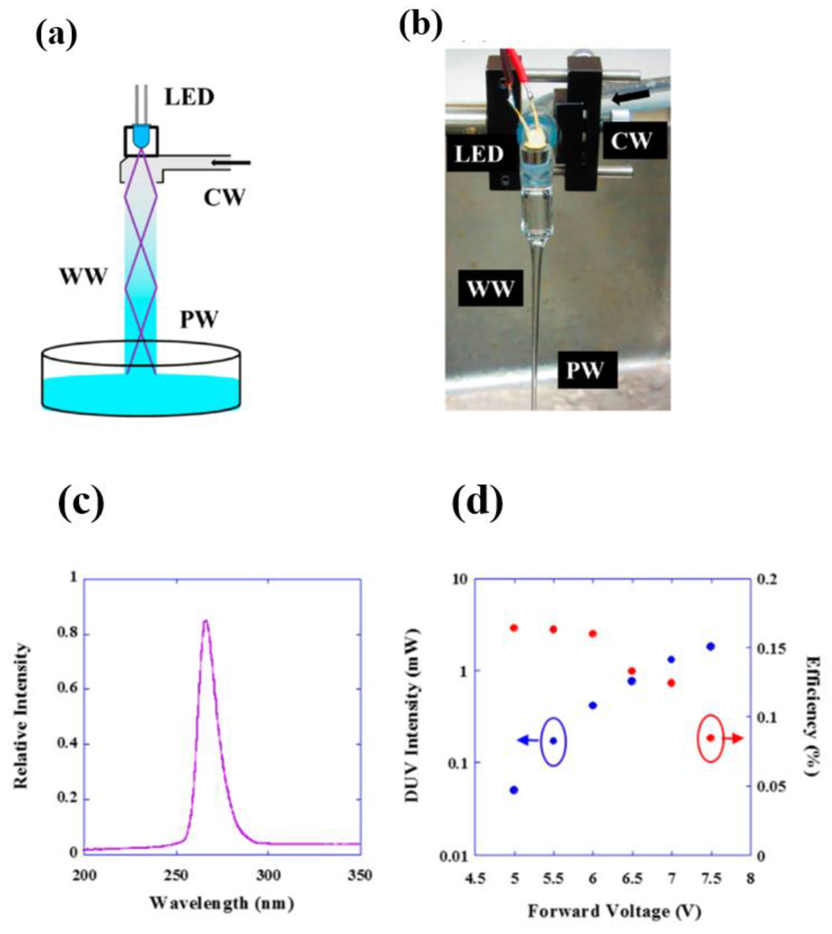
  82. Kang, C.-Y.; Lin, C.-H.; Wu, T.; Lee, P.-T.; Chen, Z.; Kuo, H.-C. A novel liquid packaging structure of deep-ultraviolet light-emitting diodes to enhance the light-extraction efficiency. Crystals 2019, 9, 203. [Google Scholar] [CrossRef] [Green Version]
  83. Ye, Z.T.; Pai, Y.-M.; Lin, C.-H.; Chen, L.-C.; Nguyen, H.T.; Wang, H.-C. Nanoparticle-Doped Polydimethylsiloxane Fluid Enhances the Optical Performance of AlGaN-Based Deep-Ultraviolet Light-Emitting Diodes. Nanoscale Res. Lett. 2019, 14, 1–6. [Google Scholar] [CrossRef]
  84. Chang, M.-H.; Das, D.; Varde, P.; Pecht, M. Light emitting diodes reliability review. Microelectron. Reliab. 2012, 52, 762–782. [Google Scholar] [CrossRef]
  85. Kim, H.-Y.; Lee, J.-W.; Jun, D.-J.; Song, S.-J.; Oh, J.-T.; Jeong, H.-H.; Seong, T.-Y.; Amano, H. Effects of Ultraviolet Wavelength and Ambient Temperature on Reliability of Silicones in InAlGaN-Based Light-Emitting-Diode Package. ECS J. Solid State Sci. Technol. 2020, 9, 035005. [Google Scholar] [CrossRef]
  86. Nagasawa, Y.; Hirano, A. Review of encapsulation materials for AlGaN-based deep-ultraviolet light-emitting diodes. Photonics Res. 2019, 7, B55–B65. [Google Scholar] [CrossRef]
  87. Yasan, A.; McClintock, R.; Mayes, K.; Shiell, D.; Gautero, L.; Darvish, S.; Kung, P.; Razeghi, M. 4.5 mW operation of AlGaN-based 267 nm deep-ultraviolet light-emitting diodes. Appl. Phys. Lett. 2003, 83, 4701–4703. [Google Scholar] [CrossRef]
  88. Stölmacker, C.; Ploch, N.L.; Thies, A.; Hochheim, S.; Rass, J.; Schnieder, F.; Mogilatenko, A.; Ruschel, J.; Kolbe, T.; Knigge, S. Electroplated Gold Microstuds for Thermocompression Bonding of UV LED Chips. IEEE T. Comp. Pack. Man. 2019, 9, 2326–2331. [Google Scholar] [CrossRef]
  89. Shashkov, P.; Khomutov, G.; Yerokhin, A.; Usov, S. Non-Metallic Coating and Method of Its Production. Google Patents WO2012/107754A9, 16 August 2012. [Google Scholar]
  90. Gerchman, Y.; Mamane, H.; Friedman, N.; Mandelboim, M. Corrigendum to” UV-LED disinfection of Coronavirus: Wavelength effect”[Journal of Photochemistry and Photobiology B: Biology 212 (2020) 112044-end page]. J. Photochem. Photobiol. B Biol. 2021, 216, 112132. [Google Scholar] [CrossRef] [PubMed]
  91. Lopez-Malo, A.; Palou, E. Ultraviolet light and food preservation. In Novel Food Processing Technologies; CRC Press: Boca Raton, FL, USA, 2005; pp. 405–422. [Google Scholar]
  92. Rastogi, R.P.; Kumar, A.; Tyagi, M.B.; Sinha, R.P. Molecular mechanisms of ultraviolet radiation-induced DNA damage and repair. J. Nucleic Acids 2010, 2010. [Google Scholar] [CrossRef] [PubMed] [Green Version]
  93. Nyangaresi, P.O.; Qin, Y.; Chen, G.; Zhang, B.; Lu, Y.; Shen, L. Comparison of the performance of pulsed and continuous UVC-LED irradiation in the inactivation of bacteria. Water Res. 2019, 157, 218–227. [Google Scholar] [CrossRef] [PubMed]
  94. Darnell, M.E.; Subbarao, K.; Feinstone, S.M.; Taylor, D.R. Inactivation of the coronavirus that induces severe acute respiratory syndrome, SARS-CoV. J. Virol. Methods 2004, 121, 85–91. [Google Scholar] [CrossRef]
  95. Sholtes, K.A.; Lowe, K.; Walters, G.W.; Sobsey, M.D.; Linden, K.G.; Casanova, L.M. Comparison of ultraviolet light-emitting diodes and low-pressure mercury-arc lamps for disinfection of water. Environ. Technol. 2016, 37, 2183–2188. [Google Scholar] [CrossRef]
  96. Nyangaresi, P.O.; Qin, Y.; Chen, G.; Zhang, B.; Lu, Y.; Shen, L. Comparison of UV-LED photolytic and UV-LED/TiO2 photocatalytic disinfection for Escherichia coli in water. Catal. Today 2019, 335, 200–207. [Google Scholar] [CrossRef]
  97. Nyangaresi, P.O.; Qin, Y.; Chen, G.; Zhang, B.; Lu, Y.; Shen, L. Effects of single and combined UV-LEDs on inactivation and subsequent reactivation of E. coli in water disinfection. Water Res. 2018, 147, 331–341. [Google Scholar] [CrossRef] [PubMed]
  98. Sholtes, K.; Linden, K.G. Pulsed and continuous light UV LED: Microbial inactivation, electrical, and time efficiency. Water Res. 2019, 165, 114965. [Google Scholar] [CrossRef]
  99. Matsumoto, T.; Tatsuno, I.; Hasegawa, T. Instantaneous water purification by deep ultraviolet light in water waveguide: Escherichia coli bacteria disinfection. Water 2019, 11, 968. [Google Scholar] [CrossRef] [Green Version]
  100. Rudnick, S.N.; First, M.W.; Vincent, R.L.; Brickner, P.W. In-place testing of in-duct ultraviolet germicidal irradiation. HVAC&R Res. 2009, 15, 525–535. [Google Scholar]
  101. Yang, Y.; Lai, A.C.; Kong, R.; Deng, Q. Experimental and numerical study of the performance of upper-room ultraviolet germicidal irradiation with the effective Z-value of airborne bacteria. Aerosol Sci. Technol. 2017, 51, 1123–1134. [Google Scholar] [CrossRef] [Green Version]
  102. Yang, Y.; Zhang, H.; Nunayon, S.S.; Chan, V.; Lai, A.C. Disinfection efficacy of ultraviolet germicidal irradiation on airborne bacteria in ventilation ducts. Indoor Air 2018, 28, 806–817. [Google Scholar] [CrossRef]
  103. Zhang, H.; Jin, X.; Nunayon, S.S.; Lai, A.C. Disinfection by in-duct ultraviolet lamps under different environmental conditions in turbulent airflows. Indoor Air 2020, 30, 500–511. [Google Scholar] [CrossRef] [PubMed]
Figure 1. Common UV LED structures separated by fabrication methods.
Photonics 08 00196 g001
Figure 2. EQEs of UV LEDs in spectral range between 200 and 400 nm [7].
Photonics 08 00196 g002
Figure 3. Bottlenecks of DUV-LED chip [16].
Photonics 08 00196 g003
Figure 4. Bright field cross-section TEM images of (a) UV-LEDs with GaN nucleation layer and (b) UV-LEDs with sputtered AlN nucleation layer, g = 0002. S indicates screw dislocation and M indicates mixed dislocation [26].
Photonics 08 00196 g004
Figure 5. Schematic energy band diagrams and hole injection mechanisms for DUV-LED with conventional p-AlGaN EBL [68].
Photonics 08 00196 g005
Figure 6. Mesa surface of DUV chip coated with SiO2/ALD-Al2O3 film for passivation, (a) partial enlarged view of side wall, and (b) mesa cross-section view (c). Comparison of I-V curves of DUV chips with or without ALD-Al2O3 film, and (d) comparison of aging at RT and 60% humidity between DUV chips.
Photonics 08 00196 g006
Figure 7. Bubbles appearing after reliability tests for 32, 105, and 660 h followed by heating up to 230 °C for the p-BVE with –COOH, –COOCH3, and –CF3 end groups, respectively. Reliability tests were conducted using 265-nm LEDs at operation current of 20 mA [86].
Photonics 08 00196 g007
Figure 8. Effect of UV radiation on the infectivity of SARS-CoV [94].
Photonics 08 00196 g008
Figure 9. (a) Schematic diagram and (b) photograph of the water waveguide purification system, (c) emission spectrum of the deep-ultraviolet-LED, and (d) DUV intensity (blue circles) and wall-plug efficiency (WPE) (red circles) versus forward voltage [99].
Photonics 08 00196 g009
Table 1. Summary of applications of UVA, UVB, and UVC LEDs [4].
UVAUVBUVC
Wavelength315–400 nm280–315 nm100–280 nm
Penetration abilityWith strong penetrating power, it can penetrate most transparent glasses and plasticIntermediate penetrating power: shorter-wavelength part will also be absorbed by glassWeak penetration
ApplicationUV radiation therapy, document and banknote, 3D printing, anti-counterfeiting detector, catalyst of light, air purification, medical phototherapyHealth care, plant growthSterilization function, water purification, and air purification
Publisher’s Note: MDPI stays neutral with regard to jurisdictional claims in published maps and institutional affiliations.

