Next Article in Journal
Single Headlamp with Low- and High-Beam Light
Next Article in Special Issue
Inverted p-down Design for High-Speed Photodetectors
Previous Article in Journal
Laser-Induced Thermal Annealing of CH3NH3PbI3 Perovskite Microwires
Previous Article in Special Issue
InP-Components for 100 GBaud Optical Data Center Communication
 
 
Correction published on 23 September 2021, see Photonics 2021, 8(10), 407.
Article

47.5 GHz Membrane-III-V-on-Si Directly Modulated Laser for Sub-pJ/bit 100-Gbps Transmission

by
Nikolaos-Panteleimon (Pandelis) Diamantopoulos
1,*,
Suguru Yamaoka
1,
Takuro Fujii
1,
Hidetaka Nishi
1,
Koji Takeda
1,
Tai Tsuchizawa
1,
Takaaki Kakitsuka
1,2 and
Shinji Matsuo
1
1
NTT Device Technology Labs, NTT Corporation, 3-1 Morinosato Wakamiya, Atsugi, Kanagawa 243-0198, Japan
2
Graduate School of Information, Production and Systems, Waseda University, Kitakyushu-shi, Fukuoka 808-0135, Japan
*
Author to whom correspondence should be addressed.
Photonics 2021, 8(2), 31; https://doi.org/10.3390/photonics8020031
Submission received: 5 January 2021 / Revised: 22 January 2021 / Accepted: 25 January 2021 / Published: 27 January 2021
(This article belongs to the Special Issue Advanced Ultra High Speed Optoelectronic Devices)

Abstract

:
Near-future upgrades of intra data center networks and high-performance computing systems would require optical interconnects capable of operating at beyond 100 Gbps/lane. In order for this evolution to be achieved in a sustainable way, high-speed yet energy-efficient transceivers are in need. Towards this direction we have previously demonstrated directly-modulated lasers (DMLs) capable of operating at 50 Gbps/lane with sub-pJ/bit efficiencies based on our novel membrane-III-V-on-Si technology. However, there exists an inherent tradeoff between modulation speed and power consumption due to the carrier-photon dynamics in DMLs. In this work, we alleviate this tradeoff by introducing photon–photon resonance dynamics in our energy-efficient membrane DMLs-on-Si design and demonstrate a device with a maximum 3-dB bandwidth of 47.5 GHz. This denotes a bandwidth increase of more than 2x times compared to our previous membrane DMLs-on-Si. Moreover, the DML is capable of delivering 60-GBaud PAM-4 signals under Ethernet’s KP4-FEC threshold (net data rate of 113.42 Gbps) over 2-km of standard single-mode fiber transmission. DC energy-efficiencies of 0.17 pJ/bit at 25 °C and 0.34 pJ/bit at 50 °C have been achieved for the > 100-Gbps signals. Deploying such DMLs in an integrated multichannel transceiver should ensure a smooth evolution towards Terabit-class Ethernet links and on-board optics subsystems.

Graphical Abstract

1. Introduction

Operating at the core of most cloud-based applications, intra data center networks (DCNs) and high-performance computing systems (HPC) play an ever-increasing role in the modern ICT ecosystem. Owing to the rapid increase of big-data AI applications and the increasing amount of video content, DCNs and HPCs are required to handle and process a growing amount of data traffic [1]. In order to cope with this traffic growth, future deployments are targeting Terabit-class Ethernet (TbE) links [2] and on-board optics (OBO) subsystems [3], with target data rates exceeding 100 Gbps/lane. Furthermore, for such growth to be accommodated in a sustainable way, high-speed yet energy-efficient optical interconnects based on low-power consumption transceivers are in need. Meanwhile, for economic, environmental, and reliability considerations, such components should be able to operate at temperatures of 50 °C (i.e., “semi-cool” operation) and above (i.e., “un-cool” operation).
Considering the above, low-power consumption directly-modulated lasers (DMLs) [4] are the most energy-efficient solution for transmitters. Further advantages of DMLs compared to externally-modulated transmitters are their low cost and small-size footprint, both of which are crucial for large-scale deployment. Previously, we have demonstrated low-power DMLs based on our novel membrane-III-V-on-Si technology [5,6,7,8]. Owing to such a thin-film (<350 nm thick) InP-based layer buried on SiO2, we can achieve high optical and carrier confinements, which is beneficial both for reducing the power consumption and increasing the modulation speed. Meanwhile, the “on-Si” fabrication allows us to potentially use large Si wafers and existing CMOS processes for further cost reduction, while we have also demonstrated the co-integration of SiOx-based spot-size converters [6] and SiN-based arrayed waveguide grating (AWG) for space- and wavelength-division multiplexing (SDM/WDM) systems [7,8].
The aforementioned membrane DMLs on Si had previously achieved 3-dB bandwidths of around 20 GHz, which enabled us to use them for demonstrating 28 GBaud PAM-4 (56 Gbps) signals with sub-pJ/bit efficiencies [5]. However, due to the intrinsic characteristics of the carrier-photon resonances (CPR) in DMLs, further increases in the modulation speed would require an increase of the bias current of these devices. This effectively translates to an increase of the transmitter’s power consumption, which hinders DMLs’ energy-efficiency capabilities.
Recently, a solution has emerged that effectively alleviates this power-bandwidth tradeoff by introducing detuned-loading (DL) and photon–photon resonance (PPR) effects via specialized longitudinal laser designs [9,10,11,12,13,14,15,16,17]. The DL and PPR effects can be used to effectively boost the high-frequency components of the modulated signal and effectively extend the 3-dB bandwidth of the DML beyond the levels allowed by the intrinsic CPR effect. In particular, in the recent years, two methods have attracted attention to generate these effects: (a) a method based on including a passive feedback waveguide [12,13,14,15,16,17] and (b) a method based on including a distributed Bragg reflector (DBR) [9,10,11,12]. Based on the first method (i.e., passive feedback), we have recently demonstrated DMLs with record-high bandwidths in excess of 100 GHz [17], capable of accommodating net data rates up to 325 Gbps (gross rates > 400 Gbps) [18]. These DMLs were based on our novel membrane-III-V-on-SiC technology, which enabled record-high intrinsic CPR-based 3-dB bandwidths of around 60 GHz, due to the high-thermal conductivity properties of the SiC substrate [17]. Therefore, the bandwidth enhancement due to the DL and PPR effects on such “on-SiC” DMLs was around 1.8x times.
In this paper, we expand on our recently published work [12], in which we demonstrated a bandwidth extension for our membrane DMLs on Si by introducing a DL and PPR-generating longitudinal design based on the DBR method. In particular, a single-mode membrane DML on Si with a maximum 3-dB bandwidth of 47.5 GHz in the O-band was demonstrated, which equals to a bandwidth enhancement of around 2.4x times compared to our previous CPR-based designs [5,6,7]. Moreover, these results pose a ~ 3.9x times improvement in the power consumption compared to similar PPR-based InP DMLs [11] and a significant improvement in terms of both power consumption and 3-dB bandwidth compared to previously demonstrated PPR-based III-V/Si DMLs [15]. In addition, we used this DML to demonstrate 60 GBaud 4-level pulse-amplitude modulated (PAM-4) signals below the Ethernet’s KP4 forward-error correction (KP4-FEC) threshold [19] (i.e., a net rate of 113 Gbps) after 2-km of standard single-mode fiber (SSMF) transmission, with a DC energy-efficiency of 0.17 pJ/bit at a room temperature (RT). Equally important, we further operated the laser at 50 °C to study its eligibility for semi-cool operation in intra-DCNs environments. At this temperature, we were able to demonstrate a similar 60 GBaud PAM-4 (net 113 Gbps) transmission over 2-km of SSMF, with a DC energy-efficiency of 0.34 pJ/bit and a 3-dB bandwidth of 42.5 GHz. Deploying such DMLs in future integrated multichannel transceivers should ensure their suitability for a sustainable evolution towards TbE links and OBO sub-systems.

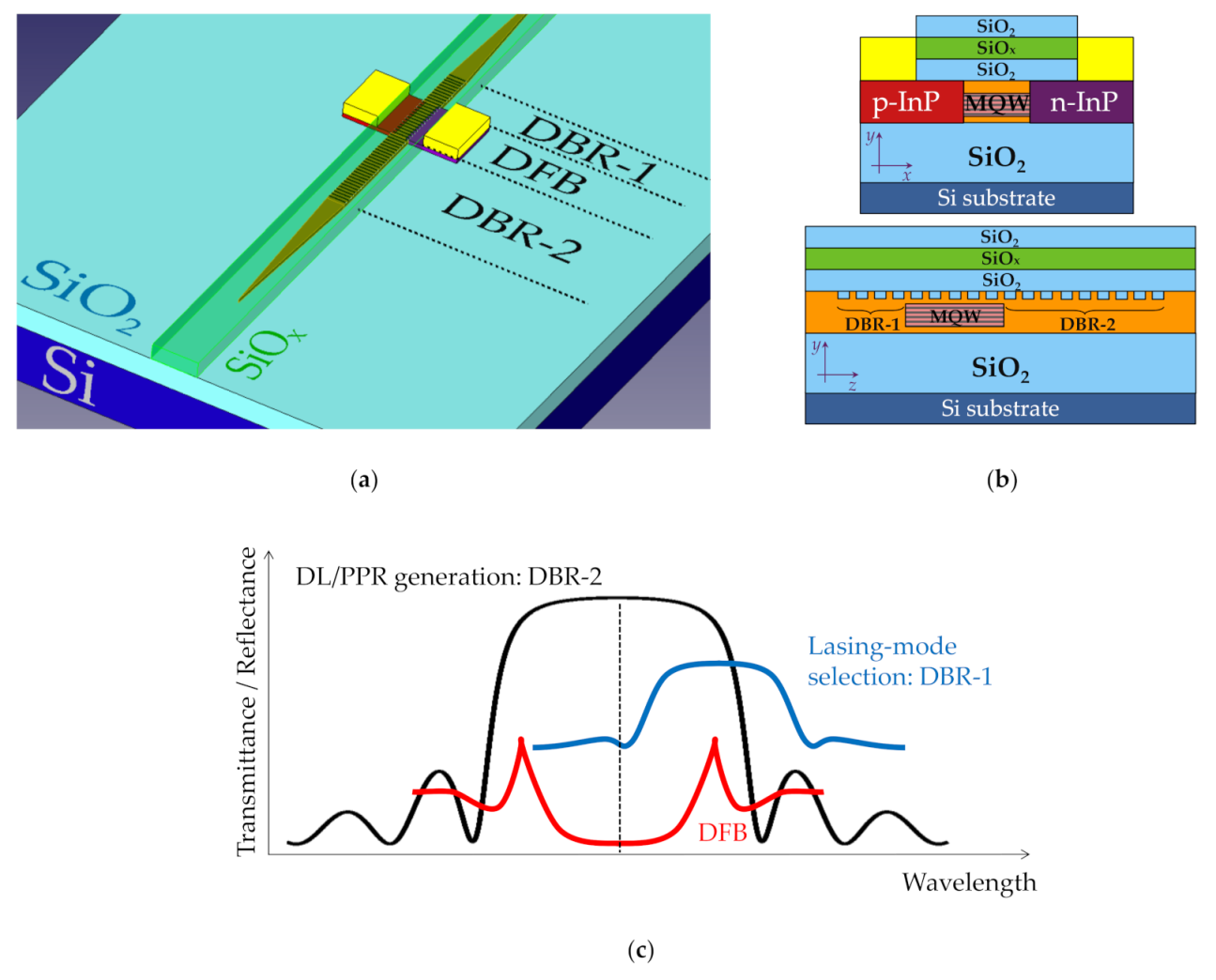
2. Materials and Methods
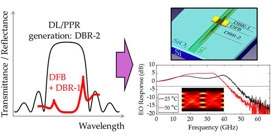
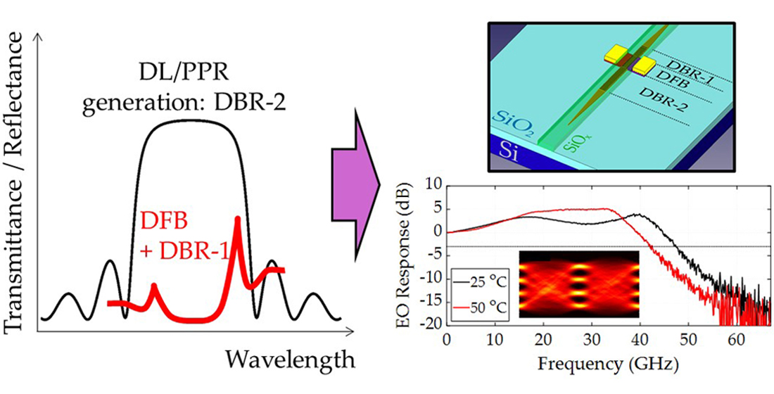
In conventional DMLs, the 3-dB bandwidth and ultimately the modulation speed are widely dependent on the CPR effect, typically given by the relaxation oscillation frequency ( f R ). However, this CPR frequency is proportional to the square-root of the bias current ( I b ) above the threshold current ( I t h ):
f R I b I t h .
In other words, for a DML design with a fixed spatial structure, spatial dimensions, materials, and confinement factor, one can achieve a further increase in the 3-dB bandwidth by increasing the applied bias current. On the other hand, however, the power consumption also increases by increasing the bias current, which leads to a power-bandwidth tradeoff.
As discussed in the introduction, in the recent years, emerging longitudinal cavity designs that enable the DL and PPR effects can alleviate this tradeoff [9,10,11,12,13,14,15,16,17]. In such a case, the DL and/or PPR effects effectively enhance the high-frequency components of the modulated signal, leading to an extension of the 3-dB bandwidths beyond those allowed by pure CPR dynamics.
In more details, the DL effect entails an enhancement on the f R by a factor χ D L [9] such that
f R χ D L · f R .
A sufficient condition for χ D L > 1 and, hence, an enhancement of the 3-dB bandwidth, can be achieved in a longitudinal design that allows for a positive derivative of the mirror loss ( a m ) in respect to wavelength ( λ ) within the vicinity of the lasing wavelength:
χ D L > 1 a m / λ > 0 .
This condition can be satisfied on the long-wavelength side of band-pass filters such as DBRs [9], or Fabry-Perot etalons induced by a passive feedback [16,17].
Unlike the DL effect, the PPR effect does not directly enhance the f R , but rather generates a second resonance frequency in the electro-optic (EO) response of the DML through a photon–photon (i.e., two-mode) interaction. This can also be understood as an optical amplification mechanism of the modulated signal (or, rather, its high-frequency components) via a secondary longitudinal mode. Such PPR frequency ( f P P R ) is proportional to the spectral separation between the main lasing mode and a nearby longitudinal mode ( Δ λ ) via
f P P R = c λ 0 2 Δ λ ,
where c is the speed of light in vacuum and λ 0 is the central wavelength. By carefully designing, therefore, Δ λ in order to obtain a   f P P R a few tens of GHz higher than the intrinsic CPR-based 3-dB bandwidth, one can achieve an increase of more than 2x times in the EO-response bandwidth. One key design consideration, though, is to achieve a relatively flat EO response, void of large dips or valleys between the f R and f P P R , as these would cause a significant penalty on single-carrier modulation formats that typically encompass flat and continuous RF spectra. The PPR and DL can be used in combination, albeit inefficiently, since the DL and PPR optimum spectral positions are typically different. In such a case, a well-designed PPR is usually prioritized for the modulation.
The DBR-based laser design that allowed us to utilize both the DL and PPR effects is shown in Figure 1. The distributed reflector (DR) longitudinal design, shown in Figure 1a, includes a distributed feedback (DFB) section with nonshifted grating, sandwiched between two DBR mirrors with unequal lengths. Similar to our previous works, the shorter, rear DBR (“DBR-1”) section is spectrally detuned compared to the DFB in order to filter one of the two main longitudinal modes present in the DFB’s transmittance spectrum [6]. This is schematically shown in Figure 1c. This design ensures a stable single-mode operation with a large side-mode suppression ratio (SMSR) at a long wavelength and temperature range. However, one should note that the DBR-1 in this case does not contribute to the generation of the DL and PPR effects. Additionally, in this design a second, longer DBR (“DBR-2”) section was also integrated for enabling the DL and PPR effects. In order to use the longer wavelength side of the DBR-2 section for the DL effect, the Bragg wavelength detuning between the DBR-2 and DFB sections was designed to be nearly zero. On the other hand, the Bragg wavelength for the DBR-1 section was designed to be longer than that of the DFB sections in order to filter only the long-wavelength DFB mode, as shown in the schematic of Figure 1c. Moreover, for simplicity the designed grating coupling coefficient for the entire DR structure was kept the same value: 400 cm−1.
For low loss coupling to SSMF, we also integrated SiOx-based spot-size converters on both facets based on 135 μm-long InP tapers, as shown in Figure 1a [6]. In the design presented here, the laser was mainly emitting from the DBR-2-side facet. However, the rear spot-size converter was also integrated in order to evaluate the precise grating profile of DBR-1. Even though is not shown in Figure 1a, the SiOx cores were covered by an SiO2 overcladding. Such a structure was designed to have an output mode field diameter of around 4 μm to match that of high-numerical aperture fibers (HNAFs).
A schematic of the cross-section of the active DFB region is shown in Figure 1b. The structure and its fabrication procedure were based on our established membrane-III-V-on-Si described, e.g., in [5,6]. For the active region, we used 6-period InGaAlAs multiple-quantum wells (MQWs) buried on InP, with a total III-V thickness of ~300 nm. This membrane structure results in a high optical confinement factor, which enhances the f R , while ensuring a low bias current and power consumption. The DFB section was a buried waveguide while the DBR sections were based on InP channel waveguides. For all DFB and DBR sections, the grating was performed by surface etching on top of the InP layer. The grating periods were 219, 226, and 225 nm for the DFB, DBR-1, and DBR-2, respectively. All the gratings were formed on the InP with an etching depth of 20 nm.
For the design and physical simulations of the longitudinal structure we developed an in-house travelling wave (TW) simulator based on the split-step method described in [20]. The main TW equation used is described in the Appendix A, together with the main simulation parameters used. The simulated spectra and the longitudinal mode analysis were based on the same TW model and the methods described in [21] and [22], respectively.

3. Results

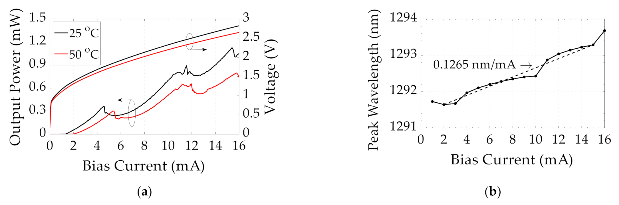
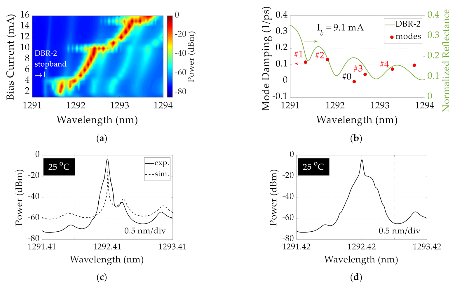
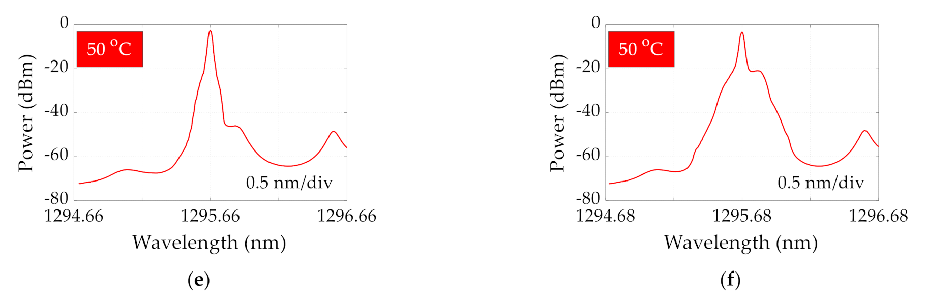
3.1. Laser Characterization

The L-I-V and peak wavelength characteristics of a DML with L D F B = 100 μm, L D B R 1 = 80 μm, and L D B R 2 = 200 μm ( L denotes section lengths here), are shown in Figure 2a,b, respectively. The measurements were performed by a butt-coupled HNAF and the use of an index-matching oil. The fiber-coupling loss was evaluated to be around 3.87 dB. The chip was measured at stage-controlled temperatures of 25 °C and 50 °C. The threshold current for this device was 1.35 mA at 25 °C and 2.0 mA at 50 °C, owing to the membrane structure.
In the L-I curve, three distinct super-linear regions are visible, separated by mode-hoppings. This behavior is commonly observed in DBR-based DMLs exhibiting the DL and PPR effects [11]. This super-linear behavior is explained by an increase in mirror losses while the lasing mode follows the reflectivity slope of the DBR-2 due to the thermal wavelength shift caused by the bias current increase. As shown in Figure 2b, this thermal shift can be linearly fitted with a slope of about 0.127 nm/mA. In the same figure, the mode-hopping is more visible and it is attributed to different DRB-2 side-lobes. Moreover, within the mode-hopping regions, the lasing wavelength follows a nonlinear trend due to the phase change induced by the DBR-2 section in these spectral regions.
The spectral characteristics of the device are summarized in Figure 3. As it can be observed from the contour spectrum plot of Figure 3a, the laser starts lasing in the first long-wavelength-side DBR side-lobe. The simulated longitudinal mode analysis presented in Figure 3b for a bias current of 9.1 mA is used to explain the PPR-generation mechanism. The y-axis of this plot denotes the mode damping [22], which is given by the imaginary part of the mode-eigenfunction solutions of the TW equation corresponding to the mode-gain margin. A negative or close-to-zero mode-damping value corresponds to dominant lasing modes. In this figure, the main lasing mode at the simulated bias current is marked as “#0”, while the first four modes due to the compound-cavity attributed to the DBR-2 section are marked as “#1”, “#2”, “#3”, and “#4”, respectively. Lasing occurs between modes # 1 and # 2 up to the current value at which the first mode hopping occurs, and the lasing mode #0 observes a red-shift afterwards due to the thermal chirp. Therefore, the mode-hoppings observed in the L-I curve are due to the #0 mode coming close to #2, #3, and #4 modes. The optimum PPR conditions are in the spectral vicinity prior to these mode-hoppings.
Figure 3c,e present the simulated and experimentally-obtained static spectra for operations at 25 °C and 50 °C, respectively. The bias currents at these temperatures were 9.1 mA and 15.1 mA, respectively. Based on these spectra, mode separations corresponding to f P P R = 30~40 GHz are obtained. In particular, for the 9.1 mA, 25 °C case of Figure 3c, Δ λ 0.22 nm and f P P R 39.5 GHz. At these bias currents and temperatures, the lasing wavelengths were 1292.41 nm and 1295.66 nm, respectively, as shown in Figure 3c,e. Moreover, the side-mode suppression ratio remained > 40 dB in both cases.
The simulated and experimentally-obtained EO responses for this device are shown in Figure 4a and Figure 4b, respectively. The linewidth was ~5 GHz, which is comparable to previously fabricated devices without PPR. As it can be seen from these results, a 3-dB bandwidth of more than 45 GHz is obtained at RT, with a continuous response between f R and f P P R being above the 3-dB threshold. Moreover, by comparing these results to previous membrane DML-on-Si with a similar structure and without the DBR-2 section (dashed line in Figure 4a) [6], an enhancement of the f R is confirmed owing to the combination of DL and PPR effects. Based on this comparison, the estimated enhancement factor was χ D L 1.4 . As far as the experimentally-obtained data of Figure 4b are concerned, we could achieve flat EO responses of around 47.5 GHz and 42.5 GHz at 25 °C and 50 °C, respectively. At these conditions, the applied bias currents and DC voltages were 9.1 mA and 2.15 V, respectively, at 25 °C, and 15.1 mA and 2.56 V, respectively, at 50 °C. These results translate to DC power consumptions of 19.565 mW at 25 °C and 38.656 mW at 50 °C, and fiber-coupled wall-plug efficiencies of 2.73% and 1.78%, respectively. The wall-plug efficiency using wide-apparatus photodetection without fiber was 6.44% at 25 °C. Moreover, based on these bias currents and Figure 3a–b, at the 9.1 mA/25 °C case, the second long-wavelength side-lobe of the DBR was used (i.e., mode #3 in Figure 3b) for the PPR generation, while for the 15.1 mA/50 °C the third long-wavelength side-lobe of the DBR was used (i.e., mode #4 in Figure 3b) instead.

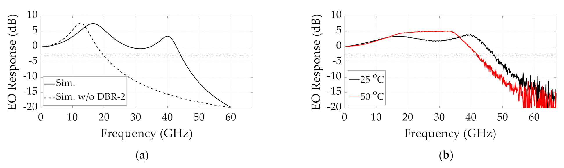
3.2. Evaluation of 60 GBaud PAM-4 Transmission

We evaluated the suitability of our DML for future 100 Gbps/lane systems by performing bit-error rate (BER) measurements of 60 GBaud PAM-4 signals at back-to-back (BTB) and after 2-km SSMF transmissions. A schematic of the experimental setup used for these measurements is illustrated in Figure 5a. The 60 GBaud PAM-4 signals were generated by an arbitrary waveform generator (AWG) at a peak-to-peak modulation bias of 75 mV and with a sampling rate of 120 GSa/s. A root-raised cosine (RRC) filter with a roll-off factor of 22% was used for pulse shaping. Then the RF signal was amplified by a linear RF amplifier with a gain of 22 dB. The fiber coupling was performed by butt-coupling an HNAF, spliced together with a SSMF pigtail, to the chip’s facet. The modulated spectra at 25 °C and 50 °C are shown in Figure 3d,f, respectively. In these figures, the optical amplification effect due to the PPR is observed on the long-wavelength side of the spectrum.
At the receiver side, the opto-electronic conversion was performed by a commercial p-i-n photodiode (PIN), which was integrated together with a trans-impedance amplifier (TIA). The PD’s 3-dB bandwidth was around 32-GHz. Note that no optical amplifier was used in this transmission setup. After the photodetection, the signals were stored by a digital sampling oscilloscope (DSO) at a sampling rate of 160 GSa/s for semi-real time offline processing. In the receiver digital signal processing, the signals were first downconverted to 120 GSa/s (2x times 60 GBaud) and correlation-based time synchronization was performed. Then, match filtering was performed by a similar 22% roll-off RRC filter, followed by least-means square adaptive equalization. The digital equalizer was a low-complexity nonlinear filter [23], with 71 linear taps and 51 nonlinear taps, composed of a second and third-order polynomial filter with the addition of only 10 second-order cross-beating terms. The equalized PAM-4 eye diagrams obtained after the 2-km SSMF transmissions, are shown in Figure 5c for 25 °C operation and Figure 5d for 50 °C operation. Distortion-free PAM-4 eye diagrams are observed in both cases.
A summary of the BER performance for different received optical powers (ROPs) is shown in Figure 5b. The illustrated data contain results for both BTB and 2-km SSMF transmissions, and both at 25 °C and 50 °C operations. These measurements were obtained by placing a variable optical attenuator prior to the PIN (not shown in Figure 5a). For all cases a BER below the 400G Ethernet’s standard KP4-FEC threshold [19] was achieved. Considering a 5.8% overhead for such a KP4-FEC implementation, the net rate was around 113.42 Gbps (gross rate: 120 Gbps). Based on this net rate value and the power DC consumptions obtained in the previous subsection, the energy/bit was estimated to be 0.17 pJ/bit at 25 °C and 0.34 pJ/bit at 50 °C case. As a reference, the 7% overhead hard-decision FEC (HD-FEC) threshold [24] is also depicted in Figure 5b. For this HD-FEC threshold, a net rate of around 112.15 Gbps could be achieved with an excess power margin of around 6 dB. This margin can accommodate excess losses caused by WDM/SDM (de-)multiplexers in an integrated multichannel transceiver.

4. Discussion

The 50-GHz-class DML presented in this work can be compared to previous InP-based DML designs that used a similar DBR-based PPR-generation mechanism [11]. Compared to [11], the 3-dB bandwidth presented here was slightly lower (47.5 GHz compared to 55 GHz), but the achieved BER and energy/bit performance for the 60 GBaud PAM-4 signals denotes a higher temperature operation as well as a ~3.9x bias current reduction at RT. In addition, there is no fundamental limitation for our design to achieve 3-dB bandwidths even higher than 55 GHz by further optimizing the longitudinal design. We plan to explore such optimized designs in the future.
Finally, for practical transceiver implementations, our DML design should be expanded to a multichannel array that can support both WDM and SDM multiplexing. For WDM, we have previously demonstrated SiN AWGs integrated with membrane DMLs on Si in [7]. SiN has the advantage of low-loss and small footprint. Furthermore, we have previously demonstrated low-loss and low-crosstalk coupling to multicore fibers based on fiber-based multiplexers [8]. We plan to work on combining these technologies with our new PPR-based DML designs in the future. Moreover, since the detuning mechanism for the PPR for higher temperatures depends only on a bias detuning of a few mA, traditional control electronics can be used for a stable PPR operation over a large temperature range.

5. Conclusions

Intra data center networks and high-performance computing systems are expected to incorporate optical interconnects operating at beyond 100 Gbps/lane in the near future, in order to cope with a rapidly-growing data traffic and processing. To support such a growth with a low-power consumption levels, high-speed transmitters are in need, capable of operating at temperatures of 50 °C and above. However, energy-efficient DML-based transmitters have an inherent power-bandwidth tradeoff that limits their energy-efficiencies at higher modulation speeds.
In this work, by introducing a DBR-based PPR-design on our previously-demonstrated low-power consumption membrane-III-V-on-Si laser platform, we have alleviated this power-bandwidth tradeoff, and have demonstrated > 100 Gbps PAM-4 signals over 2-km transmissions with 0.17 pJ/bit at 25 °C and 0.34 pJ/bit at 50 °C. Deploying such DMLs in an integrated multichannel transceiver should ensure a smooth evolution towards Terabit-class Ethernet links and on-board optics subsystems.

Author Contributions

Conceptualization, N.-P.D., T.K. and S.M.; methodology, N.-P.D., T.F., K.T., T.T., T.K. and S.M.; software, N.-P.D. and K.T.; validation, N.-P.D. and S.Y.; formal analysis, N.-P.D.; investigation, N.-P.D., S.Y., H.N. and K.T.; resources, S.M.; data curation, N.-P.D.; writing—original draft preparation, N.-P.D.; writing—review and editing, N.-P.D., T.K. and S.M.; visualization, N.-P.D.; supervision, S.M.; project administration, S.M.; funding acquisition, S.M. All authors have read and agreed to the published version of the manuscript.

Funding

This research received no external funding.

Data Availability Statement

Data available upon reasonable request.

Conflicts of Interest

The authors declare no conflict of interest.

Appendix A

The TW equation used for simulations in this work is given by [9,20,21,22]:
1 v g z t ± z E ± z , t = i β z , t E ± z , t i κ z E z , t ,
where z and t denote the propagation and time axes, respectively, E ± denotes the forward ( + ) and backward ( ) propagating fields, v g denotes group velocity, κ denotes the grating coupling coefficient, and β z , t = δ z + i 2 Γ x y 1 + i α H g z , t a i denotes the longitudinal propagation constant, with δ being the phase detuning factor. A thermally-induced phase change is also included in δ by assuming a thermal shift on the DFB’s Bragg wavelength based on the estimated thermal chirp coefficient. Carrier-induced phase changes are assumed in the definition of the propagation constant through the α H parameter. As is typical with TW modelling [9,20,21,22], boundary conditions were considered at the facets based on the facet reflectivities.
A list of the remaining simulation parameters used and their descriptions is given in Table A1. The parameters are assumed to be uniform in each section. A non-uniform carrier density N z , t is assumed within the DFB section in order to take into account the effect of spatial hole burning. A carrier density rate equation was coupled to Equation (A1) for estimating N z , t dynamically. Furthermore, the effect of gain compression was taken into account in the definition of the gain [8].
Table A1. Simulation parameters used in this work. Additional parameters related to the carrier recombination rate and gain can be found in [8].
SymbolQuantityValue
L D F B DFB section length100 μm
L D B R 1 , L D B R 2 DBR section length80 μm, 200 μm
κ D F B DFB section coupling coefficient400 cm−1 (design), 524 cm−1 (fitting)
κ D B R DBR section coupling coefficient400 cm−1 (design), 405 cm−1 (fitting)
Δ λ 1 Bragg wavelength detuning between DBR-1 and DFB+3.04 nm
a i Internal loss coefficient22 cm−1
Γ x y Filling factor in the MQW active region0.14
α H Linewidth enhancement (Henry) factor2.6
λ / I b Thermal chirp coefficient0.1265 nm/mA
I t h Threshold current1.35 mA
R L , φ L Power and phase of rear-facet reflectivity 11%, 0.7π
η i Internal quantum efficiency40%
1 The front-facet reflectivity was assumed to be negligible.

References

  1. Cisco. Global Cloud Index: Forecast and Methodology; Cisco: San Jose, CA, USA, 2017–2021. [Google Scholar]
  2. Ethernet Alliance. 2020 Ethernet Roadmap. Available online: https://ethernetalliance.org/technology/2020-roadmap/ (accessed on 21 December 2020).
  3. Consortium for On-Board Optics. Optical Connectivity Options for 400 Gbps and Higher On-Board Optics. Available online: https://www.onboardoptics.org/whitepapers (accessed on 21 December 2020).
  4. Matsuo, S.; Kakitsuka, T. Low-operating-energy directly modulated lasers for short-distance optical interconnects. Adv. Opt. Photon 2018, 10, 567–643. [Google Scholar] [CrossRef]
  5. Fujii, T.; Takeda, K.; Nishi, H.; Diamantopoulos, N.-P.; Sato, T.; Kakitsuka, T.; Tsuchizawa, T.; Matsuo, S. Multiwavelength mem-brane laser array using selective area growth on directly bonded InP on SiO2/Si. Optica 2020, 7, 838–846. [Google Scholar] [CrossRef]
  6. Nishi, H.; Fujii, T.; Takeda, K.; Hasebe, K.; Kakitsuka, T.; Tsuchizawa, T.; Yamamoto, T.; Yamada, K.; Matsuo, S. Membrane dis-tributed-reflector laser integrated with SiOx-based spot-size converter on Si substrate. Opt. Express 2016, 24, 18346–18352. [Google Scholar] [CrossRef] [PubMed]
  7. Nishi, H.; Fujii, T.; Diamantopoulos, N.-P.; Takeda, K.; Kanno, E.; Kakitsuka, T.; Tsuchizawa, T.; Fukuda, H.; Matsuo, S. Integration of eight-channel directly modulated membrane-laser array and SiN AWG Multiplexer on Si. J. Light. Technol. 2019, 37, 266–273. [Google Scholar] [CrossRef]
  8. Diamantopoulos, N.-P.; Shikama, K.; Nishi, H.; Fujii, T.; Kishi, T.; Takeda, K.; Abe, Y.; Matsui, T.; Kakitsuka, T.; Fukuda, H.; et al. 400-Gb/s DMT-SDM Transmission based on membrane DML-array-on-silicon. J. Light. Technol. 2018, 37, 1805–1812. [Google Scholar] [CrossRef]
  9. Feiste, U. Optimization of modulation bandwidth in DBR lasers with detuned Bragg reflectors. IEEE J. Quantum Electron. 1998, 34, 2371–2379. [Google Scholar] [CrossRef]
  10. Morthier, G.; Schatz, R.; Kjebon, O. Extended modulation bandwidth of DBR and external cavity lasers by utilizing a cavity resonance for equalization. IEEE J. Quantum Electron. 2000, 36, 1468–1475. [Google Scholar] [CrossRef]
  11. Matsui, Y.; Schatz, R.; Pham, T.; Ling, W.A.; Carey, G.; Daghighian, H.M.; Adams, D.; Sudo, T.; Roxlo, C. 55 GHz Bandwidth Dis-tributed Reflector Laser. J. Lightw. Technol. 2017, 35, 397–403. [Google Scholar] [CrossRef]
  12. Diamantopoulos, N.-P.; Yamaoka, S.; Fujii, T.; Nishi, H.; Takeda, K.; Tsuchizawa, T.; Kakitsuka, T.; Matsuo, S. Net 113-Gbps PAM-4 Transmission using membrane DML-on-Si with 0.34 pJ/bit at 50 °C. In Proceedings of the 46th European Conference on Optical Communication (ECOC 2020), Brussels, Belgium, 6–10 December 2020. Mo2B-4. [Google Scholar]
  13. Radziunas, M.; Glitzky, A.; Bandelow, U.; Wolfrum, M.; Troppenz, U.; Kreissl, J.; Rehbein, W. Improving the modulation bandwidth in semiconductor lasers by passive feedback. IEEE J. Sel. Top. Quantum Electron. 2007, 13, 136–142. [Google Scholar] [CrossRef]
  14. Dalir, H.; Koyama, F. Bandwidth enhancement of single-mode VCSEL with lateral optical feedback of slow light. IEICE Electron. Express 2011, 8, 1075–1081. [Google Scholar] [CrossRef] [Green Version]
  15. Abbasi, A.; Moeneclaey, B.; Verbist, J.; Yin, X.; Bauwelinck, J.; Duan, G.-H.; Roelkens, G.; Morthier, G. Direct and electroabsorption modulation of a III–V-on-silicon dfb laser at 56 GB/S. IEEE J. Sel. Top. Quantum Electron. 2017, 23, 1–7. [Google Scholar] [CrossRef]
  16. Matsui, Y.; Schatz, R.; Che, D.; Khan, F.; Kwakernaak, M.; Sudo, T. Low-chirp isolator-free 65-GHz-bandwidth directly modulated lasers. Nat. Photon. 2021, 15, 59–63. [Google Scholar] [CrossRef]
  17. Yamaoka, S.; Diamantopoulos, N.-P.; Nishi, H.; Nakao, R.; Fujii, T.; Takeda, K.; Hiraki, T.; Tsurugaya, T.; Kanazawa, S.; Tanobe, H.; et al. Directly modulated membrane lasers with 108 GHz bandwidth on a high-thermal-conductivity silicon carbide substrate. Nat. Photon. 2021, 15, 28–35. [Google Scholar] [CrossRef]
  18. Diamantopoulos, N.-P.; Yamazaki, H.; Wakita, H.; Ida, M.; Nosaka, H.; Koyama, F.; Miyamoto, Y.; Matsuo, S.; Yamaoka, S.; Nagatani, M.; et al. >100-ghz bandwidth directly-modulated lasers and adaptive entropy loading for energy-efficient >300-GBPS/Λ IM/DD systems. J. Light. Technol. 2021, 39, 771–778. [Google Scholar] [CrossRef]
  19. IEEE Standard 802.3bs: IEEE Standard for Ethernet-Amendment 10: Media access control parameters, physical layers, and management, parameters for 200 GB/S and 400 GB/S operation. IEEE Std. 2017. [CrossRef]
  20. Kim, B.-S.; Chung, Y.; Lee, J.-S. An efficient split-step time-domain dynamic modeling of DFB/DBR laser diodes. IEEE J. Quantum Electron. 2000, 36, 787–794. [Google Scholar] [CrossRef]
  21. Soda, H.; Imai, H. Analysis of the spectrum behavior below the threshold in DFB lasers. IEEE J. Quantum Electron. 1986, 22, 637–641. [Google Scholar] [CrossRef]
  22. Radziunas, M.; Wünsche, H.-J. Multisection lasers: Longitudinal modes and their dynamics. In Optoelectronic Devices; Piprek, J., Ed.; Springer: New York, NY, USA, 2005; pp. 121–150. [Google Scholar]
  23. Diamantopoulos, N.-P.; Nishi, H.; Kobayashi, W.; Takeda, K.; Kakitsuka, T.; Matsuo, S. On the complexity reduction of the SEC-ond-order volterra nonlinear equalizer for im/Dd systems. J. Lightw. Technol. 2019, 37, 1214–1224. [Google Scholar] [CrossRef]
  24. ITU-T. Recommendation G.975.1: Forward Error Correction for High Bit-Rate DWDM Submarine Systems; ITU: Geneva, Switzerland, 2004. [Google Scholar]
Figure 1. Device schematic: (a) Bird’s eye view of the distributed reflector (DR) laser structure. The overcladding SiO2 layer is omitted for visibility; (b) Cross-sectional view: x-y plane of distributed feedback (DFB) section (top) and y-z plane of entire laser (bottom). The grating was formed on the InP surface; (c) Lasing-mode selection (based on distributed Bragg reflector (DBR)-1) and detuned-loading (DL)+ photon–photon resonance (PPR) generation (based on DBR-2) mechanisms.
Photonics 08 00031 g001
Figure 2. Static characteristics of the laser: (a) L-I-V curves at 25 °C and 50 °C based on fiber-coupled output powers; (b) Peak wavelength versus bias current at 25 °C. The dashed line presents a linear fitting of the thermal chirp coefficient ( λ / I b ).
Photonics 08 00031 g002
Figure 3. Spectral characteristics: (a) Contour plot of the experimentally-obtained optical spectra Figure 25 °C; (b) Longitudinal mode analysis at a bias current of 9.1 mA (25 °C operation is assumed). The reflectance of DBR-2 is also shown as a reference. (c) Experimental and simulated spectra at a bias current of 9.1 mA and 25 °C; (d) Experimental spectra as in (c), but including also a 60 GBaud PAM-4 RF modulation. (e) Experimental spectra at a bias current of 15.1 mA and 50 °C; (f) Same as (e), but including also a 60 GBaud PAM-4 RF modulation.
Photonics 08 00031 g003aPhotonics 08 00031 g003b
Figure 4. Normalized laser electro-optic (EO) responses: (a) Simulated using a bias current of 9.1 mA (25 °C operation is assumed). Solid line represents the data of the proposed DML structure, while the dashed line represents the data with the same directly-modulated lasers (DML) structure without including the DBR-2 section; (b) Experimental data at 25 °C and 50 °C, using bias currents of 9.1 mA for the 25 °C operation and 15.1 mA for the 50 °C operation.
Photonics 08 00031 g004
Figure 5. 60 GBaud PAM-4 signal evaluation: (a) Experimental setup; (b) Bit-error rate (BER) versus received optical power at back-to-back (BTB) and after 2-km SSMF transmissions, and (c,d) Eye diagrams after equalization. Measurements were performed at 25 °C ( I b =   9.1 mA) and 50 °C ( I b =   15.1 mA).
Photonics 08 00031 g005
Publisher’s Note: MDPI stays neutral with regard to jurisdictional claims in published maps and institutional affiliations.

