Communication

InP-Components for 100 GBaud Optical Data Center Communication

Fraunhofer Heinrich Hertz Institute (HHI), Einsteinufer 37, 10587 Berlin, Germany
*
Author to whom correspondence should be addressed.
Photonics 2021, 8(1), 18; https://doi.org/10.3390/photonics8010018
Submission received: 16 December 2020 / Revised: 9 January 2021 / Accepted: 11 January 2021 / Published: 13 January 2021
(This article belongs to the Special Issue Advanced Ultra High Speed Optoelectronic Devices)

Abstract

:
Externally modulated DFB lasers (EML) and vertically illuminated photodetectors are presented. Because of their excellent high-speed behavior and operation wavelength of 1310 nm, the devices are of interest for intra-data center communication. Since the EML and the photodetector chips are compatible with current systems, these devices are candidates for upgrading existing transceivers to higher baud rates. Therefore, a proof of concept for 100 GBaud data transmission with the presented components is demonstrated. Even without predistortion, the experiments show clearly open eye diagrams.

Graphical Abstract

1. Introduction

The increasing demand for high data rates for optical data center links has been accomplished with the increase of the symbol rate and a higher modulation order in the recently released transmission standard IEEE 802.3. In many current transceivers, high-performance free-space optics multiplexes the laser output and demultiplexes the CWDM channels into an array of vertically illuminated photodiodes. Transceiver manufacturers tend to upgrade their products by replacing single components but not changing the generic transceiver concept, e.g., when upgrading the symbol rate, only the optoelectronic and electronics are replaced without touching the optics. Additionally, the single components should be compact and allow low-cost production. Therefore, optoelectronic components like high-speed Mach–Zehnder modulators and waveguide integrated photodiodes [1,2,3] are not the first choice when upgrading transceivers due to the larger chip dimensions and the more complex fabrication process above those of the current components.
The first 53 GBaud standardized optical transmission links were commercialized and implemented for intra-data center communication. Recent research publications investigated transmission experiments with direct detection schemes and symbol rates above 100 GBaud [4,5], and also, the industry starts following this trend [6]. The commercial aspects of this trend are to double the data rate without increasing the number of transceivers and thereby keeping the component cost (CapEx) low. However, to our opinion, the operational costs (OpEx) are of greater importance and stronger leverage on the overall costs. In order to keep the OpEx low, low-power consumption is essential. The main power consumers in transmission links are the DSP, e.g., post-compensating with complex algorithms the low component bandwidth [7,8,9].
From the current IEEE 802.3 standard, the required component bandwidth can be approximated with 0.7-times of the targeted symbol rate. For the case of 100 GBaud, this corresponds to a bandwidth of 70 GHz. So far, only a few optoelectronic components have been presented for this symbol rate.
For the transmitters, GaAs-based vertical-cavity surface-emitting lasers (VCSEL) are established light sources at 850 nm wavelength transmission. Some high-speed VCSELs have been demonstrated [10] and even at longer wavelengths in the O-band [11], but VCSELs often suffer from multimode behavior being problematic at high symbol rates due to the mode dispersion. Another low-cost component often used as a short reach transmitter is the directly modulated laser (DML). However, the DML has a limited bandwidth [12] resulting from direct modulation of the light-emitting region with its slow carrier relaxation times. By separating the light generation section from the modulation section with an externally modulated laser (EML) concept, higher bandwidths can be achieved [4,13]. As a further advantage, EMLs generate a smaller chirp than DMLs. Alternative high-speed laser concepts operating with feedback effects in order to increase the modulation bandwidth [14,15] still must verify their applicability under uncooled operation conditions.
On the receiver side, the corresponding devices to the 850 nm VCSELs are GaAs-based photodiodes. These devices are limited by the detection wavelength up to 920 nm. Other potential low-cost candidates for single-mode transmission in the O-band are SiGe-based photodiodes [16] but being limited to a symbol rate of approx. 28 GBaud. InGaAs-based photodiodes have the potential for high-speed performance due to the fast carrier transportation mechanism in the InP-lattice matched material system. Presented InGaAs-based devices so far have suffered from low responsivity and small optical apertures [17,18] and are not applied in the field of data center communication.
In this article, an InP-based electro-absorption EML chip and a vertically illuminated photodetector chip for next-generation 100 GBaud data center transceivers are presented. In the first part of this article, the device characteristics are evaluated. In order to motivate the components for data center applications, the system performance is demonstrated in the second part of the article.

2. Discrete InP-Components

Under the aspect of CapEx, InP components tend to be a bit more expensive in terms of the chip area cost. However, the price per known good die scales with the total number of fabricated components. At the current status, the demand for laser and photodiode dies is still below the numbers needed for silicon devices to pay-off due to the high NRE cost of silicon [19]. Additionally, since last year the first 6-inch InP wafers are commercially available. On one 6-inch wafer, approximately 120,000 laser or photodiode dies can be placed, showing the potential for a further price reduction.

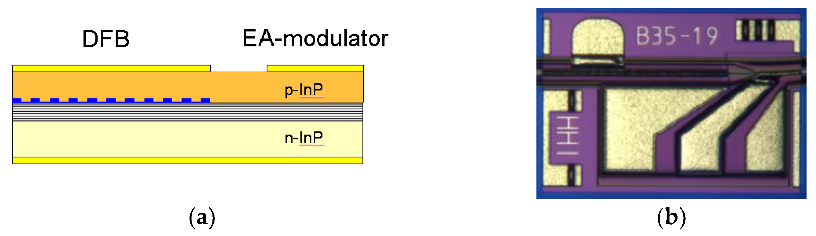
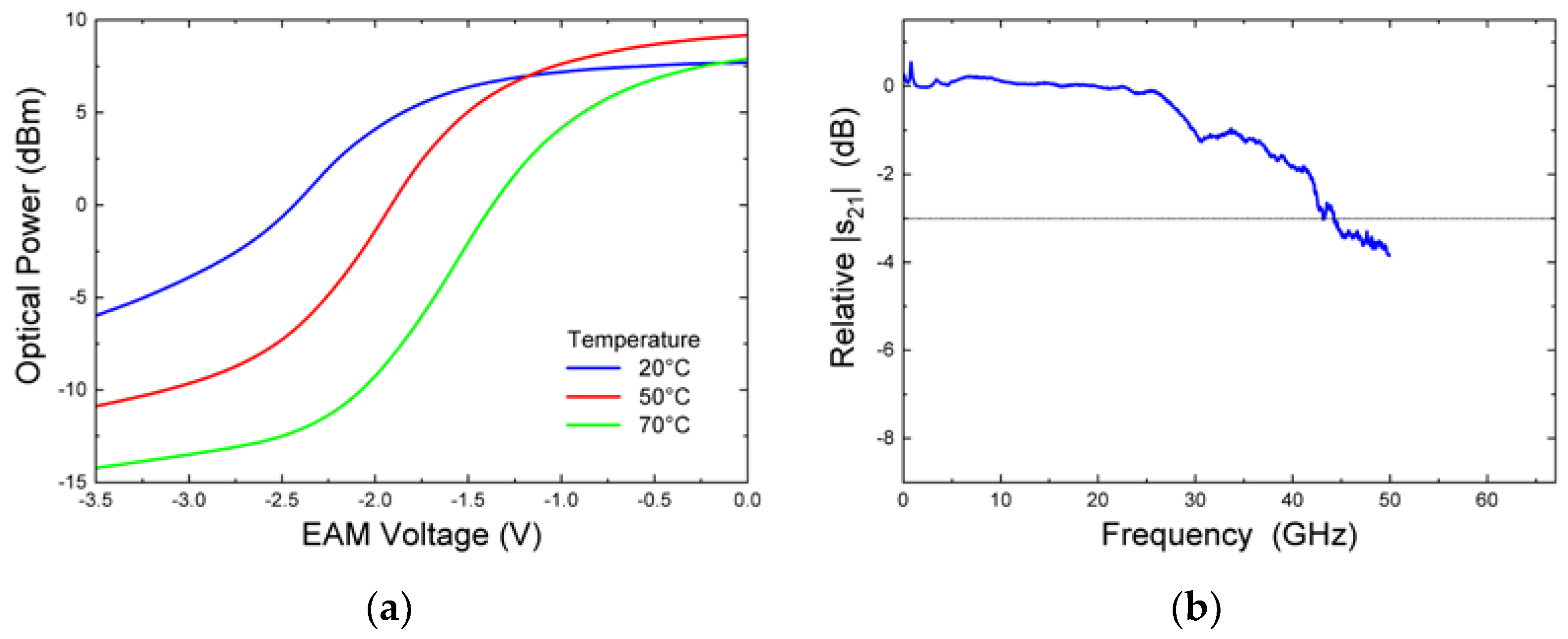
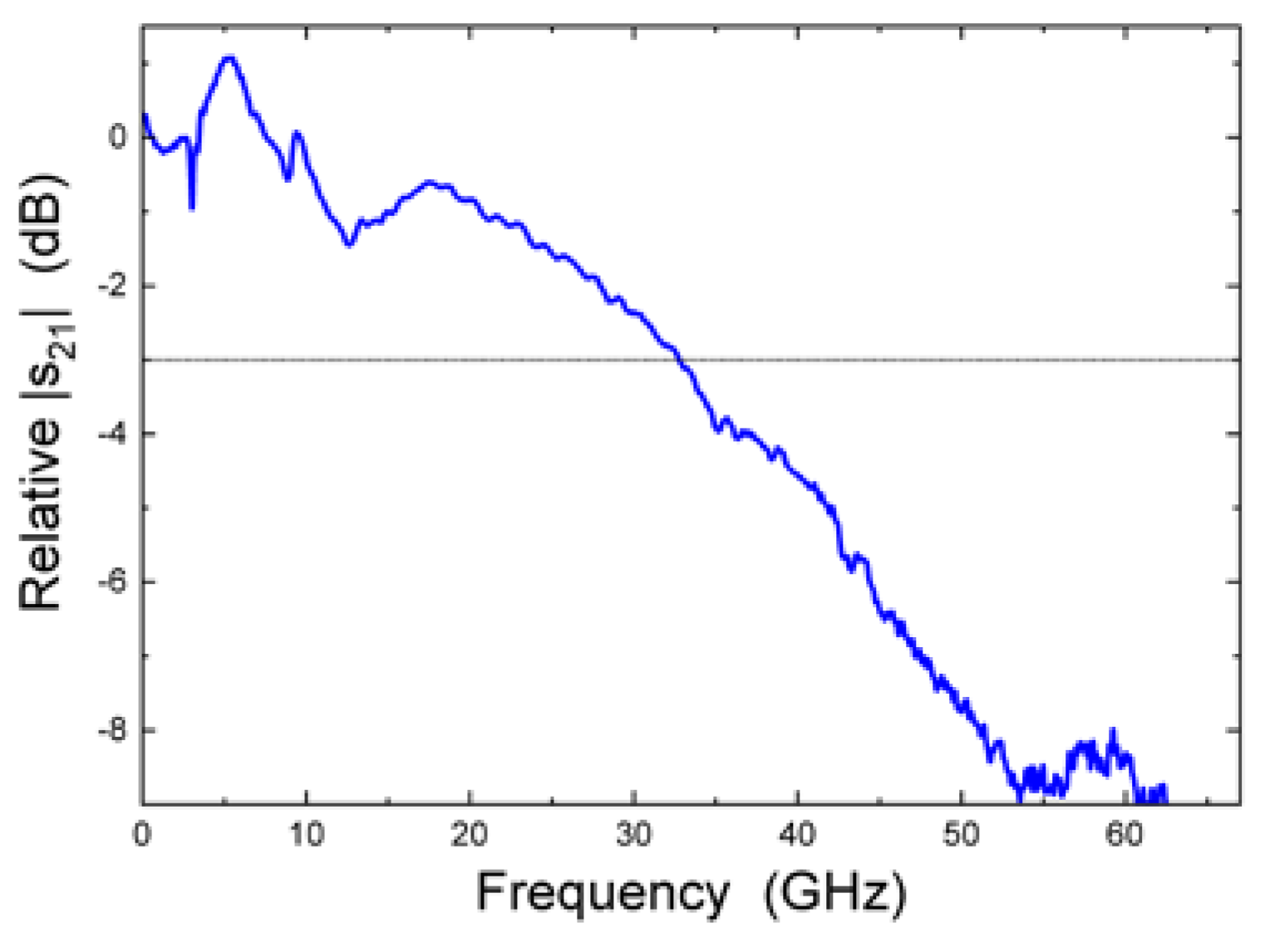
2.1. Electro-Absorption EML

The EML optical transmitter chip consists of an electro-absorption modulator (EAM) and a monolithically integrated distributed feedback laser (DFB) laser (Figure 1a). The structure is based on a ridge waveguide design. With a typical footprint of ~400 µm × ~350 µm, the EML is similar to DMLs. In our case, we used a common active layer concept with an identical InGaAlAs MQW stack for the DFB and the EAM sections. A respective lateral cut of the EML is depicted in Figure 1a. This particular approach allows keeping the processing effort of the EML comparable to that of a DML.
A photograph of the EML chip is shown in Figure 1b. The front facet waveguide has a tilt of 7° in order to minimize optical feedback from front facets into the active regions. The EAM section is 100 µm long. RF contacts to drive the EAM section are realized in a ground–signal–ground configuration. The RF contacts are located on top of the device. An additional pad provides the p-contact of the DFB laser. The n-contact of the laser (common ground with EAM) is accomplished by backside metallization.
The EML performance is illustrated in Figure 2. The static transfer curves of the EAM show the characteristic reduction of output power in fiber with increasing negative bias voltage. Typically, at 50 °C, a high static extinction ratio of > 12 dB can be achieved for voltage difference Vpp = 1.5 V. The figure is further demonstrating the EML operation in a wide temperature range from 20 °C to 70 °C. The modulation response of the EML chip (Figure 2b) shows the high 3 dB-bandwidth of >42 GHz. The RF-data were measured at 50 °C with a chip-level test setup and an impedance-matched RF probe. The high transmitter bandwidth qualifies the compact EML chip for applications at the highest symbol rates.

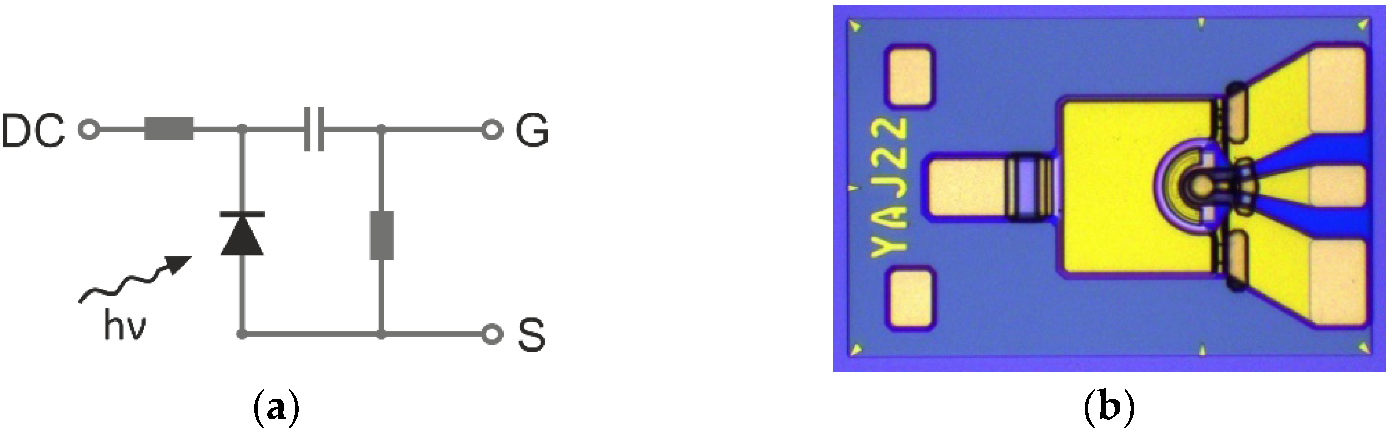
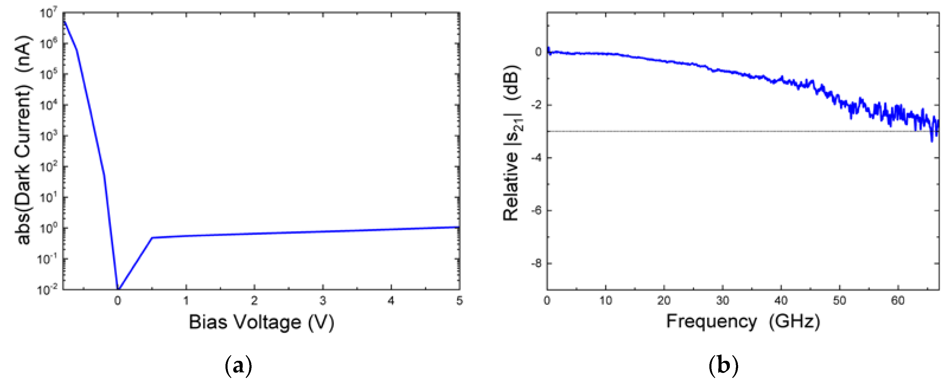
2.2. Vertically Illuminated Photodiode

The photodetector chip is a backside-illuminated photodiode. The chip includes an integrated RC-bias and 50 Ω-termination between the ground and signal at the RF interface (Figure 3a). The photodiode structure is a modified uni-traveling-carrier (MUTC) type photodiode and consists of a highly p-doped wide-bandgap contact, an electron blocking layer, a gradually doped undepleted InGaAs absorbing layer, a second depleted absorbing layer, a lightly n-doped bandgap-graded cliff layer, an InP collection layer, and a heavily n-doped contact layer. Compared to established PIN photodiodes, the carrier transit time in UTC structures is reduced by diffusion of electrons within the p-doped absorbing InGaAs region, where the slower holes as majority carriers experience dielectric relaxation and thus do not limit the bandwidth. The associated reduction of the depletion width, which can limit the RC time constant of the photodiode, is compensated by the InP collection layer. In between the depleted absorber and the collection layer, the slightly n-doped cliff layer minimizes the band discontinuities and controls the electric field strength inside the depleted space charge to realize optimum carrier drift inside [17]. For high 3 dB-bandwidths and RF output powers, the photodiodes RC time constant as well as the carrier transit time needs to be minimized. As described above, for the carrier transit time, only the electrons need to be considered. Additionally, the resulting 3 dB-bandwidth is maximized when the RC bandwidth fRC and the carrier limited bandwidth ft are well balanced for a specific photodiode size. Although waveguide integrated photodiodes can achieve higher bandwidths compared to vertically illuminated photodiodes, vertically illuminated photodiodes allow simpler fabrication processes and smaller chip sizes, resulting in cheaper die costs.
The epitaxial layer structure was grown on a semi-insulating InP substrate using metal-organic chemical vapor deposition followed by deposition of the metal for patterning the p-contact. Standard lithography was adapted for full metallization of the top-contact. Full metallization of the top-contact optimizes the series resistance but also functions as a mirror for the incoming light when illuminating the photodiode from the substrate side and therefore improves the responsivity. Dry etching and wet etching techniques were used to define the mesa. A second etch step was adopted for defining the n-mesa, and consequently, the photodiode mesa was hermetically passivated by SiNx to reduce the carrier recombination at the sidewalls. The n-contact metal was deposited after etching the passivation SiNx. For further improvement of the responsivity, the backside of the chip was anti-reflection coated. A picture of the fabricated photodiode chip is shown in Figure 3b. The photodiode has an optical aperture with a diameter of 14 µm.
In Figure 4, the measurement results of the photodetector chip are presented. In Figure 4a, the dark current of the photodiode is plotted. The performance is especially important for direct detection schemes with PAM-modulation formats because contributing to the SNR. Another important parameter in terms of the SNR is the responsivity of 0.6 A/W for a wavelength of 1310 nm. For the frequency characterization, a network analyzer with calibrated optical frontends was used. The photodetector chip shows a 3 dB-bandwidth of approx. 60 GHz. The large optical aperture and the high responsivity of the photodetector chip are comparable to the performance of current photodiodes in 53 GBaud systems.

3. System Evaluation

The presented components show excellent performance in their characteristics as single devices. In order to demonstrate the capability of the EML and the photodetector chip for 100 GBaud transmission, an experiment is performed.

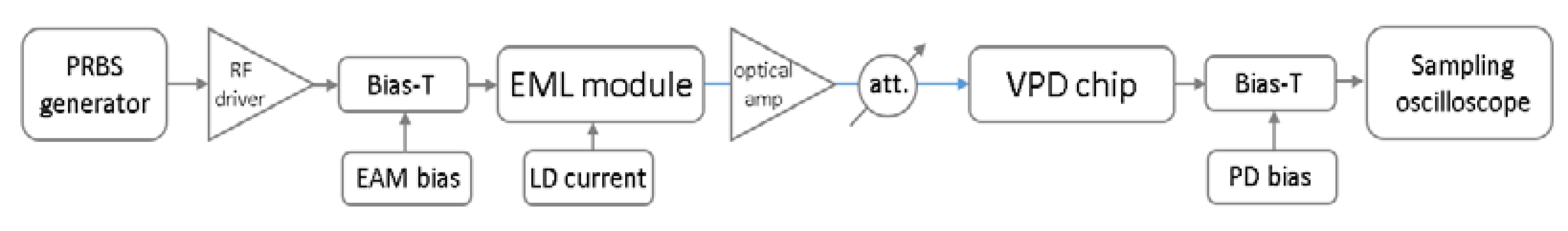
3.1. Experimental Setup

Figure 5 shows the back-to-back transmission setup for the evaluation of the presented devices. One of the main challenges for system evaluation is to reduce the influence of parasitic RF-degradation. When performing measurements in the frequency domain like 3 dB-bandwidth measurements, the influence of the input and output RF cables between DUT and measurement instrument can be de-embedded. In our experimental setup on the transmitter side, the distance between the pseudo random bit sequence (PRBS) generator/RF driver/bias-T and the EML-chip needs to be short. The same holds true for the receiving element, where the distance between the photodetector chip and the bias-T/sampling oscilloscope must be minimized.
Since the attenuation of RF-cables increases at higher frequencies, a sampling oscilloscope with a 70 GHz remote head was used on the receiver side to avoid long RF-cables. On the transmitter side, no remote heads are commercially available. Therefore, when packaging the EML chip into a housing with a 1.85 mm-connector, the assembly is similar to the remote head concept. However, this approach results in a 10 GHz reduction of the 3 dB-bandwidth and a slightly steeper decay of the RF-transmission characteristics (Figure 6), worsening the system performance.
For the system evaluation, the EML was driven at a temperature of 50 °C. The device is designed to show high optical output power and high modulation bandwidth at this temperature in order to allow semi-cooled operation in data centers. The semi-cooled operation will contribute to reduce the power consumption of the thermoelectric cooler inside the transmitter. For the packaged EML chip, the average modulated optical power in the fiber is 4 dBm at 50 °C.

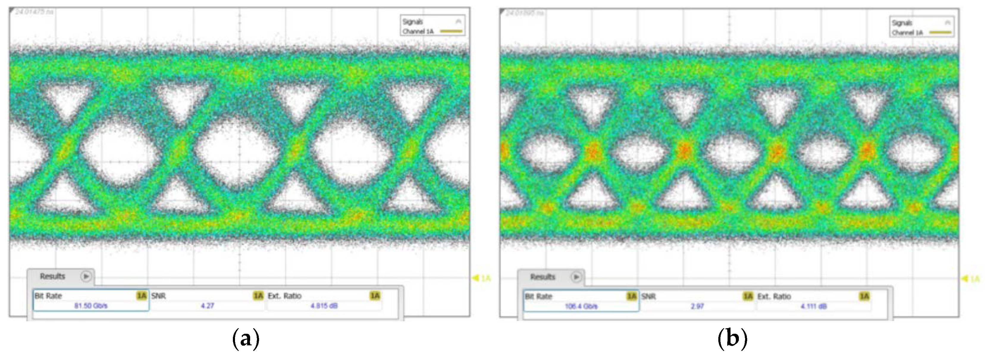
3.2. System Evaluation

Before evaluating the performance of the EML and the photodetector chip as one system, the optical signal generated by the EML module is investigated. Therefore, an optical signal was directly fed into the 60 GHz sampling oscilloscope. From Figure 7, it can be seen that for a symbol rate of 80 GBaud, clearly open error-free eyes can be observed, while for 100 GBaud, the eyes already start to close. We assume that the main contribution of eye closure is caused by the bandwidth reduction of the chip due to the packaging. However, clearly open, almost error-free eyes can be observed, even at 100 GBaud. For the signal generation, no predistortion like peaking from the driver was applied.
For the system measurement, neither predistortion nor post-compensation with DSP-algorithms was applied in order to better evaluate the performance of the single devices. Figure 8 shows the results for the system measurement with the EML and the photodetector chip for different optical input powers. For an optical power of 3 dBm at the photodetector side, open but not error-free eyes are obtained. If the optical input power is increased to 7 dBm, almost error-free transmission at the 100 GBaud is possible. Since no bit error measurements were possible with our measurement setup, the almost bit error-free transmission is derived from almost non-existing sample points around the center-axis in the eye-diagram.

4. Discussion

From Figure 8, it can be seen that the eye closing is mainly related to electrical noise at the receiver side. The optical input power at the receiver is chosen to be slightly higher than in typical data center operations, being only needed in our measurement setup to compensate for electrical losses introduced by the RF-probe head, the bias-T and a short cable, being around 4 dB at higher frequencies. In order to reduce the optical power needed to transmit data, a transimpedance amplifier (TIA) would support lowering the sensitivity level of the receiver part. Although the 50 Ω termination reduces RF output power by 3 dB, a 50 Ω termination was implemented in the photodetector chip in order to improve the detector bandwidth and obtain open eye-diagrams for 100 GBaud transmissions. 100 GBaud data transmission for the same photodetector without 50 Ω termination could not be achieved.
In contrast to the published state of the art EMLs, e.g., [4,13], the presented EML in this article has a common active layer for both the DFB and EAM allowing for a high yield and low-cost device fabrication as only one epitaxial overgrowth step is needed. In spite of this low-cost approach for O-band data center devices, the performance of the device is excellent. A maximum bandwidth exceeding 42 GHz is achieved with lumped EAM electrodes at 50 °C compared to the O-band EML with 59 GHz at 25 °C in [4]. Vpp and optical output power are for both devices very similar. By using shorter EAM sections also bandwidths > 50 GHz are possible. The record 100 GHz bandwidth presented in [13] is achieved with a C-band EML using a traveling-wave (TW) EAM. The drawback of this solution is the larger chip size, the more complex and thus more expensive device fabrication and the lower optical output power. Because of the long EAM section, the output power of such an EML type amounts to 2.5 mW at 100 mA at 22 °C compared to > 4.5 mW at 100 mA at 50 °C for the presented devices. Thus, EMLs with TW EAMs are not suited for high-temperature or uncooled operation in data centers.
In [20], a state-of-the-art vertically illuminated photodetector for 56 GBaud optical transmission links is presented and compared to commercially available devices. All these devices do not exceed a 3 dB-bandwidth of 35 GHz, being insufficient for DSP-free transmission at 100 GBaud. Comparing the device presented in this manuscript to other high-speed vertically illuminated photodiodes [17,18] being suitable for 100 GBaud communication, the presented photodetector chip has a large optical aperture and a high responsivity, making it attractive for data center applications.

5. Conclusions

An InP EML chip and a vertically illuminated photodetector chip for high-speed data transmission at the 1310 nm are presented. Both devices follow the approach of low-cost components for optical intra-data center communication in the O-band. With the devices, a proof of concept for 100 GBaud symbol rate is shown. For later field use, even better performance is expected because the EML and photodetector chips will be hybrid integrated with drivers and TIAs allowing to avoid bulky RF connections as in our setup. Due to co-designed drivers, the power consumption at the transmitter side can be further reduced [21]. Furthermore, if the driver generates an electrically pre-distorted signal for compensating the chirp of the laser, 100 GBaud PAM-4 will be feasible. On the receiver side, the photodetector chip will benefit from TIA, too, because it will increase the receiver sensitivity.
The EML and photodetector chip can be realized in array configurations, allowing further reduction of the assembly cost. While the photodetector can easily cover the entire O-band, an EML-array can cover four of the LAN-WDM wavelengths. Since the high-speed photodiode is a backside illuminated photodetector, a lens integration can be considered to allow simple assembly and efficient light coupling.

Author Contributions

Conceptualization, P.R.; methodology, H.B. and M.G.; investigation, T.B. and U.T.; writing—original draft preparation, P.R.; writing—review and editing, P.R., T.B., U.T., M.G., H.B., M.M. and M.S.; supervision, M.S.; project administration, P.R. and M.M.; funding acquisition, M.S. All authors have read and agreed to the published version of the manuscript.

Funding

This research received no external funding.

Conflicts of Interest

The authors declare no conflict of interest.

References

  1. Ogiso, Y.; Hashizume, Y.; Tanobe, H.; Nunoya, N.; Ida, M.; Miyamoto, Y.; Ishikawa, M.; Ozaki, J.; Ueda, Y.; Wakita, H.; et al. 80-GHz Bandwidth and 1.5-V Vπ InP-Based IQ Modulator. J. Light. Technol. 2019, 38, 249–255. [Google Scholar] [CrossRef]
  2. Sun, S.; He, M.; Xu, M.; Zhang, X.; Ruan, Z.; Zhou, L.; Liu, L.; Liu, L.; Yu, S.; Cai, X. High-Speed Modulator with Integrated Termination Resistor Based on Hybrid Silicon and Lithium Niobate Platform. J. Light. Technol. 2020, 1. [Google Scholar] [CrossRef]
  3. Runge, P.; Zhou, G.; Ganzer, F.; Mutschall, S.; Seeger, A. Waveguide integrated InP-based photodetector for 100 Gbaud applications operating at wavelengths of 1310 nm and 1550 nm. In Proceedings of the 2015 European Conference on Optical Communication (ECOC), Valencia, Spain, 27 September–1 October 2015; pp. 1–3. [Google Scholar]
  4. Kanazawa, S.; Yamazaki, H.; Nakanishi, Y.; Fujisawa, T.; Takahata, K.; Ueda, Y.; Kobayashi, W.; Muramoto, Y.; Ishii, H.; Sanjoh, H. Transmission of 214-Gbit/s 4-PAM signal using an ultra-broadband lumped-electrode EADFB laser module. In Proceedings of the 2016 Optical Fiber Communications Conference and Exhibition (OFC), Anaheim, CA, USA, 20–22 March 2016; pp. 1–3. [Google Scholar]
  5. Yamazaki, H.; Nagatani, M.; Wakita, H.; Nakamura, M.; Kanazawa, S.; Ida, M.; Hashimoto, T.; Nosaka, H.; Miyamoto, Y. 160-GBd (320-Gb/s) PAM4 Transmission Using 97-GHz Bandwidth Analog Multiplexer. IEEE Photonics Technol. Lett. 2018, 30, 1749–1751. [Google Scholar] [CrossRef]
  6. Chang, F. “Source Photonics” OIDA Technology Showcase on Fiber Optics and Communications. 2 December 2020. Available online: https://www.osa.org/en-us/meetings/industry_events/oida_technology_showcase_2020_december/participating_companies/source_photonics/ (accessed on 9 January 2021).
  7. Drenski, T.; Rasmussen, J.C. ADC&DAC—Technology Trends and Steps to Overcome Current Limitations. In Proceedings of the 2018 Optical Fiber Communications Conference and Exposition (OFC), San Diego, CA, USA, 11–15 March 2018; pp. 1–3. [Google Scholar]
  8. Estaran, J.M.; Mardoyan, H.; Jorge, F.; Ozolins, O.; Udalcovs, A.; Konczykowska, A.; Riet, M.; Duval, B.; Nodjiadjim, V.; Dupuy, J.-Y.; et al. 140/180/204-Gbaud OOK Transceiver for Inter- and Intra-Data Center Connectivity. J. Light. Technol. 2018, 37, 178–187. [Google Scholar] [CrossRef]
  9. Heni, W.; Baeuerle, B.; Mardoyan, H.; Jorge, F.; Estaran, J.M.; Konczykowska, A.; Riet, M.; Duval, B.; Nodjiadjim, V.; Goix, M.; et al. Ultra-High-Speed 2:1 Digital Selector and Plasmonic Modulator IM/DD Transmitter Operating at 222 GBaud for Intra-Datacenter Applications. J. Light. Technol. 2020, 38, 2734–2739. [Google Scholar] [CrossRef]
  10. Ledentsov, N.; Chorchos, Ł.; Shchukin, V.; Kalosha, V.; Turkiewicz, J.P. Development of VCSELs and VCSEL-based Links for Data Communication beyond 50 Gb/s. In Proceedings of the 2020 Optical Fiber Communications Conference and Exhibition (OFC), San Diego, CA, USA, 8–12 March 2020; pp. 1–3. [Google Scholar]
  11. Kuchta, D.M.; Huynh, T.N.; Doany, F.E.; Schares, L.; Baks, C.W.; Neumeyr, C.; Daly, A.; Kogel, B.; Rosskopf, J.; Ortsiefer, M. Error-Free 56 Gb/s NRZ Modulation of a 1530-nm VCSEL Link. J. Light. Technol. 2016, 34, 3275–3282. [Google Scholar] [CrossRef]
  12. Wang, W.; Li, H.; Zhang, Z.; Zhao, P.; Zang, D.; Zhu, N.; Lu, Y. Performance Enhancement of 112 Gb/s PAM-4 Amplifier-free 40 km Transmission with record sensitivity Using O-band 25 G-class Directly Modulated Laser. In Proceedings of the 2019 Optical Fiber Communications Conference and Exhibition (OFC), San Diego, CA, USA, 3–7 March 2019; pp. 1–3. [Google Scholar]
  13. Ozolins, O.; Pang, X.; Olmedo, M.I.; Kakkar, A.; Udalcovs, A.; Gaiarin, S.; Navarro, J.R.; Engenhardt, K.M.; Asyngier, T.; Schatz, R.; et al. 100 GHz Externally Modulated Laser for Optical Interconnects. J. Light. Technol. 2017, 35, 1174–1179. [Google Scholar] [CrossRef] [Green Version]
  14. Troppenz, U.; Bornholdt, C.; Kreissl, J.; Rehbein, W.; Sartorius, B.; Schell, M.; Letal, G.; Woods, I. 1.3 µm Passive Feedback Laser for 28 Gb/s and 40 Gb/s transmission over uncompensated SSMF links. In Proceedings of the 2009 35th European Conference on Optical Communication, Vienna, Austria, 20–24 September 2009; pp. 1–2. [Google Scholar]
  15. Yamaoka, S.; Diamantopoulos, N.-P.; Nishi, H.; Nakao, R.; Fujü, T.; Takeda, K.; Hiraki, T.; Kanazawa, S.; Tanobe, H.; Kakitsuka, T.; et al. 239.3-Gbit/s net rate PAM-4 transmission using directly modulated membrane lasers on high-thermal-conductivity SiC. In Proceedings of the 45th European Conference on Optical Communication (ECOC 2019), Dublin, Ireland, 22–26 September 2019; pp. 1–4. [Google Scholar]
  16. Benedikovic, D.; Virot, L.; Aubin, G.; Hartmann, J.M.; Amar, F.; Szelag, B.; Le Roux, X.; Alonso-Ramos, C.; Crozat, P.; Cassan, E.; et al. Silicon-germanium pin photodiodes with double heterojunction: High-speed operation at 10 Gbps and beyond. In Proceedings of the 2020 European Conference on Integrated Optics, Paris, France, 23–25 June 2020. [Google Scholar]
  17. Ito, H.; Kodama, S.; Muramoto, Y.; Furuta, T.; Nagatsuma, T.; Ishibashi, T. High-Speed and High-Output InP-InGaAs Unitraveling-Carrier Photodiodes. IEEE J. Sel. Top. Quantum Electron. 2004, 10, 709–727. [Google Scholar] [CrossRef]
  18. Li, Q.; Li, K.; Fu, Y.; Xie, X.; Yang, Z.; Beling, A.; Campbell, J.C. High-Power Flip-Chip Bonded Photodiode With 110 GHz Bandwidth. J. Light. Technol. 2016, 34, 2139–2144. [Google Scholar] [CrossRef]
  19. Schell, M. InP Solutions for Intra-Datacenter Connects. In Proceedings of the Market Focus European Conference on Optical Communication, Rome, Italy, 24–26 September 2018. [Google Scholar]
  20. Nassem; Chang, H.S.; Chao, R.L.; Huang, J.J.S.; Jan, Y.H.; Chen, H.S.; Ni, C.J.; Chou, E.; Shi, J.W. Uni-Traveling Carrier Photodiodes with Type-II GaAs0.5Sb0.5ZIn0.53Ga0.47As Hybrid Absorbers Integrated with Substrate Lens in 400 Gbit/Sec DR-4 System. In Proceedings of the 2020 Optical Fiber Communications Conference and Exhibition (OFC), San Diego, CA, USA, 8–12 March 2020; pp. 1–3. [Google Scholar]
  21. Choi, J.H.; Gruner, M.; Bach, H.-G.; Theurer, M.A.D.; Troppenz, U.; Möhrle, M.; Schell, M. Ultra-Low Power SiGe Driver-IC for high-speed Electroabsorption Modulated DFB Lasers. In Proceedings of the 2017 Optical Fiber Communications Conference and Exhibition (OFC), Los Angeles, CA, USA, 19–23 March 2017; pp. 1–3. [Google Scholar]
Figure 1. (a) Cross-section of the externally modulated laser (EML) devices with a common active layer stack; (b) top view photograph of the processed EML chip.
Photonics 08 00018 g001
Figure 2. (b) Description of what is (a) static transfer characteristic of the EML at 1310 nm at a DFB current of 80 mA; (b) typical electro-optical response (s21) demonstrating the dynamic transfer characteristic.
Photonics 08 00018 g002
Figure 3. (a) Conceptual scheme of the photodetector chip. The resistor and the capacitor between the DC- and the ground–interface (G) implement the RC bias. The shunt resistor at the RF interface between the signal (S) and the ground (G) is the 50 Ω termination; (b) top view photograph of the processed photodetector chip.
Photonics 08 00018 g003
Figure 4. (a) Dark current of the photodetector chip; (b) RF transmission characteristic for 0 dBm optical input power and −2 V electrical biasing.
Photonics 08 00018 g004
Figure 5. Experimental setup for the system evaluation; following components used: PRBS generator—SHF 12105A, RF drive—SHF M804B, bias-T—SHF BT65R, sampling oscilloscope—Keysight 86118A.
Photonics 08 00018 g005
Figure 6. RF-transmission characteristics of the EML module used in the system evaluation.
Photonics 08 00018 g006
Figure 7. (a) 80 GBaud and (b) 100 GBaud optical eye diagrams of the EML transmitter, measured with the optical input port of the sampling oscilloscope (Keysight 86116C).
Photonics 08 00018 g007
Figure 8. 100 GBaud eye diagram measured at the photodetector chip for the EML transmitter signal as shown in Figure 7b; received optical power of (a) 3 dBm and (a) 7 dBm at a wavelength of 1310 nm.
Photonics 08 00018 g008
Publisher’s Note: MDPI stays neutral with regard to jurisdictional claims in published maps and institutional affiliations.

