1. Introduction
Requirements for photodetectors in optical communications systems are always simple: a larger bandwidth to handle a higher bitrate that will lead to a larger transmission capacity; higher responsivities to extend the transmission distance and allow a larger splitting ratio of optical signals; a lower dark current to ensure reliability and improve the signal-to-noise ratio; and a larger tolerance of assembling. These requirements are elementary but are sometimes a bottleneck limiting the capacity on optical networks. The 400-Gbit/s direct detection system is a good example. The standardization on 400-Gbit/s Ethernet systems limits their transmission ability to 6 km [
1], although past 100- and 200-Gbit/s Ethernet systems have been standardized to reach 10 km using pin photodiodes (pin-PDs). Additionally, discussions on 800-Gbit/s systems for both coherent systems and direct-detection systems are on the horizon, but the outlook is still unclear. There is no doubt that better photodetectors are needed to accelerate such 400- and 800-Gbit/s applications.
Up to now, we have developed high-speed and high-responsivity pin-PDs and avalanche photodiodes (APDs), both with a vertical illumination structure. While the waveguide structure is advantageous to mitigate the tradeoff between responsivity and bandwidth [
2,
3,
4,
5], the vertical illumination structure is still attractive in terms of device fabrication, reliability, and assembly. Particularly, the inverted p-down design we have developed enables the vertical illumination structure to boost bandwidth while maintaining a certain responsivity by incorporating a hybrid absorber consisting of p-type and undoped absorbers while maintaining the benefits of the vertical illumination structure. The inverted p-down design also allows device fabrication using a simple etching process, eliminating ion-implantation or selective diffusion processes for the purpose of confining the active region to the center of the device, which helps further reduce surface leakage.
Here, we review and discuss the design of the inverted p-down structures for pin-PDs and APDs. The inverted p-down APD is designed for high-sensitivity 100-Gbit/s four-level pulse-amplitude modulation (PAM4) operation with a baud rate of 50 Gbaud. The maximum bandwidth reaches 37 GHz and successfully demonstrates 100-Gbit/s PAM4 operation with a receiver sensitivity of −15.5 dBm. The inverted p-down pin-PD with an active diameter of 10 μm exhibits over 70 GHz with 0.61 A/W at 2 V. Even at the bias voltage of 10 V, the dark current is less than 1 nA, which indicates the effectiveness of the inverted p-down design for stabilization on device surfaces.
2. Inverted p-down Design
2.1. Hybrid Absorber
One key consideration to simultaneously achieve a larger responsivity and bandwidth is engineering layer structures to reduce the entire carrier transit time with as thick an absorber as possible. A hybrid absorber is effective for this [
6].
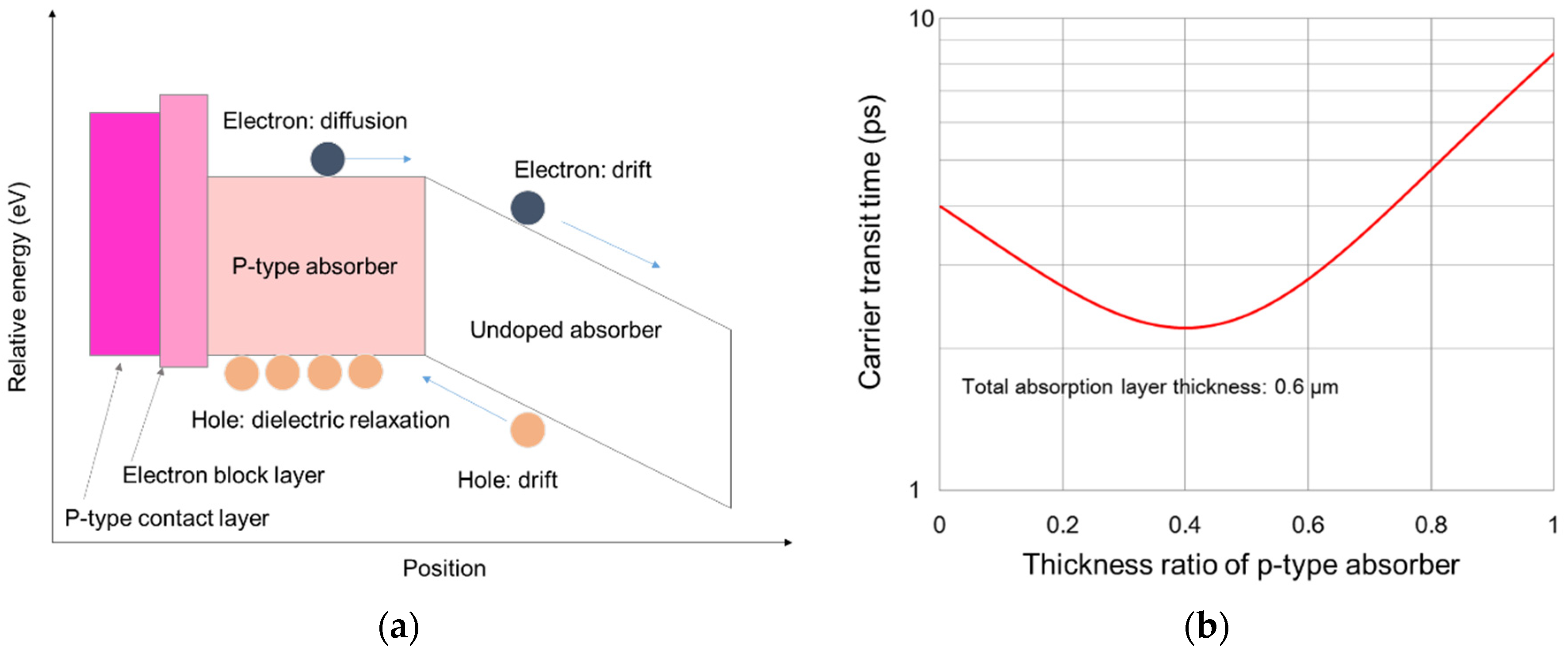
Figure 1a shows a schematic of a hybrid absorber. It consists of a p-type InGaAs absorber at the p-type contact side and an undoped InGaAs absorber at the opposite side. Under the operating bias voltage, the electric field is invoked only in the undoped absorber, while the p-type absorber remains electrically neutral. The electrons generated at the p-type absorber act diffusively with an electron diffusion coefficient of
De. Note that an electron basically moves in both the direction of the p-type contact and its opposite side due to diffusive motion. The electron block layer helps electrons move toward the undoped absorber side. After the electrons are injected into the depleted (undoped) absorber, they drift together with the electrons generated in the undoped absorber. The drift velocity of electrons is governed by the saturation velocity of the electrons in InGaAs. The holes generated in the undoped absorber also are pushed toward the p-type InGaAs absorber by drift. They then behave as a majority carrier in the p-type InGaAs absorber. The electron drift velocity is one digit larger than that of the holes, and the dielectric relaxation time of the hole in the p-type absorber is negligibly smaller compared with other carrier transit times. Thus, in all carrier flows, we can take only electron diffusion and hole drift times into account for considering carrier transit time. Importantly, the responsivity of the hybrid absorber is determined by its total thickness, including its p-type and undoped absorbers. To summarize, the total carrier transit time in a hybrid absorber can be mitigated while maintaining a certain responsivity and, thus, leads to a larger bandwidth.
Figure 1b shows an example of carrier-transit-time behavior against the thickness ratio of the p-type absorber to the entire hybrid absorber. We calculate the carrier transit time based on the charge-control model with a hoe drift velocity of 5.0 × 10
6 cm/s and an electron diffusion coefficient of 2.0 × 10
2 cm
2/s. The thickness ratio of 0 corresponds to a conventional pin absorber and that of 1 corresponds to a uni-traveling carrier (UTC) absorber. Regarding this calculation, we assume a thickness of 600 nm for the entire hybrid absorber. The carrier transit time is at the thickness ratio of 0, mainly governed by the hole saturation velocity and then, the transit time becomes shorter as the thickness ratio enlarges due to the shrinkage of the hole transit distance. Once the transit time reaches the minimum, it increases again due to the enlarged electron drift time. Explained above, the carrier transit time dramatically changes in accordance with this ratio, even though the total thickness is fixed. The minimum carrier transit time of 2.2 ps appears at the ratio of 0.4. The total thickness of the entire hybrid absorber should be set in accordance with the required responsivity; however, the hybrid absorber can reduce the carrier transit time compared with a simple pin or UTC absorber configuration.
2.2. Inverted p-down Design
The vertical illumination structure is beneficial for ensuring reliability because it can be applied to various structures to confine the electric field into a device to avoid device failures owing to surface degradation. Previous studies on avalanche photodiodes (APDs), which require a tighter design to make them reliable, have focused on how to confine the electric field into the central region of the device [
7,
8,
9]. The basic idea for a device structure to confine the electric field in the center of the device is to form a selectively doped region at the undoped layer [
10,
11,
12,
13].
Figure 2a shows a representative APD structure using selective diffusion techniques. The selectively doped p-type contact region in the top undoped layer defines the active region of the device. Thus, the sidewall of the device has no electric field in principle. A similar concept is achieved by the etching process by Levin et al. [
14], as shown in
Figure 2b. They used an etched mesa-form p-type contact layer rather than a p-type selective doping region, eliminating uncertainty in the active region caused by selective diffusion or the ion-implantation process. This concept has been extended to other mesa-type APDs [
15,
16].
When we want to combine a hybrid absorber to boost the operating speed and sensitivity with the vertical illumination structure, however, we have to carefully consider the design. When a hybrid absorber is straightforwardly incorporated into the device configuration shown
Figure 2b, a “terrace” region between the p-type contact layer and absorber will be formed, as shown in
Figure 3. Considering this configuration, the active area is defined not by the p-type contact layer that has a smaller mesa shape, but by the p-type absorber that includes a “terrace” region; thus, the confinement of the electric field is not achievable. This is why our inverted p-down design, which achieves an effective field confinement of a device as well as boosting operation speed and responsivity by introducing a hybrid absorber at the same time, is needed for the vertical illumination structure. Taken from the
Section 3, we present the practical detailed design of inverted p-down pin photodiodes (pin-PDs) and an APD we fabricated and discuss their performance for optical communications.
3. Inverted p-down Pin Photodiodes (Pin-PDs)
The capacity of network systems that require state-of-the-art pin photodiodes (pin-PDs) is now approaching 800 Gbit/s, which uses a baud rate of 100 Gbaud. Studies on such high-speed pin-PDs for 100-Gbaud operation were conducted but used a waveguide structure [
17,
18]. Our approach is developing such high-speed pin-PDs with a vertical illumination structure [
19]. Since the operation voltage and operating electric field of pin-PDs are relatively lower than those of avalanche photodiodes (APDs), the reliability of pin-PDs can be ensured regardless of the device structure. However, the inverted p-down design contributes to extremely low surface leakage of current and tolerance for a larger driving voltage.
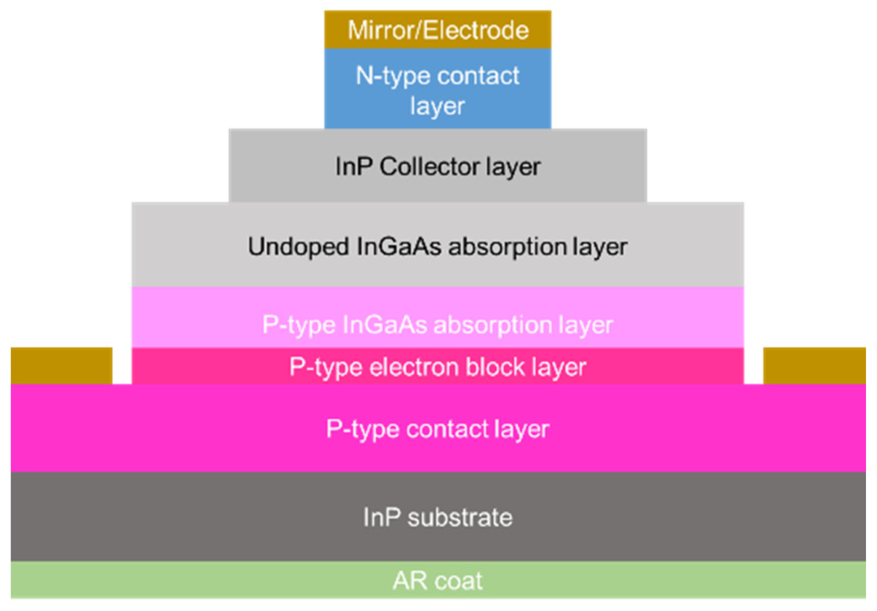
Figure 4 shows a schematic cross-section of one of our inverted p-down pin-PDs.
The layer structure includes a p-type contact layer, a p-type electron block layer, a hybrid absorber consisting of p-type and undoped InGaAs absorbers, an InP collector, and an n-type contact layer, which are placed on top of the InP substrate starting from the p-type contact layer. To obtain a vertical and backside illumination structure, the anti-reflection coat is formed on the backside of the substrate. The mirror on the top reflects the signal light from the bottom side; thus, this structure has a two-path configuration. The active region of the device is defined by the area of the mesa-form n-type contact layer. Since the “terrace” region between the InP collector and n-type contact layer is formed in the undoped layer, strong confinement of the electric field can be achieved.
The thickness of the hybrid absorber is 450 nm, and the thickness ratio of the p-type absorber is set to obtain a maximum bandwidth at the bias voltage around 2–3 V. Compared with a conventional pin absorber, the hybrid absorber shortens the carrier transit time but increases the device capacitance owing to the highly doped p-type absorber. The InP collector layer compensates for the increase in device capacitance. Since only the photo-generated electrons pass through the InP collector, in other words, the InP collector is independent from the behavior of holes that have low drift velocity, the InP collector can extend the entire thickness of the depleted layers, thus reducing device capacitance with a marginal increase in carrier transit time.
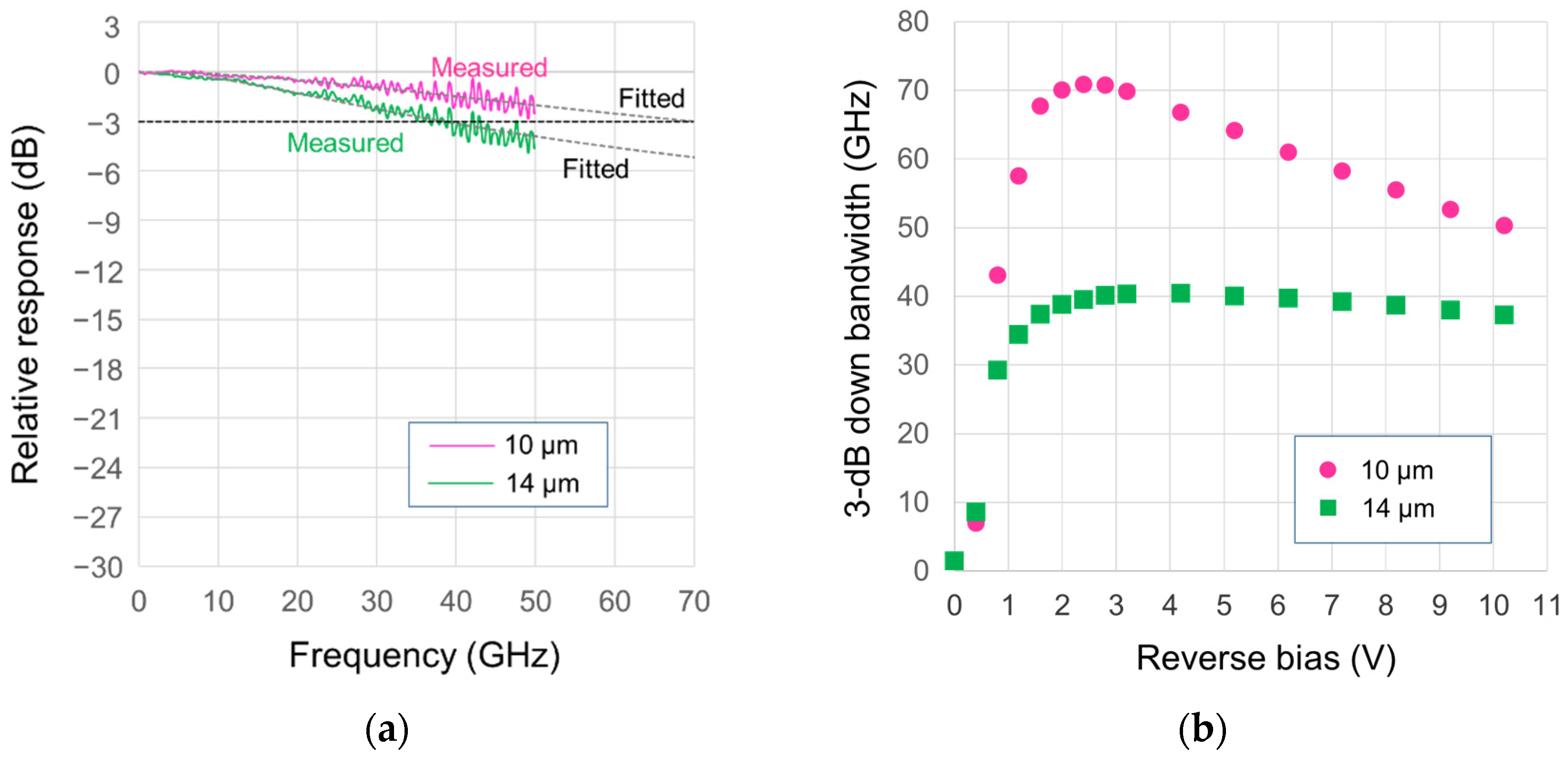
Figure 5a shows the frequency characteristics of our fabricated inverted p-down pin-PDs with active diameters of 10 and 14 μm at 2 V. The 10-μm-diameter pin-PD exhibited a 70.1-GHz bandwidth while the 14-μm-diameter pin-PD exhibited 38.7 GHz. Even with the vertical illumination structure, the 10-μm pin-PD achieved a sufficient bandwidth applicable to 100-Gbaud systems, including 800-Gbit/s networks.
Figure 5b shows the voltage dependence of the bandwidth of these pin-PDs. The 14-μm pin-PD shows a peak bandwidth of 40.4 GHz at 4.2 V and almost completely saturates until the applied bias voltage of 10.2 V. The 10-μm pin-PD exhibited interesting behavior. The bandwidth of this pin-PD initially surges and reaches the peak bandwidth of 70.9 GHz at 2.4 V. It then gradually decreases and finally shrinks to 50.3 GHz at 10.2 V. Note that the device capacitances of each pin-PD should be almost constant once they are fully depleted at the operating voltage. It is reasonable if we assume that the carrier transit time increases due to lowering electron velocity in accordance with the additional bias, and the 10-μm pin-PD well reflect the delay in the transit time while the bandwidth of the 14-μm pin-PD is governed by the capacitance-resistance time constant.
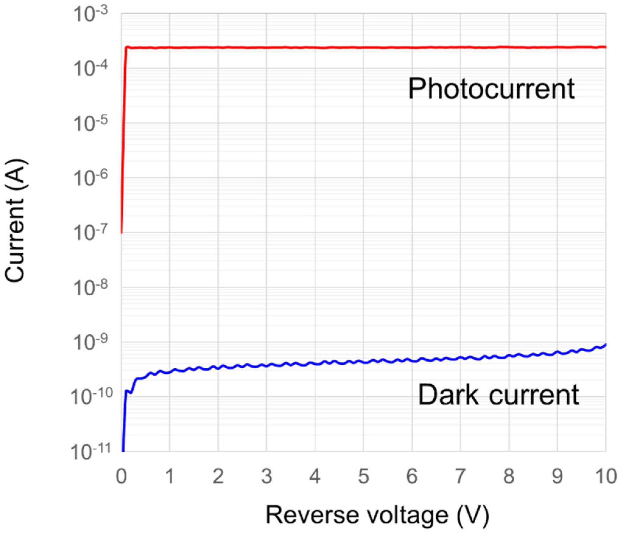
Figure 6 shows the current-voltage (I-V) characteristics of the 10-μm pin-PD. The input is a 1.3-μm wavelength and a −4-dBm power. Thanks to the inverted p-down design, the dark current is maintained at less than 1 nA for bias voltage up to 10 V. Judging from the observed photocurrent, the responsivity is 0.61 A/W. Thus, the 10-μm pin-PD exhibited 0.61 A/W with a bandwidth of over 70 GHz simultaneously, even with the vertical illumination structure. It is interesting that the photocurrent remains the same until 10 V, indicating that avalanche multiplication still does not occur for the entire voltage region. This result also indicates that the gradual decrease in the bandwidth for additional bias voltage is independent of avalanche multiplication, seemingly due to the lowering of electron velocity.
4. Inverted p-down Avalanche Photodiodes (APDs)
While the pin photodiodes (pin-PDs) were designed to achieve 100-Gbaud operation, cutting-edge avalanche photodiodes (APDs) are being designed for 100G- four-level pulse-amplitude modulation (PAM4) (50 Gbaud) operation with a higher sensitivity to reach over a 10-km transmission [
20,
21].
Figure 7a shows a schematic cross-section of our fabricated inverted p-down APD. Compared with the inverted p-down pin-PDs, the epitaxial structure becomes more complex. The layer structure includes a p-type contact layer, p-type electron block layer, a hybrid absorber consisting of p-type and undoped InGaAs absorbers, a 90-nm-thick InAlAs avalanche layer sandwiched between n-type and p-type field control layers, an InP edge-field buffer layer, and an n-type contact layer.
The thickness of the hybrid absorber is 500 nm. Seen from the pin-PDs discussed in the
Section 3, the inverted p-down design efficiently decreases the surface leakage current. However, we also have to consider the electric field of the internal region in the case of an APD. A bias voltage as large as 30 V needs to be applied to this APD, and the electric field in each layer reaches several hundred kV/cm, unlike in pin-PDs. During such a situation, the edge field invoked in the edge region of each mesa can be problematic. Particularly, if the edge field reaches the avalanche layer, avalanche multiplication will be enhanced at the local region, leading to an abnormal breakdown. The edge-field buffer layer helps mitigate this. The edge-field buffer layer separates the avalanche layer and n-type contact layer spatially, weakening the edge field by the n-type contact layer at the avalanche layer. The edge-field buffer layer also is exposed to the edge field; however, the n-type field-control layer lowers the electric field in the edge-field buffer layer, as shown in
Figure 7b.
Figure 7b is the electric field profile of the APD under the gain condition of around 5.
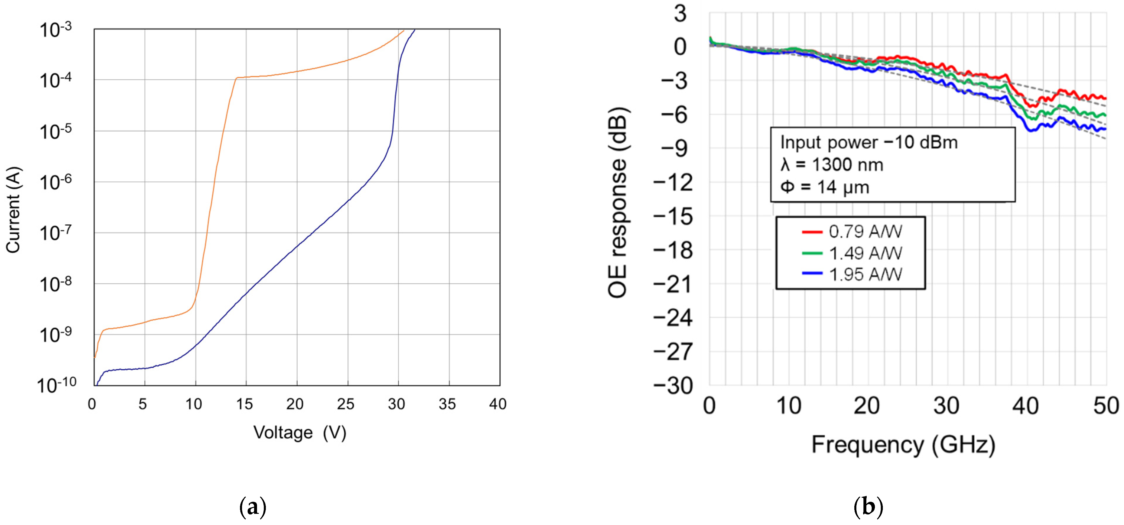
Figure 8a shows the current-voltage (I-V) characteristics of our fabricated inverted p-down APD with a 14-μm active diameter. We can find no abnormal breakdown. After the on-set voltage of 14.5 V, the photocurrent gradually increases according to the avalanche gain, then reaches break down at 30 V.
Figure 8b shows the frequency response of this APD. The peak bandwidth of 37 GHz appears at 0.79 A/W at a 1.3-μm-wavelength input. While the responsivity increases according to the increase in the avalanche gain, the bandwidth gradually decreases. However, a bandwidth of over 28 GHz, which is sufficient to operate at 100-Gbit/s PAM4, is maintained at a responsivity of 1.95 A/W.
We mounted this APD onto an optical receiver together with a commercially available trans-impedance amplifier and conducted a bit-error-ratio (BER) measurement to confirm the capability of the APD to handle a 100-Gbit/s PAM4 optical signal. We used our in-house semiconductor optical amplifier assisted extended reach electro-absorption modulator integrated with distributed feedback laser (AXEL) with a wavelength of 1294.82 nm and an average launch power of +8.4 dBm as a transmitter [
22]. A commercially available digital signal processor was connected to the transmitter and receiver to measure receiver sensitivity at a BER of 2.4 × 10
−4, which corresponds to the error-free condition assuming KP-4 forward error corrector (FEC).
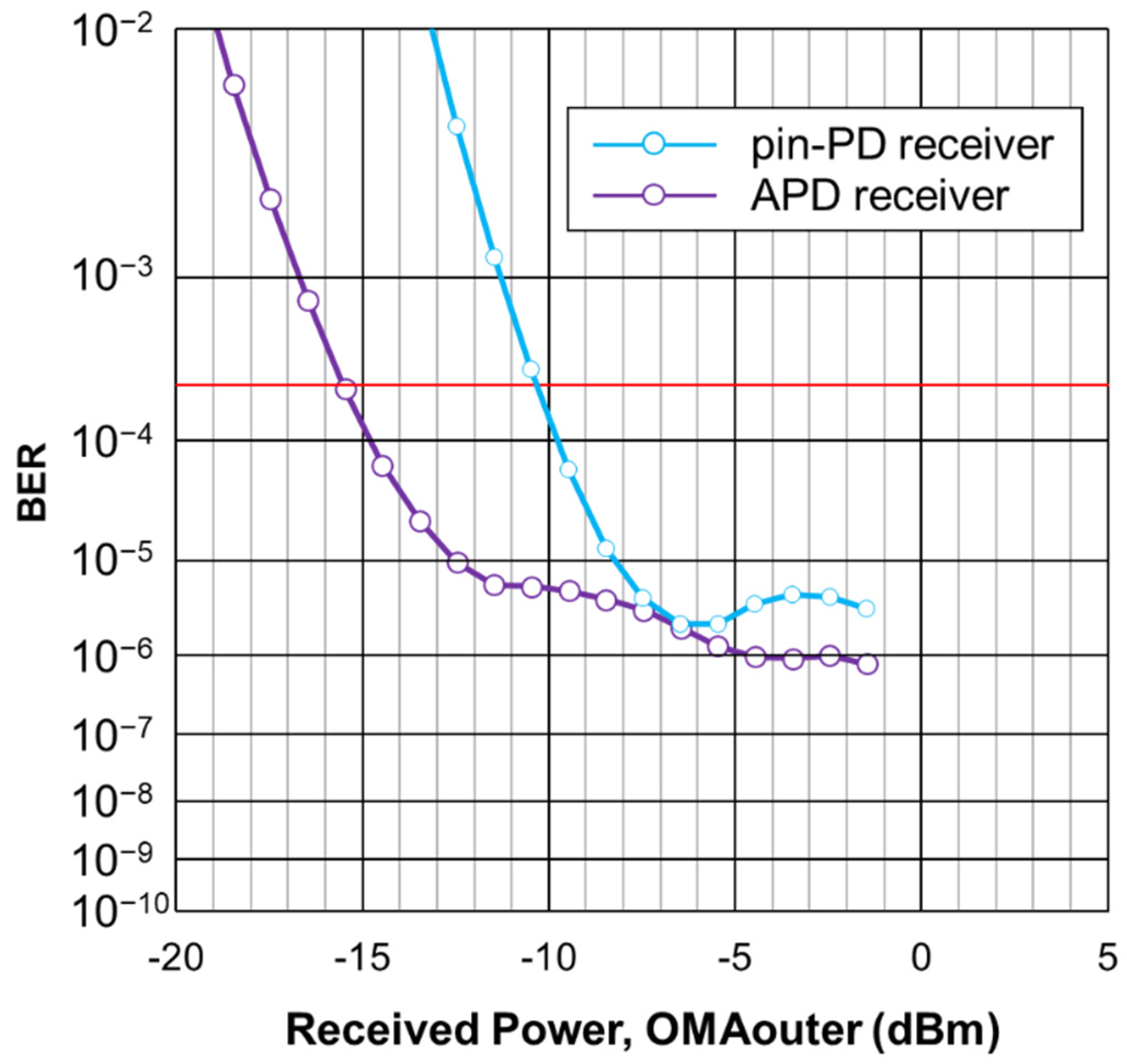
Figure 9 shows the BER characteristics. A minimum receiver sensitivity of −15.5 dBm in the outer optical modulation amplitude (OMA outer) was achieved at the APD gain of 5 for a 100-Gbit/s PAM4 optical signal. The BER characteristics of the optical receiver with a pin-PD also is shown in this figure. Compared with the receiver sensitivity of the pin-PD receiver of −10.3 dBm, the APD receiver exhibited a 5.2-dB improvement.
5. Conclusions
We reviewed the design and benefits of the inverted p-down structure for photodetectors and discussed their performance. The inverted p-down design allowed the incorporation of a hybrid absorber to a mesa-type configuration that confined the electric field into the center of the device. The incorporation of a hybrid absorber resulted in an over 70-GHz bandwidth and a 0.61-A/W responsivity with a 10-μm pin photodiode (pin-PD), even with the vertical illumination structure, while the field confinement that the mesa-type configuration provided contributed to an extremely low dark current of less than 1 nA, even at 10 V. The inverted p-down avalanche photodiodes (APD) also included a hybrid absorber. A responsivity of 1.95 A/W was obtained at over 28 GHz, which was sufficient bandwidth to handle a 100-Gbit/s four-level pulse-amplitude modulation (PAM4) signal. The optical receiver fabricated with this APD exhibited a −15.5-dBm sensitivity.
Author Contributions
Conceptualization, M.N.; methodology, M.N., F.N., A.K., T.Y., Y.N., S.T. and T.S.; investigation, M.N., F.N., A.K., T.Y., Y.N., S.T. and T.S.; writing—original draft preparation, M.N.; writing—review and editing, all authors; supervision, H.M. and K.S.; project administration, H.M. and K.S. All authors have read and agreed to the published version of the manuscript.
Funding
This research received no external funding.
Institutional Review Board Statement
Not applicable.
Informed Consent Statement
Not applicable.
Data Availability Statement
Not applicable.
Conflicts of Interest
The authors declare no conflict of interest.
References
- IEEE P802.3cu 100 Gb/s and 400 Gb/s over SMF at 100 Gb/s per Wavelength Task Force. Available online: http://www.ieee802.org/3/cu/index.html (accessed on 4 January 2021).
- Runge, P.; Zhou, G.; Beckerwerth, T.; Ganzer, F.; Keyvaninia, S.; Seifert, S.; Ebert, W.; Mutschall, S.; Serger, A.; Schell, M. Waveguide Integrated Balanced Photodetectors for Coherent Receivers. IEEE J. Sel. Top. Quantum Electron. 2017, 24, 6100307. [Google Scholar] [CrossRef]
- Beling, A.; Campbell, J. InP-based high-speed photodetectors. J. Lightwave Technol. 2009, 27, 343–355. [Google Scholar] [CrossRef]
- Beling, A.; Campbell, J. High-speed photodiodes. J. Sel. Top. Quantum Electron. 2014, 20, 3804507. [Google Scholar] [CrossRef]
- Shi, J.W.; Wu, Y.S.; Wu, C.Y.; Chiu, P.H.; Hong, C.C. High-speed, high-responsivity, and high-power performance of near-ballistic uni-traveling-carrier photodiode at 1.55 μm wavelength. IEEE Photon. Tech. Lett. 2005, 17, 1929–1931. [Google Scholar] [CrossRef]
- Muramoto, Y.; Ishibashi, T. InP/InGaAs pin photodiode structure maximizing bandwidth and efficiency. Electron. Lett. 2003, 39, 1749–1750. [Google Scholar] [CrossRef]
- Watanabe, I.; Tsuji, M.; Hayashi, M.; Makita, K.; Taguchi, K. Reliability of mesa-structure InAlGaAs/InAlAs superlattice avalanche photodiodes. IEEE Photon. Technol. Lett. 1996, 8, 824–826. [Google Scholar] [CrossRef]
- Sudo, H.; Suzuki, M.; Miyahara, N. Observation of the surface degradation mode of InP/InGaAs APD’s during bias-temperature test. IEEE Electron. Device Lett. 1987, 8, 386–388. [Google Scholar] [CrossRef]
- Sudo, H.; Suzuki, M. Surface degradation mechanism of InP/InGaAs APDs. J. Lightwave Technol. 1988, 6, 1496–1501. [Google Scholar] [CrossRef]
- Yagyu, E.; Ishimura, E.; Nakaji, Y.; Aoyagi, T.; Tokuda, Y. Simple planer structure for high-performance AlInAs avalanche photodiodes. IEEE Photon. Technol. Lett. 2006, 18, 76–78. [Google Scholar] [CrossRef]
- Ishimura, E.; Yagyu, E.; Nakaji, M.; Ihara, S.; Yoshihara, K.; Aoyagi, T.; Tokuda, Y.; Ishikawa, T. Degradation mode analysis on highly-reliable guardring-free planer AlInAs avalanche photodiodes. J. Lightwave Technol. 2007, 25, 3686–3693. [Google Scholar] [CrossRef]
- Liu, Y.; Forrest, S.R.; Hladky, J.; Lange, M.J.; Olsen, G.H.; Ackley, D.E. A planer InP/InGaAs avalanche photodiode with floating guard ring and double diffused junction. J. Lightwave Technol. 1992, 10, 182–193. [Google Scholar] [CrossRef]
- Tarof, L.E.; Bruce, R.; Knight, D.G.; Yu, J.; Kim, H.B.; Baird, T. Planer InP-InGaAs single-growth avalanche photodiode with no guard rings. IEEE Photon. Technol. Lett. 1995, 7, 1330–1332. [Google Scholar] [CrossRef]
- Levine, B.F.; Sacks, R.N.; Ko, J.; Jazwiecki, M.; Valdmanis, J.A.; Gunther, D.; Meier, J.H. A new planer InGaAs-InAlAs avalanche photodiode. IEEE Photon. Technol. Lett. 2006, 18, 1898–1900. [Google Scholar] [CrossRef]
- Wu, S.L.; Wun, J.M.; Chao, R.L.; Huang, J.; Wang, N.; Jan, Y.H.; Chen, H.S.; Ni, C.J.; Chang, H.S.; Chou, E.; et al. High-speed InAlAs based avalanche photodiode with top-illuminated design for 100 Gb/s ER-4 system. J. Lightwave Technol. 2018, 36, 5505–5510. [Google Scholar] [CrossRef]
- Zhao, H.Y.; Jones, A.H.; Chao, R.L.; Ahmad, Z.; Campbell, J.C.; Shi, J.W. High-speed avalanche photodiodes with wide dynamic range performance. J. Lightwave Technol. 2019, 37, 5945–5952. [Google Scholar] [CrossRef]
- Runge, P.; Zhou, G.; Ganzer, F.; Schell, M.; Seeger, A. Waveguide integrated InP-based photodetector for 100Gbaud applications operating at wavelengths of 1310 nm and 1550 nm. In Proceedings of the European Conference on Optical Communication, Valencia, Spain, 17 September–1 October 2015. [Google Scholar]
- Runge, P.; Zhou, G.; Ganzer, F.; Seifert, S.; Mutschall, S.; Seeger, A. Polarisation Insensitive Coherent Receiver PIC for 100Gbaud Communication. In Proceedings of the Optical Fiber Communication Conference and Exhibition, Anaheim, CA, USA, 22–24 March 2016. [Google Scholar]
- Nada, M.; Nakajima, F.; Tatsumi, S.; Yamada, Y.; Nakanishi, Y.; Yoshimatsu, T.; Sano, K.; Matsuzaki, H. Inverted p-down photodiode exceeding 70 GHz bandwidth featuring low operating bias voltage of 2 V. In Proceedings of the European Conference on Optical Communication, Brussels, Belgium, 6–10 December 2020. [Google Scholar]
- Nada, M.; Yoshimatsu, T.; Muramoto, Y.; Ohno, T.; Nakajima, F.; Matsuzaki, H. 106-Gbit/s PAM4 40 km Transmission Using an Avalanche Photodiode with 42-GHz Bandwidth. In Proceedings of the Optical Fiber Communication Conference and Exhibition, San Diego, CA, USA, 11–15 March 2018. [Google Scholar]
- Nada, M.; Yoshimatsu, T.; Nakajima, F.; Sano, K.; Matsuzaki, H. A 42 GHz bandwidth avalanche photodiodes based on III-V compounds for 106 Gbit/s PAM4 applications. J. Lightwave Technol. 2019, 37, 260–265. [Google Scholar] [CrossRef]
- Shindo, T.; Fujiwara, N.; Kanazawa, S.; Nada, M.; Nakanishi, Y.; Yoshimatsu, T.; Kanda, A.; Chen, M.; Ohiso, Y.; Sano, K.; et al. High Power and High Speed SOA Assisted Extended Reach EADFB Laser (AXEL) for 53-Gbaud PAM4 Fiber-Amplifier-Less 60 km Optical Link. J. Lightwave Technol. 2020, 38, 2984–2991. [Google Scholar] [CrossRef]
| Publisher’s Note: MDPI stays neutral with regard to jurisdictional claims in published maps and institutional affiliations. |
© 2021 by the authors. Licensee MDPI, Basel, Switzerland. This article is an open access article distributed under the terms and conditions of the Creative Commons Attribution (CC BY) license (http://creativecommons.org/licenses/by/4.0/).

 ,
, 


