Article

Reduction in DC-Drift in LiNbO3-Based Electro-Optical Modulator

1
Department of Physics, Perm State University, 614068 Perm, Russia
2
Perm Federal Research Center, Ural Branch of Russian Academy of Science, Lenina Str. 15A, 614990 Perm, Russia
3
Institute of Solid State Physics Bulgarian Academy of Sciences, Tzarigradsko Chaussee 72, Blvd., 1784 Sofia, Bulgaria
*
Author to whom correspondence should be addressed.
Photonics 2021, 8(12), 571; https://doi.org/10.3390/photonics8120571
Submission received: 13 November 2021 / Revised: 6 December 2021 / Accepted: 9 December 2021 / Published: 11 December 2021
(This article belongs to the Special Issue Photonic Integration: Technologies and Applications)

Abstract

:
This study involves the results of research on short-term and long-term DC-drifts in electro-optical modulators based on annealed proton exchange waveguides in LiNbO3 crystals after wafer pre-annealing. The relaxation time of the DC-drift of the operating point for a short-term drift is measured in minutes, and for a long-term drift it is measured in hours and days. DC-drift was measured by applying bias voltage and changing crystal temperature. The obtained results show significant impact on the stability of operating point in EO-modulators after treatment of defective structure of the near-surface layer of a LiNbO3 crystal. Treatment of the disturbed near-surface layer of a LiNbO3 crystal results in the simultaneous reduction in short-term DC-drift and increase in operation stability of electro-optical modulators during long-term measurement of temperature by activation energy calculation.

1. Introduction

Electro-optical (EO)-modulators based on lithium niobate (LiNbO3) are described in detail in research literature as effective broadband devices with low optical losses. These EO-modulators are widely used in telecommunication systems with high data transmission speed, optical fiber gyroscopes and sensors requiring external signal modulation [1].
Despite significant improvement in development of LiNbO3 optical integrated circuits [2,3], until now no clear solution has been found for one of the major challenges—stabilization of an EO-modulator operating point when modulators operate over a long period of time as part of data transmission systems.
The transfer function of an EO-modulator output optical power Pout and voltage V applied to modulator electrodes is described as follows:
P o u t ( V ,   t ,   T ) = L i n P i n 2 ( 1 + c o s [ π V V π + Ф 0 ( t , T ) ] )
where Lin—inserted optical losses; Pin—optical input power; t—time; T–temperature; Ф0—phase shift; and Vπ—half-wave voltage or voltage required to change from maximum power to minimum power, which is determined as follows:
V π = λ · d γ L · n e f f 3 r e f f
where γ—overlap integral of electric field and waveguides; λ—wavelength; L—length of a waveguides active part; d—distance between electrodes; neff—effective refractive index of a waveguides; and reff—effective electro-optical coefficient depending on material, optical polarization and electrode design [4].
The transfer function is nonlinear and depends on device design parameters—L, d and λ—as well as on material parameters of the crystal and waveguides—reff and neff. Design parameters are constant values or are strictly controlled during modulator operation. Material parameters depend on temperature, photorefraction effects and pyroelectric and piezoelectric effects in a crystal and strain. This dependency is rather complex, it has a clear character and can be considered when designing and operating modulators. However, long-term studies of EO-modulators show that their operating point can drift at constant temperatures with external voltage applied [5,6]. This is related to the drift of moving charged defects in a lattice, and it is not well understood.
Many modern papers [7,8,9,10,11,12,13] study the increase in stability of an operating point of EO-modulators by improving design and methods of device encapsulation. Comparison analysis of key methods of increasing the stability of an operating point of EO-modulators is given in [14]. However, paper [15] shows that a major cause of drifting operating point is the relaxation of electric charges resulting from structural irregularity of LiNbO3 crystal and inhomogeneous electric properties (conductivity). When voltage is applied, these electric irregularities result in the redistribution of electric charges resulting in time-dependent depolarizing electric field. Thus, these are material parameters rather than design or assembly method that contribute the most to the instability of EO-modulators.
This conclusion may seem obvious at first sight, but studies of constant (internal) drift (DC-drift) processes neglected material parameters of a crystal, particularly its composition, structure and properties of surface layer, which contains waveguides, as well as density of dislocations in this layer and diffusion coefficients of point defects.
We studied the microstructure of surface layer of a LiNbO3 crystal and demonstrated that this layer has an irregular structure with fragmentation components [16]. These changes of the LiNbO3 crystal structure should be considered from the microscopic point of view as an increase in the number of point defects and dislocations in the area of annealed proton exchange (APE) waveguides, which is important for stability of EO-modulators. A recent study [17] has confirmed that the changed ratio of [Li]/[Nb] can indicate that near-surface layer of LiNbO3 crystal contains more complex forms of structural irregularities, e.g., light diffusion paths represented by dislocation grids. Then, we offered [18] an approach to treatment a disturbed near-surface layer of a LiNbO3 crystal to increase its structural homogeneity and the stability of operating points in EO-modulators.
This study is a next step that studies the behavior of EO-modulators based on annealed proton exchange waveguides contained in LiNbO3 crystals after treatment crystal structure. The purpose of this research is to analyze the impact of the surface structure of a LiNbO3 crystal on the stability of optical parameters of EO-modulators.

2. Materials and Methods

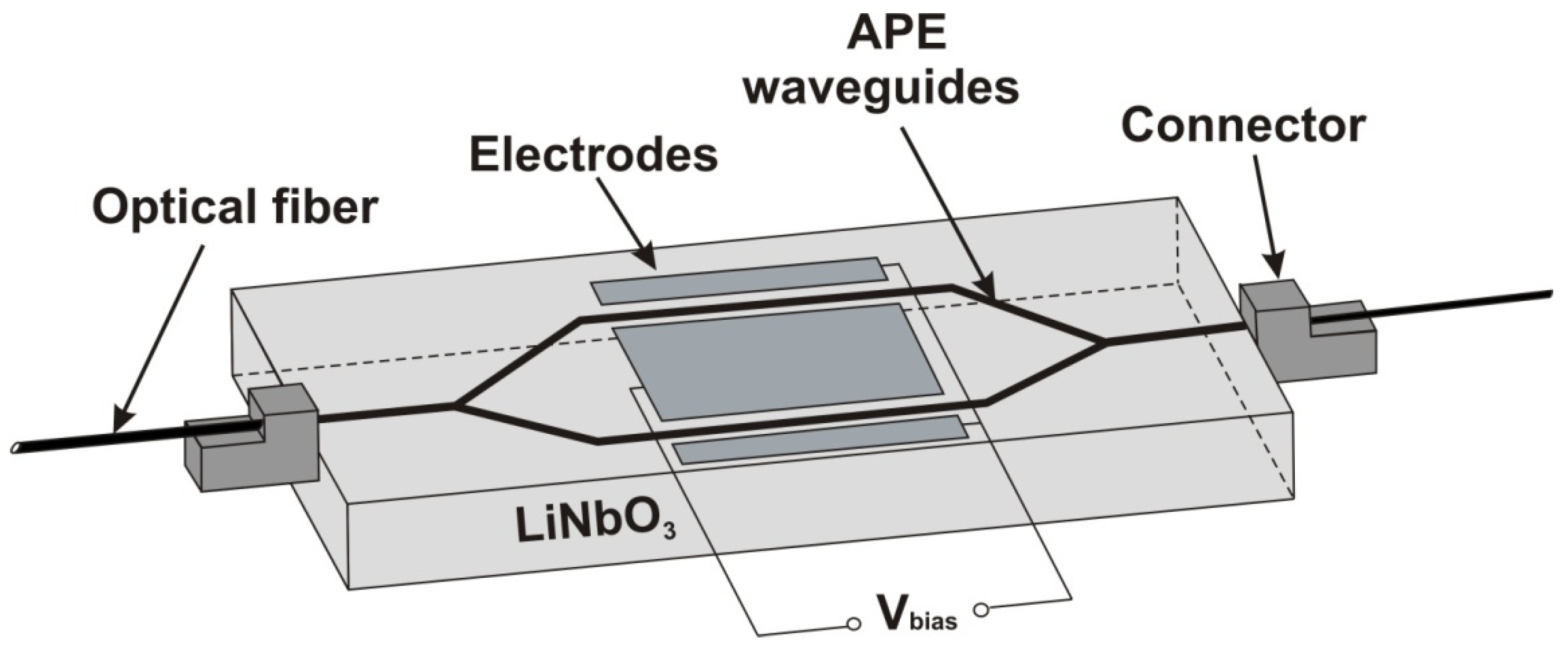
2.1. Sample Preparation

EO-modulators were prepared from congruent LiNbO3 X-cut (manufactured by Crystal Technology Inc., Palo Alto, CA, USA). One of the LiNbO3 wafers was pre-annealed (hereinafter referred to as treatment) at 500 °C for 3 h and then cooled down slowly with a furnace designed for treating the structure of disturbed surface layer as described in [18]. This temperature is ideal for obtaining a more homogeneous structure of the near-surface layer of a LiNbO3 crystal and HxLi1−xNbO3 optical waveguides. Treatment of LiNbO3 directly affects the optical characteristics of APE channel waveguides with identical formation technology. In particular, defects and internal stresses in the near-surface layer of LiNbO3 can increase light scattering passing through optical channel waveguides. Moreover, any defects in the region of the waveguides obtained by ion exchange methods deteriorate the polarizing properties of the waveguide, which results in a decrease in the extinction of the EO-modulator.
APE waveguides were created using direct photolithography. For a protective film, we used an Al2O3 layer (300 nm) deposited by electron beam evaporation. Then, we deposited a positive-acting photoresist (1 μm). After drying and development of the photoresist, its active part was removed in organic solvent. Then, Al2O3 protective film was etched using nitric acid solution and the remains of photoresist were removed. Channels that were 6 μm wide were created.
Proton exchange took place in a closed zirconium reactor at 170 °C for 2 h followed by cooling at 10 °C/min. Annealing was performed at 350 °C for 5.5 h followed by cooling in an oven.
At the next step, we deposited a 0.5 μm layer of gold on a LiNbO3 support surface by vacuum evaporation. In order to make the final structure of electrodes, we also used the process of photolithography and chemical treatment. A couple of samples with optical waveguides and electrodes on their surfaces were cut into 15 mm wide blocks. As a result, we have obtained a couple of chips with treatment LiNbO3 structure and a couple of standard chips that remained unchanged. All chips were obtained at identical process parameters. At the last step, we connected the chips to optical fiber using a NanoMax 311 micromovements system and a machine vision system (Figure 1).
After this, the samples were treated in isopropyl alcohol and de-ionized water for 10 min at each step of producing EO-modulator components.
Speaking of the above processes of creating integral components on the LiNbO3 surface, only proton exchange contributes to changes of the crystal structure rather than related secondary physical and chemical processes:
  • Maximum crystal heating temperature (350 °C) is significantly lower than the temperature when the crystal composition starts to change (above 600 °C), while pyroelectric effect is characteristic of the crystal Z-cut where Li+ ions are redistributed next to two polar faces. These processes are not characteristic of the LiNbO3 X-cut, because the direction of the normal line to the crystal X-cut is nonpolar. Considering strong connections between oxygen base and Nb+5 ions, it is fair to say that the crystal composition does not change in areas where it is not subject to proton exchange when creating waveguides by described methods;
  • Time of photoresist treatment is selected in such a manner that avoids interaction between acid and support structure. As far as the development process is concerned, LiNbO3 is inert to organic developers;
  • UV exposure during connection of the chips and fiber can result in the generation of free electrons in LiNbO3 after photovoltaic effect, but their relaxation time is much less than the time between assembly and testing of the samples.

2.2. Optical Losses

Losses per cm in LiNbO3 crystal were measured on a slope of a back-reflection curve using a Luna OBR-5T-50 reflection meter. The spatial resolution enables taking measurements every 30 μm on a homogeneous linear section within the topology of EO-modulator.
Optical losses were calculated for a wavelength of 1.55 μm by measuring output power of source radiation and after radiation distribution between waveguides of an EO-modulator (fiber-to-fiber). In order to measure optical power, we used the Santec PEM-330 optical power meter.

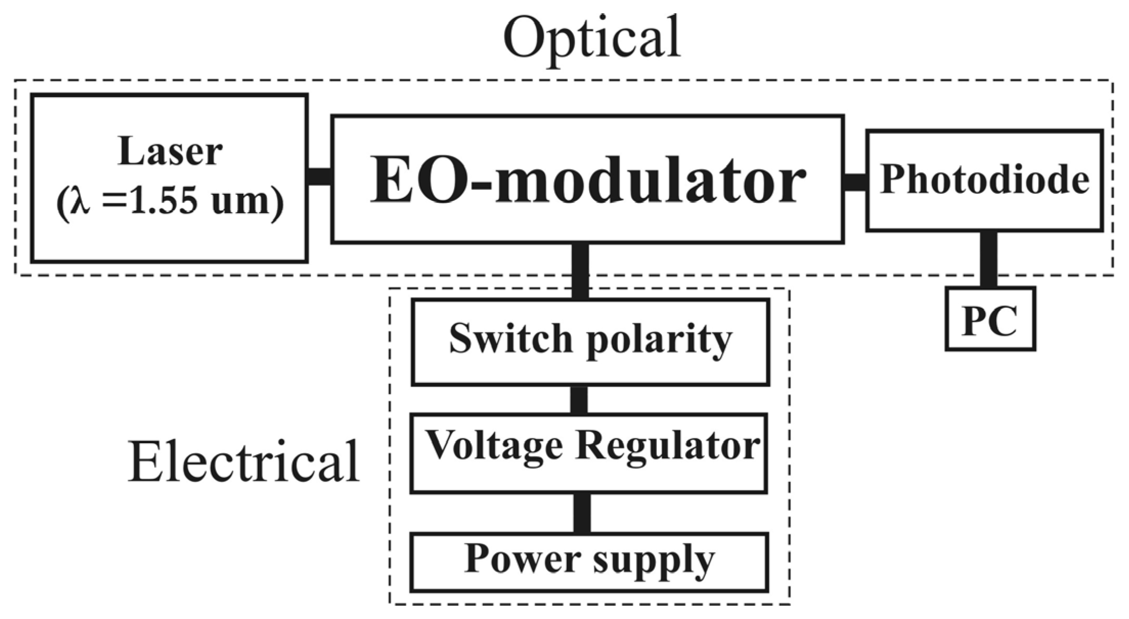
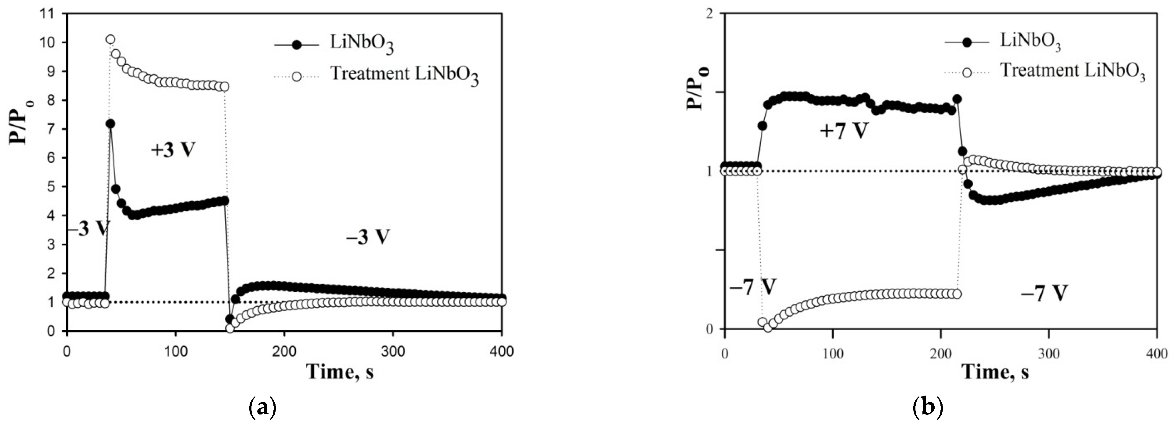
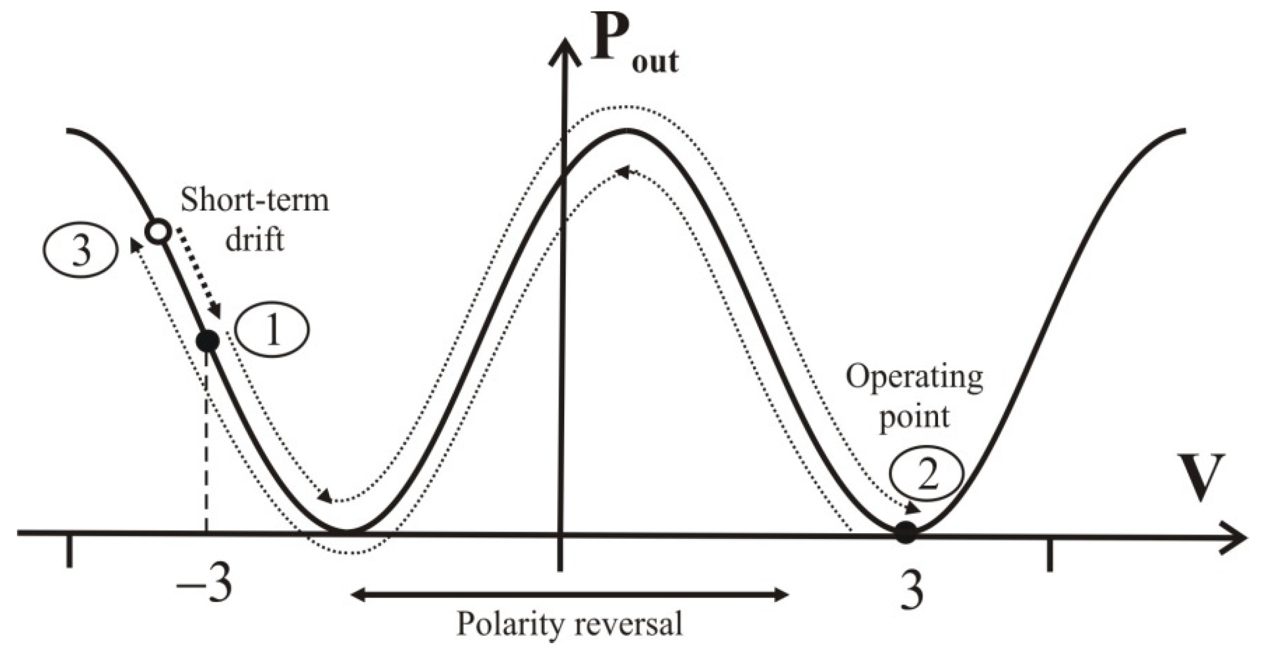
2.3. Drift of Operating Point Depending on Voltage Applied Vbias

We tested short-term drift of an operating point in EO-modulators by applying DC voltage to modulator electrodes and recording changes of the output optical power. Without drift, output optical power should stabilize immediately after voltage is applied to electrodes. However, measurement Pout was changing during a certain period after the voltage was applied. The most interesting results were obtained at hopping changes of the sign of applied voltage. All experiments were performed in the voltage range of ±8 V at an increment of 1 V and holding time of 5 min after the sign of applied voltage changes. We used a battery such as a low noise chemical voltage source. The voltage using a continuously adjusting resistor was manually changed. After that, the polarity at a fixed voltage was changed to study short-term drift. Based on obtained results, we analyzed the relaxation time of operating point of EO-modulators and recovered the transfer function. The lighting source was a highly stable narrow-band laser with a wavelength of 1.55 μm and power of 3 mW. For a layout of the experiment device, refer to Figure 2.

2.4. Drift of Operating Point Depending on Temperature

Temperature measurements were performed to calculate activation energy of DC-drift of operating point of EO-modulators. Understanding activation processes in LiNbO3 near-surface layer in the area of APE channel waveguides and electrodes at temperature effect enabled us to evaluate the effectiveness of LiNbO3 structure treatment and its impact on drift of operating point in EO-modulators. First, we fixed the operating point at a constant voltage of 4.5 V, which corresponds to a linear section of the transfer function for all test samples for a wavelength λ = 1.55 μm. Then, test samples were placed in a heater and heated to 25, 50, 70 and 90 °C with holding time of 7 h (temperature range did not exceed 100 °C according to the manufacturer’s recommendation). Prior to changing the temperature, the samples had to cool down for 12 h. After this, we measured the change of output optical power corresponding to the drift of operating point of EO-modulators.

3. Results and Discussion

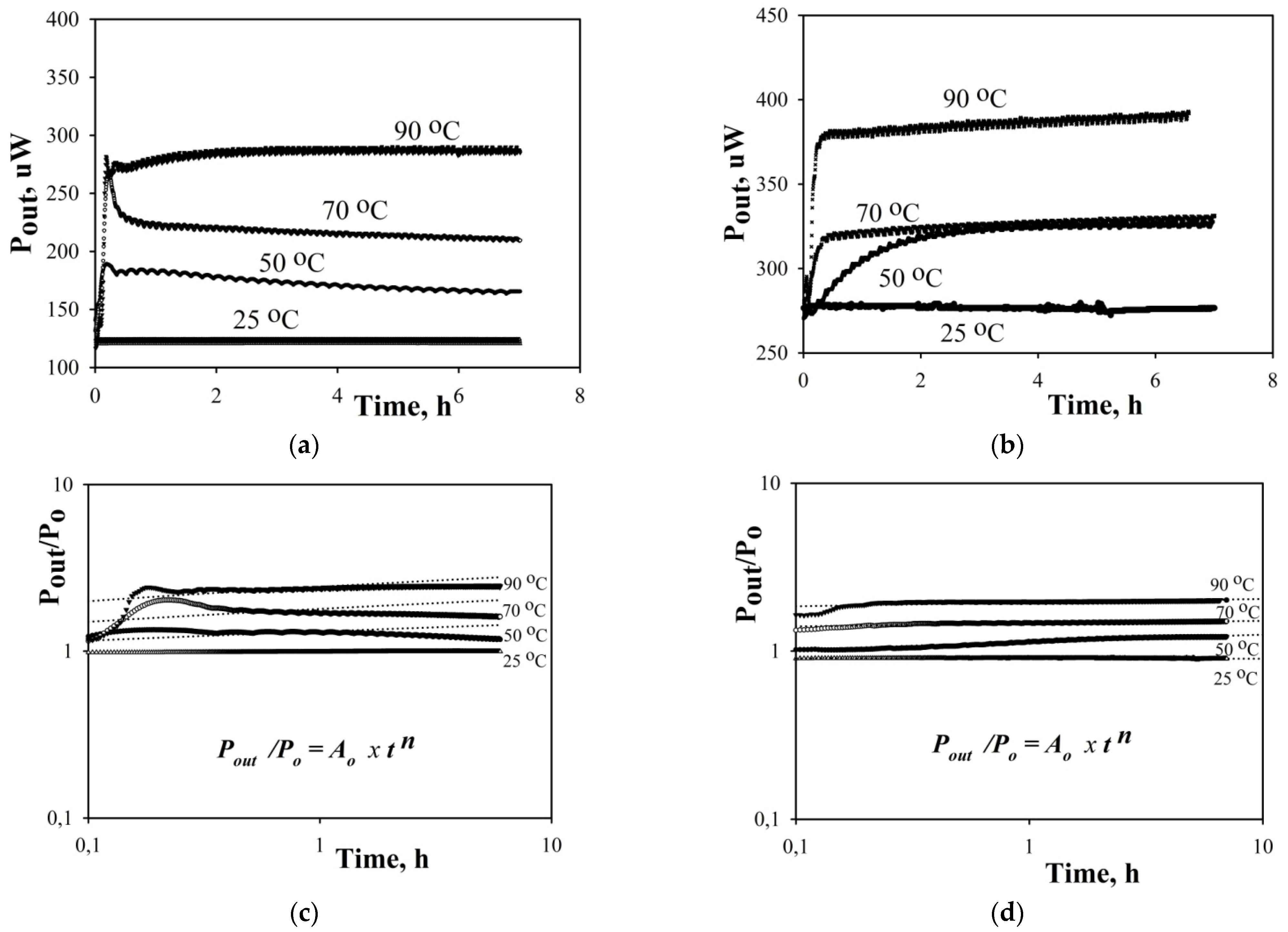
3.1. Short-Term DC-Drift

Prior to testing the stability of DC-drift based on treatment near-surface layer of LiNbO3 crystal in EO-modulators, we measured optical losses both in a chip by an optical reflectometry and in the entire modulator by a fiber-to fiber method. Table 1 shows measured optical losses of the test samples. It is known that optical losses per unit length of stable APE waveguides in a LiNbO3 crystal are ~0.15 dB/cm [19]. The tests resulted in stable APE waveguides with standard characteristics. The spread of loss values per unit length in chips is determined by measurement errors, while the highest optical losses in modulators occur at the connection point of a chip and optical fiber.
Now, observe the impact of applied voltage on changes of Pout based on the structure of near-surface layer of a LiNbO3 crystal. For the measurements of output optical power for applied voltage of 3 and 7 V, refer to Figure 3. Similar results are obtained across the measurement range of ±8 V. When the voltage changes its polarity, the voltage changes its sign to the opposite one and remains unchanged until it is switched back. Therefore, Pout is determined only by processes occurring at a waveguide at every moment, except for the moment of polarity changing.
When polarity changes, output optical power corresponding to the operating point position on the transfer function of EO-modulator changes abruptly (Figure 4). However, the operating point moves to a position that does not correspond to the switching voltage. Accordingly, some relaxation time of the operating point is necessary in order to return to the required position. Figure 4 shows a double voltage switching circuit. After the first switching voltage (position 2, operating point was fixed during 5 min), the second switch of the voltage and the operating point should return to the initial position −3 V. However, the operating point jumped to position 3, which does not correspond to −3 V. There is a certain pattern where the operating point almost always proceeds further than necessary and then returns to initial position 1, which is clearly visible in Figure 3.
Relaxation time of the output optical power to its initial value (variance is less than 1 percent) after double (− → + → −) switching, in our case, is a characteristic of a modulator showing how fast DC-drift becomes extinct. Extinction of DC-drift in EO-modulators after treatment LiNbO3 is two times faster than extinction in reference samples: 116 ± 22 s for annealed wafer samples and 286 ± 37 s for reference samples. This significant difference in relaxation time of DC-drift is determined by a homogeneous structure obtained after treatment of disturbed near-surface layer of LiNbO3 crystal. The treatment process eliminates internal strain (reduces microstrains), removes point defects and dislocations and improves the microstructure, as shown in [16]. After treatment, once voltage Vbias is applied, it is much more difficult for charged defects to move, creating local electric fields in the area of APE waveguides, contributing to changes of refraction index and DC-drift. Thus, our test shows that the structure of the near-surface layer of a LiNbO3 crystal affects drift parameters of EO-modulators through an electro-optical effect and that the method of the layer treatment is effective for increasing the stability of short-term DC-drift.
It is also important to note that the operating point of EO-modulators without treatment structure of the near-surface layer of LiNbO3 crystal is unstable after applied voltage Vbias changes its sign for the first period. This short-term drift in the first period stabilizes very quickly, since these are short-term drift processes associated with a change in the vector of the electric field strength and the movement of charged defects, which will reach an equilibrium depending on the homogeneity of the structure around the waveguides. This is confirmed by long-term studies at room temperature (next section), when the optical power is practically unchanged. The activation energy of internal drift in EO-modulators is analyzed below.
We would like to note that our technique for studying the short-term drift of the operating point is important precisely from a scientific point of view for the detection these rapid changes in EO-modulators.

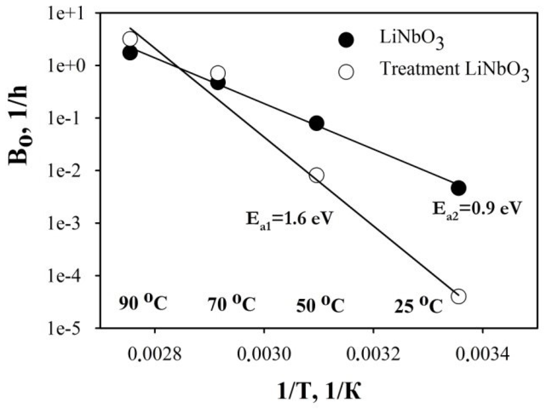
3.2. Temperature Stability of EO-Modulators (Long-Term DC-Drift)

In terms of device operation stability and reliability, it is necessary to know the value of activation energy Ea of DC-drift in EO-modulator. In our research, this parameter is a key to the analysis of temperature impact on DC-drift. Previously, this analysis was performed in [6,20] to evaluate the life cycle of EO-modulators based on LiNbO3 X-cut. The experiment was performed at the following conditions. The operating point was fixed on a linear section of the transfer function at constant voltage V0 = 4.5 V. The experiment showed that as the temperature changes, the operating point drifts and after some time it achieves a new stable state (saturation). Pout can be represented by the following power function:
P o u t ( t ) / P 0 = A 0 · t n
where A0—coefficient; and P0output optical power at V0. The speed of DC-drift decreases as operating time of a device increases d P o u t ( t ) d t ~ t n 1 ; therefore, index n should be within the range of 0 < n < 1. At the same time, output optical power depends on temperature:
P o u t ( t ,   T ) / P 0 = ( B 0 ( T ) · t ) n
where T—temperature; and B 0 ( T ) ~ e E a k T —speed constant proportional to Arrhenius function. Equation (3) shows experimentally observed change of output optical power rather than the full physical nature of DC-drift. This profile can be used for comparative analysis of activation energy of DC-drift in EO-modulators with treatment structure of LiNbO3 near-surface layer. Figure 5 shows Pout dependency on time at various temperatures.
These curves show the change in the position of the operating point on the transfer function of the modulators (Figure 5a,b) with a change in temperature (drift). The operating point moved to a new equilibrium position (tends toward it). The profiles of the experimental curves (Figure 5a,b) are in good agreement with Nagata results [20,21]. Long-term drift consists in a constant slow change Pout around a new equilibrium position. It is important to note that these are exactly slow processes, because the system tends to equilibrium, but the movement of charged defects around the APE-waveguides results in a drift. Thus, for example, in Figure 5b at 50 and 70 °C, Pout almost converges, i.e., the equilibrium points turned out to be close to each other, but at the same time, the activation of the process occurs in different ways.
In order to determine Ea, first we normalized test data according to Equation (3) and then adjusted curves with the simplest (linear) equation relative to the obtained results (Figure 5) to calculate coefficients A0 and n. Using Equations (3) and (4), we calculated the speed constant B0. In order to build the Arrhenius function (Figure 6), we used coefficient data (Table 2) at temperatures of 25–90 °C. From a slope of the plots, Ea was obtained. The activation energies of DC-drift for test samples after treatment and reference samples were 1.6 and 0.9 eV, respectively. The obtained values are not the direct activation energy of the material, but they relate to the entire test system according to Equation (3). However, what is more important for us is the comparative analysis of DC-drift in EO-modulators after treatment with LiNbO3 structure obtained at identical process conditions and Ea calculations. The activation energy for treatment LiNbO3 is about two times higher. In order to switch the entire system to an unstable state, one should use two times more energy. In other words, system stability increases after treatment of LiNbO3 structure and DC-drift decreases.
This results from the reduction in charged defects in the area of APE channel waveguides and LiNbO3 near-surface layer are described as the main source of DC-drift in EO-modulators in the previous section and in [15].
In paper [6], the obtained values of activation energy of DC-drift (0.7, 1.0 and 1.2 eV) were used to evaluate the number of failures occurring during operation of EO-modulators over 20 years. The number of failures at 50 °C was three errors with Ea = 1.2 eV, 25 errors with Ea = 1.0 eV and 260 errors with Ea = 0.7 eV. Therefore, the higher the activation energy of DC-drift, the better the stability of the entire device, resulting in a smaller number of errors during long-time operation of EO-modulators. The obtained comparative results were Ea1/Ea2 = 1.8, where Ea1 is the activation energy of a modulator after treatment LiNbO3 and Ea2 is the activation energy of a references modulator that enables us to draw a firm conclusion that LiNbO3-based EO-modulators can operate longer with a smaller number of errors at the defined driver parameters after treatment near-surface structure.
Reported Ea varies between 1.0 eV and 1.4 eV for unbuffered X-cut LiNbO3 [21,22]. This range of activation energies means a broad range of acceleration factors. Our result with Ea = 1.6 eV agrees quite accurately with these data and demonstrates the reliable long-term behavior of EO-modulators after treatment.
Thus, temperature tests showed significant improvement in drift parameters of EO-modulators after treatment with LiNbO3 structure. Our idea of improving the operation stability of EO-modulators by monitoring material parameters of the transfer function has proved its effectiveness at various experimental conditions and can be applied to systems based on other optical materials.

4. Conclusions

This study was focused on testing the impact of material parameters of the transfer function (defective microstructure of near-surface layer of a LiNbO3 crystal) on the stability of EO-modulator characteristics. We performed comprehensive analysis of the effect of LiNbO3 microstructure treatment on the level of DC-drift in EO-modulators, enabling us to draw the following conclusions:
  • Relaxation time of short-term drift of operating point decreases from 286 to 116 s;
  • Activation energy of operating point in EO-modulators showed growth from 0.9 to 1.6 eV.
Thus, EO-modulators demonstrated a more stable state of the system in general. All results obtained in this study support each other, demonstrating the impact of material factors of the transfer function on DC-drift in EO-modulators. Our treatment method for the structure of the disturbed near-surface layer of a LiNbO3 crystal proved its effectiveness in reducing short and long-term drifts in EO-modulators.

Author Contributions

Conceptualization and drift experiments, A.S.; methodology and writing, R.P.; formal analysis and optic measurements, A.Z.; resources and creation samples, S.M. and M.K. All authors have read and agreed to the published version of the manuscript.

Funding

This research was funded by RFBR and Perm Territory, project number 20-42-596001 (samples study), and Ministry of Education and Science of Perm region under Contract No. C-26/848 (samples design).

Institutional Review Board Statement

Not applicable.

Informed Consent Statement

Not applicable.

Data Availability Statement

Data underlying the results presented in this paper are not publicly available at this time but may be obtained from the authors upon reasonable request.

Conflicts of Interest

The authors declare no conflict of interest.

References

  1. Noguchi, K. Lithium Niobate Modulators. In Broadband Optical Modulators: Science, Technology, and Applications; Chen, A., Murphy, E.J., Eds.; CRC Press: Boca Raton, FL, USA, 2012; pp. 151–172. [Google Scholar]
  2. Rao, A.; Fathpour, S. Compact Lithium Niobate Electrooptic Modulators. IEEE J. Sel. Top. Quantum Electron. 2018, 24, 1–14. [Google Scholar] [CrossRef]
  3. Han, H.; Xiang, B. Integrated electro-optic modulators in x-cut lithium niobate thin film. Optik 2020, 212, 164691. [Google Scholar] [CrossRef]
  4. Wooten, E.L.; Kissa, K.M.; Yi-Yan, A.; Murphy, E.J.; Lafaw, D.A.; Hallemeier, P.F.; Maack, D.; Attanasio, D.V.; Fritz, D.J.; McBrien, G.J.; et al. Review of lithium niobate modulators for fiber-optic communications systems. IEEE J. Sel. Top. Quantum Electron. 2000, 6, 69–82. [Google Scholar] [CrossRef]
  5. Nagata, H. Long-term DC drift in x-cut LiNbO3 modulators without oxide buffer layer. IEE Proc.-Optoelectron. 2000, 147, 350–354. [Google Scholar] [CrossRef]
  6. Nagata, H.; Papasavvas, N. Bias stability of OC48 x-cut lithium-niobate optical modulators: Four years of biased aging test results. IEEE Technol. Lett. 2003, 15, 42–44. [Google Scholar] [CrossRef]
  7. Hofer, L.R.; Schaeffer, D.B.; Constantin, C.G.; Niemann, C. Bias Voltage Control in Pulsed Applications for Mach-Zehnder Electrooptic Intensity Modulators. IEEE Trans. Control Syst. Technol. 2017, 25, 1890–1895. [Google Scholar] [CrossRef]
  8. Yuan, X.; Zhang, J.; Zhang, M. Any point bias control technique for MZ modulator. Optik 2019, 178, 918–922. [Google Scholar] [CrossRef]
  9. Svarny, J. Analysis of quadrature bias-point drift of Mach-Zehnder electro-optic modulator. In Proceedings of the 2010 12th Biennial Baltic Electronics Conference, Tallinn, Estonia, 4–6 October 2010; pp. 231–234. [Google Scholar]
  10. Cho, P.S.; Khurgin, J.B.; Shpantzer, I. Closed-Loop Bias Control of Optical Quadrature Modulator. IEEE Photonic Technol. Lett. 2006, 18, 2209–2211. [Google Scholar] [CrossRef]
  11. Wang, L.L.; Kowalcyzk, T.A. Versatile Bias Control Technique for Any-Point Locking in Lithium Niobate Mach-Zehnder Modulators. J. Lightwave Tech. 2010, 28, 1703–1706. [Google Scholar] [CrossRef]
  12. Toney, J.E.; Stenger, V.E.; Pollick, A.; Sriram, S. Operating Point Correction for Mach Zehnder Interferometer-based Electro-optic E-field Sensors. In Proceedings of the Optical Sensors and Sensing Congress (ES, FTS, HISE, Sensors), San Jose, CA, USA,, 25–27 June 2019; p. SW4C.1. [Google Scholar]
  13. Bui, D.T.; Nguyen, C.T.; Ledoux-Rak, I.; Zyss, J.; Journet, B. Instrumentation system for determination and compensation of electro-optic modulator transfer function drift. Meas. Sci. Technol. 2011, 22, 125105. [Google Scholar] [CrossRef]
  14. Fu, Y.; Zhang, X.; Hraimel, B.; Liu, T.; Shen, D. Mach-Zehnder: A Review of Bias Control Techniques for Mach-Zehnder Modulators in Photonic Analog Links. IEEE Microw. Mag. 2013, 14, 102–107. [Google Scholar] [CrossRef]
  15. Salvestrini, J.P.; Guilbert, L.; Fontana, M.; Abarkan, M.; Gille, S. Analysis and Control of the DC Drift in LiNbO3-Based Mach-Zehnder Modulators. J. Lightwave Technol. 2011, 29, 1522–1534. [Google Scholar] [CrossRef]
  16. Sosunov, A.V.; Ponomarev, R.S.; Yuriev, V.A.; Volyntsev, A.B. Effect of the structure and mechanical properties of the near-surface layer of lithium niobate single crystals on the manufacture of integrated optic circuits. Optoelectron. Instrum. Data Process. 2017, 53, 82–87. [Google Scholar] [CrossRef]
  17. Piecha, J.; Molak, A.; Breuer, U.; Balski, M.; Szot, K. Features of surface layer of LiNbO3 as-received single crystals: Studied in situ on treatment samples modified by elevated temperature. Solid State Ion. 2016, 290, 31–39. [Google Scholar] [CrossRef]
  18. Sosunov, A.; Ponomarev, R.; Semenova, O.; Petukhov, I.; Volyntsev, A. Effect of pre-annealing of lithium niobate on the structure and optical characteristics of proton-exchanged waveguides. Opt. Mater. 2019, 88, 176–180. [Google Scholar] [CrossRef]
  19. Suchoski, P.G.; Findakly, T.K.; Leonberger, F.J. Stable low-loss proton-exchanged LiNbO3 waveguide devices with no electro-optic degradation. Opt. Lett. 1988, 13, 1050–1052. [Google Scholar] [CrossRef] [PubMed]
  20. Nagata, H. Activation Energy of DC-Drift of X-Cut LiNbO3. IEEE Photonic Technol. Lett. 2000, 12, 386–388. [Google Scholar] [CrossRef]
  21. Nagata, H.; Ishizuka, Y.; Akizuki, K. Temperature dependency of X-cut LiNbO3 modulator dc drift. Electron. Lett. 2000, 36, 1952–1953. [Google Scholar] [CrossRef]
  22. Nagata, H.; Li, Y.; Croston, I.; Maack, D.R.; Appleyard, A. Dc drift activation energy of LiNbO3 optical modulators based on thousands of hours of active accelerated aging tests. IEEE Photon. Technol. Lett. 2002, 14, 1076–1078. [Google Scholar] [CrossRef]
Figure 1. Schematic of EO-modulator.
Photonics 08 00571 g001
Figure 2. Schematic of DC-drift measurements.
Photonics 08 00571 g002
Figure 3. Short-term DC-drift at ±3 (a) and ±7 V (b).
Photonics 08 00571 g003
Figure 4. Mechanism of short-term DC-drift measurements.
Photonics 08 00571 g004
Figure 5. DC-drift curves measured on EO-modulators at 50, 70 and 90 °C: reference (a,c) and after treatment LiNbO3 (b,d). Plots (c,d) are replots of (a,b).
Photonics 08 00571 g005
Figure 6. Arrhenius plots of experimental EO-modulators.
Photonics 08 00571 g006
Table 1. Optical losses and half-wave voltage.
CharacteristicAPE
Waveguide loss, dB/cm0.13–0.17
Average fiber-to-fiber loss, dB6.5
Half-wave voltage, V3.5–6
Table 2. Calculated parameters on DC-drift of EO-modulators.
SampleTemperature, °CCoefficient, A0Coefficient, nCoefficient, B0 [1/h]
LiNbO3250.9840.0030.0046
500.8420.0680.079
700.9090.1280
901.1120.1911.745
Treatment LiNbO3250.9810.0020.00004
500.7830.0510
700.9920.0241
901.050.0433
Publisher’s Note: MDPI stays neutral with regard to jurisdictional claims in published maps and institutional affiliations.

