1. Introduction
Currently, research in the field of developing devices that use photons as the main carrier of information is gaining more and more relevance. A special place has been occupied by research related to the use of optical waveguides and resonators using whispering-gallery-mode (WGM) designs. The reason is that such waveguide structures have a high Q-factor and relatively low optical losses in combination with a small volume of the mode [
1].
It is possible to build optical filters using WGM resonators [
2], narrow-band lasers with external resonant feedback [
3,
4], tunable delay lines [
5,
6] used for buffering signals, optical or radio frequency (RF) phase arrays [
7], sensors [
8,
9], the creation of micro-opto-electromechanical gyroscopic systems [
10] and other applications in the field of integrated photonics [
11]. The possibility of generating coherent frequency combs and forming solitons in optical microresonators [
12,
13] has the potential to create compact spectrometers [
14,
15], low-noise RF sources [
16], as well as optical frequency synthesizers [
17].
For all these applications, the high Q-factors of resonators in devices are crucial. The use of high-Q resonators allows reducing the threshold for generating a parametric comb, increasing time delays and the sensitivity of a refractive index during sensing and improving frequency discrimination.
The research and wide application of WGM waveguides and resonators directly depends on how accessible and reproducible their manufacturing technology will be. Typical ultra-high-quality (UHQ) resonators made in the form of microspheres and microtoroids, due to their design and technological features, cannot be integrated into photonic integrated circuits (PICs) [
10]. In this regard, alternatives that are compatible with silicon technology were proposed.
Silicon is one of the most promising materials for generating Kerr frequency combs [
13] in the near- and mid-infrared frequency range due to the high Kerr nonlinearity. However, the use of silicon microresonators is limited due to relatively low Q-factors in some spectral ranges [
18].
In this article, we present a silicon disk resonator manufactured by silicon technology using group-processing methods, the calculated Q-factor of which is 107. In addition, we give a detailed description of the technique for studying the surface roughness of a silicon resonator with a nonlinear profile.
2. Fabrication
One of the main criteria in the development of a method for creating an ultrahigh-Q silicon disk resonator is the need for its implementation using silicon technologies and group-processing methods. The choice of design parameters, such as the value of the “undercut”, ‘’legs’’ and the angle of the wedge-shaped profile, was based on previous studies [
19,
20].
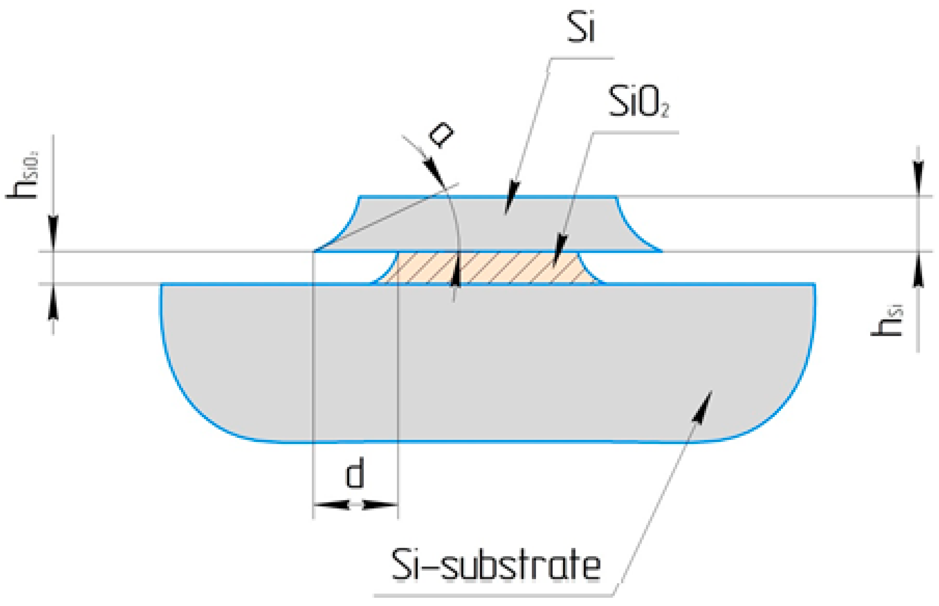
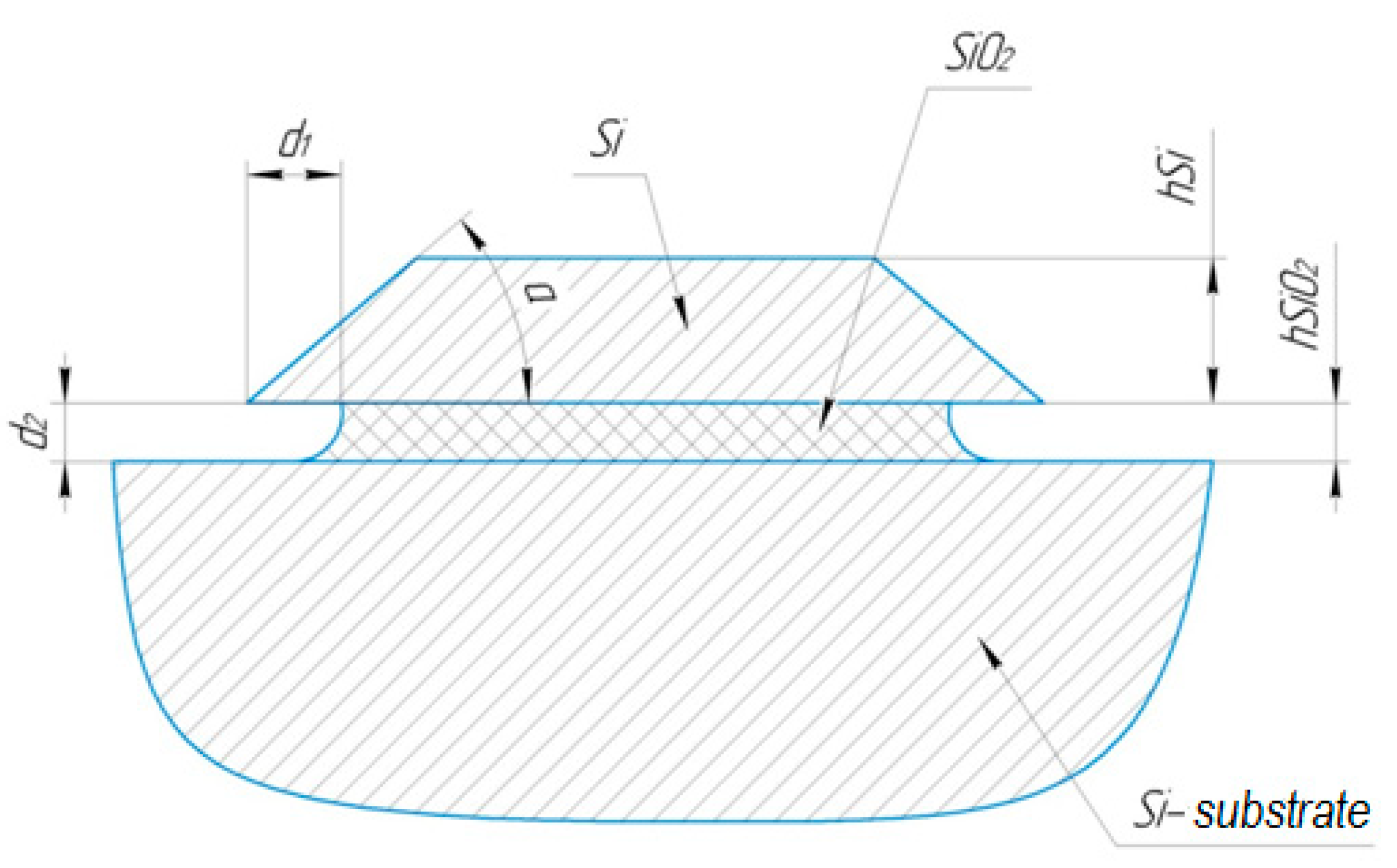
Figure 1 shows the schematic of the profile of the developed structure.
The topology of the resonators is formed by standard photolithography methods, followed by a set of standard technological processes used for the formation of integrated circuits and MEMS.
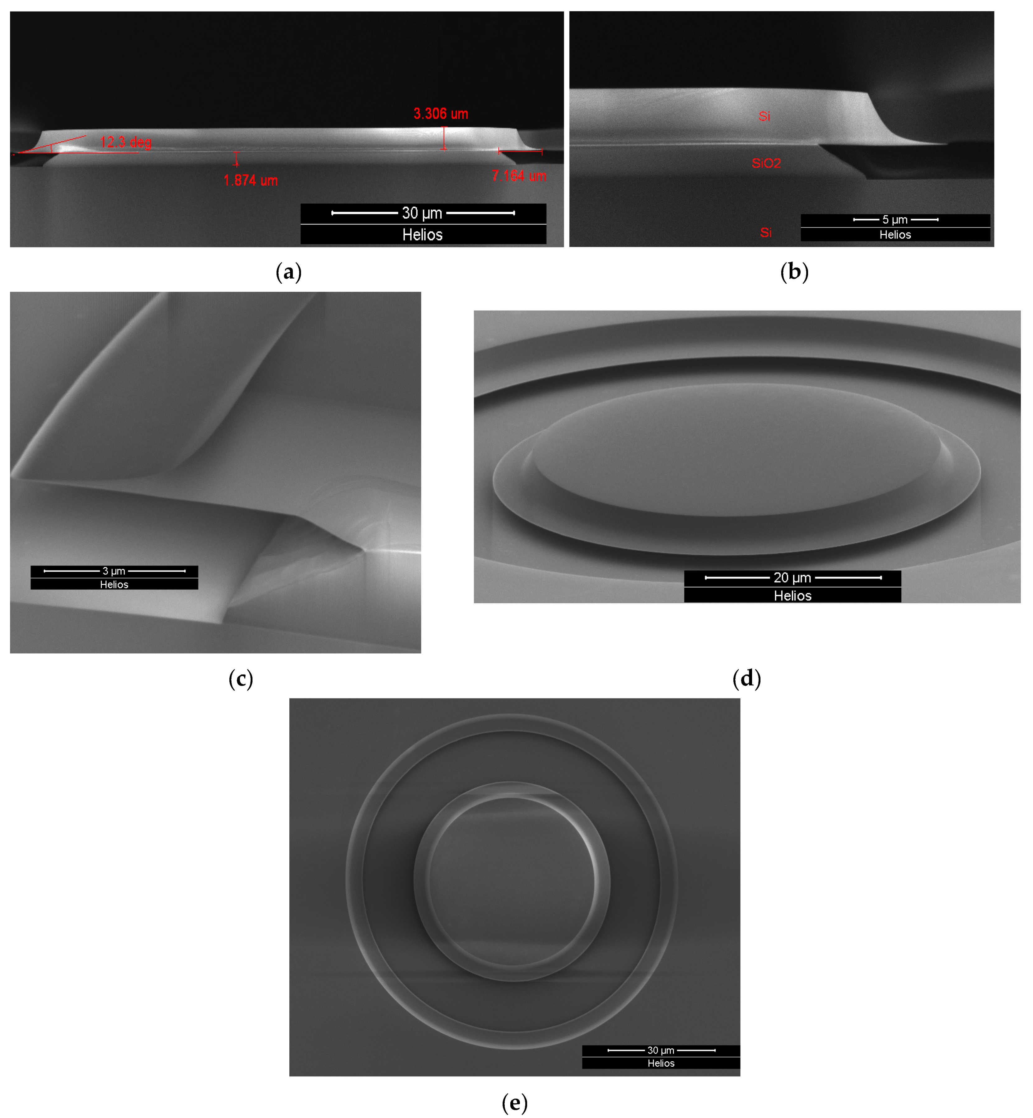
Figure 2 shows the SEM images of silicon disk WGM resonators with a wedge-shaped profile. In the SEM images presented, the surface of the resulting structure had minimal roughness. The estimation of the numerical value of the roughness is described in
Section 3 of this article.
The structures surrounding the WGM resonator were buffer technology areas. The value of the wedge-shaped profile angle was 12.3°, which is of particular interest for further studies of such a resonator. Using previously proven technology approaches, it was difficult to achieve such a profile in silicon. These experimental results demonstrated the possibility of adjusting the angle and obtaining the lower surface roughness of the silicon resonator.
3. Evaluation of the Surface Roughness of Silicon Resonators
In order to establish the influence of the surface roughness of the resonator on the value of its Q-factor, a quantitative assessment of the surface roughness of the manufactured samples was performed using a Helios 650 scanning electron microscope. The research of Japanese authors [
21,
22], as well as previously presented developments [
23], was taken as the basis for the development of the technique. The purpose of the method is to study the horizontal edge of an etched element.
3.1. Roughness Analysis Using a Helios 650 Scanning Electron Microscope
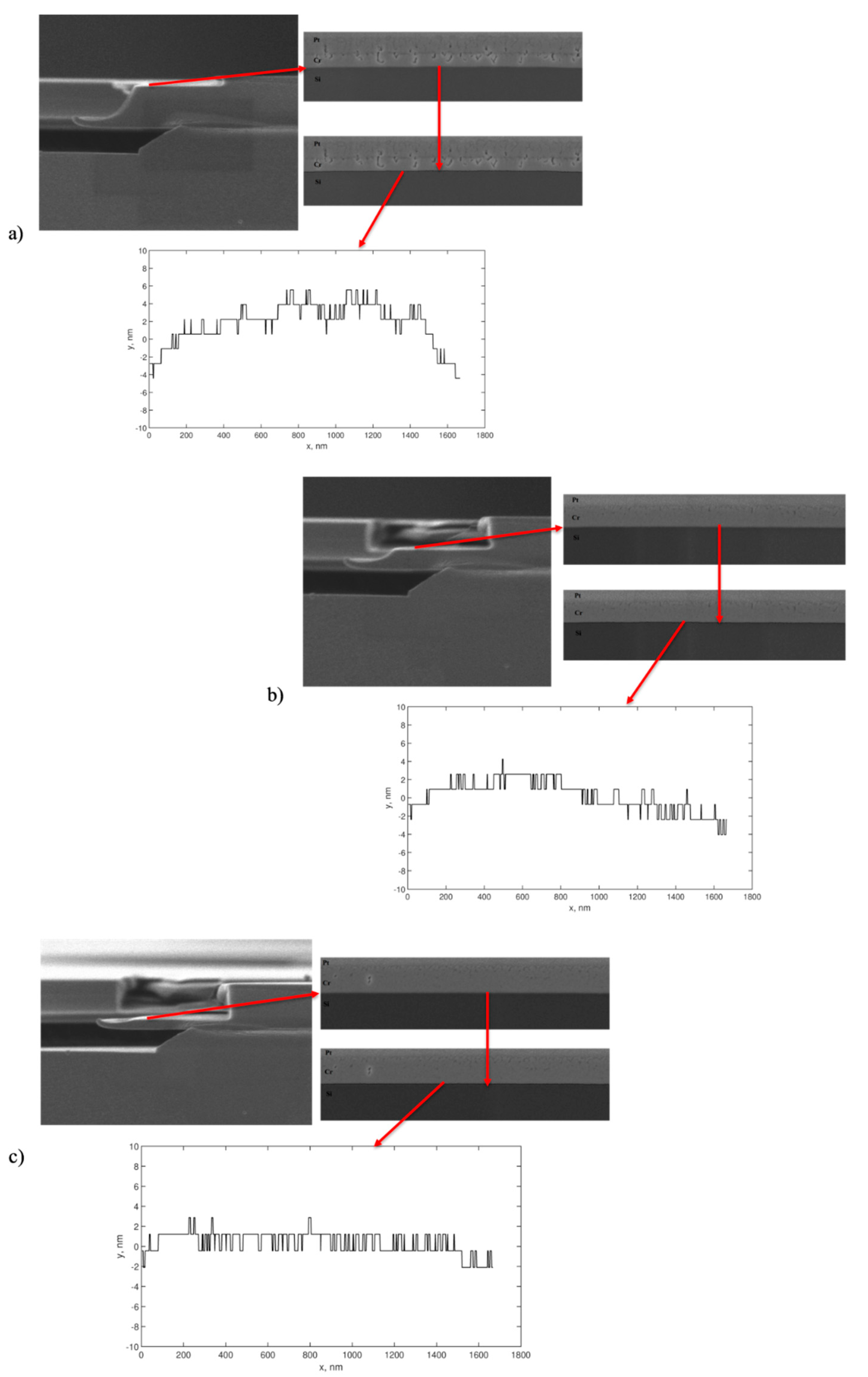
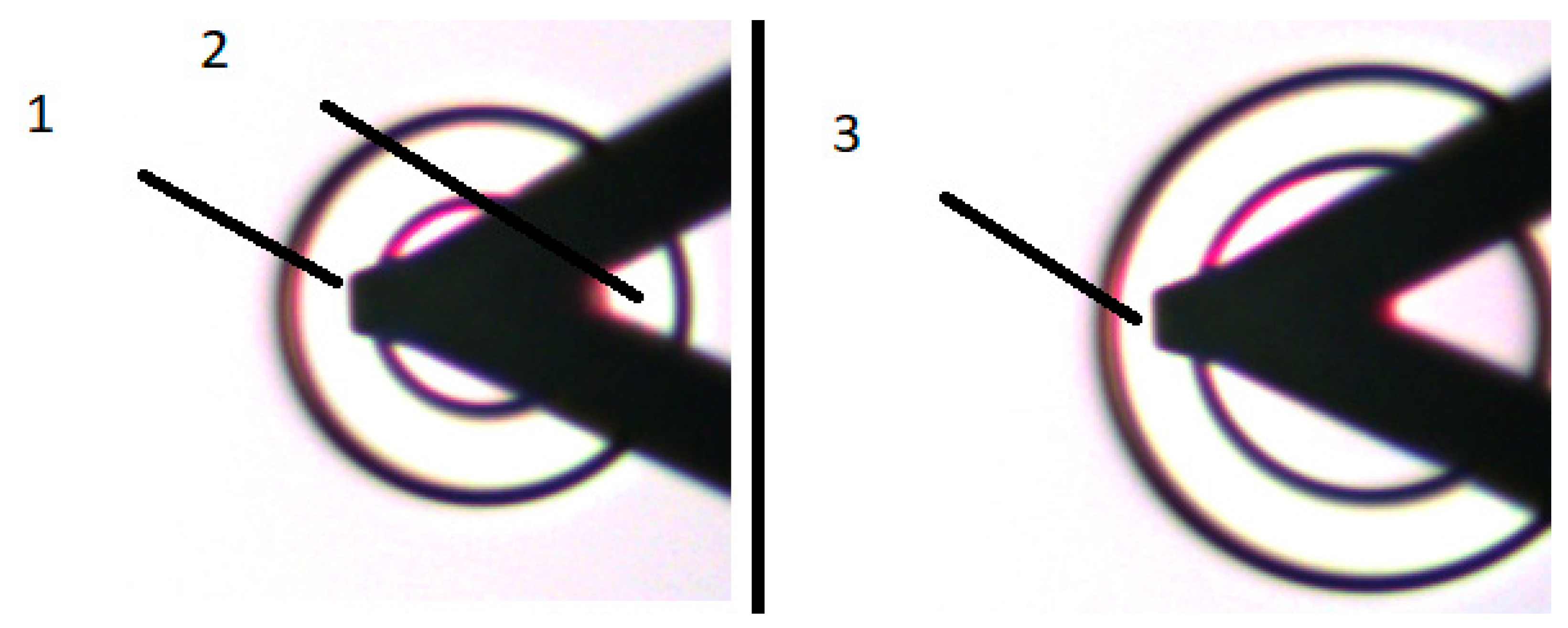
Cr and Pt layers were formed on the selected area of the studied structure, and then the area of study was removed using an ion beam (
Figure 3).
Three regions of the resonator diameter were selected for the study. In each area, 3 cuts were made using an ion beam, i.e., closer to the upper edge of the profile (
Figure 4a), at the bend point of the profile (
Figure 4b), and near the wedge (
Figure 4c). A picture at a 250,000 magnification was taken in each region, showing the interface between the silicon structure and the metal. Then, the analysis of the obtained image was carried out by selecting the element border at the maximum gradient, followed by constructing the border profile (
Figure 4). The length of the structure section in the image was 1.5 µm.
Since the profile of the studied area had a bend, we used the average value of the spread over the straight region, which was about 2 nm, to quantify the roughness.
3.2. Roughness Analysis Using Bruker AFM
At the same time, we used a Bruker atomic force microscope AFM to determine the roughness of the silicon disk resonator profile, as well as to test the method described in
Section 3.1. The samples were scanned using a ScanAsyst Air probe with a V-shaped cantilever, with a nominal radius of the probe tip curvature of 2 nm.
Scanning was made in three areas (
Figure 5), each of which was divided into several sub-areas.
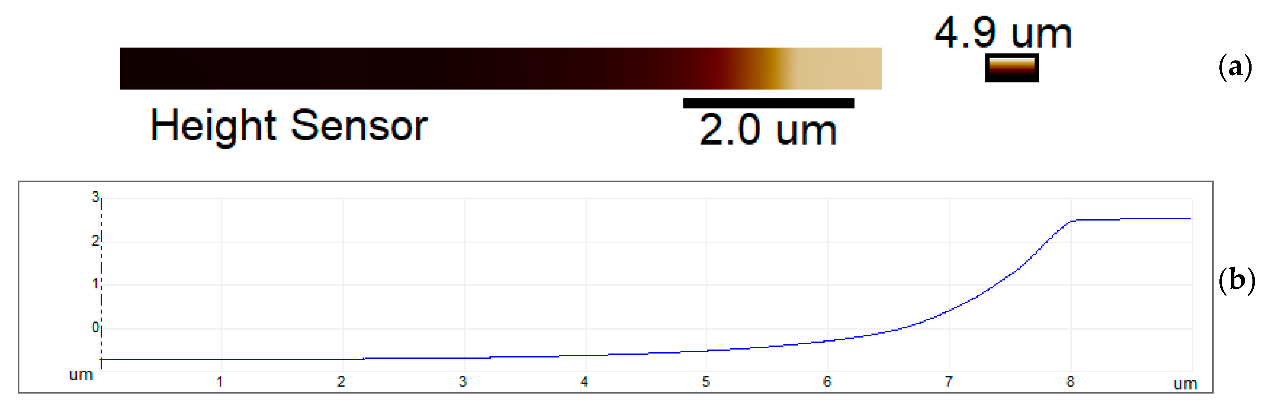
Figure 6 shows the AFM scan and its cross-section along the entire length of the ascent in area 1 in
Figure 5.
For a more accurate analysis of the roughness in area 1, three sub-areas with a length of 1 μm were determined (S1, at the beginning; S2, in the middle; S3, at the end of the rise). Thus, the lateral resolution was approximately 1 nm.
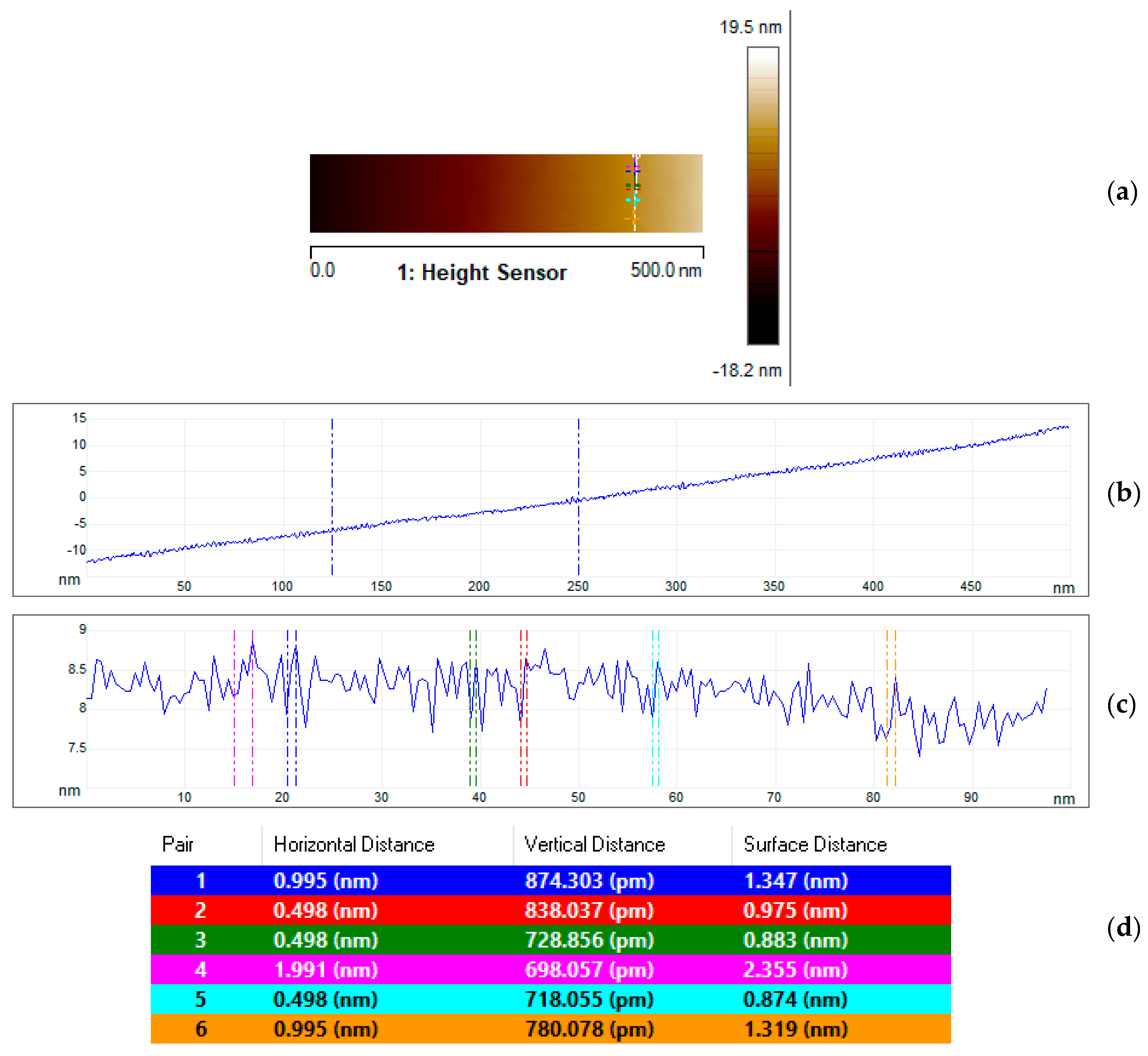
Figure 7 shows an AFM scan of sub-area S1 (its horizontal and vertical sections). The roughness of the sample was determined in terms of a vertical section (perpendicular to the scanning direction). The table (
Figure 7a) shows the values of the horizontal and vertical distances between the markers indicated in
Figure 7c. The colors of the markers correspond to the colors of the rows in the table. This approach maximizes the elimination of the influence of the sample geometry (tilt) on the difference in height between the peaks.
The arithmetic mean of the profile deviation from the baseline Ra was 0.179 nm.
The mean square deviation Rq was 0.225 nm.
Next, according to a similar principle, data were given for sub-areas S2 and S3 of area 1, similar sub-areas S4 and S5 of area 2, and S6 and S7 of area 3. The results are presented in
Table 1.
The measured values of the arithmetic mean deviation of the Ra profile over the entire area did not exceed 1 nm, which is at the limit of the resolution of the technique. At the same time, it is obvious that as the steepness of the studied area increased, the roughness increased slightly. By comparing the surface roughness values of the silicon WGM resonator with two different methods, we can conclude that the results agree well with each other.
3.3. Results of the Surface Roughness of the WGM Resonator, Manufactured Using a Different Technological Approach
Previously, we presented a method for forming a silicon disk resonator with a wedge-shaped profile. The schematic of its cross-section is shown in
Figure 8 [
19].
The method of creating such a resonator was described earlier [
19], and it involves the use of plasma-chemical etching to form the desired profile.
The roughness of such a silicon disk resonator was quantified using the method described in
Section 3.1. It was about 30–40 nm.
4. Calculation of the Q-Factor and the Degree of Localization of the Light Flux in the Studied Silicon Disk Resonators
Based on the data obtained in
Section 3, using the Q-factor calculation equation that takes into account the roughness of its surface [
24,
25], we made a preliminary approximate calculation of the Q-factors of the resonators:
where
n is the refractive index of the host material,
λ is the optical wavelength, and
D is the diameter of the resonator, while
σ and
B are the RMS (root mean square) roughness and its correlation length, respectively.
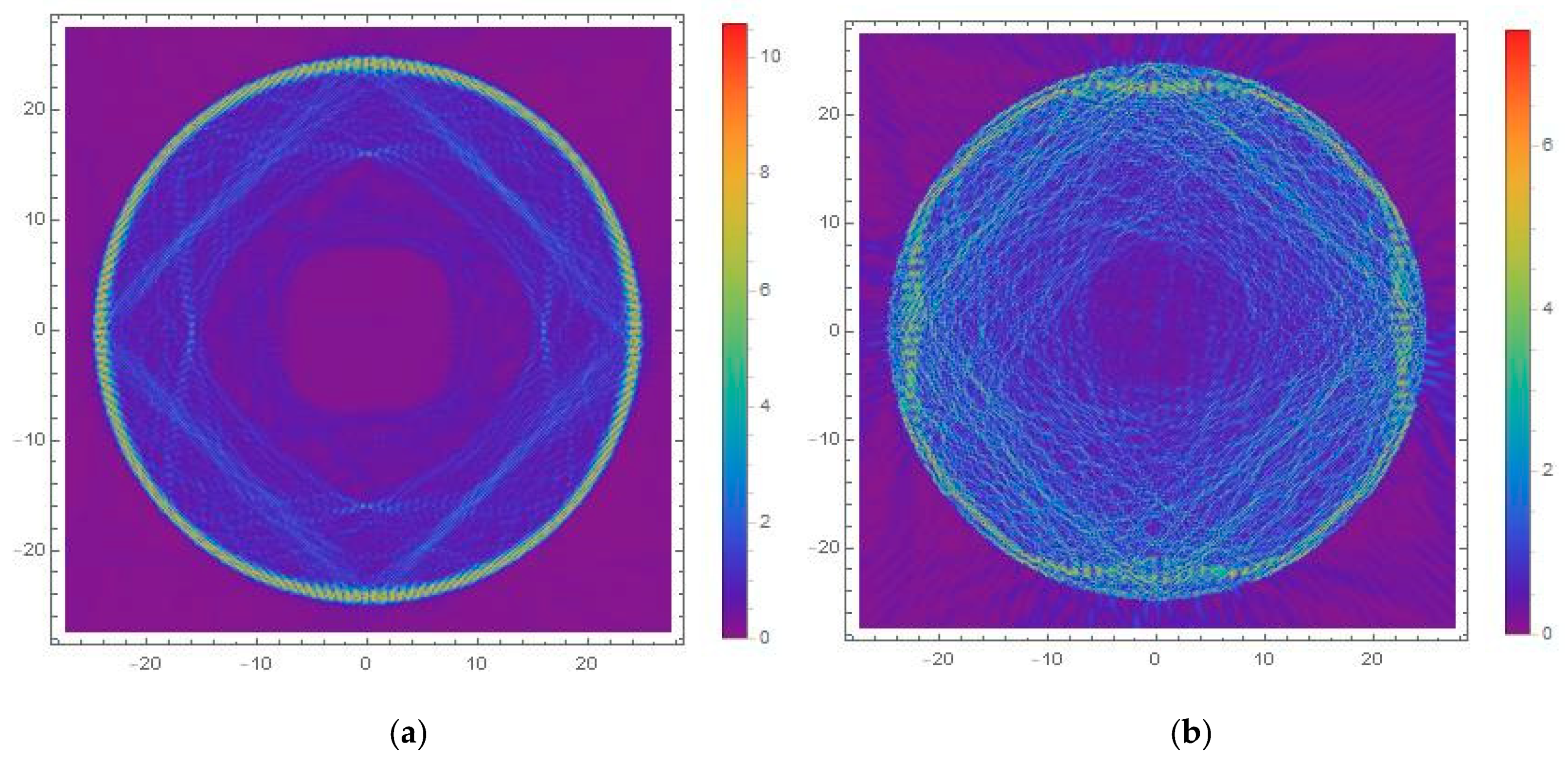
To calculate Q-factors of real rough resonators, we used the finite-difference time-domain (FDTD) method. It assumes that a short pulse is launched into the studied object and the Q-factor is determined by its attenuation. A point dipole polarized in the tangential direction is a source to launch the field into the resonator. The fields of modes calculated in this way are shown in
Figure 9. In
Figure 9, it can be seen that the WGM field was localized near the edge of the disk. The square-shaped field strength closer to the center of the disk was the field from the exciting dipole. Due to the WGM resonance effect, the field of the exciting dipole attenuated stronger than the field of the resonant mode.
It should be noted that the FDTD method uses a short pulse containing a certain frequency spectrum to excite the field in a system. The shorter the pulse, the wider the spectrum, so it is not necessary to select the size of a resonator or the frequency of an input wave to fine-tune the resonance, while in the case of a wide pulse, several resonant frequencies can be excited in the resonator.
At the same time, we calculated the Q-factors of the resonators numerically using the FDTD method.
Figure 9 shows the schematic of the field distribution in the disk resonator at the roughness value
σ of 1 nm (
Figure 9a) and at a roughness value
σ of 40 nm (
Figure 9b). The electric field was excited by four point dipole sources located near the edge of the disk along the straight lines
x = 0 and
y = 0. It can be seen in
Figure 9a that the roughness
σ of 1 nm did not negatively affect the formation of the WGM. The mode was formed near the edge of the disk (some distortions of the mode shape were associated with the presence of point sources), while the roughness
σ of 40 nm led to a significant distortion of the excited mode (
Figure 9b). In addition, as can be seen in
Figure 9b, the field in the case of a large roughness was not completely localized inside the resonator. Therefore, there was a significant energy leakage, leading to a significant decrease in its Q-factor.
The Q-factor of the resonator was estimated from the decay time of a pulse launched into the resonator as following:
where
fR is the resonant frequency,
e is the base of the natural logarithm, and
m is the parameter of pulse attenuation. The time estimates for the modes in
Figure 9 are shown in
Table 2.
The results of the calculations are presented in
Table 2.
The correlation length of the roughness was taken equal to 10σ [
24].
5. Conclusions
The methods for studying the surface roughness of a WGM resonator with a nonlinear profile presented in this work agree with each other. This makes it possible to obtain reliable information on the values of the surface roughness of structures with various non-standard profiles, as well as those of structures made of any materials compatible with silicon technology. Thus, we can say that this method can be used to analyze the influence of various technological approaches to the production of WGM resonators using silicon technology on the amount of surface roughness.
Based on the obtained data, it was found that in the case of a decrease in the surface roughness of the resonator by an order of magnitude (from 30–40 nm to 1–2 nm), its Q-factor increased by three orders of magnitude (from 104 to 107). It allows getting ultrahigh-Q silicon WGM resonators. Based on this fact, we can conclude that the surface roughness of the WGM resonator has a strong influence on its Q-factor. In addition, the technological approach to the production of resonators studied in this work is fully compatible with silicon technology, involves the use of group processing methods, which allows us to significantly expand the scope of their application, and increases prospects for integrating such resonators into PICs. In addition, the use of such resonators allows reducing the cost of each unit of a product, which will significantly increase prospects for their wide distribution and application in PICs.
Author Contributions
Conceptualization, A.V.Y. and V.V.S.; methodology, A.V.Y. and A.S.K.; software, A.S.K.; validation, V.V.A. and S.S.G.; formal analysis, A.V.Y. and A.S.K.; investigation, A.V.Y.; resources, V.V.A. and V.V.S.; data curation, V.V.A., V.V.S., and S.S.G.; writing—original draft preparation, A.V.Y.; writing—review and editing, D.V.G.; visualization, A.V.Y. and D.V.G.; supervision, V.V.A. and S.S.G.; project administration, V.V.A. and V.V.S.; funding acquisition, V.V.A. and S.S.G. All authors have read and agreed to the published version of the manuscript.
Funding
This article was prepared with the financial support from the Ministry of Education and Science of the Russian Federation as part of the State Assignment for 2019 (project No. 0N59-2019-0020) “Theoretical and experimental studies of structural and technological methods for creating integrated optics elements compatible with silicon technology”. The etching process was carried out for using equipment “Functional control and diagnostics of micro- and nanosystem technology” on the basis of SMC “Technological Centre”.
Acknowledgments
This work was supported by theoretical and experimental studies of structural and technological methods for creating integrated optics elements compatible with silicon technology. The etching process was carried out using equipment “Functional control and diagnostics of micro- and nanosystem technology” on the basis of SMC “Technological Centre”.
Conflicts of Interest
The authors declare no conflict of interest.
References
- Gorodetsky, M.L. Optical Microresonators with Giant Quality–Factor; Fizmatlit: Moscow, Russia, 2011. [Google Scholar]
- Monifi, F.; Friedlein, J.; Ozdemir, S.K.; Yang, L. A robust and tunable add–drop filter using whispering gallery mode microtoroid resonator. J. Lightwave Technol. 2012, 30, 3306–3315. [Google Scholar] [CrossRef] [Green Version]
- Zhao, Y.; Wang, Q.; Meng, F.; Lin, Y.; Wang, S.; Li, Y.; Lin, B.; Cao, S.; Cao, J.; Fang, Z.; et al. High-finesse cavity external optical feedback DFB laser with hertz relative linewidth. Opt. Lett. 2012, 37, 4729–4731. [Google Scholar] [CrossRef]
- Lewoczko-Adamczyk, W.; Pyrlik, C.; Hager, J.; Schwertfeger, S.; Wicht, A.; Peters, A.; Erbert, G.; Trankle, G. Ultra-narrow linewidth DFB-laser with optical feedback from a monolithic confocal Fabry-Perot cavity. Opt. Express 2015, 23, 9705–9709. [Google Scholar] [CrossRef]
- Markvart, A.A.; Liokumovich, L.B.; Ushakov, N.A. Tunable optical delay lines based on a system of coupled whispering gallery mode resonators. J. Phys. Conf. Ser. 2019, 1326, 012017. [Google Scholar] [CrossRef] [Green Version]
- Yoshiki, W.; Honda, Y.; Tetsumoto, T.; Furusawa, K.; Sekine, N.; Tanabe, T. All-optical tunable buffering with coupled Ultra-high Q whispering gallery mode microcavities. Sci. Rep. 2017, 7, 1–8. [Google Scholar] [CrossRef] [PubMed]
- Wörhoff, K.; Heideman, R.G.; Leinse, A.; Hoekman, M. TriPleX: A versatile dielectric photonic platform. Adv. Opt. Technol. 2015, 4, 189–207. [Google Scholar] [CrossRef]
- Iqbal, M.; Gleeson, M.A.; Spaugh, B.; Tybor, F.; Gunn, W.G.; Hochberg, M.; Baehr-Jones, T.; Bailey, R.C.; Gunn, L.C. Label-free biosensor arrays based on silicon ring resonators and high-speed optical scanning instrumentation. IEEE J. Sel. Top. Quantum Electron. 2010, 16, 654–661. [Google Scholar] [CrossRef]
- Witzens, J.; Hochberg, M. Optical detection of target molecule induced aggregation of nanoparticles by means of high-Q resonators. Opt. Express 2011, 19, 7034–7061. [Google Scholar] [CrossRef]
- Ramiro-Manzano, F.; Prtljaga, N.; Pavesi, L.; Pucker, G. Monolithic integration of High-Q wedge resonators with vertically coupled waveguides. In Integrated Photonics: Materials, Devices, and Applications II, Proceedings of the SPIE 8767, International Society for Optics and Photonics, Grenoble, France, 24–27 April 2013; SPIE: Bellingham, WA, USA, 2013; p. 876704. [Google Scholar]
- Coillet, A.; Henriet, R.; Huy, K.P.; Jacquot, M.; Furfaro, L.; Balakireva, I.; Larger, L.; Chembo, Y.K. Microwave photonics systems based on whispering-gallery-mode resonators. JoVE J. Vis. Exp. 2013, 78, e50423. [Google Scholar] [CrossRef] [PubMed] [Green Version]
- Herr, T.; Brasch, V.; Jost, J.D.; Wang, C.Y.; Kondratiev, N.M.; Grodestky, M.L.; Kippenberg, T.J. Temporal solitons in optical microresonators. Nat. Photonics 2014, 8, 146–152. [Google Scholar] [CrossRef] [Green Version]
- Kippenberg, T.J.; Gaeta, A.L.; Lipson, M.; Gorodestky, M.L. Disiipative Kerr solitons in optical microresonators. Science 2018, 361, eaan8083. [Google Scholar] [CrossRef] [PubMed] [Green Version]
- Suh, M.G.; Yang, Q.F.; Yang, K.Y.; Yi, X.; Vahala, K.J. Microresonator soliton dual-comb spectroscopy. Science 2016, 354, 600. [Google Scholar] [CrossRef] [Green Version]
- Pavlov, N.G.; Lihachev, G.; Koptyaev, S.; Lucas, E.; Karpov, M.; Kondratiev, N.M.; Bilenko, I.A.; Kippenberg, T.J.; Gorodestky, M.L. Soliton dual frequency combs in crystalline microresonators. Opt. Lett. 2017, 42, 514. [Google Scholar] [CrossRef] [PubMed] [Green Version]
- Liang, W.; Eliyahu, D.; Ilchenko, V.S.; Savchenkov, A.A.; Matsko, A.B.; Seidel, D.; Maleki, L. High spectral purity Kerr frequency comb radio frequency photonic oscillator. Nat. Commun. 2015, 6, 7957. [Google Scholar] [CrossRef] [PubMed]
- Spencer, D.T.; Drake, T.; Briles, T.C.; Stone, J.; Sinclair, L.C.; Fredrick, C.; Li, Q.; Westly, D.; Ilic, B.R.; Bluestone, A.; et al. An optical-frequency synthesizer using integrated photonics. Nat. Cell Biol. 2018, 557, 81. [Google Scholar] [CrossRef] [PubMed]
- Shitikov, A.E.; Kondratiev, N.M.; Lobanov, V.E.; Voloshin, A.S.; Bilenko, I.A. Fabrication and characterization of high-quality factor silicon WGM microresonators. In Proceedings of the European Conference on Lasers and Electro-Optics, Optical Society of America, Munich, Germany, 23–27 June 2019. [Google Scholar]
- Yakuhina, A.; Kadochkin, A.; Amelichev, V.; Gorelov, D.; Generalov, S. Research of constructive and technological methods for forming a silicon disk resonator with whispering gallery modes. Photonics 2020, 7, 31. [Google Scholar] [CrossRef]
- Chen, T.; Lee, H.; Vahala, K.J. Design and characterization of whispering-gallery spiral waveguides. Opt. Express 2014, 22, 5196–5208. [Google Scholar] [CrossRef] [Green Version]
- Yakuhina, A.; Kadochkin, A.; Svetukhin, V.; Gorelov, D.; Generalov, S.; Amelichev, V. Investigation of side wall roughness effect on optical losses in a multimode Si3N4 waveguide formed on a quartz substrate. Photonics 2020, 7, 104. [Google Scholar] [CrossRef]
- Kizu, R.; Misumi, I.; Hirai, A.; Gonda, S. Line edge roughness measurement on vertical sidewall for reference metrology using a metrological tilting atomic force microscope. J. Micro/Nanolithography MEMS MOEMS 2020, 19, 014003. [Google Scholar] [CrossRef] [Green Version]
- Takamasu, K.; Takahashi, S.; Kawada, H.; Ikota, M. Linewidth roughness of advanced semiconductor features using focused ion beam and planar-transmission electron microscope as reference metrology. J. Micro/Nanolithography MEMS MOEMS 2018, 17, 041010. [Google Scholar] [CrossRef]
- Lin, G.; Henriet, R.; Coillet, A.; Jacquot, M.; Furfaro, L.; Cibiel, G.; Larger, L.; Chembo, Y.K. Dependence of quality factor on surface roughness in crystalline whispering-gallery mode resonators. Opt. Lett. 2018, 43, 495–498. [Google Scholar] [CrossRef] [PubMed]
- Gorodetsky, M.L.; Pryamikov, A.D.; Ilchenko, V.S. Rayleigh scattering in high-Q microspheres. J. Opt. Soc. Am. B 2000, 17, 1051. [Google Scholar] [CrossRef]
| Publisher’s Note: MDPI stays neutral with regard to jurisdictional claims in published maps and institutional affiliations. |
© 2021 by the authors. Licensee MDPI, Basel, Switzerland. This article is an open access article distributed under the terms and conditions of the Creative Commons Attribution (CC BY) license (https://creativecommons.org/licenses/by/4.0/).


