Key Technologies for THz Wireless Link by Silicon CMOS Integrated Circuits


Graduate School of Advanced Sciences of Matter, Hiroshima University, 1-3-1 Kagamiyama Higashi-hiroshima, Hiroshima 7398530, Japan
Photonics 2018, 5(4), 50; https://doi.org/10.3390/photonics5040050
Submission received: 28 October 2018
/
Revised: 16 November 2018
/
Accepted: 20 November 2018
/
Published: 23 November 2018
(This article belongs to the Special Issue Terahertz Photonics)
Abstract
:In terahertz-band communication using ultra-high frequencies, compound semiconductors with superior high-frequency performance have been used for research to date. Terahertz communication using the 300 GHz band has nonetheless attracted attention based on the expectation that an unallocated frequency band exceeding 275 GHz can be used for communication in the future. Research into wireless transceivers using BiCMOS integrated circuits with silicon germanium transistors and advanced miniaturized CMOS integrated circuits has increased in this 300 GHz band. In this paper, we will outline the terahertz communication technology using silicon integrated circuits available from mass production, and discuss its applications and future.
Keywords:
terahertz; CMOS; BiCMOS; silicon; integrated circuit; wireless communication; transceiver; ultrahigh speed1. Introduction
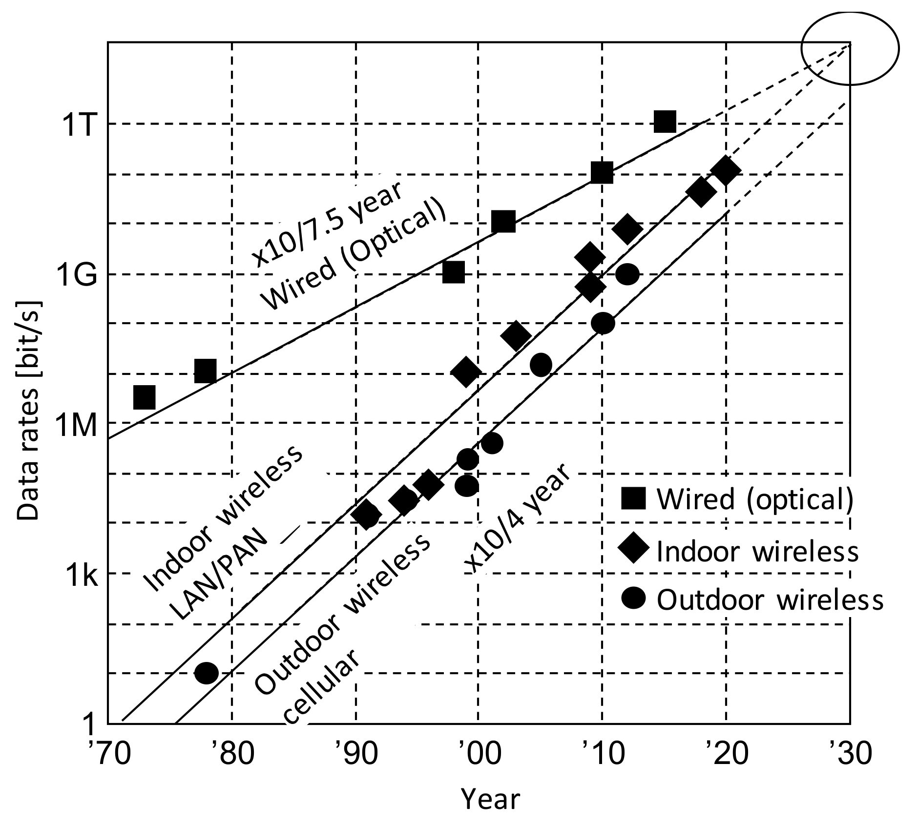
The data rate of communication has been increasing exponentially year-by-year, as shown in Figure 1 [1]. In particular, the improvement of the data rate of wireless communication has been remarkably rapid compared with wired communication. If the data rate continues to improve with this rate of advancement, rates of 100 gigabits per second—which cannot currently be realized except via optical communication—could be realized by wireless communication in 2020. In the field of ultra-high-speed wireless communication, wireless transceivers with data rates exceeding 100 gigabits per second have recently been released as if to support this. Extrapolating the graph as if this data rate growth will continue in the future allows the possibility that the wireless data rate will catch up with the wired data rate in 2030 [2]. Of course, there are many remaining technical challenges that will prevent wireless data rates catching up with the wired data rate, and equivalence cannot simply be realized. However, the era of low data rates in wireless communication will soon end.
The key to realizing wireless communication approaching wired data rates is the terahertz band, which has an intermediate property between radio waves and light with an electromagnetic wave around 1 THz. Terahertz wireless communication is one of the important applications covered by the terahertz photonics field [3]. Signals in this frequency band are generated and detected by photonics devices and electronic devices but, because of their significant technical difficulties, they are not yet widely used. However, communication using the terahertz band has attracted attention in recent years. This is because, unlike microwave and millimeter waves, the overwhelmingly wide frequency band near 100 GHz can be used. Such a wide frequency band is typically used in optical communication, in which high data rates have been realized, but has also become available for wireless communication.
The 300 GHz band corresponding to the low frequency band in the terahertz band is considered promising in wireless communication. Since this frequency band is included in the 220–330 GHz band of the WR-3 (3.4-inch rectangular waveguide, one of the specifications of a rectangular waveguide) waveguide standard, communication in this frequency band has been actively studied in recent years. In this paper, we will refer to communication using this WR-3 band as 300 GHz band communication.
Why is the 300 GHz band promising for communication? The most significant reason is the frequency allocation rule. Since radio waves are finite resources and the usage of each frequency is determined, the frequency band that can be used for communication is limited. Although a wide frequency band exists in the ultra-high frequency band higher than the millimeter wave, the frequency is allocated to various applications related to space observation, and it is difficult to use the continuous broadband for communication. A band of 252 GHz to 275 GHz has already been allocated to mobile and fixed wireless communications [4]. Further, a discussion on utilizing the frequency band exceeding 275 GHz, which is currently unallocated, for communication is underway within the International Telecommunication Union Radiocommunication Sector (ITU-R) [5]. Since the terahertz band has strong directivity and interference is not stringent, sharing of communication and observation is being considered. Therefore, the possibility of using the 300 GHz band for communication is increasing. As a result, it is expected that a continuous wide frequency band exceeding 252 GHz and extending over 275 GHz will be available soon for wireless communication.
In this paper, we discuss the silicon integrated circuit technology that realizes 300 GHz band communication, and new applications of terahertz communication, including using the 300 GHz band.
2. 300 GHz Band Transceiver Using Silicon Integrated Circuits
Here we introduce the features of silicon integrated circuits in comparison with compound semiconductor integrated circuits and introduce the technology of silicon integrated circuits which realizes a 300 GHz band communication transceiver.
2.1. Integrated Circuit Realizing Terahertz Transceiver and Its Characteristics
The frequency used for 300 GHz band communication is 100 times higher than that of widely used microwave communication. Therefore, it is necessary for the circuit to operate at ultra-high frequency. The realization of terahertz wireless communication has two approaches: all electronic and photonic-electronic hybrid. The latter covers the frequency band exceeding 500 GHz that is unachievable with the all-electronic approach, and which is desirable for downsizing and power reduction of the total communication system [6]. For this reason, the photonic-electronic hybrid approach has been studied previously to generate terahertz signals. However, research using integrated circuits, which is based on the all-electronic approach, has been undertaken recently. Integrated circuits are broadly classified into compound semiconductor integrated circuits using indium phosphide and gallium arsenide, and silicon integrated circuits fabricated on silicon substrates. In addition, silicon integrated circuits include silicon germanium (SiGe) BiCMOS (integrated circuits integrate bipolar-junction transistors and CMOS transistors in a single device) integrated circuits and CMOS integrated circuits. The difference between these integrated circuits is the maximum oscillation frequency of the transistor and the degree of integration. In accordance with Moore’s law, the performance of devices using compound semiconductors as well as silicon has been improved with the benefit of miniaturization. If capacitance and resistance are reduced by reducing the gate length (or base thickness) of the transistor, the high frequency performance is improved. The of the latest compound semiconductor transistor exceeds 1 THz [7,8], and of the SiGe bipolar transistor exceeds 500 GHz [9]. However, since the influence of the tunnel current and the variation due to the reduction of the power supply voltage becomes large, it is impossible to reduce the simple three-dimensional size, and the influence of the parasitic capacitance and the parasitic resistance prevents the high frequency performance of the transistor from being further improved. In the digital circuit, even if the performance of the transistor is not improved, the circuit performance is improved because the wiring length is shortened due to miniaturization of metal layers. On the other hand, of a transistor is important in a circuit handling high frequencies, especially terahertz frequencies. In the CMOS integrated circuit, remains at around 300 GHz after the 65 nm process, and the performance of the transistor is not significantly improved.
On the other hand, digital baseband logic can be integrated in BiCMOS integrated circuits and CMOS integrated circuits, whereas digital circuits cannot be integrated in compound semiconductor integrated circuits. In particular, large-scale digital circuits can be integrated in CMOS integrated circuits, which are becoming more miniaturized than BiCMOS circuits, so there is a possibility to realize a single chip terahertz transceiver device in the future. Although performance is inferior to that of compound semiconductors and SiGe integrated circuits, if the terahertz transceiver can be realized with CMOS integrated circuits, the application range will extend to portable devices.
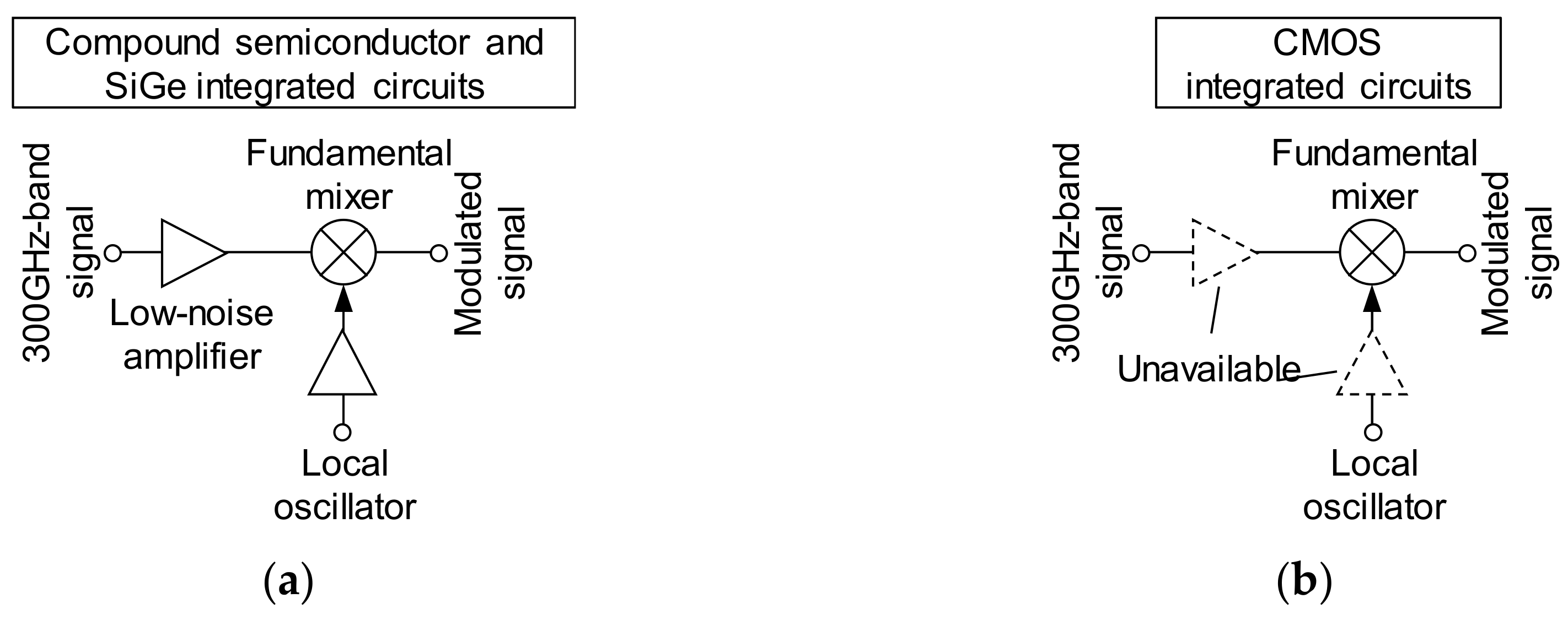
However, CMOS transceivers made of transistors with around 300 GHz cannot integrate power amplifiers in transmitters and low-noise amplifiers in receivers, which are generally essential for transceivers. As will be described later, it is the transmission power of the transmitter and the noise figure of the receiver that determines the communication performance, but the absence of the power amplifier and the low-noise amplifier is extremely disadvantageous in wireless communication. How can we overcome this disadvantageous condition? In the high-frequency front end of the transmitter or the receiver, the basic function is to convert the modulated baseband signal to the radio frequency signal. If an amplifier cannot be used, the mixer responsible for frequency conversion must be the last stage of the transmitter and the first stage of the receiver. As a result, performance improvement of this mixer is a key technology for realizing wireless transceiver under disadvantageous conditions. It is necessary to realize an ultrahigh-frequency circuit by a technology that does not rely on transistor miniaturization [10].
2.2. 300 GHz Band Transmitter Using Silicon Integrated Circuit
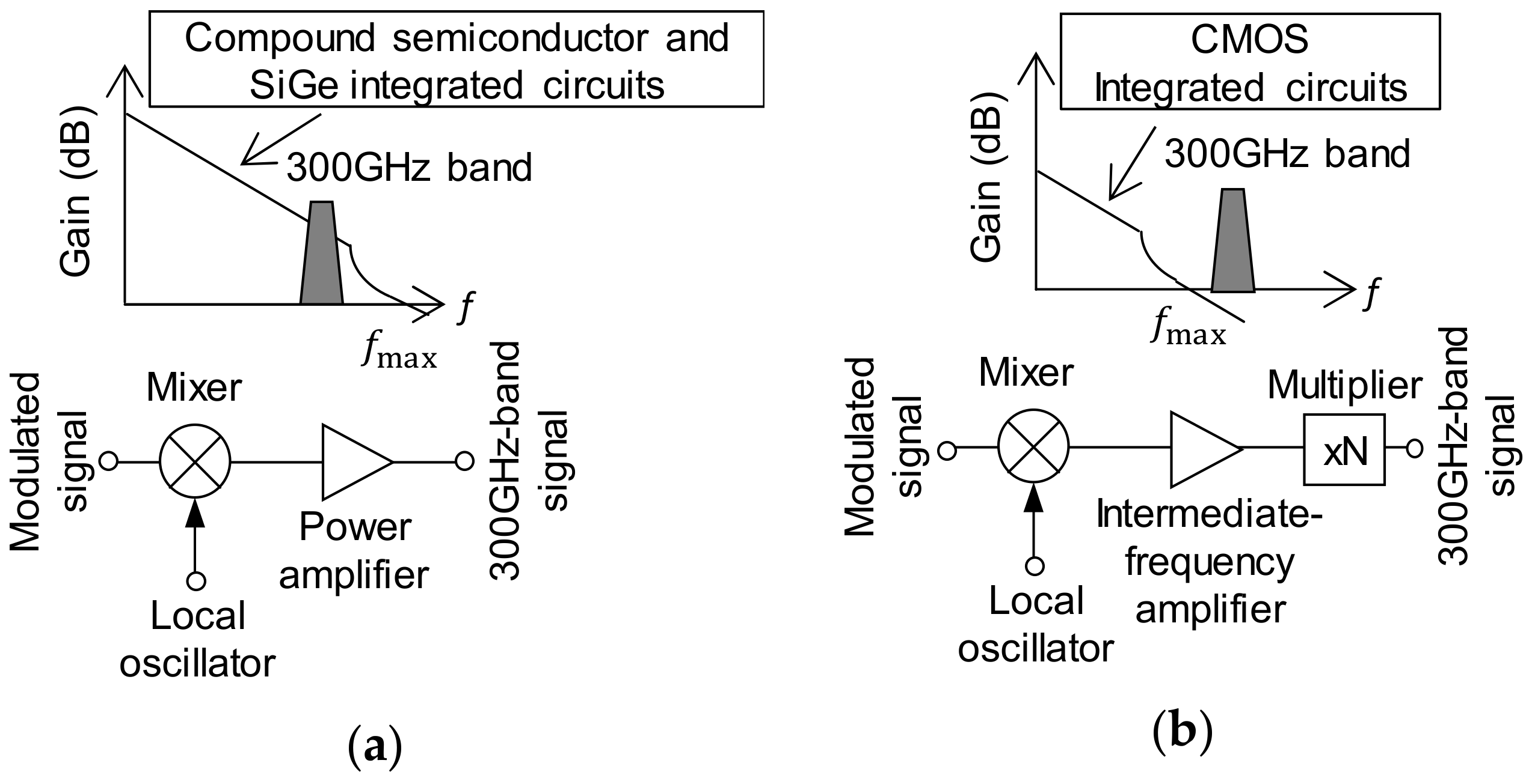
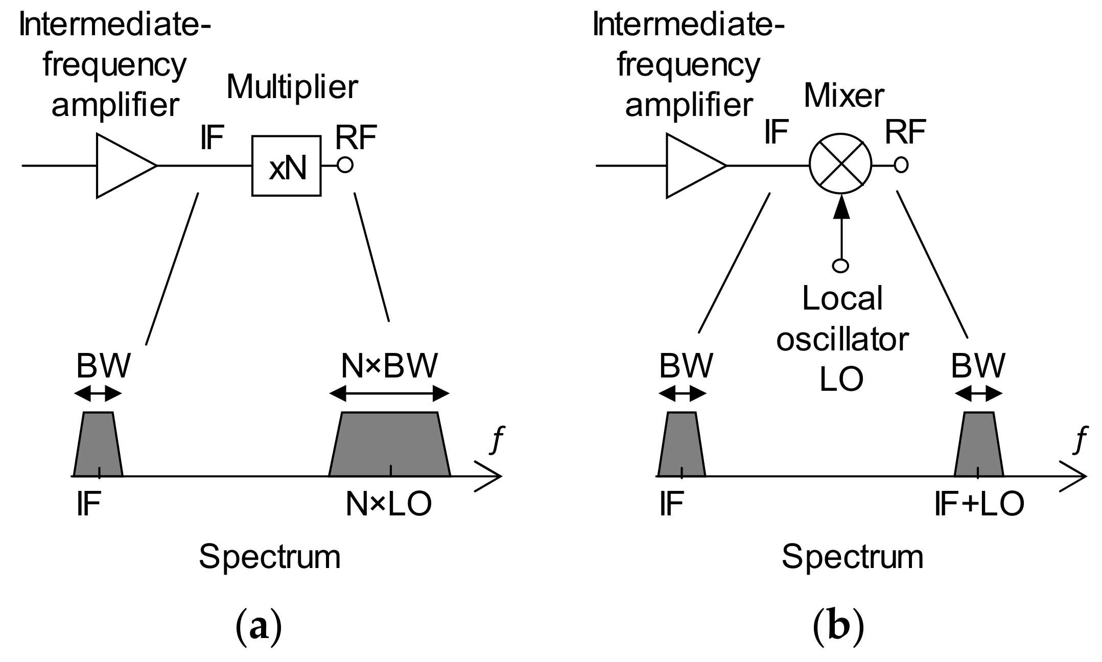
Even for the same silicon integrated circuit, the architecture of 300 GHz band transmitter differs according to . In the SiGe integrated circuit, as in the usual transceiver, as shown in Figure 2a, a power amplifier can be used for a 300 GHz band transmitter [11,12]. On the other hand, in CMOS integrated circuits, power amplifiers normally included in transceivers are not available. Therefore, to realize a 300 GHz band CMOS transmitter, a method shown in Figure 2b was proposed in which a modulated signal with an intermediate frequency of 80 GHz is multiplied by 3 in the final stage to generate a 240 GHz signal [13]. However, as shown in Figure 3a, not only the center frequency but also the frequency band expands three times in the multiplier, so the wide frequency band is not fully utilized even in the 300 GHz band. To fully utilize the wide frequency band, it is necessary to use a mixer for up-converting the center frequency without changing the frequency band (as shown in Figure 3b) at the final stage of the transmitter.
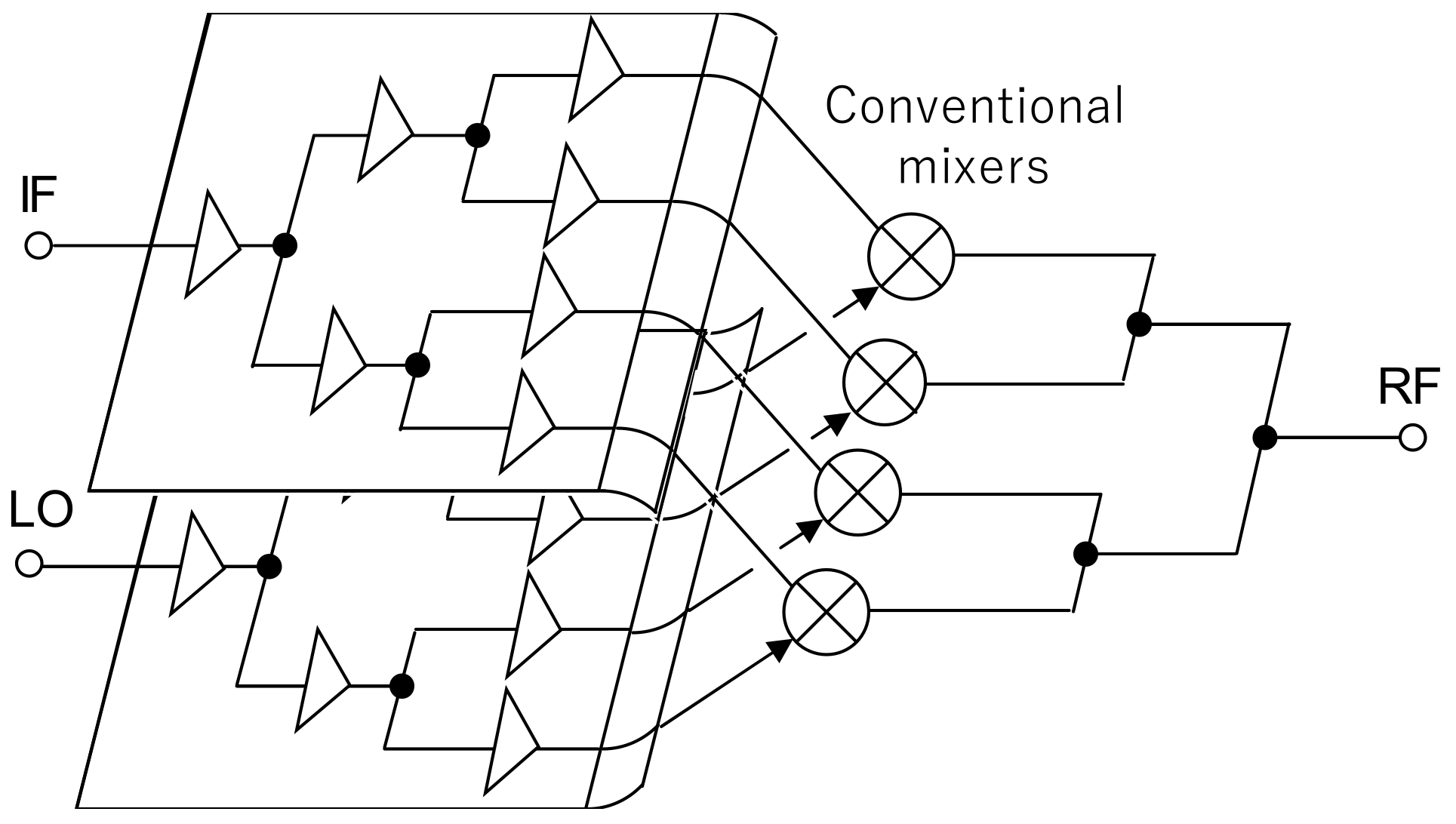
However, since the of the metal-oxide-semiconductor field-effect transistor (MOSFET) of the CMOS integrated circuit is low, the conversion gain of the mixer is below 0 dB and the output power is not large. It is noted that even if a power amplifier is not used, the output power can theoretically be increased when multiple mixers are connected in parallel for power combination. However, parallel connection of the mixers is not easy. This is because the mixer, which multiplies the frequency-converted signal by the local oscillation signal (LO), has two inputs and one output. These three signals must be divided and combined in parallel as shown in Figure 4 to connect mixers in parallel. When binary trees are used for each of the three input/output signal lines, the intersection of the signal lines necessarily occurs. This not only complicates the layout but also degrades the signal due to the intersection, so that performance improvement cannot be expected.
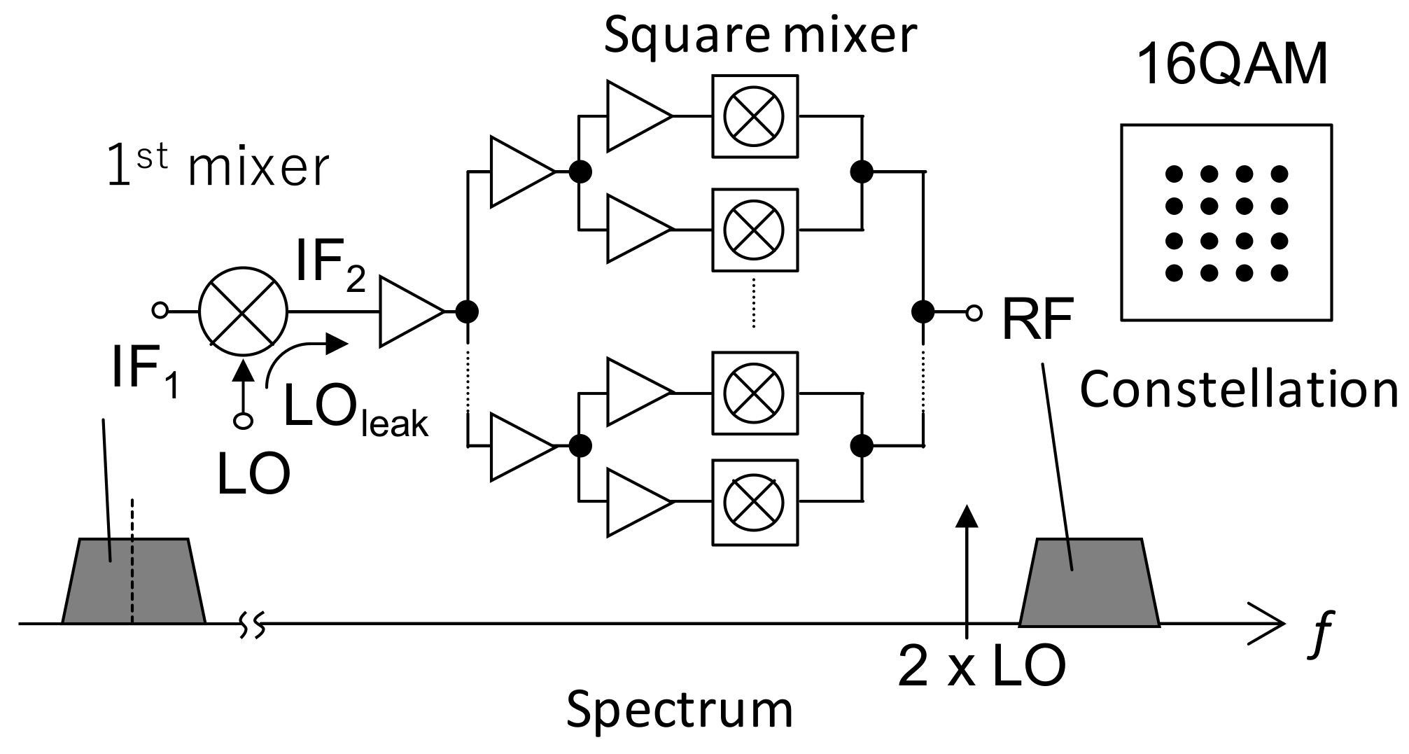
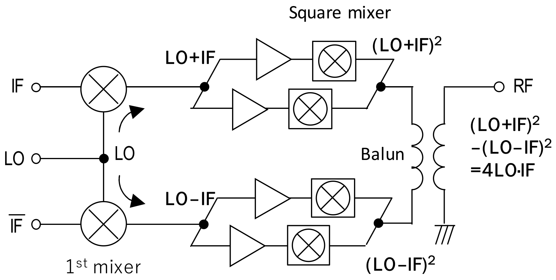
Therefore, in order not to degrade the signal, a mixer with two superimposed signals as the input at the final stage of the transmitter was used [14,15]. A frequency doubler circuit, called a square mixer since input signals are squared, is used for this mixer. Figure 5 shows the transmitter architecture using a square mixer [16]. If the frequencies of the two superimposed signals are close to each other, the two signals can be simultaneously amplified by the identical amplifier. It enables division and combination with a binary tree without complicating the layout. In the square mixer, the sum of the superimposed intermediate-frequency (IF) signal and the LO signal is squared. The generated output includes a desired signal which is the product of the two superimposed signals. On the other hand, besides the desired signal, an undesired signal consisting of the square of the IF signal and the square of the LO signal is simultaneously included. Since frequencies of these desired signals and undesired signals are close to each other, it is difficult to remove only undesired signals by using a bandpass filter. Therefore, as shown in Figure 6, two signal paths, an “” signal and an “” signal, are generated and given to the square mixer after being amplified. Then, these outputs are given to the balun. Finally, only the desired signal remains, and undesired signals are canceled by extracting the differential signal.
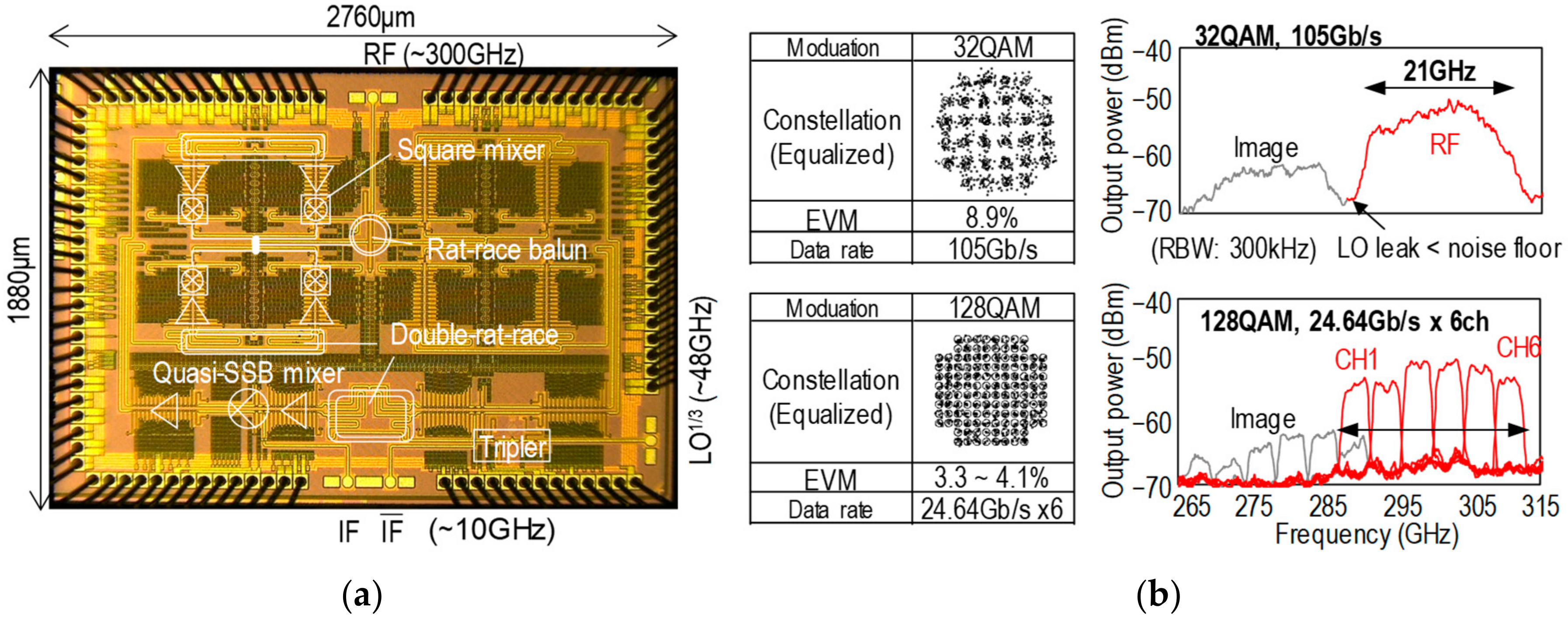
A 300 GHz band transmitter was fabricated in a 40 nm CMOS process. The chip micrograph of the transmitter and the measurement results are shown in Figure 7a. The fabricated 300 GHz band CMOS transmitter achieves a maximum data rate of 105 Gbit/s with 32 quadrature-amplitude modulation (QAM) at 21 Gbaud (gigabaud). With 128 QAM at 3.52 Gbaud, on the other hand, 24.64 Gbit/s can be generated using the 4.5 GHz frequency bandwidth. A graph superimposing spectrum obtained when six channels of signals of 4.5 GHz bandwidth are generated at different frequencies is shown in Figure 7b. As a result, the transmitter can generate a signal having a total bandwidth of 27 GHz (= 4.5 GHz × 6 channels) by limiting the channel band. This corresponds to 12.5 channels of the 2.16 GHz bandwidth used in the 60 GHz band. The maximum output power of the fabricated CMOS transmitter is dBm.
2.3. 300 GHz Band Receiver Using Silicon Integrated Circuit
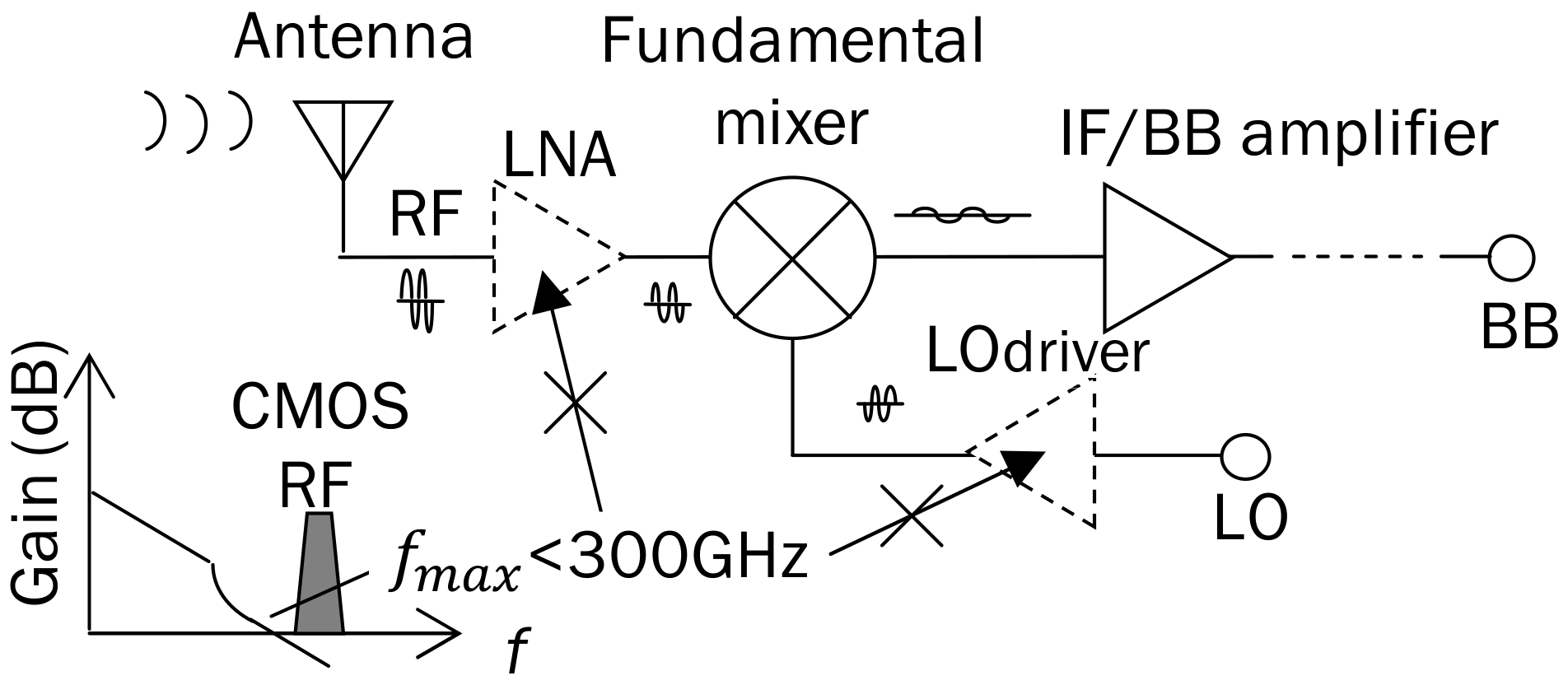
As shown in Figure 8a, the receiver of the SiGe integrated circuit can use a low-noise amplifier [11,12]. Furthermore, in recent receivers of SiGe integrated circuits, by using a 300 GHz band driver amplifier as an LO signal, it is possible to improve the conversion gain of the fundamental mixer and to remove the low-noise amplifier. As a result, conversion gain of +7 dB and a noise figure of 17 dB are realized without a low-noise amplifier [16]. In a receiver of a CMOS integrated circuit, however, since a low-noise amplifier cannot be used as shown in Figure 8b, the down conversion mixer must be used for the first stage. Figure 9 shows a block diagram of a 300 GHz band CMOS receiver [17,18]. How can the noise figure of the receiver be lowered without using a low-noise amplifier?
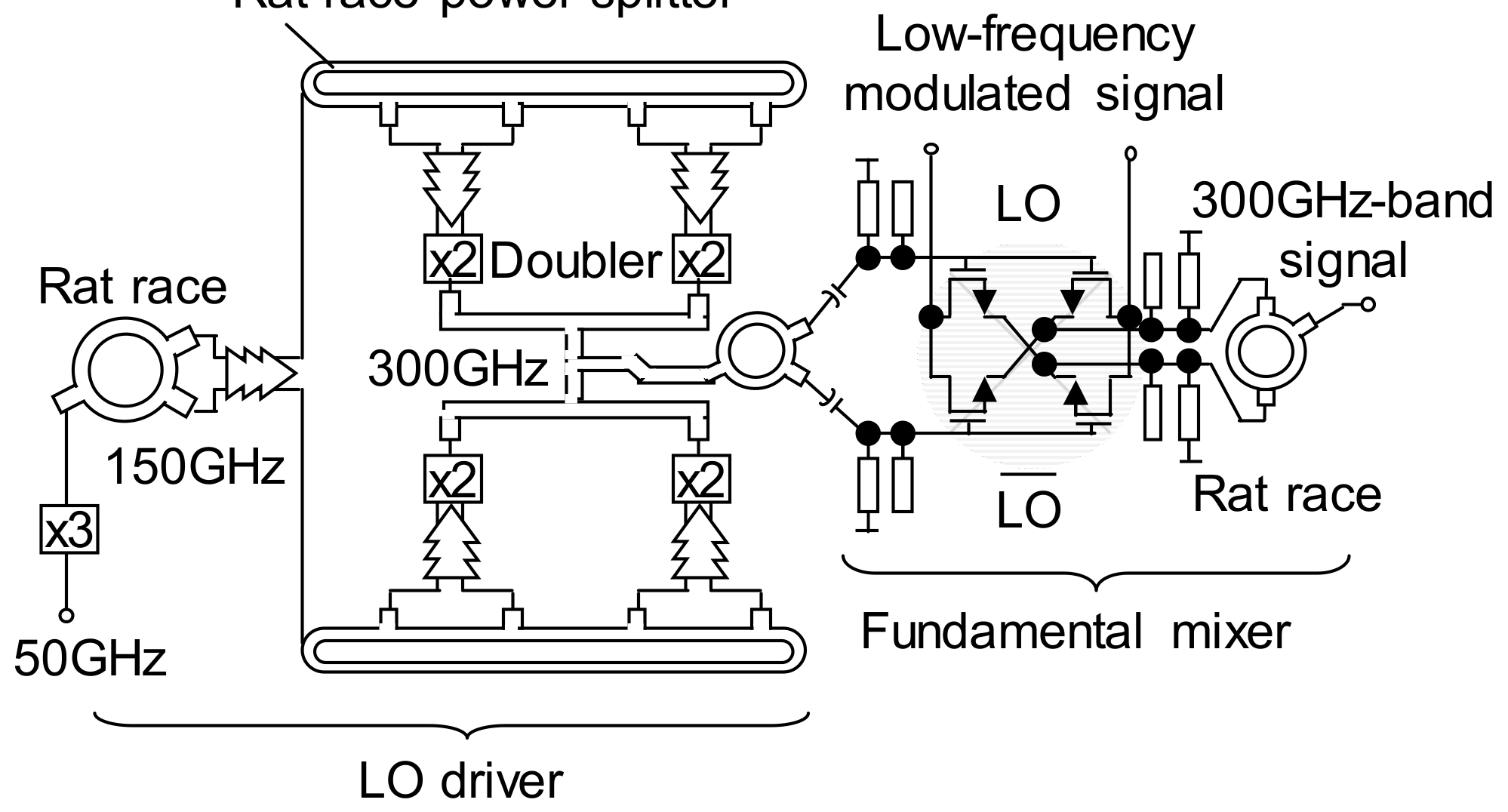
To lower the noise figure of the receiver, not only the noise figure but also the conversion loss of the first-stage mixer must be reduced. In general, harmonic mixers are often used for ultra-high frequency down-conversion mixers to lower the frequency of the LO. However, since a harmonic mixer has large conversion loss and high noise figure, performance of the receiver deteriorates. To suppress performance degradation of the receiver, it is necessary to use a fundamental mixer, in which the frequency of the local oscillator is the same as the input 300 GHz band. On the other hand, since the conversion gain of the mixer is proportional to the power of the LO, a LO with sufficiently large output is required to suppress the conversion loss. However, in CMOS integrated circuits, driver amplifiers for LO are unavailable. Therefore, the 300 GHz band CMOS receiver utilizes a LO generating the output power required for the fundamental mixer by parallel combination like the transmitter as shown in Figure 10 [17,18].
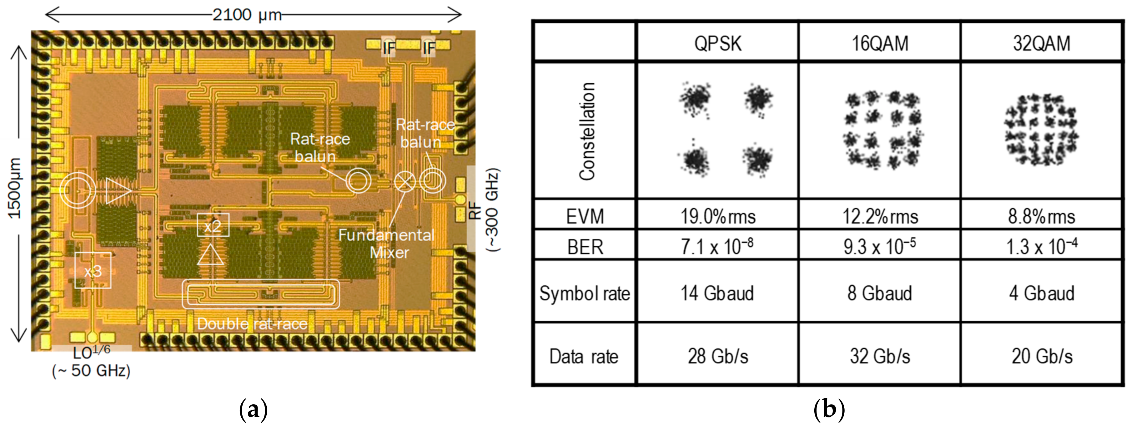
As with the transmitter, a 300 GHz band receiver was fabricated with a 40 nm CMOS process. The chip micrograph is shown in Figure 11a. The LO block occupies a large area of the chip by the parallel combiner. The measurement result of the receiving circuit is shown in Figure 11b. The modulation signal of the 300 GHz band given to the receiver was generated by the 300 GHz band CMOS transmitter shown in Figure 7. In the fabricated 300 GHz band CMOS receiver, the maximum data rate of 32 Gb/s is obtained at 16 QAM.
2.4. 300 GHz Band CMOS Transceiver Module
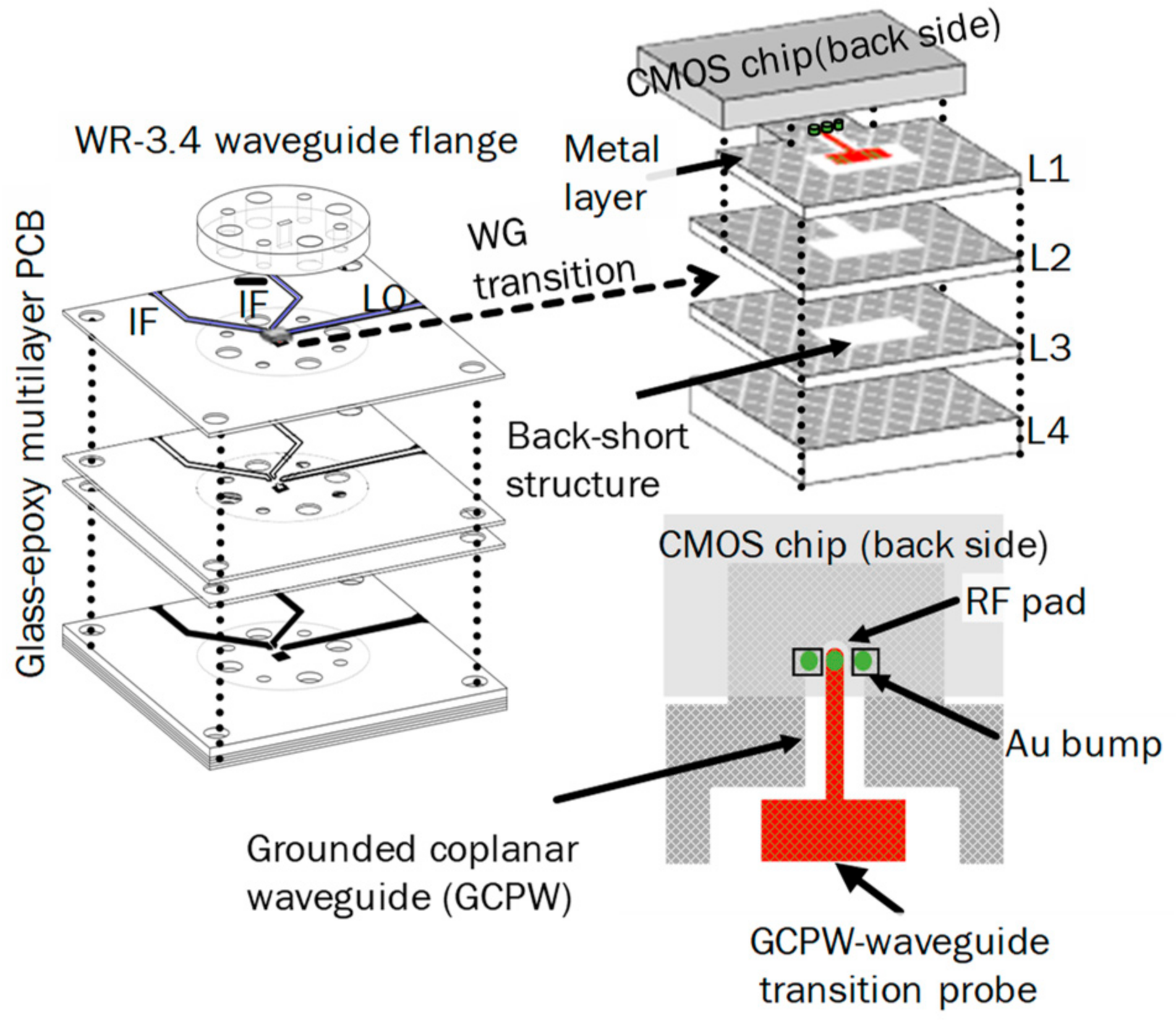
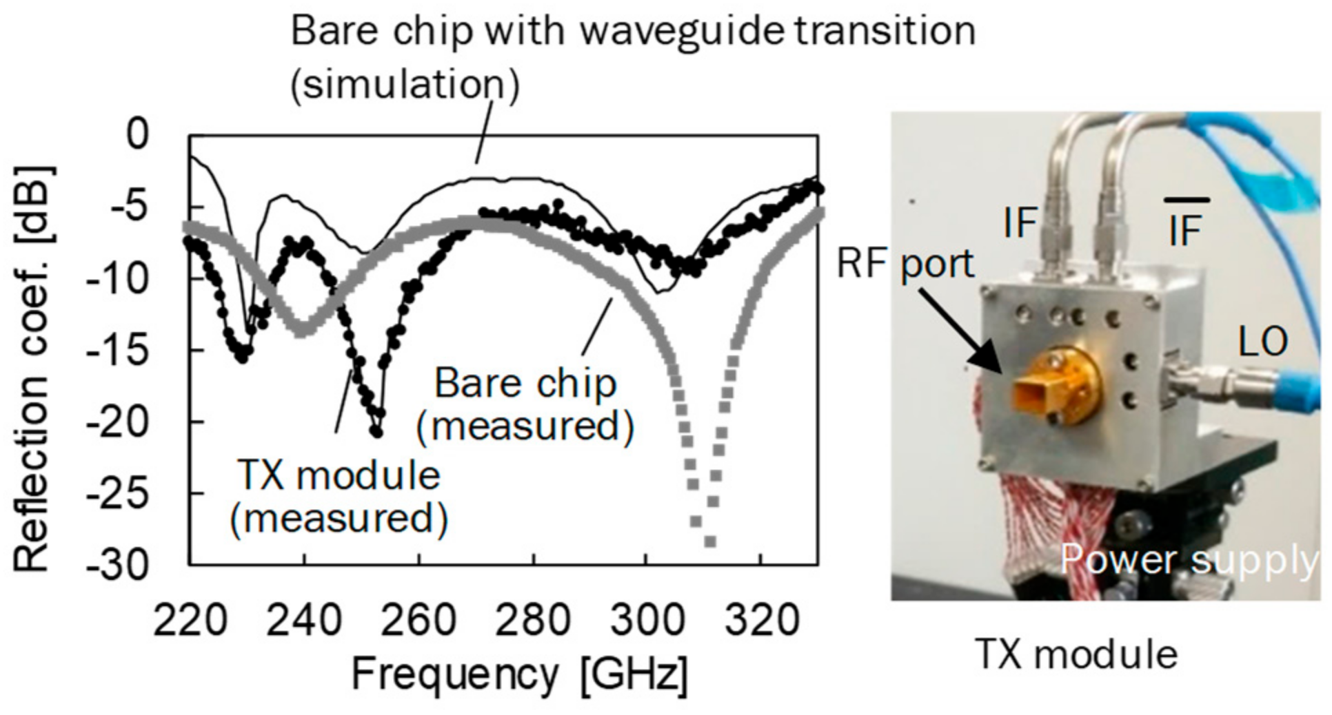
In Section 2.2 and Section 2.3, the technology of the CMOS integrated circuit that is the core of the 300 GHz band transceiver was introduced. In the measurement of the CMOS chip introduced in these sections, a waveguide probe attached to the wafer prober was used. Although wireless communication is possible by attaching an antenna to the waveguide probe, transceivers are not practical for wireless communication using a wafer prober. It is important to connect an antenna that converts space radio waves and electric signals in the CMOS chip without using a wafer prober and waveguide probes. Here, on-chip antennas are sometimes used for millimeter-wave CMOS transceivers [19]. However, the gain of the on-chip antenna is small, and its application is limited to short-distance wireless communication of several centimeters. On the other hand, it is necessary to use an antenna with high gain to extend the communication distance. Since the interface of the high gain antenna is generally a waveguide, an interface connecting the CMOS chip and the waveguide is required. In consideration of practical application, a CMOS-to-waveguide interface is proposed using a conventional multi-layer glass epoxy printed board as shown in Figure 12 [20]. The CMOS chip is flip-chip mounted on a multilayer printed circuit board. The 300 GHz band signal generated by the CMOS chip is transmitted using a microstrip line as short as 200 μm on the printed circuit board. A waveguide conversion probe similar in shape to the patch antenna was formed at the tip of the microstrip line. A quarter wavelength back-short structure required for waveguide conversion was formed in the multilayer substrate and a metal waveguide flange was mounted on the surface of the printed circuit board. This realizes CMOS waveguide conversion.
Figure 13 shows the reflection characteristics at the opening of the waveguide flange and the photograph of the module. CMOS waveguide conversion using a printed circuit board was realized. However, the minimum value of the reflection characteristic shifts downward from 300 GHz to 250 GHz due to the estimation errors in the material constant of the substrate and the output reflection characteristic of the CMOS chip.
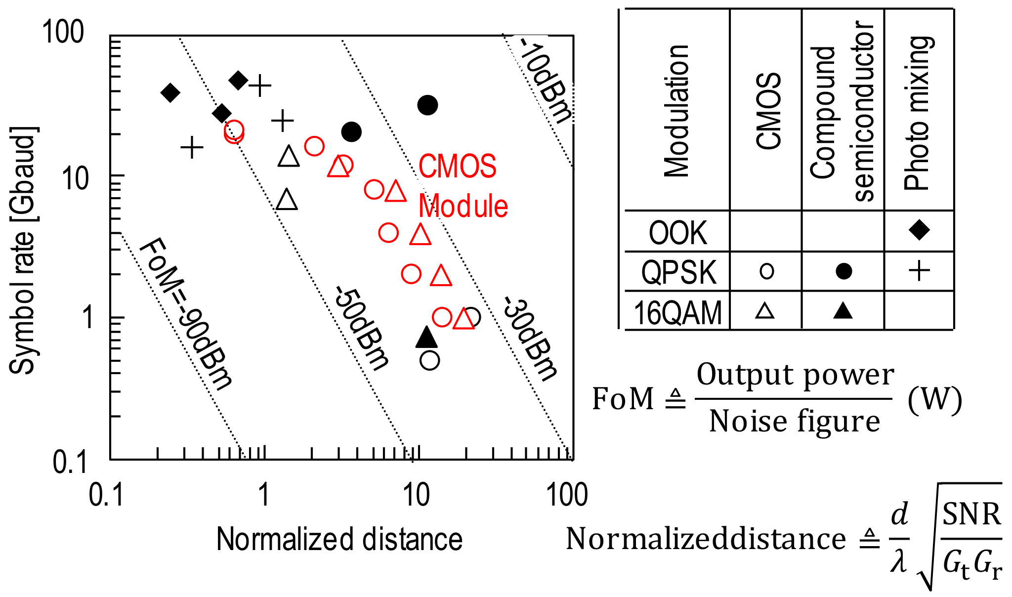
Experiments of wireless communication were carried out using the fabricated CMOS transmission module. To compare and evaluate the performance of this module, it is necessary to compare with the result of other terahertz communication experiment. On the other hand, in each piece of communication experiment, it is not valid to simply compare the data rate and the communication distance because the modulation scheme, antenna gain, frequency (wavelength), and allowable bit error rate are different. The communication distance in which these parameters are normalized [20,21] is:
where is the communication distance, is the wavelength, is the signal-to-noise ratio of the receiver, and and are the antenna gain of the transmitter and the receiver, respectively. By using , the noise power spectral density ( dBm/Hz) and the symbol rate , the figure of merit () is
The is determined by the ratio between the transmission power and the noise figure of the receiver. The comparison result is shown in Figure 14. The results of the communication experiment using our CMOS transmitter are not inferior to the results using other compound semiconductors.
3. Features and Applications of 300 GHz Band Communication
Practical application of terahertz communication depends on communication characteristics, including communication distance. Therefore, we first consider its characteristics and suitable applications. Then, we introduce recently standardized channel allocation in the 300 GHz band, and finally consider the possibility of application to space.
3.1. Characteristics of Terahertz Band Communication
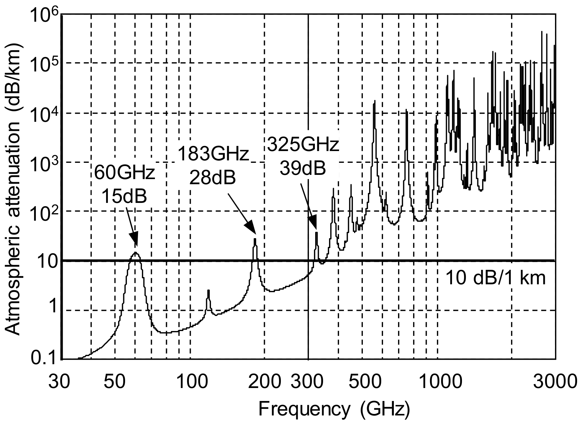
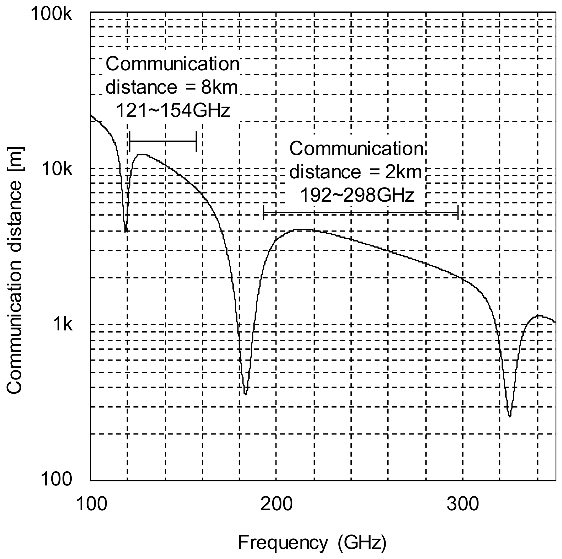
You may imagine that the terahertz band has a large atmospheric attenuation and is limited to near-field communication. How large is the effect of atmospheric attenuation? Figure 15 shows atmospheric attenuation from 30 GHz to 3 THz [22,23]. If the atmospheric attenuation is less than 10 dB, the effect is relatively small. On the other hand, for example, if the atmospheric attenuation at 1 km exceeds 10 dB, kilometer-class communication may become difficult. Such frequencies are 60 GHz, 183 GHz, 325 GHz and above 351 GHz. Apart from these frequency bands, the influence of atmospheric attenuation is relatively small for medium-range communications of at least about 1 km. In Figure 16, to estimate the communication distance, the distance at which the atmospheric attenuation is 10 dB is shown. There is a wide radio-wave window with a communication distance of 2 km from 192 GHz to 298 GHz [24]. This is one reason why the 300 GHz band is attracting attention as a communication application.
On the other hand, it is necessary to consider free space propagation loss besides atmospheric attenuation. Using received power , transmit power , transmitter antenna gain , receiver antenna gain , wavelength , and communication distance , propagation loss is given by:
Equation (3) is known as the Friis transmission equation. According to (3), as the wavelength decreases, the received power decreases and the propagation loss increases. On the other hand, if the effective areas of the transmitting and receiving antennas are and respectively, the antenna gain is given by:
The antenna gain is proportional to the effective area and increases in inverse proportion to the square of the wavelength . Substituting (4) and (5) into (3) gives:
Equation (6) is nothing other than the equation shown in Friis’ original paper [25]. Equation (6) shows that if the effective area of the antenna is constant, the received power increases in inverse proportion to the square of the wavelength, and the propagation loss decreases. In terahertz communication, it is important not to reduce the antenna area to realize medium to long distance transmission. Since the antenna gain increases as the frequency increases with the antenna area constant, terahertz communication is more suitable for one-to-one communication than broadcasting.
3.2. Application Examples of 300-GHz-Band Communication
Since the data rate equivalent to optical communication can be realized in the 300 GHz band, PAR (Project Application Request) of IEEE 802.15.3d shows application examples for replacing optical communication with wireless communication, such as a wireless backhaul/fronthaul, intra-device wireless communication, point-to-point switch connections for data centers, and proximity wireless applications including kiosk download [26].
On the other hand, low latency is one of the advantages of wireless communication over optical communication. The propagation velocity of the electromagnetic wave is inversely proportional to the square root of the dielectric constant of the medium. For this reason, the propagation speed of atmospheric electromagnetic waves is about 50% faster than that of optical fibers, and wireless communication is excellent for real-time applications. Utilizing this property, a microwave line dedicated to high-speed trading was laid at a cost of USD 250 million between New York and Chicago [27]. In terahertz communication, the same communication capacity can be transmitted as optical communication with low latency. In the case of 8K video images, which will be broadcast in Japan in 2018, communication capacity of up to 144 gigabits per second for uncompressed streaming is required. 144 gigabit per second wireless communication can be realized with 16 QAM and a roll-off coefficient of 0.25 when a bandwidth of 45 GHz is available. This frequency bandwidth can be allocated in the 300 GHz band. For example, by using a drone equipped with an 8K camera, the situation of a disaster site or a distress location can be quickly observed in real time. This is a new application which cannot be realized by conventional microwave communication or optical communication.
3.3. Application Example of 300 GHz Band Communication
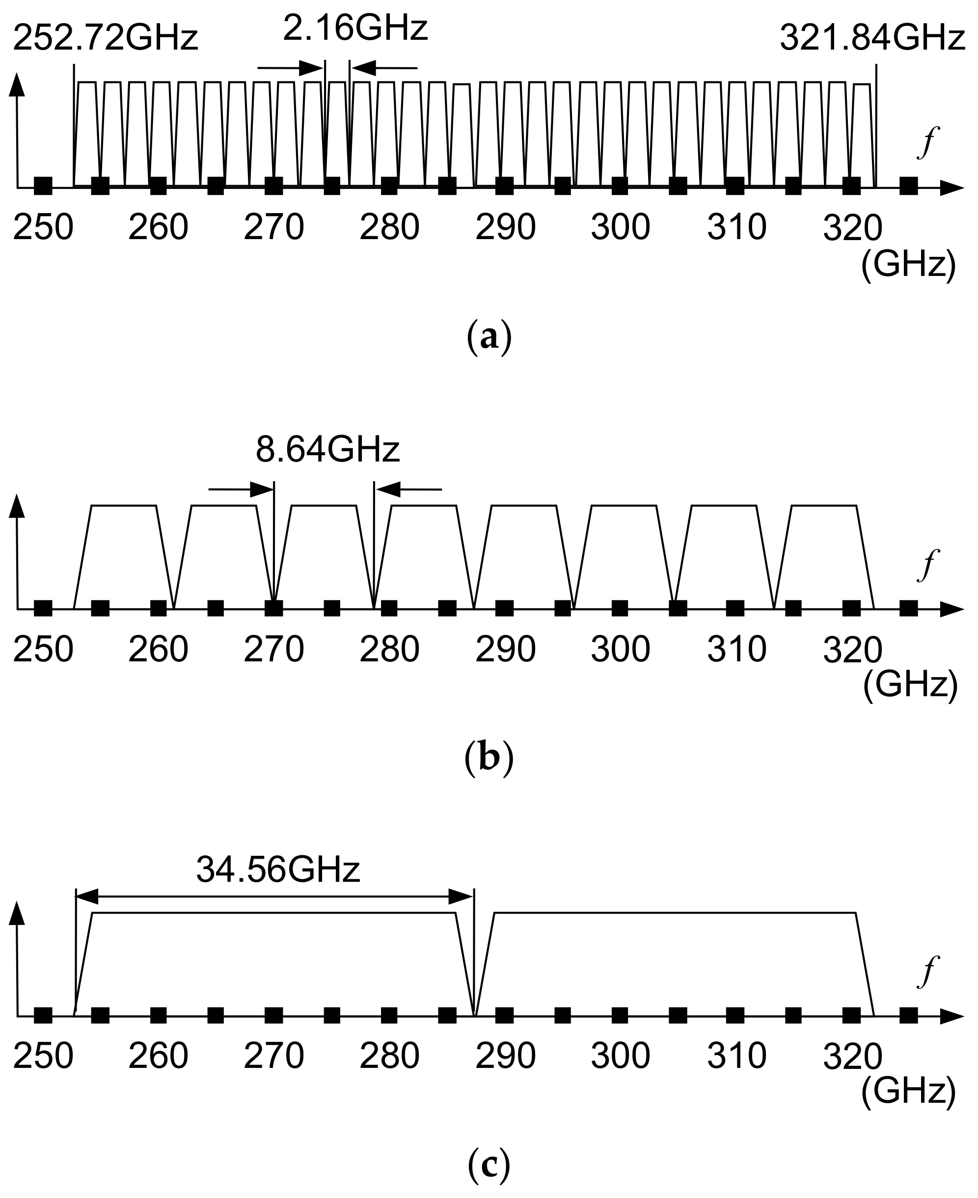
In IEEE 802.15.3d, the standard for channel allocation in the 300 GHz band has been established [28]. In this standard, channels are allocated to frequency bands close to 70 GHz from 252 GHz to 321 GHz (Figure 17), which are composed of frequencies already allocated for communication and frequencies expected to be allocated to communication in the future. To maintain compatibility with the conventional 60 GHz band standard, a plurality of channel bands that are multiples of 2.16 GHz, as shown in Figure 17a,b, are allocated to this frequency band. On the other hand, considering that the data rate of wireless communication is close to optical communication, it is preferable to consider compatibility with wired communication standards. For example, the 28 Gbit/s standard is widely used in NRZ (non-return to zero) transmission called CEI-28G (Common Electrical Interface 28 Gigabit-per-second) for electrical interfaces of FPGAs (field programmable gate arrays) and optical fiber. Assigning these two NRZ signals to the I/Q signals used for quadrature phase shift keying (QPSK) results in 56 Gbit/s wireless communication. Since the symbol rate is 28 Gbaud (gigabaud), when it is modulated with a roll-off coefficient of 0.2, it becomes a bandwidth of 33.4 GHz. According to the IEEE 802.15.3 d standard, a channel suitable for this band is not currently defined. However, allocating 34.56 GHz, which is 16 times 2.16 GHz, to one channel is suitable for connecting the 28 Gbps NRZ wired signal to the 56 Gbps QPSK radio signal. As long as the channel bandwidth is 34.56 GHz, as shown in Figure 17c, two channels can be allocated to the entire frequency band specified by IEEE 802.15.3 d. Assigning channels in this way, the channel on the low frequency side from 252 GHz to 287 GHz has a long distance of about 2 km as the atmospheric attenuation becomes 10 dB, which is suitable for medium- to long-distance communication.
3.4. The Future of Terahertz Communication Spreading in Space
Inter-server communication for data centers, backhaul and fronthaul of networks, and high-speed communication in electronic devices are assumed applications of terahertz communication but these are forms of fixed wireless communication that have been realized by the conventional optical fiber network. Merely replacing fixed communication, however, does not achieve the maximum potential of terahertz communication. On the other hand, since terahertz air attenuation is large, it may be thought that it is unsuitable for long distance communication. However, as mentioned in Section 2, there is an atmosphere window in the 300 GHz band. In addition, if the antenna size is maintained, even if the wavelength is short, the directivity increases but the propagation loss decreases. The received power increases as the frequency increases if the effective area of the antenna is constant, so ultra-high-speed terahertz communication may be utilized in the universe without atmospheric attenuation if a high-power terahertz transmitter and a high-gain antenna are available. In the 300 GHz band, the gain of a parabola antenna with a 1.2-m diameter will be 70 dBi from Equation 5 if the aperture efficiency is 70%. The diameter of the beam produced by the antenna with the gain at the distance is given by:
regardless of the frequency. With a 70 dBi antenna, the diameter of the beam 1000 km ahead will be 1.3 km. Terahertz communication in which the beam diameter is wider than the laser beam helps alleviate the requirement of position control of the antenna. Furthermore, in the terahertz communication in the universe without atmospheric attenuation, a frequency band exceeding 300 GHz can be utilized. Although not in the 300 GHz band, as shown in Figure 16, in the frequency band from 121 GHz to 154 GHz, the distance at which the atmospheric attenuation becomes 10 dB exceeds 8 km. If this wide frequency bandwidth that is not currently allocated to communication is available, stable high-speed communication to the universe is possible in the desert without rain attenuation located at an altitude of 5000 m at which the air density is about half that of the sea level.
In the future, can we use terahertz communication to solve social problems? For example, to simulate various phenomena in the real world accurately on a large scale, it is indispensable to improve the performance of supercomputers. What are the challenges that must be solved when performance improvement of supercomputers is expected in the future? The computing performance of the supercomputer has improved exponentially, by 1000 times in about 10 years [29]. Currently, development is progressing toward the realization of an exascale computer that performs floating-point calculations times per second in 2020. If the computation speed continues to improve after 2020, a zettascale computer will be created in 2030 that will perform floating point calculations at a tremendous rate of times per second. One problem here is power consumption. It is foreseen that the power consumption of an exascale computer will be 20 MW [29]. On the other hand, in a zettascale computer with 1000 times higher computing capacity, the power consumption will be 20 GW if the hardware scale is simply multiplied by 1000. Even if low-power technology is developed, the power consumption of the zettascale computer will be around 1 GW. The power consumption of 1 GW is roughly equivalent to the output of one nuclear power generator. How can we maintain a sustainable society while covering the enormous power consumption of such supercomputers? Research on space photovoltaic power generation using a 2.5-km-square solar panel on a geostationary orbit is proceeding as one of stable candidates for renewable energy [30]. This solar panel can generate 1 GW. Electricity produced by space photovoltaic power will be transmitted to the ground using microwaves. The target efficiency of power transmission is 50%. If a supercomputer is built together with the space photovoltaic panel, and electric power generated by space photovoltaic power is used in place, power can be effectively utilized without transmission loss [30]. Ultra-high-speed terahertz communication can be used for large-volume data exchange for space supercomputers that cannot lay optical fiber.
On the other hand, it will be an era of monitoring the real world with enormous sensors exceeding 1 trillion units and processing that information with artificial intelligence. Although the information obtained from the sensor cannot be stored as it is, the amount of stored data will exponentially increase. On the other hand, cold data in which access frequency decreases with time will also increase. Since the access frequency of cold data is low, the access speed is not important. When slow access is allowed, it may be possible to construct a cold storage data center on the moon, for example, rather than on Earth [31]. Since the light propagation time to the moon is 1.3 s, the access speed will be about 3 s in a round trip. Nonetheless, a lunar cold storage data center will be one of the candidates for utilization on the moon.
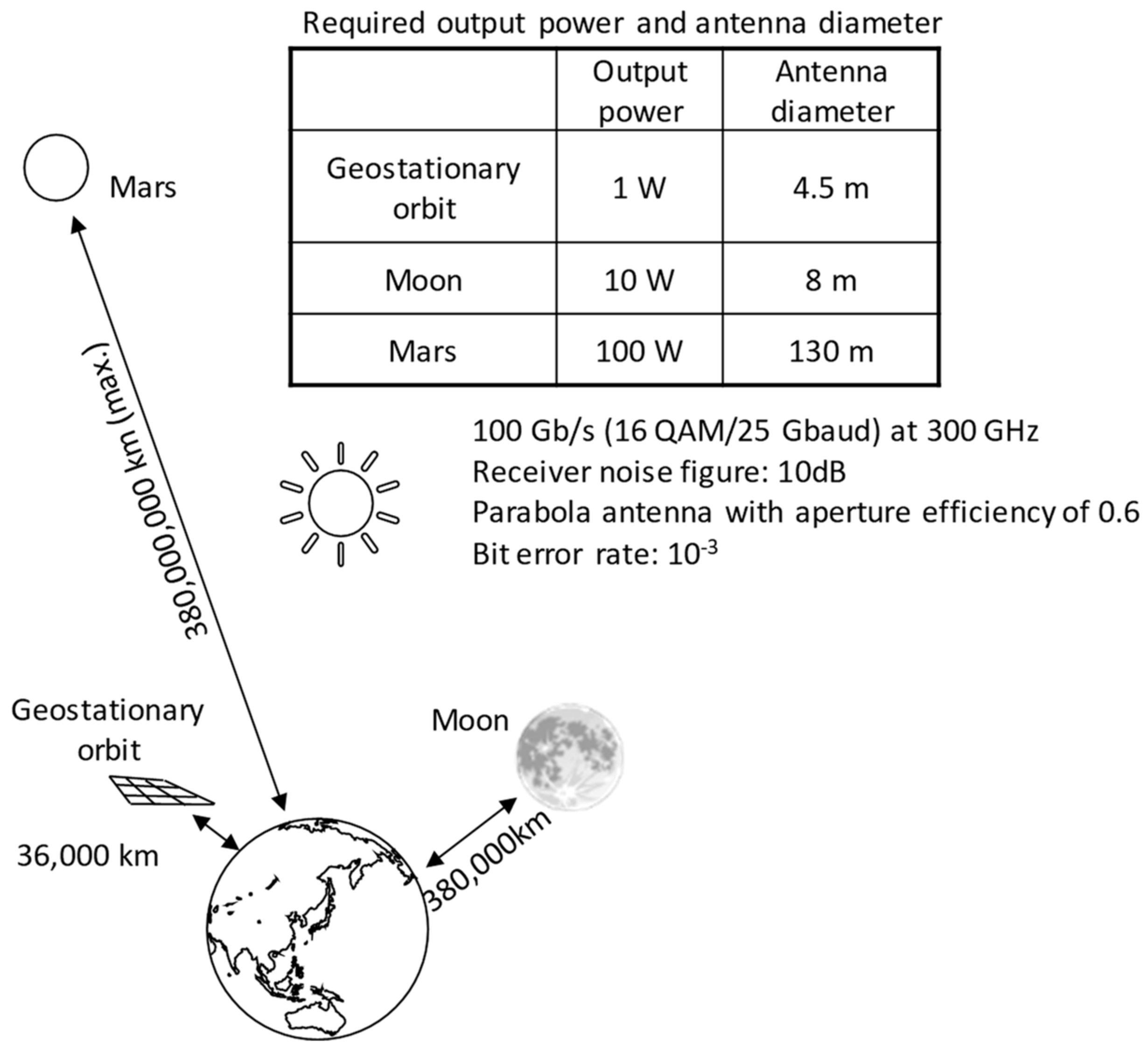
Furthermore, manned exploration of Mars and migration of mankind are currently being studied [32]. The means of communication of the migrants to Mars is limited to radio. It is noted that one petabyte can be transmitted per day when information can be sent at a data rate of 100 gigabits per second. When Mars is furthest from Earth it takes 21 min to propagate electromagnetic waves. Hence, although communication will not be real time, terahertz communication makes it possible to exchange large volumes of information between Earth and Mars.
It is noted that the moon’s atmosphere is very low (i.e., almost vacuum). The atmospheric pressure of Mars is about 0.6% of the Earth, and most of the atmosphere is carbon dioxide. Carbon dioxide absorbs infrared to cause a greenhouse effect but does not absorb terahertz. Therefore, terahertz absorption on the moon and Mars is negligible. Performance required for achieving terahertz communication with geostationary orbits of the moon and Mars is estimated in Figure 18. Although it may not be a technology that can be realized immediately, the space utilization of ultra-high-speed terahertz communication will be a meaningful challenge to overcome for the sustainable development of mankind.
4. Conclusions
Since atmospheric attenuation is relatively small in the 300 GHz band, it is the last remaining frequency band where a wide frequency band near 70 GHz can be used. It was shown that a 300 GHz band transmitter and receiver can be realized with a silicon CMOS integrated circuit with lower frequency performance than of a compound semiconductor. When a commercial CMOS baseband signal processor for optical communication is combined with a terahertz front end, terahertz communication can be put to practical use at an early stage. However, the performance of a terahertz transceiver using a CMOS integrated circuit is still insufficient. It is necessary to further improve the performance by combining a power amplifier and a low-noise amplifier with a compound semiconductor with a CMOS integrated circuit. A traveling-wave tube is also conceivable for applications requiring watt-class power [33]. Heterogeneous integration of CMOS integrated circuits with compound semiconductors and traveling wave tubes may be the key to solving future challenges.
High-power signals have been generated in the UHF band since the first magnetron was invented in 1921, and research on microwaves such as radar became popular. Fifty years after the invention of the magnetron, in 1970, single mode fiber was invented, and optical communication was subsequently actively studied. As a result, large-volume long-distance transmission became possible, and society changed drastically. There are signs that terahertz communication will open up a new world in a further 50 years hence, in 2020. Wireless communications in the 300 GHz band that can realize the same data rates as wired communications have the potential to affect space plans after 2020. The ability of terahertz communication to connect places that cannot be connected by wired communication, and enabling the same volume as optical communication, will significantly change the society of the future.
Funding
The research results on the 300 GHz band CMOS transceiver was partially supported by the Ministry of Internal Affairs and Communications.
Acknowledgments
Applications of terahertz communication include contents obtained through discussions with Dr. Hosako of the National Institute of Information and Communications Technology (NICT). We thank the members of NICT, Panasonic and Hiroshima University participating in this project.
Conflicts of Interest
The authors declare no conflict of interest.
References
- Kürne, T. IEEE 802.15-10-0320-02-0000-Tutorial_Igthz. Available online: https://mentor.ieee.org/802.15/dcn/12/15-12-0320-02-0thz-what-s-next-wireless-communication-beyond-60-ghz-tutorial-ig-thz.pdf (accessed on 21 November 2018).
- Fujishima, M. Silicon integrated circuits creating new applications in terahertz communication. J. IEICE 2018, 101, 554–560. (In Japanese) [Google Scholar]
- Tonouchi, M. Cutting-edge terahertz technology. Nat. Photonics 2007, 1, 97–105. [Google Scholar] [CrossRef]
- International Telecommunication Union. Article 5: Frequency allocations. In Radio Regulations Article Edition of 2012; International Telecommunication Union (ITU): Geneva, Switzerland, 2012; pp. 37–178. Available online: http://search.itu.int/history/HistoryDigitalCollectionDocLibrary/1.41.48.en.101.pdf (accessed on 21 November 2018).
- Resolution 767, The World Radiocommunication Conference (Geneva, 2015). Available online: https://www.itu.int/dms_pub/itu-r/oth/0c/0a/R0C0A00000C0016PDFE.pdf (accessed on 21 November 2018).
- Nagatsuma, T.; Ducournau, G.; Renaud, C.C. Advances in terahertz communications accelerated by photonics. Nat. Photonics 2016, 10, 371–379. [Google Scholar] [CrossRef] [Green Version]
- Deal, W.R.; Zamora, A.; Leong, K.; Liu, P.H.; Yoshida, W.; Zhou, J.; Lange, M.; Gorospe, B.; Nguyen, K.; Mei, X.B. A 670 GHz low noise amplifier with <10 dB packaged noise figure. IEEE Microw. Wirel. Compon. Lett. 2016, 26, 837–839. [Google Scholar]
- Kallfass, I.; Boes, F.; Messinger, T.; Antes, J.; Inam, A.; Lewark, U.; Tessmann, A.; Henneberger, R. 64 Gbit/s transmission over 850m fixed wireless link at 240 GHz carrier frequency. J. Infrared Millim. Terahertz Waves 2015, 36, 221–233. [Google Scholar] [CrossRef]
- Fox, A.; Heinemann, B.; Rücker, H.; Barth, R.; Fischer, G.G.; Wipf, C.; Marschmeyer, S.; Aufinger, K.; Böck, J.; Boguth, S.; et al. Advanced heterojunction bipolar transistor for half-THz SiGe BiCMOS technology. IEEE Electron Device Lett. 2015, 36, 642–644. [Google Scholar] [CrossRef]
- Fujishima, M.; Amakawa, S. Recent progress and prospects of terahertz CMOS. IEICE Electron. Express 2015, 12, 20152006. [Google Scholar] [CrossRef]
- Kim, S.; Yun, J.; Yoon, D.; Kim, M.; Rieh, J.-S.; Urteaga, M.; Jeon, S. 300 GHz integrated heterodyne receiver and transmitter with on-chip fundamental local oscillator and mixers. IEEE Trans. Terahertz Sci. Technol. 2015, 5, 92–101. [Google Scholar] [CrossRef]
- Sarmah, N.; Grzyb, J.; Statnikov, K.; Malz, S.; Vazquez, P.R.; Föerster, W.; Heinemann, B.; Pfeiffer, U.R. A fully integrated 240-GHz direct-conversion quadrature transmitter and receiver chipset in SiGe technology. IEEE Trans. Microw. Theory Techn. 2016, 64, 562–574. [Google Scholar] [CrossRef]
- Kang, S.; Thyagarajan, S.V.; Niknejad, A.M. A 240 GHz fully integrated wideband QPSK transmitter in 65 nm CMOS. IEEE J. Solid-State Circuits 2015, 50, 2256–2267. [Google Scholar] [CrossRef]
- Katayama, K.; Takano, K.; Amakawa, S.; Hara, S.; Kasamatsu, A.; Mizuno, K.; Takahashi, K.; Yoshida, T.; Fujishima, M. A 300 GHz CMOS transmitter with 32-QAM 17.5 Gb/s/ch capability over six channels. IEEE J. Solid-State Circuits 2016, 51, 3037–3048. [Google Scholar] [CrossRef]
- Takano, K.; Amakawa, S.; Katayama, K.; Hara, S.; Dong, R.; Kasamatsu, A.; Hosako, I.; Mizuno, K.; Takahashi, K.; Yoshida, T.; et al. A 105Gb/s 300GHz CMOS transmitter. In Proceedings of the 2017 IEEE International Solid-State Circuits Conference (ISSCC), San Francisco, CA, USA, 5–9 February 2017; pp. 308–309. [Google Scholar]
- Vazquez, P.; Grzyb, J.; Sarmah, N.; Heinemann, B.; Pfeiffer, U. A 219-266 GHz fully-integrated direct-conversion IQ receiver module in a SiGe HBT technology. In Proceedings of the 12th European Microwave Integrated Circuits Conference, Nuremberg, Germany, 8–10 October 2017; pp. 261–264. [Google Scholar]
- Hara, S.; Katayama, K.; Takano, K.; Dong, R.; Watanabe, I.; Sekine, N.; Kasamatsu, A.; Yoshida, T.; Amakawa, S.; Fujishima, M. A 416-mW 32-Gbit/s 300-GHz CMOS receiver. In Proceedings of the 2017 IEEE International Symposium on Radio-Frequency Integration Technology (RFIT), Seoul, Korea, 30 August–1 September 2017; pp. 65–67. [Google Scholar]
- Hara, S.; Katayama, K.; Takano, K.; Dong, R.; Watanabe, I.; Sekine, N.; Kasamatsu, A.; Yoshida, T.; Amakawa, S.; Fujishima, M. A 32 Gbit/s 16QAM CMOS receiver in 300 GHz band. In Proceedings of the 2017 IEEE International Microwave Symposium (IMS2017), Honolulu, HI, USA, 4–9 June 2017; pp. 1–4. [Google Scholar]
- Park, J.; Kang, S.; Thyagarajan, S.; Alon, E.; Niknejad, A. A 260 GHz Fully Integrated CMOS Transceiver for Wireless Chip-to-Chip Communication. In Proceedings of the 2012 IEEE Symposium on VLSI Circuits, Honolulu, HI, USA, 13–15 June 2012; pp. 48–49. [Google Scholar]
- Takano, K.; Katayama, K.; Hara, S.; Dong, R.; Mizuno, K.; Takahashi, K.; Kasamatsu, A.; Yoshida, T.; Amakawa, S.; Fujishima, M. 300-GHz CMOS transmitter module with built-in waveguide transition on a multilayered glass epoxy PCB. In Proceedings of the 2018 IEEE Radio and Wireless Symposium (RWS2018), Anaheim, CA, USA, 14–17 January 2018; pp. 154–156. [Google Scholar]
- Takano, K.; Katayama, K.; Amakawa, S.; Yoshida, T.; Fujishima, M. Wireless digital data transmission from a 300-GHz CMOS transmitter. Electron. Lett. 2016, 52, 1353–1355. [Google Scholar] [CrossRef]
- Baron, P.; Mendrok, J.; Kasai, Y.; Ochiai, S.; Seta, T.; Sagi, K.; Suzuki, K.; Sagawa, H.; Urban, J. AMATERASU: Model for Atmospheric TeraHertz Radiation Analysis and Simulation. J. Natl. Inst. Inf. Commun. Technol. 2008, 55, 109–121. [Google Scholar]
- International Telecommunication Union. Recommendation ITU-R P.676-11. In Attenuation by Atmospheric Gases; P Series Radiowave Propagation; International Telecommunication Union (ITU): Geneve, Switzerland, 2016; Available online: https://www.itu.int/dms_pubrec/itu-r/rec/p/R-REC-P.676-11-201609-I!!PDF-E.pdf (accessed on 21 November 2018).
- Fujishima, M.; Amakawa, S. Integrated-Circuit Approaches to THz Communications: Challenges, Advances, and Future Prospects. IEICE Trans. Fundam. Electron. Commun. Comput. Sci. 2017, 100, 516–523. [Google Scholar] [CrossRef]
- Friis, H. A note on a simple transmission formula. Proc. IRE 1946, 34, 254–256. [Google Scholar] [CrossRef]
- P802.15.3d. Available online: http://www.ieee802.org/PARs/2015_11/15-15-0682-01-003d-3d-par-change.pdf (accessed on 21 November 2018).
- Time is Money When It Comes to Microwaves. FT Magazine, 10 May 2013.
- IEEE Standard for High Data Rate Wireless Multi-Media Networks, Amendment 2: 100 Gb/s Wireless Switched Point-to-Point Physical Layer, IEEE Computer Society sponsored by the LAN/MAN standards committee. Available online: https://standards.ieee.org/standard/802_15_3d-2017.html (accessed on 21 November 2018).
- Performance development. Available online: https://www.top500.org/statistics/perfdevel/ (accessed on 21 November 2018).
- Kogge, P.; Bergman, K.; Borkar, S.; Campbell, D.; Carlson, W.; Dally, W.; Denneau, M.; Franzon, P.; Harrod, W.; Hill, K.; et al. Exascale computing study: Technology challenges in achieving exascale systems. DARPA IPTO Rep. 2008. Available online: http://www.cse.nd.edu/Reports/2008/TR-2008-13.pdf (accessed on 21 November 2018).
- Mori, M.; Kagawa, H.; Saito, Y. Summary of studies on space solar power systems of Japan Aerospace Exploration Agency (JAXA). Acta Astronaut. 2006, 59, 132–138. [Google Scholar] [CrossRef]
- Daines, G. NASA’s Journey to Mars; NASA: 2015. Available online: www.nasa.gov/content/nasas-journey-to-mars (accessed on 21 November 2018).
- Masuda, N.; Yoshida, M.; Fujishita, Y.; Kobayashi, J.; Sekine, N.; Sugano, A. Development of 0.1/0.3 THz-band traveling wave tubes. IEICE Tech. Rep. 2015, 115, 111–116. (In Japanese) [Google Scholar]
Figure 1.
Evolution of data rate of wired communication and wireless communication. The evolution of the data rate of wireless communication is faster than that of wired communication, and is expected to reach 100 gigabits per second in 2020. Furthermore, if we continue evolving at this speed, the data rate of wireless communication will be equivalent to wired communication in 2030.

Figure 2.
Comparison of 300 GHz band transmitters. (a) Since the maximum oscillation frequency () of transistors used in state-of-the-art compound semiconductor integrated circuits and SiGe integrated circuits exceeds 300 GHz, the signals in the 300 GHz band can be amplified. (b) The power amplifier cannot be fabricated because the of transistors used in CMOS integrated circuits are 300 GHz or less. A 300 GHz band signal is generated by a multiplier. CMOS: complementary metal-oxide-semiconductor.

Figure 3.
Comparison of the cases using a multiplier and a mixer in the final stage. (a) When the N multiplier is used, both the center frequency and the bandwidth is multiplied by N. (b) When using a mixer, the frequency shifts upward (up-converted) by the local oscillation frequency (LO). IF: intermediate frequency, RF: radio frequency, BW: bandwidth.

Figure 4.
Issues for connecting the final-stage mixers in parallel in a 300 GHz band CMOS transmitter. For a two-input one-output mixer, the layout becomes complicated, making parallel connection difficult.
Figure 4.
Issues for connecting the final-stage mixers in parallel in a 300 GHz band CMOS transmitter. For a two-input one-output mixer, the layout becomes complicated, making parallel connection difficult.

Figure 5.
300 GHz band CMOS transmitter using mixers in the final stage. Power amplifiers cannot be used in 300 GHz band CMOS integrated circuits, but output power can be increased by connecting the final-stage mixers in parallel. The parallel connection in the integrated circuit can be laid out easily by superimposing the local oscillation signal (LO) on the modulated intermediate frequency signal (IF) in the final stage mixer.

Figure 6.
Suppression of undesired signal generated by square mixer. In the square mixer, the square of the superimposed IF and LO signals is generated. Undesired signals are canceled by extracting the difference between the output signals generated by two types of square mixers given “” and “” signals.

Figure 7.
(a) Chip micrograph of 300 GHz band CMOS transmitter, and (b) measurement results of constellation and output spectrum.
Figure 7.
(a) Chip micrograph of 300 GHz band CMOS transmitter, and (b) measurement results of constellation and output spectrum.

Figure 8.
Comparison of 300 GHz band receivers. (a) In the compound semiconductor integrated circuit and the SiGe integrated circuit, since the received signal is amplified by a low-noise amplifier and then converted into the low frequency signal by a down conversion mixer, the influence on the receiver performance by the noise figure of the mixer is small. (b) Since the CMOS integrated circuit cannot use a low-noise amplifier, a fundamental mixer becomes the first stage of the receiver, which has a significant influence on the performance of the receiver. When a fundamental mixer with small conversion loss is used, the local oscillation signal cannot be amplified.

Figure 9.
Block diagram of 300 GHz band CMOS receiver. For CMOS integrated circuits, 300 GHz band low-noise amplifier (LNA) and LO driver cannot be used.
Figure 9.
Block diagram of 300 GHz band CMOS receiver. For CMOS integrated circuits, 300 GHz band low-noise amplifier (LNA) and LO driver cannot be used.

Figure 10.
300 GHz band CMOS receiver using a fundamental mixer as the first stage. To use a fundamental mixer with small conversion loss, 300 GHz is required for the local oscillation frequency. Since the 300 GHz signal cannot be amplified by the CMOS circuit, a 300 GHz signal with the output power required for the fundamental mixer is generated by connecting the outputs of the doubler in parallel.

Figure 11.
(a) Chip micrograph of 300 GHz band CMOS receiver and (b) measurement results of constellations of received signal. The input signal of the receiver was generated by a 300 GHz band CMOS transmitter. EVM: error vector magnitude, BER: bit error rate.
Figure 11.
(a) Chip micrograph of 300 GHz band CMOS receiver and (b) measurement results of constellations of received signal. The input signal of the receiver was generated by a 300 GHz band CMOS transmitter. EVM: error vector magnitude, BER: bit error rate.

Figure 12.
CMOS waveguide (WG) interface using multilayer printed circuit board (PCB). A waveguide back-short structure is made in the multilayer substrate.
Figure 12.
CMOS waveguide (WG) interface using multilayer printed circuit board (PCB). A waveguide back-short structure is made in the multilayer substrate.

Figure 13.
Reflection coefficients (left) and a photograph (right) of module with built-in CMOS waveguide interface using a printed circuit board.
Figure 13.
Reflection coefficients (left) and a photograph (right) of module with built-in CMOS waveguide interface using a printed circuit board.

Figure 14.
Performance comparison of terahertz transceivers. The communication distance is normalized by the wavelength, the received signal-to-noise ratio, and the antenna gain, where is communication distance, is wavelength, is received signal-to-noise ratio, is transmitter antenna gain, and receiver antenna gain.

Figure 15.
Atmospheric attenuation of radio waves from 30 GHz to 3 THz. There are atmospheric attenuation peaks greater than 10 dB with a 1 km distance at 60 GHz, 183 GHz and 325 GHz. Also, the atmospheric attenuation exceeds 10 dB/km at all frequencies above 351 GHz. The influence of atmospheric attenuation at 1 km is not significant at other frequencies.

Figure 16.
Communication distance from 100 GHz to 350 GHz. The communication distance is calculated from the distance at which the atmospheric attenuation reaches 10 dB. In the frequency band from 192 GHz to 298 GHz, the communication distance is over 2 km, and in the frequency band from 121 GHz to 154 GHz, the communication distance is over 8 km.

Figure 17.
In IEEE3 802.15.3d, channels in multiple bands are allocated in the frequency band from 252.72 GHz to 321.84 GHz. (a,b) are examples of channels allocated in IEEE 802.15.3d. (c) Assigning the channel of the 34.56 GHz band facilitates connection with the wired communication interface CEI-28 G (Common Electrical Interface 28 Gigabit-per-second).

Figure 18.
Estimates of the performance required when 300 GHz band communication is realized in space. If the transmission power of terahertz communication increases, a broadband communication link toward space becomes possible.
Figure 18.
Estimates of the performance required when 300 GHz band communication is realized in space. If the transmission power of terahertz communication increases, a broadband communication link toward space becomes possible.

© 2018 by the author. Licensee MDPI, Basel, Switzerland. This article is an open access article distributed under the terms and conditions of the Creative Commons Attribution (CC BY) license (http://creativecommons.org/licenses/by/4.0/).
Share and Cite
MDPI and ACS Style
Fujishima, M. Key Technologies for THz Wireless Link by Silicon CMOS Integrated Circuits. Photonics 2018, 5, 50. https://doi.org/10.3390/photonics5040050
AMA Style
Fujishima M. Key Technologies for THz Wireless Link by Silicon CMOS Integrated Circuits. Photonics. 2018; 5(4):50. https://doi.org/10.3390/photonics5040050
Chicago/Turabian StyleFujishima, Minoru. 2018. "Key Technologies for THz Wireless Link by Silicon CMOS Integrated Circuits" Photonics 5, no. 4: 50. https://doi.org/10.3390/photonics5040050
Note that from the first issue of 2016, this journal uses article numbers instead of page numbers. See further details here.