Inverse Design of Ultra-Compact and Low-Loss Optical Phase Shifters


Abstract
:1. Introduction
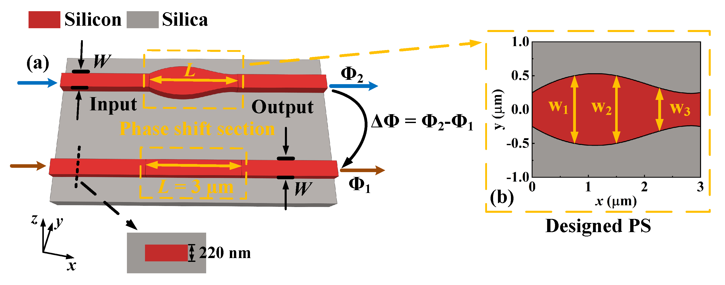
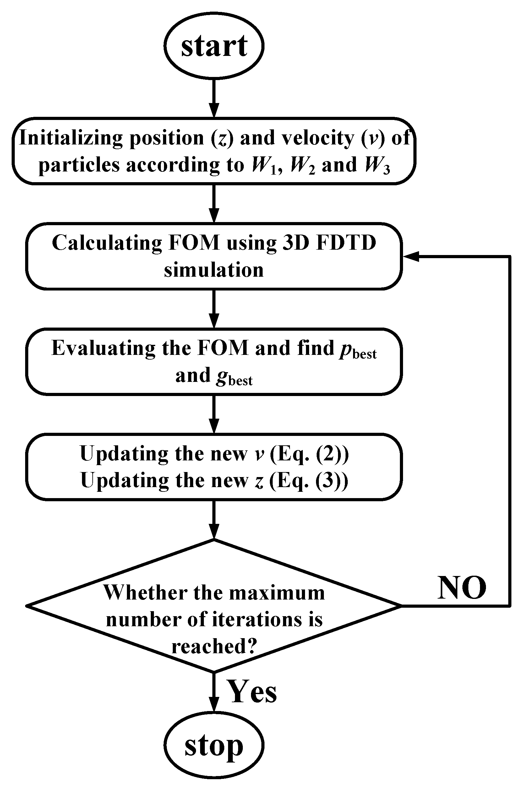
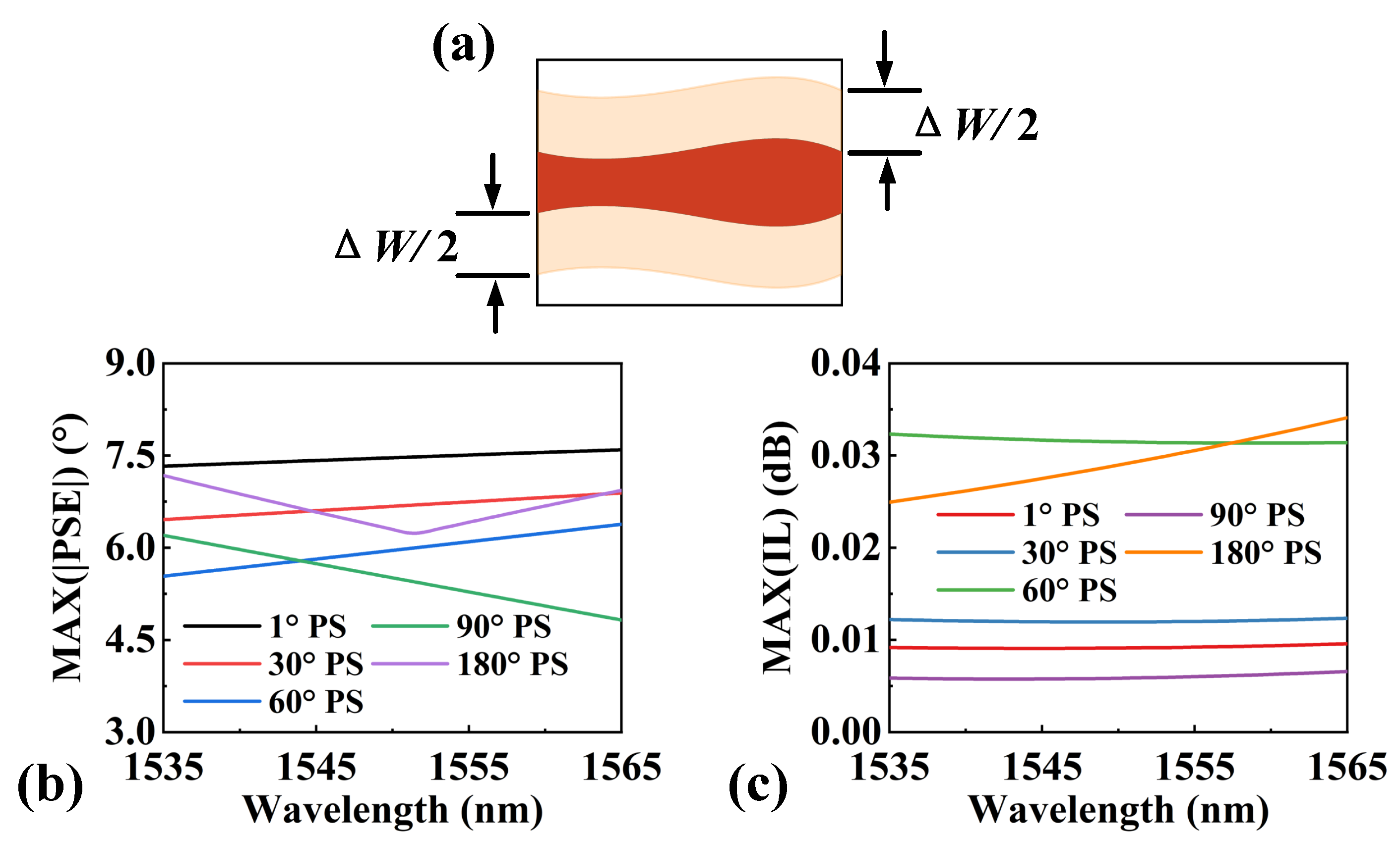
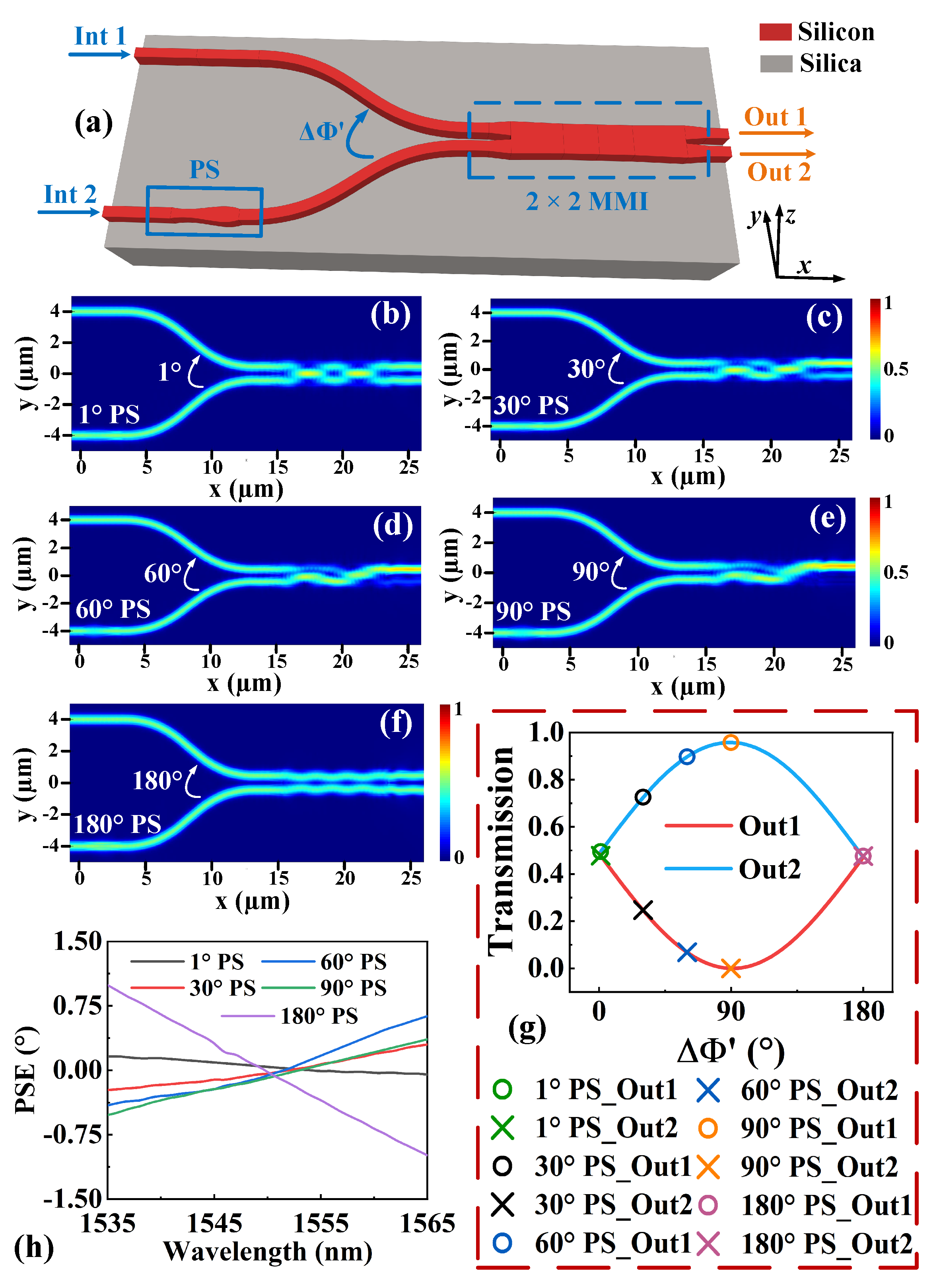
2. Design Principle
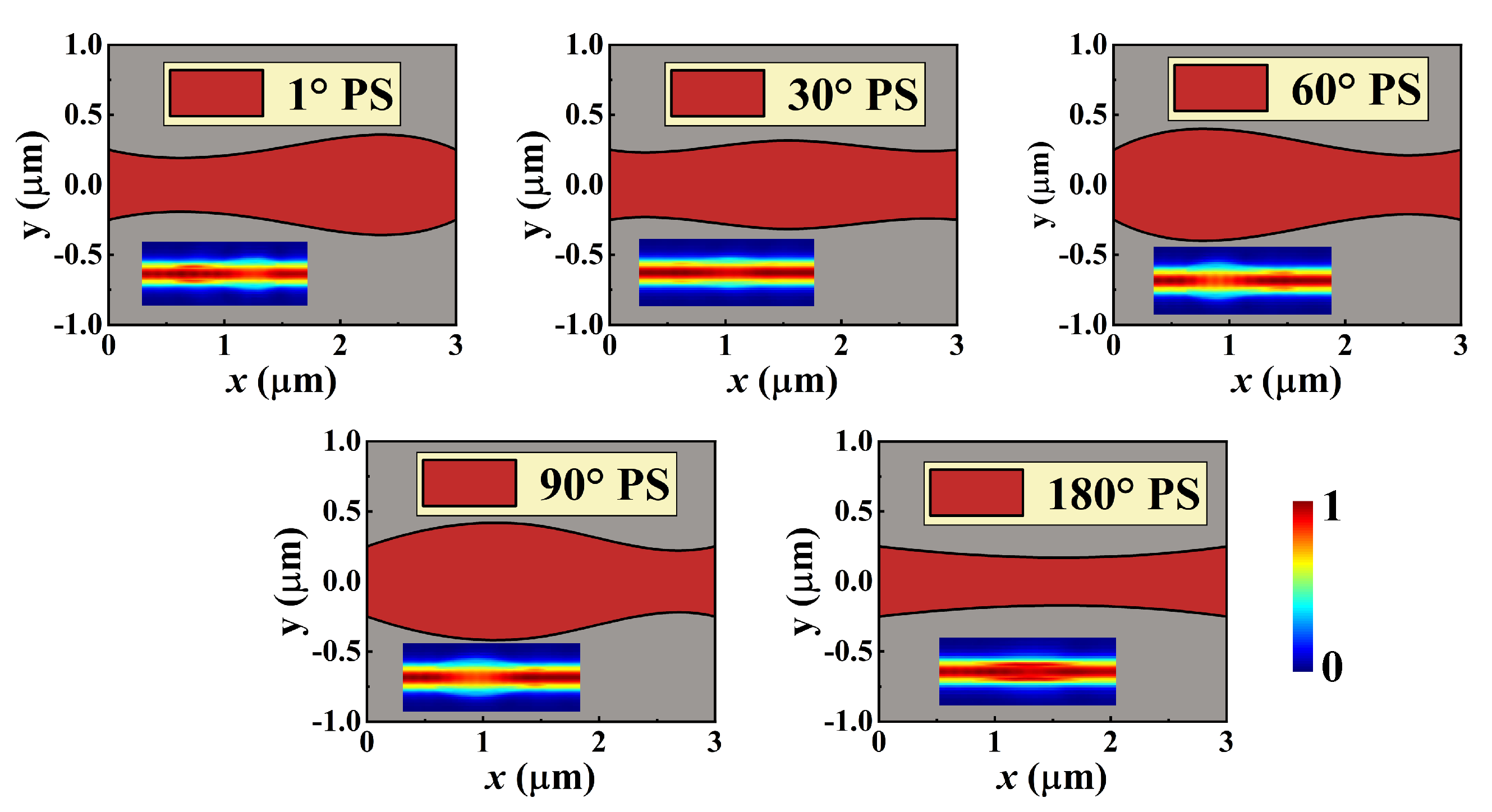
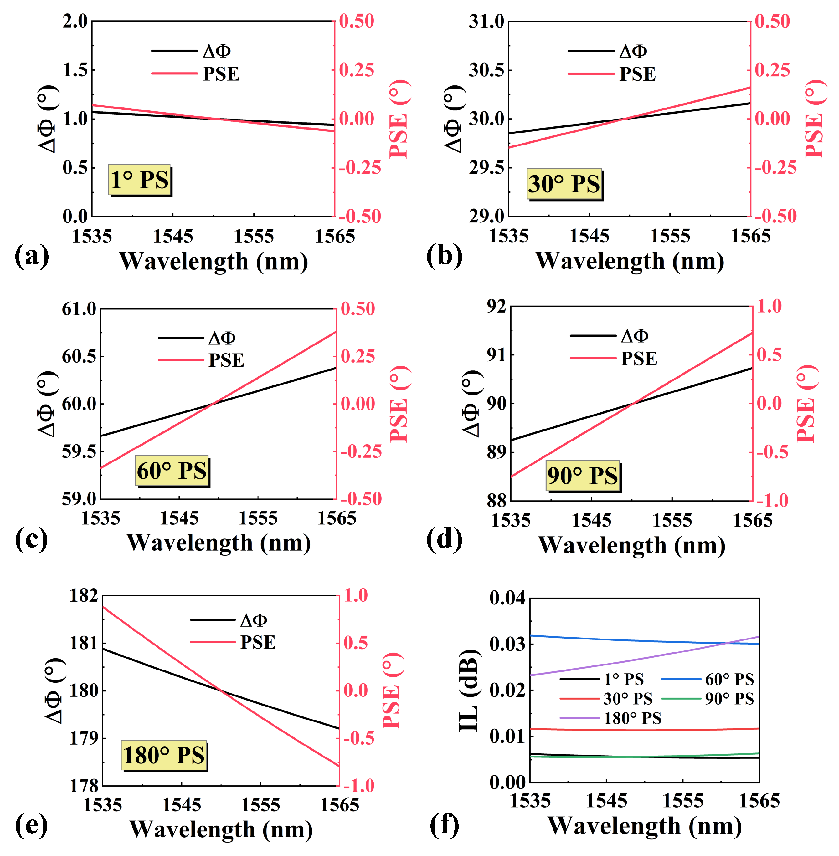
3. Results and Discussion
4. Conclusions
Author Contributions
Funding
Institutional Review Board Statement
Informed Consent Statement
Data Availability Statement
Acknowledgments
Conflicts of Interest
References
- Lin, Z.; Rusch, L.; Chen, Y.; Shi, W. Chip-scale, full-Stokes polarimeter. Opt. Express 2019, 27, 4867–4877. [Google Scholar] [CrossRef] [PubMed]
- Dong, P.; Chen, Y.K.; Duan, G.H.; Neilson, D.T. Silicon photonic devices and integrated circuits. Nanophotonics 2014, 3, 215–228. [Google Scholar] [CrossRef]
- Hochberg, M.; Baehr-Jones, T. Towards fabless silicon photonics. Nat. Photonics 2010, 4, 492–494. [Google Scholar] [CrossRef]
- Wu, W.J.; Zhao, W.S. A Quality Factor Enhanced Microwave Sensor Based on Modified Split-Ring Resonator for Microfluidic Applications. IEEE Sens. J. 2022, 22, 22582–22590. [Google Scholar] [CrossRef]
- Hillerkuss, D.; Winter, M.; Teschke, M.; Marculescu, A.; Li, J.; Sigurdsson, G.; Worms, K.; Ezra, S.B.; Narkiss, N.; Freude, W.; et al. Simple all-optical FFT scheme enabling Tbit/s real-time signal processing. Opt. Express 2010, 18, 9324–9340. [Google Scholar] [CrossRef]
- Doerr, C.R.; Winzer, P.J.; Chen, Y.K.; Chandrasekhar, S.; Rasras, M.S.; Chen, L.; Liow, T.Y.; Ang, K.W.; Lo, G.Q. Monolithic polarization and phase diversity coherent receiver in silicon. J. Light. Technol. 2009, 28, 520–525. [Google Scholar] [CrossRef]
- Knill, E.; Laflamme, R.; Milburn, G.J. A scheme for efficient quantum computation with linear optics. Nature 2001, 409, 46–52. [Google Scholar] [CrossRef] [PubMed]
- Harris, N.C.; Bunandar, D.; Pant, M.; Steinbrecher, G.R.; Mower, J.; Prabhu, M.; Baehr-Jones, T.; Hochberg, M.; Englund, D. Large-scale quantum photonic circuits in silicon. Nanophotonics 2016, 5, 456–468. [Google Scholar] [CrossRef]
- Zhao, W.; Liu, R.; Peng, Y.; Yi, X.; Chen, H.; Dai, D. High-performance silicon polarization switch based on a Mach–Zehnder interferometer integrated with polarization-dependent mode converters. Nanophotonics 2022, 11, 2293–2301. [Google Scholar] [CrossRef]
- Nikbakht, H.; Khoshmehr, M.T.; Van Someren, B.; Teichrib, D.; Hammer, M.; Förstner, J.; Akca, B.I. Asymmetric, non-uniform 3-dB directional coupler with 300-nm bandwidth and a small footprint. Opt. Lett. 2023, 48, 207–210. [Google Scholar] [CrossRef]
- Jeong, S.H.; Morito, K. Novel Optical 90° Hybrid Consisting of a Paired Interference Based 2 × 4 MMI Coupler, a Phase Shifter and a 2 × 2 MMI Coupler. J. Light. Technol. 2010, 28, 1323–1331. [Google Scholar] [CrossRef]
- Cherchi, M.; Ylinen, S.; Harjanne, M.; Kapulainen, M.; Vehmas, T.; Aalto, T. Unconstrained splitting ratios in compact double-MMI couplers. Opt. Express 2014, 22, 9245–9253. [Google Scholar] [CrossRef] [PubMed]
- Saida, T.; Himeno, A.; Okuno, M.; Sugita, A.; Okamoto, K. Silica-based 2 × 2 multimode interference coupler with arbitrary power splitting ratio. Electron. Lett. 1999, 35, 2031–2033. [Google Scholar] [CrossRef]
- Priti, R.B.; Bazargani, H.P.; Xiong, Y.; Liboiron-Ladouceur, O. Mode selecting switch using multimode interference for on-chip optical interconnects. Opt. Lett. 2017, 42, 4131–4134. [Google Scholar] [CrossRef] [PubMed]
- González-Andrade, D.; Olivares, I.; de Cabo, R.F.; Vilas, J.; Dias, A.; Velasco, A.V. Broadband three-mode converter and multiplexer based on cascaded symmetric Y-junctions and subwavelength engineered MMI and phase shifters. Opt. Laser Technol. 2023, 164, 109513. [Google Scholar] [CrossRef]
- Chaen, Y.; Tanabe, K.; Jiang, H.; Hamamoto, K. Low wavelength dependency design for MMI (multi-mode interference) mode converter. IEICE Electron. Express 2015, 12, 20150727. [Google Scholar] [CrossRef]
- Truong, C.D.; Nguyen, T.H.; Pham, Q.T.; Trinh, M.T.; Vu, K. Three-mode multiplexer and demultiplexer utilizing trident and multimode couplers. Opt. Commun. 2019, 435, 334–340. [Google Scholar] [CrossRef]
- Qiu, J.; Zhang, D.; Tian, Y.; Wu, J.; Li, Y.; Wang, Y. Performance analysis of a broadband second-order mode converter based on multimode interference coupler and phase shifter. IEEE Photonics J. 2015, 7, 1–8. [Google Scholar]
- González-Andrade, D.; Wangüemert-Pérez, J.G.; Velasco, A.V.; Ortega-Monux, A.; Herrero-Bermello, A.; Molina-Fernandez, I.; Halir, R.; Cheben, P. Ultra-broadband mode converter and multiplexer based on sub-wavelength structures. IEEE Photonics J. 2018, 10, 1–10. [Google Scholar] [CrossRef]
- Morrissey, P.; Peters, F. Multimode interference couplers as compact and robust static optical phase shifters. Opt. Commun. 2015, 345, 1–5. [Google Scholar] [CrossRef]
- González-Andrade, D.; Luque-González, J.M.; Wangüemert-Pérez, J.G.; Ortega-Moñux, A.; Cheben, P.; Molina-Fernández, Í.; Velasco, A.V. Ultra-broadband nanophotonic phase shifter based on subwavelength metamaterial waveguides. Photonics Res. 2020, 8, 359–367. [Google Scholar] [CrossRef]
- Molesky, S.; Lin, Z.; Piggott, A.Y.; Jin, W.; Vucković, J.; Rodriguez, A.W. Inverse design in nanophotonics. Nat. Photonics 2018, 12, 659–670. [Google Scholar] [CrossRef]
- Zhang, G.; Xu, D.X.; Grinberg, Y.; Liboiron-Ladouceur, O. Experimental demonstration of robust nanophotonic devices optimized by topological inverse design with energy constraint. Photonics Res. 2022, 10, 1787–1802. [Google Scholar] [CrossRef]
- Kim, J.; Kim, J.Y.; Yoon, J.; Yoon, H.; Park, H.H.; Kurt, H. Experimental demonstration of inverse-designed silicon integrated photonic power splitters. Nanophotonics 2022, 11, 4581–4590. [Google Scholar] [CrossRef]
- Goudarzi, K.; Lee, M. Inverse design of a binary waveguide crossing by the particle swarm optimization algorithm. Results Phys. 2022, 34, 105268. [Google Scholar] [CrossRef]
- Chen, W.; Li, H.; Zhang, B.; Wang, P.; Dai, S.; Liu, Y.; Li, J.; Li, Y.; Fu, Q.; Dai, T.; et al. Silicon mode (de) multiplexer based on cascaded particle-swarm-optimized counter-tapered couplers. IEEE Photonics J. 2020, 13, 1–10. [Google Scholar] [CrossRef]
- Robinson, J.; Rahmat-Samii, Y. Particle swarm optimization in electromagnetics. IEEE Trans. Antennas Propag. 2004, 52, 397–407. [Google Scholar] [CrossRef]
- Guan, H.; Ma, Y.; Shi, R.; Zhu, X.; Younce, R.; Chen, Y.; Roman, J.; Ophir, N.; Liu, Y.; Ding, R.; et al. Compact and low loss 90° optical hybrid on a silicon-on-insulator platform. Opt. Express 2017, 25, 28957–28968. [Google Scholar] [CrossRef]


| Parameters | 1 PS | 30 PS | 60 PS | 90 PS | 180 PS |
|---|---|---|---|---|---|
| (µm) | 0.389 | 0.513 | 0.799 | 0.8 | 0.386 |
| (µm) | 0.534 | 0.632 | 0.659 | 0.789 | 0.342 |
| (µm) | 0.712 | 0.538 | 0.45 | 0.522 | 0.377 |
Disclaimer/Publisher’s Note: The statements, opinions and data contained in all publications are solely those of the individual author(s) and contributor(s) and not of MDPI and/or the editor(s). MDPI and/or the editor(s) disclaim responsibility for any injury to people or property resulting from any ideas, methods, instructions or products referred to in the content. |
© 2023 by the authors. Licensee MDPI, Basel, Switzerland. This article is an open access article distributed under the terms and conditions of the Creative Commons Attribution (CC BY) license (https://creativecommons.org/licenses/by/4.0/).
Share and Cite
Liao, J.; Tian, Y.; Kang, Z.; Zhang, X. Inverse Design of Ultra-Compact and Low-Loss Optical Phase Shifters. Photonics 2023, 10, 1030. https://doi.org/10.3390/photonics10091030
Liao J, Tian Y, Kang Z, Zhang X. Inverse Design of Ultra-Compact and Low-Loss Optical Phase Shifters. Photonics. 2023; 10(9):1030. https://doi.org/10.3390/photonics10091030
Chicago/Turabian StyleLiao, Junpeng, Ye Tian, Zhe Kang, and Xiaowei Zhang. 2023. "Inverse Design of Ultra-Compact and Low-Loss Optical Phase Shifters" Photonics 10, no. 9: 1030. https://doi.org/10.3390/photonics10091030