1. Introduction
Extending the optical communication window to the emerging 2 μm waveband holds several unique advantages, like wide gain bandwidth of the available thulium doped fiber [
1] and the low fiber attenuation of the hollow-core photonic bandgap fiber [
2]. It also shows great potential for free-space optical communications due to the advantages of eye safety [
3] and atmosphere low absorption [
4]. Driven by these prospects, a few laboratory demonstrations of the high-speed data transmission have been reported using discrete, packaged components [
5,
6,
7]. The state-of-the-art narrow-line width laser [
8], high-speed photodetectors [
9], and modulator [
10] are available on III–V materials or the lithium niobate platform. As a proven integration platform, the silicon photonic components at the 2 μm waveband have gained great interest. Efforts have been devoted to developing the modulators [
11,
12,
13], filters [
14], multiplexers [
15], splitters [
16,
17], resonators [
18], couplers [
19], and so forth.
Grating couplers are fundamental elements that enable bidirectional light transmission between the waveguides and optical fibers. Extensive efforts have been devoted to developing high-coupling-efficiency grating couplers for C-band [
20,
21,
22,
23]. Coupling efficiency is typically defined as the ratio of the optical power transmitted from the input waveguide to the fiber and then to the input optical power. Two main approaches have been explored to optimize the coupling efficiency of the grating coupler. The first approach is to optimize the directionality of the grating coupler, which is generally defined as the ratio of the optical power diffracted upward by the grating to the optical power diffracted by the grating. Previous research has demonstrated that structures such as bottom reflectors [
24] can be utilized to improve the directionality. The second approach is to adjust the diffraction mode field to match the Gaussian mode field of the fiber. A uniform grating coupler has a diffraction mode field that exponentially decays along the propagation direction, making it difficult to match with the Gaussian diffraction mode spot of fiber transmission, thereby resulting in a reduced coupling efficiency. To overcome this mode-mismatch problem and improve the coupling efficiency, one can arrange the diffraction intensity of each period of the grating or design a non-uniform grating coupler using inverse design [
25] to obtain a nearly satisfactory Gaussian beam output. It has been shown that a 220 nm thick silicon-on-insulator with a shallow etching depth allows for reasonably good performance for coupling the C-band waves. However, achieving efficient coupling in the extended 2 μm waveband remains challenging due to the considerable difference in wavelength scale, which results in the deterioration of directionality.
In the 2 μm wavelength range, several grating coupler designs based on the 220 nm silicon-on-insulator (SOI) waveguides have been proposed [
19,
26]. Most of these designs focus on optimizing the grating period and fill factor to improve the matching between the diffracted mode field of the grating coupler and the mode field of the optical fiber, or on using processes such as hollowing out the buried oxide layer substrates that are incompatible with CMOS technology to improve directionality. However, these designs are difficult to significantly improve the coupling efficiency, and the coupling efficiency is significantly constrained by the top silicon thickness. While several efficient coupling devices were reported by adopting a top silicon layer with a 340 nm thickness, it is not an optimal option for other devices such as modulators. Moreover, as a large number of multi-band devices [
27] or large bandwidth devices [
14] have been proposed, integrating devices for both the 1.55 µm and 2 µm wavebands on the same chip is a promising solution for expanding the bandwidth of the silicon-based integrated chips. Efficient grating couplers with a top silicon layer thickness of 340 nm are difficult to integrate with these large bandwidth dual-band devices designed based on a top silicon layer thickness of 220 nm on the same chip. Therefore, the low coupling efficiency of the grating couplers based on the SOI waveguides with a 220 nm thickness in the 2 μm waveband limits the practical application prospects of multi-band devices and large bandwidth devices.
In this paper, an efficient grating coupler based on the raised polysilicon on a 220 nm thick SOI is proposed and designed at a central wavelength of 2002 nm. The polysilicon atop the silicon increases the effective refractive index difference between the tooth and the groove, allowing for improved directionality and coupling strength. A dual-layer grating was formed and optimized separately which offers a much larger degree of freedom for grating design. The arrangement of the dual-layer grating was realized via inverse design. For the fiber tilted at an angle of 10°, the grating coupler’s simulated coupling efficiency reaches 80.3% (−0.95 dB) at a wavelength of 2002 nm. The 1 dB bandwidth is 66 nm. The grating coupler has a minimum feature size of 220 nm which can be easily fabricated via state-of-the-art processes. It offers a simple solution for the efficient grating coupler of a 2 μm band which shares the same substrate and process with the mature devices at 1.55 μm wavelengths.
2. Device and Result
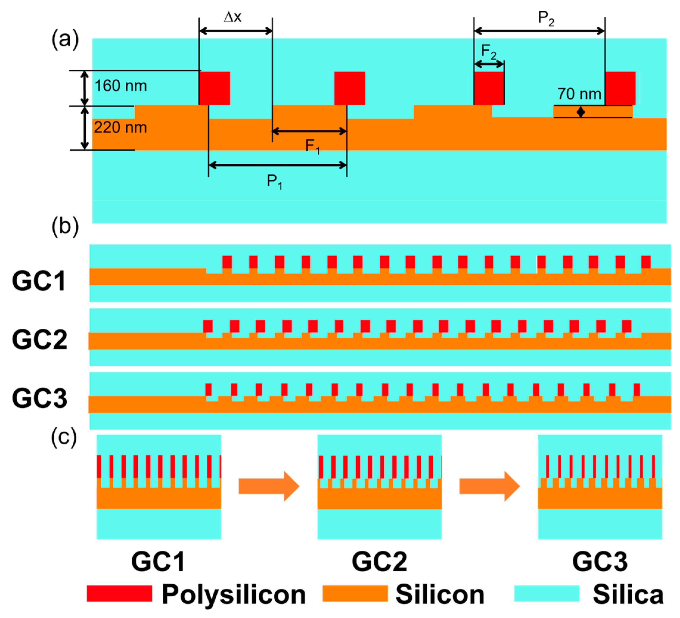
The grating coupler is designed on the standard SOI platform with a polysilicon overlay, which is available from commercial silicon photonic foundries. The thickness of the top silicon layer is 220 nm, and the thickness of the buried oxide layer is 2 μm. The raised polysilicon layer on top of the silicon has a thickness of 160 nm. As shown by the side-view schematic diagram of the grating coupler in
Figure 1a, the polysilicon layer is fully etched with a 160 nm depth while the top silicon is shallowly etched with a 70 nm depth. The grating couplers proposed in this work are covered by the top oxide cladding. First, a single-layer raised polysilicon grating coupler (GC1) is designed by varying the grating periods and filling factors. Here, we define the filling factor as the ratio of the grating tooth length to the grating period. Then, a double-layer grating coupler (GC2) is designed by introducing a small displacement between the polysilicon grating teeth and the silicon grating teeth. Finding an optimal dislocation allows us to further improve the directionality. For GC2, the filling factor and the period are consistent for the polysilicon and silicon layer. It would be beneficial if the parameters of the two layers could be optimized separately. As shown by GC3 in
Figure 1b, up to five parameters, including the grating displacement (Δx), filling factors (F1 and F2), and the periods (P1 and P2) of the two layers, are jointly optimized via the particle swarm optimization (PSO) algorithm. The figure of merit is defined as the coupling efficiency. Such a huge design freedom of the proposed structure allows for a significant improvement of the efficiency for a 2 μm spectral range. The complete three-step optimization process of the grating coupler is shown in
Figure 1c.
For a 2 μm waveband, the 220 nm top silicon has very limited mode confinement which induces unwanted wave radiations. Increasing the waveguide thickness is an effective way to improve the confinement, which has been well demonstrated for C-band grating couplers. Intuitively, an overlay of polysilicon is highly desired, especially for longer wavelengths, which is expected to mitigate the light dissipation. The performance of all proposed devices was evaluated using 2D finite-difference time-domain (2D FDTD) simulations with a simulation region size of 28 μm × 8 μm, a simulation accuracy of 3, and perfectly matched layer (PML) boundary conditions. We designed a grating coupler for transmitting the TE mode and simulated it using a SMF28 fiber, while also using a Gaussian mode field. The refractive indices of the polycrystalline silicon and the single crystal silicon are extremely close in the 2 μm waveband (n
Si = n
Polysilicon = 3.47) [
28]. In addition, the refractive index of silicon dioxide is set at 1.4379. The specific refractive index parameters are shown in
Table 1.
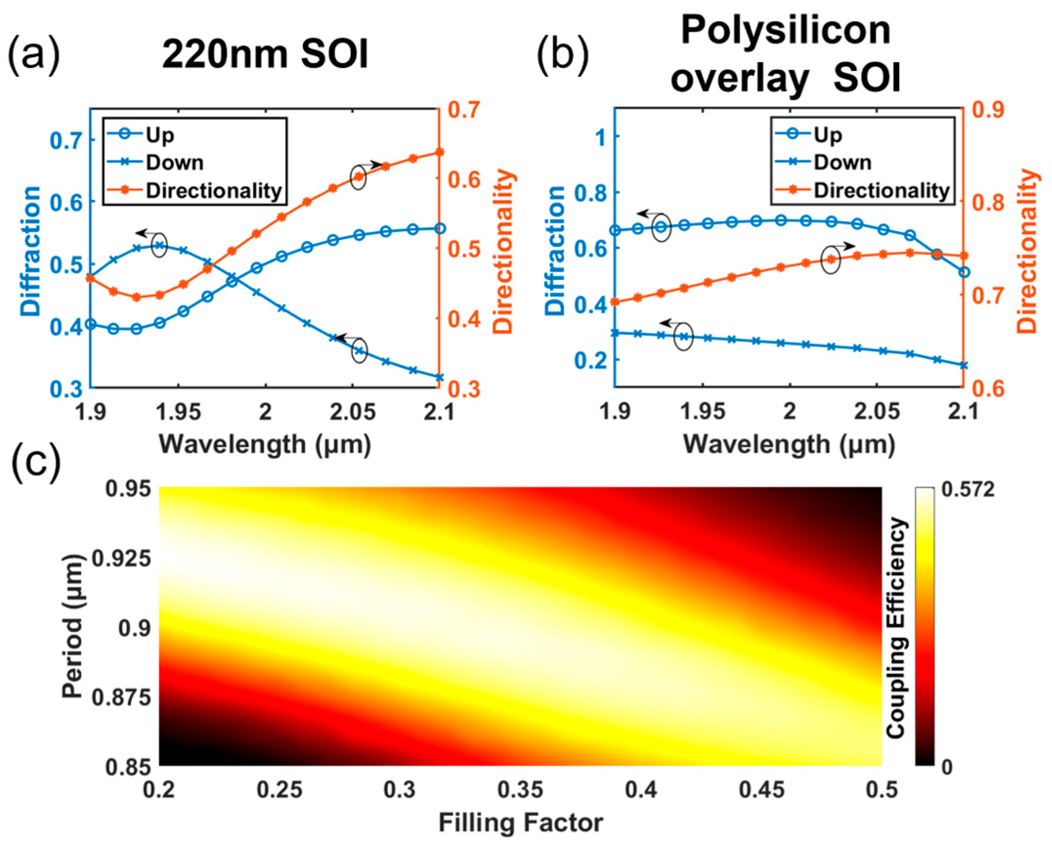
Firstly, we design a uniform grating (GC1) based on the raised polysilicon layer without dislocation between the two layers. In practical applications, an optical fiber is placed at the top of a grating coupler to receive the energy transmitted by the coupler. Therefore, to achieve higher coupling efficiency, the grating coupler needs to diffract more light upwards rather than downwards towards the substrate. To better analyze the directionality of the grating coupler, the Up Diffraction Percentage is defined as the ratio of the optical power diffracted upwards to the input optical power, while the Down Diffraction Percentage is defined as the ratio of the optical power diffracted downwards to the input optical power. As suggested by the simulation results in
Figure 2a, the directionality of the 2 μm band grating coupler based on the 220 nm thick SOI substrate is normally constrained to 63.7% under the fully etching condition, which is limited by the weak mode confinement. In other words, the small difference in the effective refractive index between the tooth and groove results is weak coupling strength. Even for a fully etched grating, the insufficient grating coupling strength has to be compensated by extending the coupling length which induces dissipation of a considerable portion of light. However, as a symmetrical structure grating, the directionality of the fully etched grating coupler relies on the interference between the reflected and transmitted light, where constructive interference occurs upward and destructive interference occurs downward, achieving high directionality. However, interference is closely related to the wavelength, so high directionality can only be achieved within a narrow wavelength range, and the directionality will fluctuate with the wavelength, which is consistent with the results shown in
Figure 2a. This wavelength-dependent directionality significantly limits the fully etched grating coupler’s bandwidth performance. In contrast, as shown by the results in
Figure 2b, the directionality of the grating coupler with polysilicon atop the SOI platform approaches 75%. A flat response can be achieved over a wide spectral band from 1900 nm to 2100 nm. Unlike constructive interference, adding a polysilicon overlay is effective for enhancing mode confinement or improving the effective refractive index difference throughout the entire 2 µm wavelength band. In other words, the wavelength-insensitive nature of the polysilicon overlay makes it an effective means of improving the directionality of the grating cou-pler, thereby significantly improving its performance over the entire 2 µm wavelength band and potentially enabling the design of broadband grating couplers on this plat-form.
Since the grating coupler needs to satisfy the grating equation (Equation (1)), the approximate values of the structural parameters, such as the filling factor and the period of the grating coupler that determines the diffraction angle, can be obtained via the method based on the grating equation below.
where
λ represents the center wavelength of the grating coupler, which is 2 µm in this design. n
eff represents the effective refractive index of the grating coupler which is determined via the fill factor. n
SiO2 represents the refractive index of the silica in the wavelength of 2 μm.
θ represents the diffraction angle of the grating coupler, which is 10° in this design. Λ represents the period of the grating coupler.
From the grating equation, it can be seen that when the diffraction angle and the central wavelength are fixed, the period of the grating coupler and the filling factor correspond to each other. In order to obtain a high-efficiency single-layer grating coupler (GC1), a parameter scan of the filling factor and period was performed. As shown in
Figure 2c, an optimal coupling efficiency of 57.2% (−2.42 dB) can be achieved by choosing the filling factor of 0.20 and the period of 925 nm. It reveals the efficiency improvement by simply adopting a raised silicon overlay.
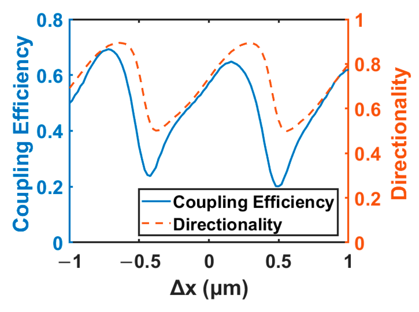
Though the single-layer raised polysilicon grating coupler (GC1) increases the directionality compared with the bare silicon grating with a 220 nm thickness, it is not the optimal directionality. Here, an offset dual-layer grating coupler is further proposed as GC2. By introducing a small displacement defined as Δx between the polysilicon and silicon grating teeth, the offset dual-layer grating coupler (GC2) is based on the single-layer raised polysilicon grating coupler (GC1), with no change in etching depth and a fixed grating coupler filling factor and period. By adjusting the displacement, we have constructed a structure similar to lazed grating or shallow-etched grating, which can further improve the directionality.
Figure 3 shows the simulated directionality and the corresponding coupling efficiency under different values of Δx. It can be seen that the periodic feature of the curve implies the interference between the upward diffraction and bottom reflection beams. For proper dislocation of Δx, coherent constructive interference can be achieved to maximize the directionality. It is worth noting that the initial structure with a 160 nm thick polysilicon overlay and a 70 nm shallow etching on the silicon is not the optimal structure. This is why we need to detune the displacement of the polysilicon grating teeth to further improve the directionality. By choosing a proper displacement between the two grating layers of Δx = −720 nm, an optimal directionality of 89% can be achieved. In the meantime, the corresponding coupling efficiency of 68.3% (−1.66 dB) can be expected. Such a high efficiency is challenging for the bare silicon grating coupler with either a 220 nm or 340 nm thickness since the grating displacement is only achievable via a dual-layer structure.
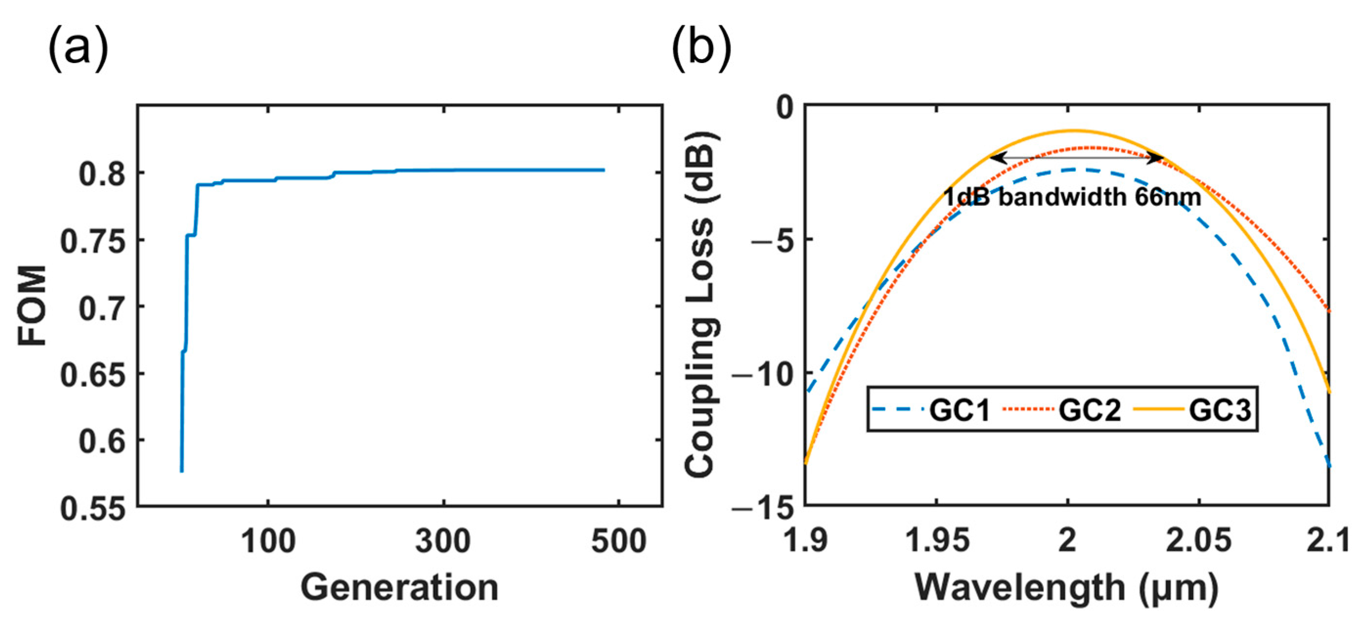
Based on the results and analysis from the previous two steps of the design, we find that the grating displacement, period, and filling factor of the two grating layers have a significant impact on the coupling efficiency. Intuitively, the performance can be potentially improved further if the grating filling factor and the period can be designed separately for both silicon layers, which results in a completely dual-layer grating coupler (GC3). Coincidentally, if we optimize the five structural parameters in a coordinated manner, the diffraction intensity of each period of the double-layer grating is different, achieving the diffraction performance of a non-uniform grating coupler. That is, precise arrangement of the grating period and fill factor for the non-uniform grating coupler can be achieved by optimizing the coordination of only five parameters. As a result, up to five structural parameters have to be optimized jointly. Here, the numerical simulations are combined with the particle swarm optimization (PSO) algorithm to iteratively optimize the periods, the filling factors, and the displacement offset of the two grating layers. The range in variation in the period of the upper and lower grating layers is set from 0.85 μm to 0.95 μm, while the fill factor of the upper grating is set from 0.2 to 0.5, and the fill factor of the lower grating is set from 0.2 to 0.8. The range of Δx is set from −1 μm to 0 μm. The figure of merit (FOM) can be simply defined as the coupling efficiency for the optimization target. As shown in
Figure 4a, the efficiency goes up quickly with only tens of iterations by using a normal desktop with a 12-core CPU (Intel Core i7-12700K). The FOM climbs up slowly when it approaches 80%, and it tends to converge after 340 iterations, as all the above simulation processes take only 1 day to complete. Here, a benchmark coupling efficiency of −0.95 dB (80.3%) is achieved at a center wavelength of 2002 nm. The corresponding device structure parameters of GC3 are summarized in
Table 2. The structure is fabrication-friendly with a minimum feature size of 220 nm. The device is fully compatible with the design rules of several standard silicon photonic foundries. For comparison, the coupling efficiencies of the single-layer raised polysilicon grating coupler (GC1), offset dual-layer grating coupler (GC2), and real dual-layer grating coupler (GC3) are plotted in
Figure 4b. The proposed PSO-optimized GC3 not only achieves a low coupling loss of −0.95 dB but is also capable of broadband operation with a 1 dB bandwidth of 66 nm. As a credit to the much larger design freedom of GC3 and the powerful optimization capability of the PSO algorithm, less than a 1 dB coupling loss can be achieved by matching the mode field of the diffraction beam and the optical fiber.
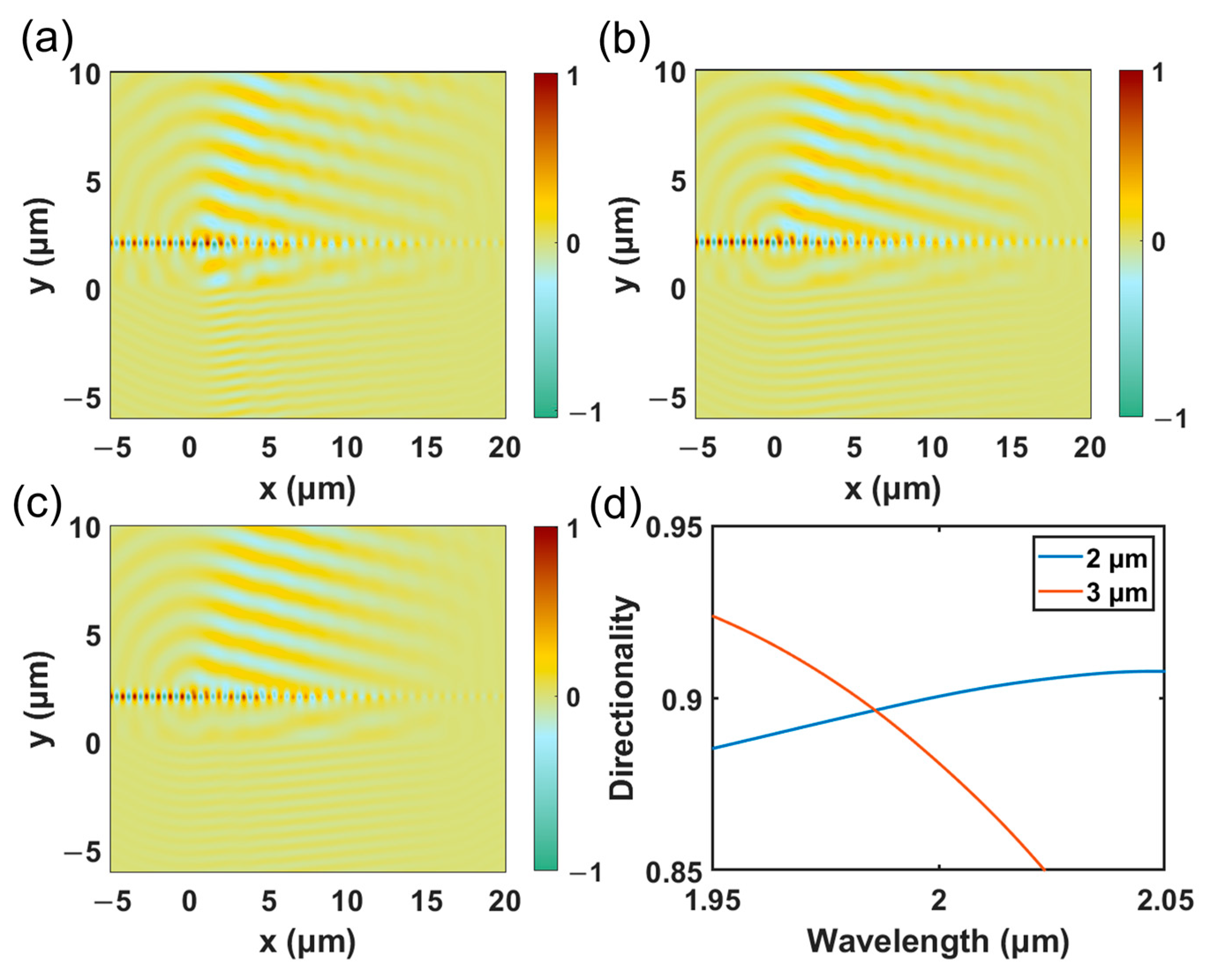
To better study the diffraction behavior of the grating coupler, the simulation area was expanded in the y-direction from −6 μm to 10 μm, and the z-component of the electric field in the grating coupler was studied.
Figure 5a–c shows the z-components of the electric field distribution of GC1, GC2, and GC3, respectively. From
Figure 5a, it can be seen that in the uniform single-layer grating (GC1), the light undergoes strong diffraction at the front end of the grating, resulting in an exponential decay of the diffraction field power which does not match the Gaussian mode profile of the single-mode fibers. A similar problem also appears in the mode distribution of GC2, which is actually a double-layer uniform grating. Due to the misalignment between the gratings, the effective refractive index difference at the front end of the grating is reduced, resulting in lower diffraction intensity. Therefore, it can be observed from
Figure 5b that the normalized z-component of the electric field distribution does not exhibit a very obvious maximum diffraction intensity at the front end of the grating. For the PSO-optimized GC3, the size of the grating at the front end is smaller and the diffraction intensity is lower, resulting in a diffraction beam profile that matches well with the Gaussian fiber mode, consistent with a higher coupling efficiency. It is very interesting to note that the polysilicon and silicon grating layer can be designed with a completely non-uniform structure which might be able to further improve the coupling performance. However, the computation cost will be significantly higher than the GC3. In addition, from a directional perspective, due to the interference behavior between the interface reflected light and transmitted light, a buried layer with a thickness of 2 μm is not the optimal choice in the 2 μm wavelength range, which also affects the directionality of GC1. As for GC2 and GC3, which are double-layer grating couplers, their optical path length differs from that of ordinary single-layer grating couplers. In the 2 μm waveband, the directionality of GC3 with respect to the buried layer thickness is shown in
Figure 5d, where there is little difference between a buried layer thickness of 2 μm and 3 μm. Furthermore, compared to a thickness of 3 μm, selecting a thickness of 2 μm for the buried layer can maintain higher directionality over a wider wavelength range, giving GC3 a larger bandwidth.
In
Table 3, several recent works on 2 μm waveband grating couplers are summarized and compared. Most of these grating couplers are implemented on the SOI with a thickness of 220 nm or 340 nm, and their coupling efficiency is limited. Various approaches such as non-uniform period grating couplers, hollowing out the buried oxide layer, and shallowly etched grating couplers have been attempted to improve the performance of the grating couplers in the 2 µm wavelength band. However, these approaches have not been able to address the problem of low directionality in the 2 µm wavelength band on the 220 nm SOI platform, making it difficult to achieve a satisfactory optimized coupling efficiency for the grating couplers and limiting the practical application prospects for many broadband devices. The structure proposed in this work demonstrates a record high efficiency with a simple structure which is fully compatible with the standard foundry process. The designed grating can be easily fabricated by adding a step of polysilicon deposition and an etching process [
29]. In addition, the bandwidth is also much larger than the other works, which is a credit to the large directionality improvement.
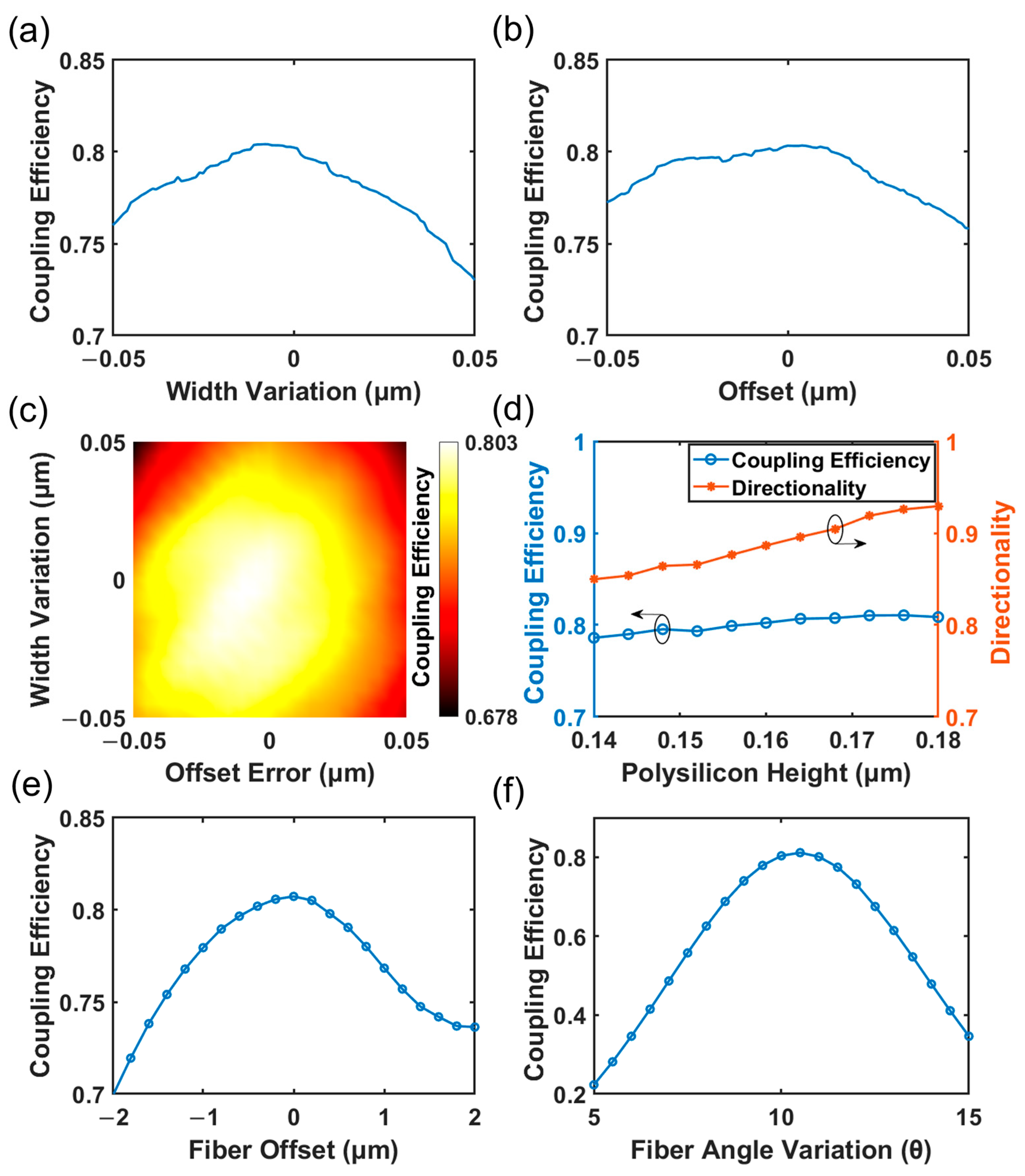
In the 2 μm band, the grating equation determines the nanoscale feature sizes of the grating couplers in the silicon-based photonics. However, due to the nature of nanoscale manufacturing, it is difficult to avoid manufacturing variations. Therefore, the tolerance of grating couplers to manufacturing variations is a critical factor in determining the coupling efficiency of these devices. In this study, we analyzed the effect of manufacturing differences, such as variations in the thickness of polysilicon deposition, the width variation in the grating grooves, and the etching offset between the polysilicon layer gratings and the silicon layer gratings on the performance of the designed grating couplers via numerical simulations.
As shown in
Figure 6a,b, the impact of offset and width variation on the coupling efficiency of the optimized grating couplers was minimal. Even when the offset was ±50 nm, the coupling efficiency remained above 75%. Similarly, when the width variation was ±50 nm, the coupling efficiency was above 70%.
Figure 6c indicates that the simultaneous occurrence of these two variations within a ±50 nm range had an acceptable impact on the coupling efficiency, which are the largest manufacturing variations in multi-project wafer (MPW) foundries.
Figure 6d illustrates the effect of the polysilicon deposition thickness on the performance of the grating couplers. It can be observed that if the polysilicon deposition thickness is smaller than 160 nm, the coupling efficiency will decrease to some extent due to the decrease in directionality. However, when the thickness reaches 160 nm, changes in the thickness no longer affect performance and may even further enhance the coupling efficiency, which can be attributed to the change in directionality caused by the thickness variation. These findings indicate that the grating couplers exhibit a high tolerance to the manufacturing variations, demonstrating significant potential for practical applications. Similarly, the position and angle of the fiber can also affect the coupling efficiency of the optical grating coupler, so we simulated the impact of fiber placement and tilt angle on the GC3. As shown in
Figure 6e, the GC3 is not sensitive to the position of the fiber, and a coupling efficiency higher than 70% can be achieved within a placement error of ±2 μm. However, the GC3 is relatively sensitive to the tilt angle of the fiber, as indicated in
Figure 6f. Nonetheless, an investigation into the fiber tilt angle reveals that setting the coupling angle at 10.5° yields a higher coupling efficiency, achieving a value of 0.92 dB (81%).


