Article

Reduction in the Number of Current Sensors of a Semi-Bridgeless PFC Rectifier Based on GaNFET Characteristics

Department of Electrical Engineering, National Taipei University of Technology, 1, Sec. 3, Zhongxiao E. Rd., Taipei 10608, Taiwan
*
Author to whom correspondence should be addressed.
Processes 2023, 11(12), 3259; https://doi.org/10.3390/pr11123259
Submission received: 19 October 2023 / Revised: 10 November 2023 / Accepted: 18 November 2023 / Published: 21 November 2023

Abstract

:
The semi-bridgeless power factor correction (PFC) rectifier is widely used due to its high power factor, high efficiency, and low electromagnetic interference. However, in this rectifier, the inductor current will flow through the body diode of the metal–oxide–semiconductor field-effect transistor (MOSFET) when the MOSFET does not work, causing a problem in detecting the inductor current. Consequently, the current transformers are generally used as current sensors. This means that using many current sensors will make the cost and the peripheral detection circuit complicated. In this paper, our new method is to use a gallium nitride field-effect transistor (GaNFET) to replace the metal–oxide–semiconductor field-effect transistor (MOSFET) in the main switch selection. The reverse-biased conduction voltage of the third quadrant of the GaNFET is higher than the forward-biased conduction voltage of the diode, which solves the problem in detecting the inductor current, reduces the number of current sensors, and simplifies the corresponding peripheral circuits and components. Eventually, via mathematical deduction and hardware implementation, a semi-bridgeless PFC prototype with a GaNFET was built to verify the effectiveness of the proposed structure.

1. Introduction

With the rapid development of information and technology, there are more and more electronic devices for industry, business, and even the home. Cell phones, personal computers, home appliances, and other electronic products are also undergoing rapid and continuous innovation. The power supply used by these electronic devices is DC voltage, but most of the current power systems provide AC power, so it is necessary to convert the AC power to DC voltage. The simplest way to do this is to use a bridge rectifier consisting of diodes to rectify the AC power supply, which is then filtered by a bulk capacitor to obtain the DC voltage [1,2,3]. However, the input current is a steep pulse due to the charging current in the capacitor. Consequently, the current harmonics are large, causing serious harmonic pollution to the power grid and resulting in interference with the normal operation of other electrical equipment connected to the power grid. Accordingly, it is necessary to take measures to limit the current harmonics generated by these electronic devices, and the International Electrotechnical Commission (IEC) has issued the IEC 61000-3-2 current harmonic standard, which formally regulates the current harmonics created by electronic devices in detail [4,5,6].
In order to comply with the limit values of the IEC 61000-3-2 current harmonic standard, the power factor correction (PFC) must be added to make the input current sinusoidal and in phase with the input voltage of the power supply to increase the effective power so that the harmonic components of the input current will be reduced. The power factor correction (PFC) rectifier can be categorized as passive or active [7]. The traditional active PFC rectifier has a bridge rectifier at the front end, which accounts for a significant portion of the power loss. Therefore, if the power loss of this bridge rectifier can be reduced, the overall efficiency will be improved.
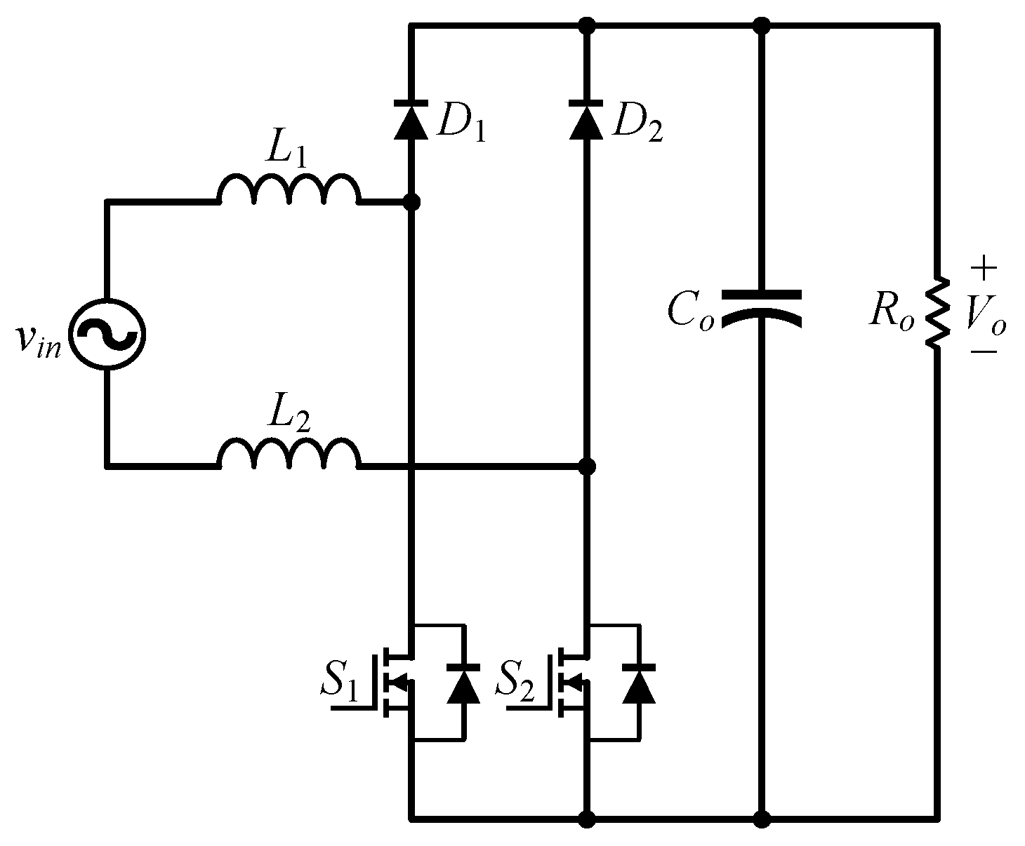
Figure 1 shows the basic, widely used semi-bridgeless PFC rectifier [8,9,10], which improves the overall efficiency by replacing two diodes with two MOSFETs. The disadvantages of this structure are the inconvenience of detecting the input voltage and inductor current [11,12,13] and the problem of electromagnetic interference (EMI) between the input and output due to the common-mode noise generated by high-switching power semiconductor devices [14,15].
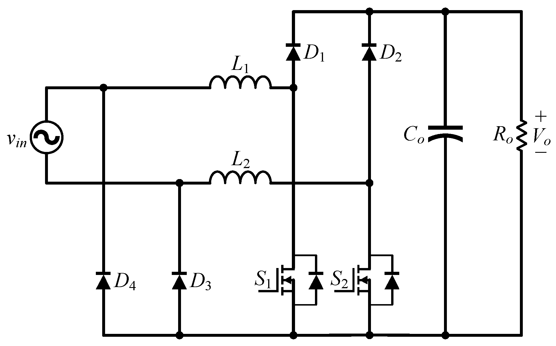
Figure 2 shows the semi-bridgeless PFC rectifier [16,17,18,19,20,21,22,23,24,25,26,27,28,29], which is a modified version of the basic, widely used semi-bridgeless PFC rectifier. In this modified circuit, two additional slow diodes, D3 and D4, are connected between the negative and positive terminals of the input AC voltage vin and the negative terminal of the output capacitor Co, respectively, to reduce the common-mode noise and, hence, to solve the EMI problem [14,15]. Furthermore, due to these two diodes, the input voltage can be detected directly by the resistive voltage divider. However, the inductor current will flow through the body diode of the inactivated MOSFET main switch, leading to an error in detecting the inductor current, causing a more complex current-detecting circuit to be required.
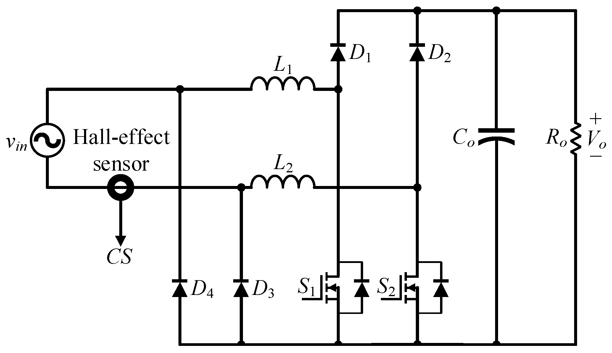
In order to solve the problem of detecting the inductor current, [30] suggests three methods to obtain the detected inductor current signal CS: Hall sensor detection, differential amplifier detection, and current transformer detection. These three methods are described below:
(1) Hall effect sensor detection
This method only requires the Hall effect sensor to be placed directly on the input to detect the inductor current, as shown in Figure 3. This method is simple, and the detected value is accurate and reliable, but the Hall sensor is more expensive.
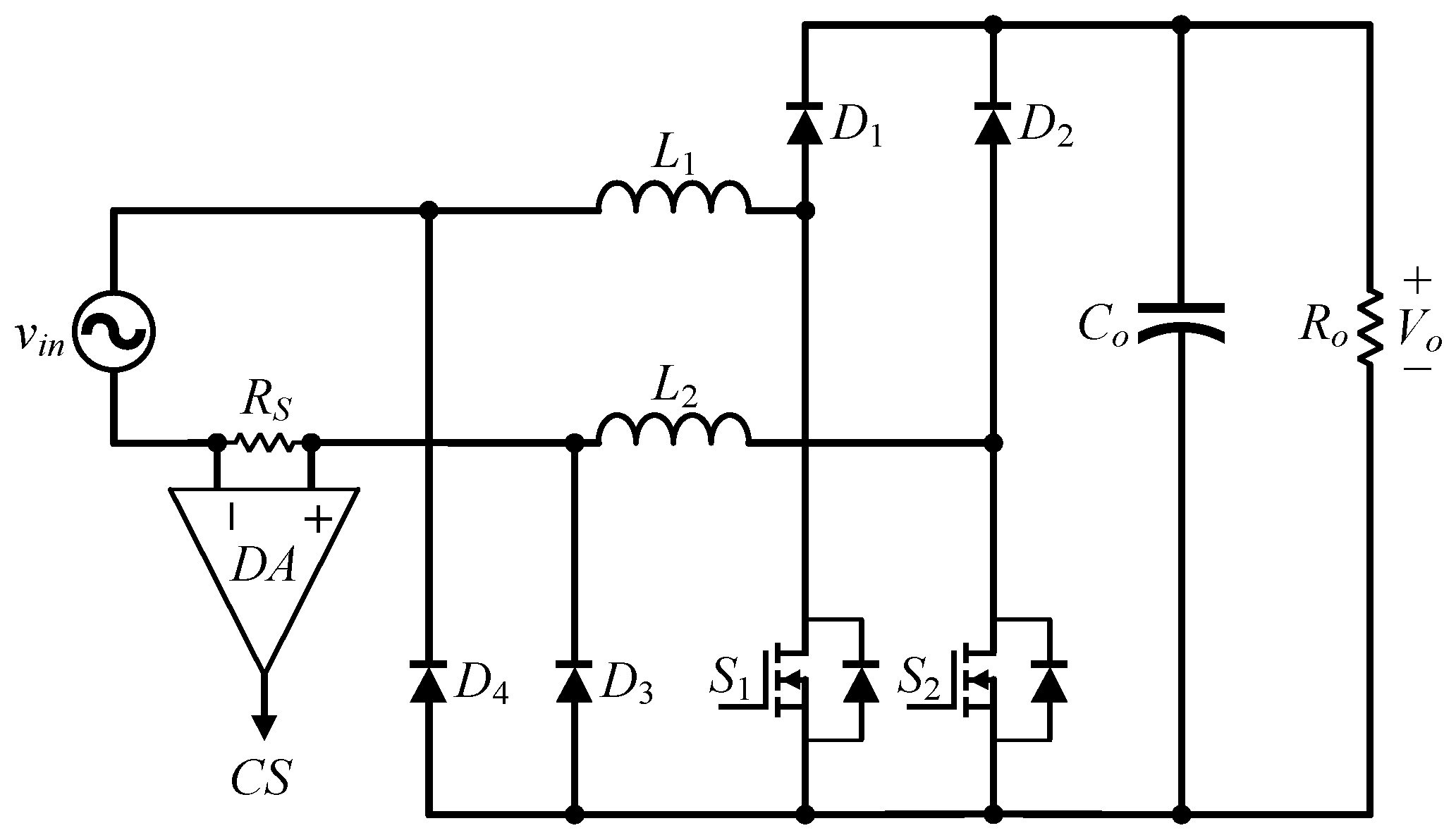
(2) Differential amplifier detection
This method is to connect a current-detecting resistor RS in series with the input, and then to use a differential amplifier DA to detect the inductor current signal on RS, as shown in Figure 4. This method is simple and relatively inexpensive. Since the current-sampling resistor is placed at the negative terminal of the AC input voltage vin, the detected CS is easily interfered with by the common-mode noise, resulting in a relatively low power factor.
(3) Current transformer detection
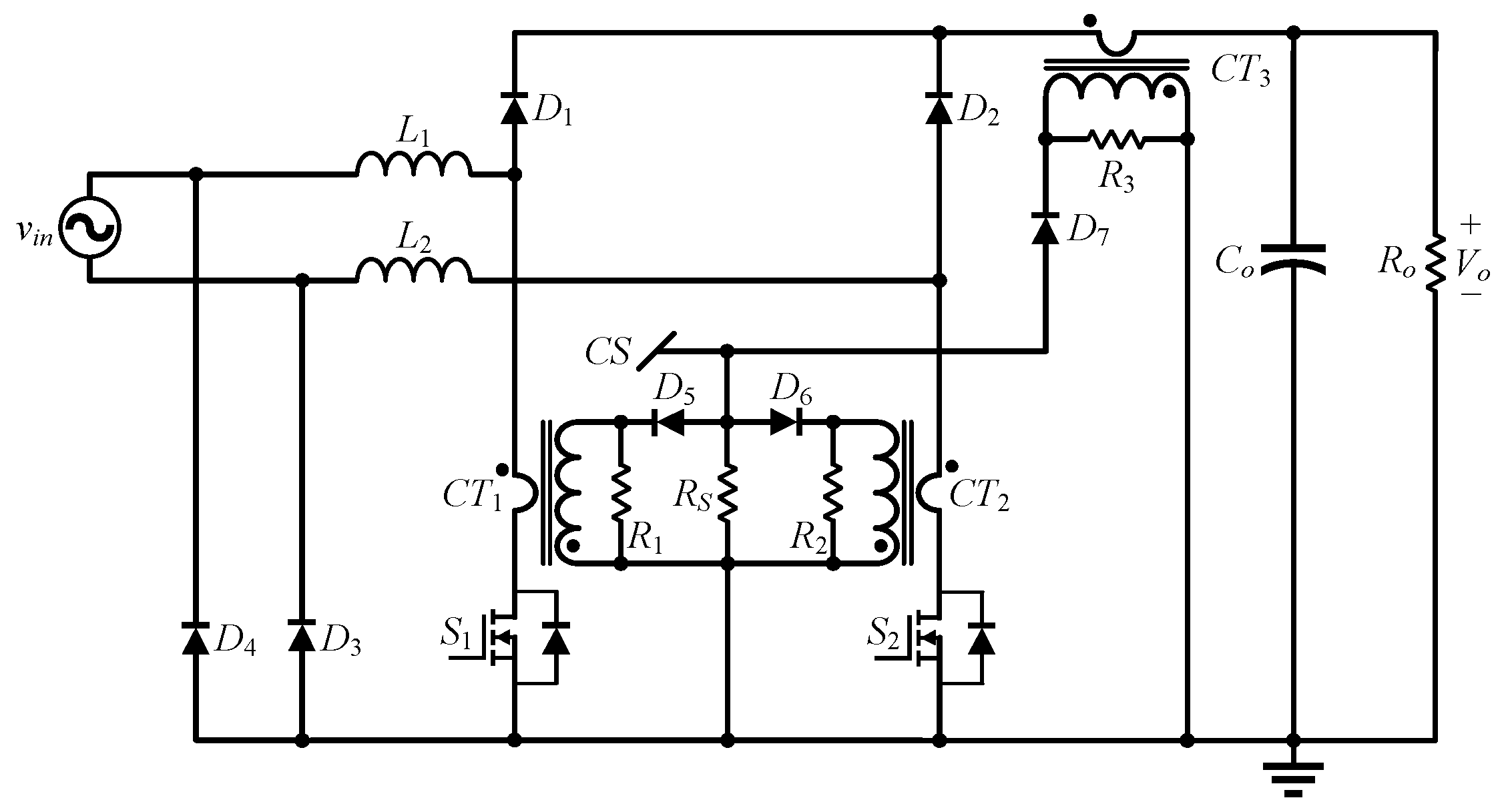
As shown in Figure 5, this method requires the use of three current transformers; the main switch S1 and the main switch S2 are each connected in series with the current transformers CT1 and CT2, the diodes D5 and D6, and the resistors R1 and R2, respectively, whereas the output is also connected in series with the current transformer CT3, the diode D7, and the resistor R3. The following is a brief description of the corresponding operating principle:
(a) When vin > 0, the main switch S1 is turned on, the inductor L1 stores energy, the inductor current flows through the current transformer CT1, and CS is detected. When vin > 0, the main switch S1 is cut off, the inductor L1 releases energy through diode D1, the inductor current flows through current transformer CT3, and CS is detected.
(b) When vin < 0, the main switch S2 is turned on, the inductor L2 stores energy, the inductor current flows through the comparator CT2, and CS is detected. When vin < 0, the main switch S2 is cut off, the inductor L2 releases energy through diode D2, the inductor current flows through current transformer CT3, and CS is detected.
By integrating the detected inductor current signals from the above three current transformers, these inductor current signals are then converted into voltage signals that can be used by the controller via the peripheral circuits. Therefore, this method uses a large number of current transformers and complex peripheral circuits.
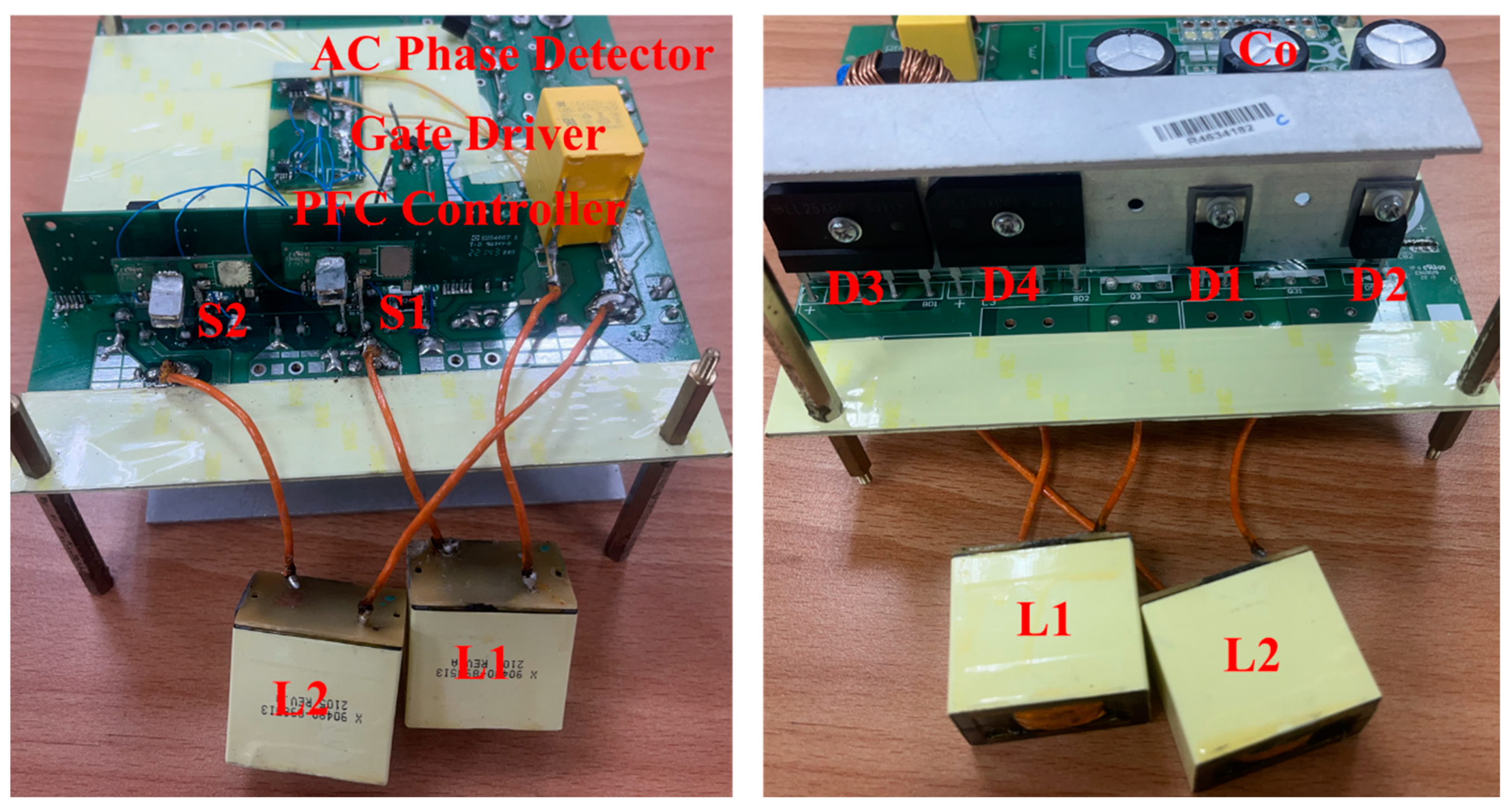
In this paper, our new method is to replace the metal–oxide–semiconductor field-effect transistor (MOSFET) with a gallium nitride field-effect transistor (GaNFET) in the selection of the main switch. The reverse-biased conduction voltage of the third quadrant of the GaNFET is much higher than the forward-biased voltage of the diode, which solves the problem of detecting the inductor current, reduces the number of current sensors, and simplifies the corresponding peripheral circuits and components.

2. Operating Principle of the Semi-Bridgeless PFC Rectifier Using MOSFET Main Switches

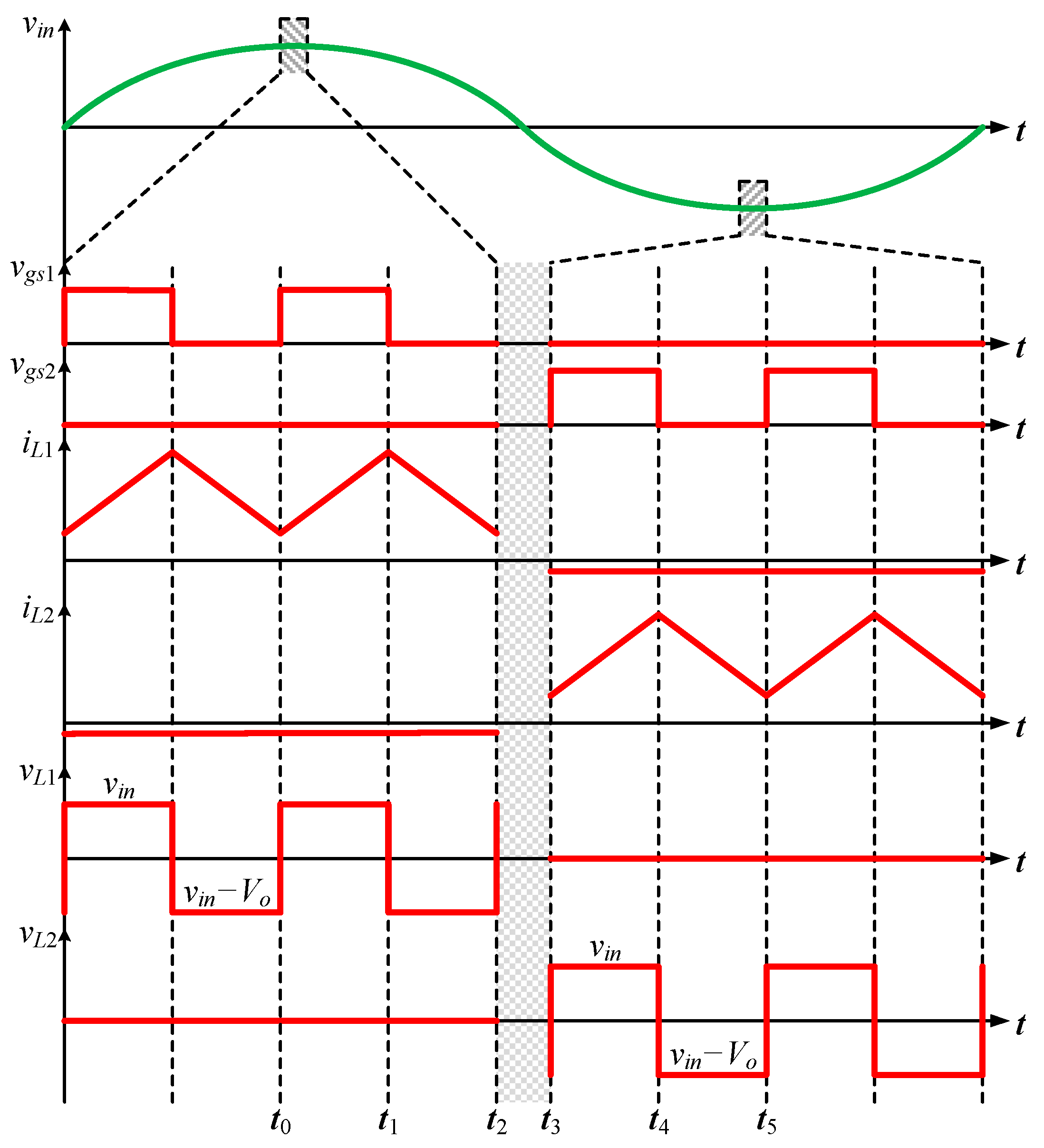
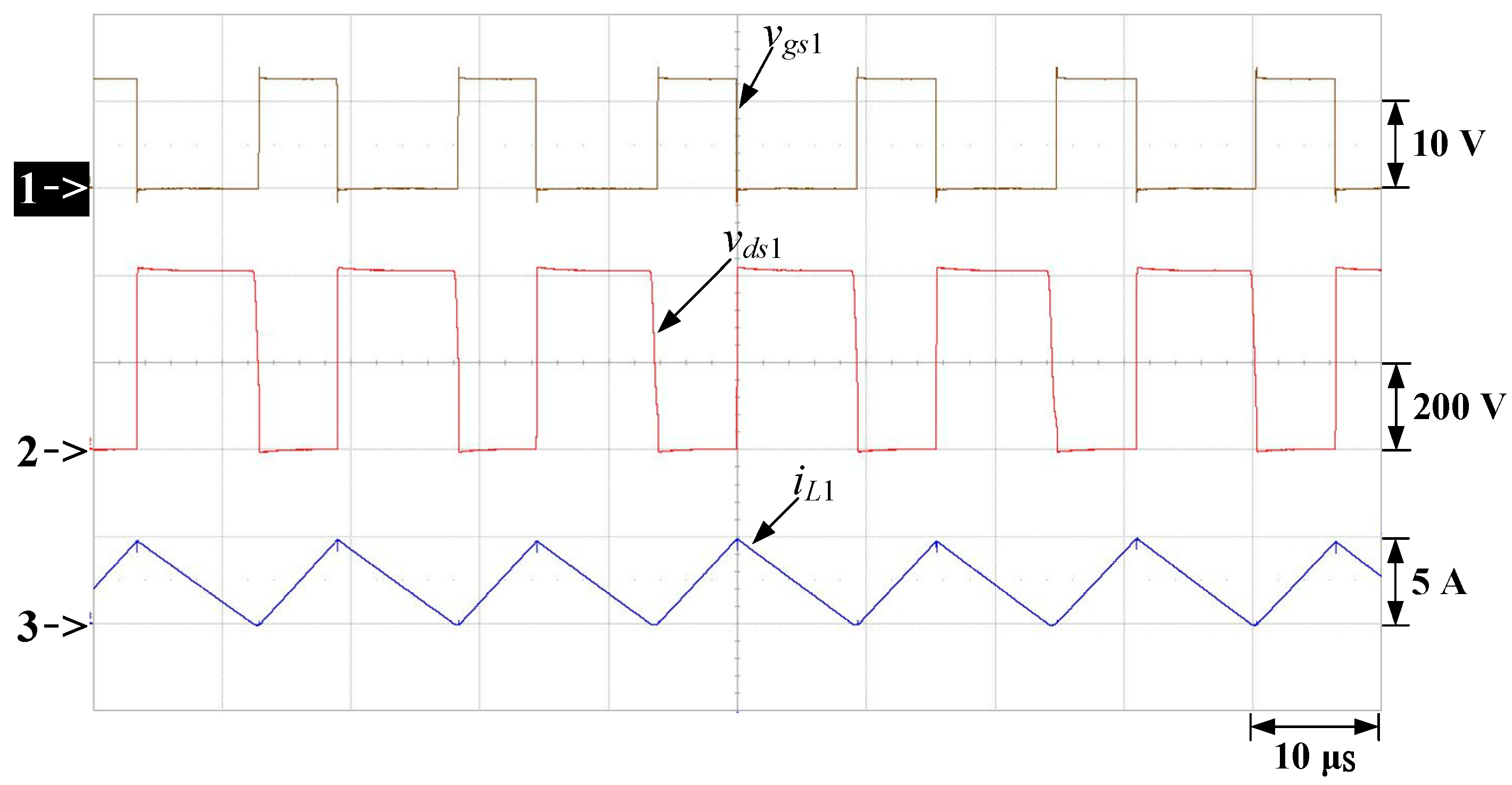
Figure 6 shows the waveforms relevant to the circuit operation during the positive and negative half-cycles of the input AC voltage, as well as these waveforms under high-frequency switching corresponding to the peak value of the sine-wave voltage. From this figure, it can be seen that the circuit has four operating states. When the input AC voltage vin is under the positive half-cycle, the main switch S1 is turned on/off under high-frequency switching and the main switch S2 is always cut off. When the input AC voltage vin is under the negative half-cycle, the main switch S1 is cut off and the main switch S2 is turned on/off under a high switching frequency. There are four operating states for this semi-bridge rectifier, and they are described in the following text.
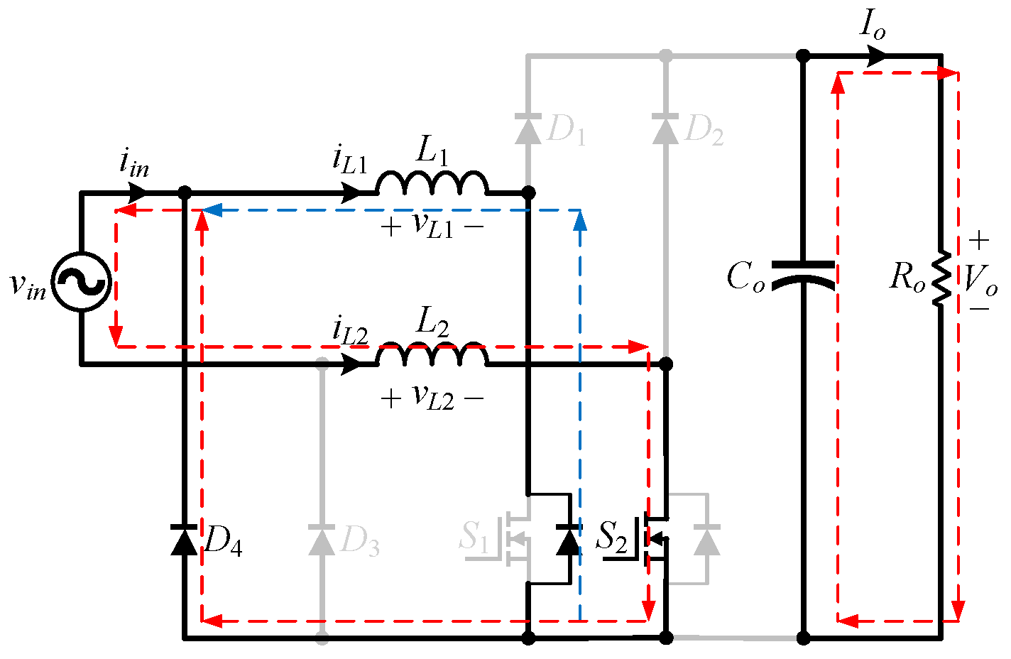
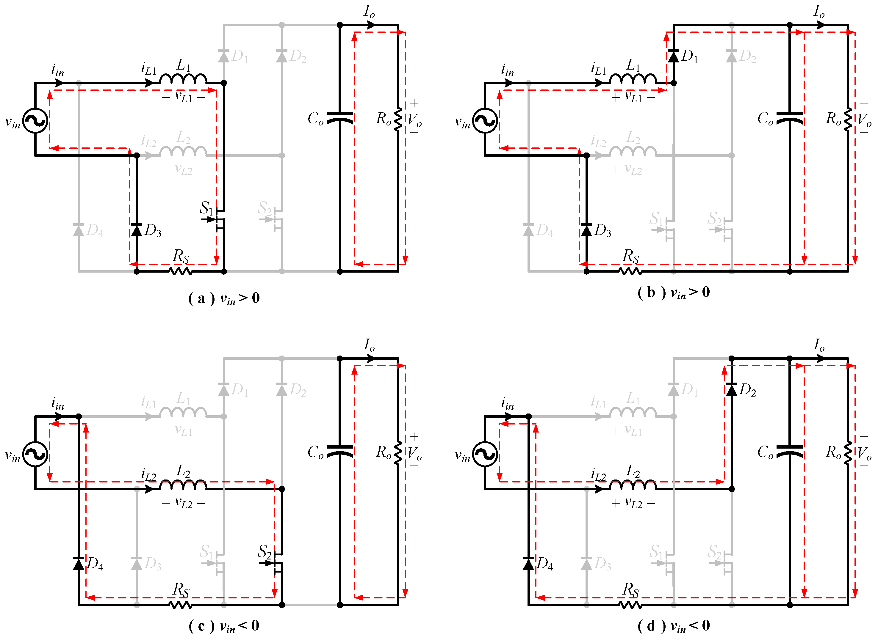
  • State 1: [t0tt1]
As shown in Figure 7, when the input AC voltage vin is under the positive half-cycle, i.e., vin > 0, the main switch S1 conducts, the main switch S2 is cut off, the diode D3 conducts, and the diodes D1, D2, and D4 are all cut off. The input current iin flows through the inductor L1, the main switch S1, and the diode D3, and another small portion of the current flows through the body diode of the main switch S2 and the inductor L2. At the same time, the voltage vL1 across the inductor L1 is the input voltage vin, and the inductor L1 is in a state of magnetization due to the positive voltage across the inductor L1. During this state, the inductor current iL1 rises linearly, and the inductor L1 stores energy. The energy required for the output resistor Ro is supplied by the output capacitor Co.
To speak more lucidly, in Figure 7, the main switch S1 is on, so the body diode of S2 and the diode D3 are both forward-biased; hence, there are two inductor current paths returning to the input voltage vin. One path has the diode D3 connected in series with the inductor L1, whereas the other path has the body diode of S2 connected in series with the inductors L1 and L2. Accordingly, the impedance of the path with the body diode of S2 is higher than that of the path with diode D3, so a small portion of the inductor current will flow through the body diode of S2, and the majority of the inductor current will flow through the diode D3. Note that the switching frequency is much higher than the line frequency. Therefore, the voltage drop due to the line frequency is quite low, so the forward-biased voltage of the body diode of the main switch S1 is similar to the voltage forward-biased voltage of the diode D3, causing the small portion to seem constant.
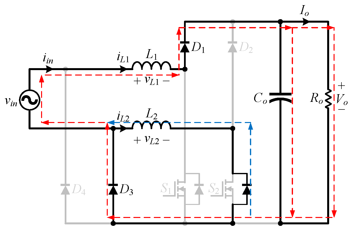
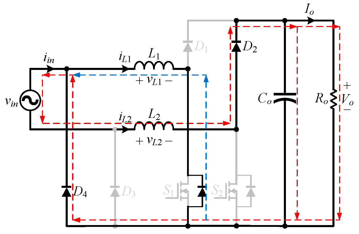
  • State 2: [t1tt2]
As shown in Figure 8, when the input voltage vin is under the positive half-cycle, i.e., vin > 0, the main switches S1 and S2 are cut off, the diodes D1 and D3 are turned on, and the diodes D2 and D4 are cut off. The input current iin flows through the inductor L1, the diodes D1 and D3, the output capacitor Co, and the output resistor Ro, and another small portion of the current flows through the body diode of the main switch S2 and the inductor L2. At the same time, the voltage vL1 across the inductor L1 is the input voltage vin minus the output voltage Vo, and the inductor L1 is in a state of demagnetization due to the negative voltage across the inductor L1. During this state, the inductor current iL1 decreases linearly and the inductor L1 releases energy. The energy required for the output resistor Ro is supplied by the input voltage vin and the inductor L1, which also charge the output capacitor Co.
  • State 3: [t3tt4]
As shown in Figure 9, when the input AC voltage vin is under the negative half-cycle, i.e., vin < 0, the main switch S1 is cut off, the main switch S2 conducts, the diode D4 is turned on, and the diodes D1, D2, and D3 are all cut off. The input current iin flows through the inductor L2, the main switch S2, and the diode D4, and another small portion of the current flows through the body diode of the main switch S1 and the inductor L1. At the same time, the voltage vL2 across the inductor L2 is the input voltage vin, and the inductor L2 is in a state of magnetization due to the positive voltage across the inductor L2. During this state, the inductor current iL2 rises linearly, and the inductor L2 stores energy. The energy required for the output resistor Ro is supplied by the output capacitor Co.
  • State 4: [t4tt5]
As shown in Figure 10, when the input AC voltage vin is under the negative half-cycle, i.e., vin < 0, the main switches S1 and S2 are cut off, the diodes D2 and D4 are turned on, and the diodes D1 and D3 are cut off. The input current iin flows through the inductor L2, the diodes D2 and D4, the output capacitor Co, and the output resistor Ro, and a small portion of the current flows through the body diode of the main switch S1 and the inductor L1. At the same time, the voltage vL2 across the inductor L2 is the input voltage vin minus the output voltage Vo, and the inductor L2 is in a state of demagnetization due to the negative voltage across the inductor L2. During this state, the inductor current iL2 decreases linearly, and the inductor L2 releases energy. The energy required for the output resistor Ro is supplied by the input voltage vin and the inductor L2, which charge the output capacitor Co.

3. Current Sensor Improvement Based on a GaNFET

In the following subsections, we will mainly discuss how to reduce the number of current sensors.

3.1. Operational Characteristics of the GaNFET in the Third Quadrant

From the literature [31], it can be seen that the structure of the GaNFET has a channel that generates two-dimensional electron gas (2DEG) by connecting the source and drain electrodes, and the gate voltage is used to control the conductivity of this channel, as shown in Figure 11.
To speak lucidly, there are three operating cases for the GaNFET in Figure 11, as described below, where Vth is the threshold voltage and Ron is the channel’s turn-on resistance:
Case 1: As Vgs > Vth and VDS > 0, the channel is turned on. The current IDS is operated in the first and third quadrants, and this operation feature is the same as that of the MOSFET. The corresponding drain–source voltage VDS equation, called the forward-biased conduction voltage, can be expressed as follows:
V D S = I D S R o n
Case 2: As Vgs < Vth and VDS > 0, the channel is turned off. The current IDS is not operated in the first quadrant, and this is the same as for the MOSFET.
Case 3: As Vgs < Vth and VDS < 0, the channel has a chance to be turned on, with IDS operated in the third quadrant. The corresponding source–drain voltage VSD equation, called the reverse-biased conduction voltage, can be expressed as follows:
V S D ( V t h V g s ) + I S D R o n
As compared with the MOSFET, since VDS < 0, the body diode of the MOSFET will be turned on and operated in the third quadrant, with a forward-biased voltage of about 0.6 V to 1.5 V, but without (2). But the GaNFET has a relatively high reverse-biased conduction voltage VSD, with the voltage VthVgs typically being higher than 0.6 V when the voltage Vgs is set to zero. For example, the threshold voltage Vth of a commercially available 650 V GaNFET is about 1.7 V. Therefore, the improvement proposed in this paper is to utilize the fact that the reverse-biased conduction voltage VSD of the GaNFET is higher than the forward-biased conduction voltage VDS of the diode when the GaNFET is operated in the third quadrant.
The operating range of VDS for the GaNFET is based on industrial applications. The blue line is suitable for bidirectional operation, for example, battery charging and discharging, whereas the red line is suitable for regenerative operations, for example, motor regeneration (Figure 12).

3.2. Current Flow with GaNFETs Used as Main Switches

In this paper, a method is proposed to improve the inductor current detection for semi-bridgeless PFC rectifiers by replacing the MOSFET main switches with the GaNFET main switches shown in Figure 7. As shown in [31], the reverse-biased conduction voltage VSD of the GaNFET main switches S1 and S2 in the third quadrant is much higher than the forward-biased voltage of the diodes D3 and D4, such that there is no inductor current flowing through the inactivated main switch and the inductor. The key to this improvement lies in the fact that there is only one inductor current path at any time, and it only necessary to connect a current-detecting resistor RS in series between the sources of the GaNFET main switches S1 and S2 and the anodes of the diodes D3 and D4, as shown in Figure 13. Accordingly, the voltage across the current-detecting resistor RS contains information on the real inductor current. In this way, the inductor current can be accurately detected, thus reducing the number of current sensors and simplifying the corresponding peripheral circuits and components.

4. Design Considerations

In this section, the system configuration adopted, the system specifications defined, and the component specifications used will be described, along with the GaNFET main switches used.

4.1. System Configuration Adopted

Figure 14 shows the overall system configuration of the semi-bridgeless PFC rectifier. This system consists of the main power stage circuit, input voltage divider, output voltage divider, current-sensing resistor RS, AC phase detector, gate drivers, and PFC controller.
From Figure 14, it can be seen that the output voltage is sensed by the voltage divider. Also, from this figure, it can be seen that the PFC controller adopts the average current-mode control, i.e., dual-loop control. For the voltage loop control to be considered, the output voltage signal is measured by the output voltage divider and subtracted from the voltage reference, and then the error value and the measured input voltage signal are fed into the waveform generator to create the current command value in phase with the mains voltage. For the current loop control to be considered, the inductor current signal measured by the current-sensing resistor RS is subtracted from this command value, so as to yield the desired control force. For each switching cycle, the control system calculates the turn-on time of the main switch so that the input current will be controlled in phase with the input voltage as tightly as possible, thereby resulting in a relatively high power factor and relatively low current harmonics.

4.2. System Specifications Defined

Table 1 displays the system specifications for the semi-bridgeless PFC rectifier.

4.3. Component Specifications Used

Table 2 displays the component specifications used in the semi-bridgeless PFC rectifier.

5. Experimental Results

Some measured waveforms and data are given to verify the effectiveness of the proposed method.

5.1. Measured Steady-State Waveforms

Some steady-state waveforms were measured at rated loads under input voltages of AC 90, 115, 230, and 264 V. The input voltage and inductor current were measured as shown in Figure 15, Figure 16, Figure 17 and Figure 18. From these waveforms, it can be seen that there is no inductor current flowing through the inactivated main switch and the inductor during the time when the inductor stores and releases energy.
Next, the input voltage and input current were measured as shown in Figure 19, Figure 20, Figure 21 and Figure 22. From these waveforms, it can be seen that the input current tightly follows the input voltage, so that the power factor correction can be achieved.
After this, the gate driving signal, main switch voltage, and inductor current were measured at AC voltage peaks as shown in Figure 23, Figure 24, Figure 25 and Figure 26, and there was no voltage spike on the main switches. Therefore, from these abovementioned waveforms, it can be seen that the outputs are stable at rated loads for the whole range of input voltage.

5.2. Measured Dynamic Response Waveforms

Next, we measured some dynamic response waveforms relevant to the output current, output voltage, and input current at different input voltages due to upload and download, as shown in Figure 27, Figure 28, Figure 29 and Figure 30. The input voltages were AC 90, 115, 230 and 264 V, and the output loads were varied from 20% of the rated load to the rated load and from the rated load to 20% of the rated load. From these waveforms, it can be seen that from 20% of the rated load to the rated load, the corresponding change in output voltage is about 6.5%, with a recovery time of about 150 ms, while from the rated load to 20% of the rated load, the corresponding change in output voltage is about 4.5%, with a recovery time of about 75 ms.
From the waveforms shown in Section 5.1 and Section 5.2, it can be seen that the effectiveness of the semi-bridgeless PFC rectifier with GaNFET main switches can be verified.

5.3. Measured Data

Next, the power factor PF, total harmonic distortion THD, input power Pin, and output power Pout from the rated load to 10% of the rated load, in 10% intervals, were measured under input voltages of AC 115 and 230 V, as shown in Table 3 and Table 4. In addition, based on Pin and Pout, the efficiency Eff. can be calculated. Based on Table 3 and Table 4, the curves of PF vs. load current, THD vs. load current, and Eff. vs. load current were plotted as shown in Figure 31, Figure 32 and Figure 33, respectively. According to these experimental results, under an input voltage of AC 115 V and the rated output power, the PF is 0.994 and the efficiency is 96.42%, whereas under an input voltage of AC 230 V and the rated output power, the PF is 0.996 and the efficiency is 98.45%. Accordingly, this semi-bridgeless PFC rectifier prototype possesses high PF and high efficiency.
Finally, a digital power analyzer (Chroma 66202), manufactured by Chroma Inc., Taoyuan City, Taiwan, was used to measure the harmonic values of the input currents at rated loads under input voltages of AC 115 and 230 V. The test values and the limit values of IEC61000-3-2 Class D were tabulated, as shown in Table 5 and Table 6. Figure 34 and Figure 35 were plotted based on these two tables. From these two figures, it can be seen that the semi-bridgeless PFC rectifier prototype meets the IEC 61000-3-2 Class D harmonic standard.

5.4. Experimental Setup

Figure 36 displays a photo of the prototype for testing.

6. Conclusions

In this paper, the problem of detecting the inductor current of a semi-bridgeless PFC rectifier was improved. Firstly, we introduced the GaNFET feature that the reverse-biased conduction voltage VSD in the third quadrant is higher than the forward-biased conduction voltage of the diode. This feature was used to improve the current-detecting circuit. Accordingly, a semi-bridgeless PFC rectifier prototype was implemented to demonstrate the effectiveness of the proposed strategy.
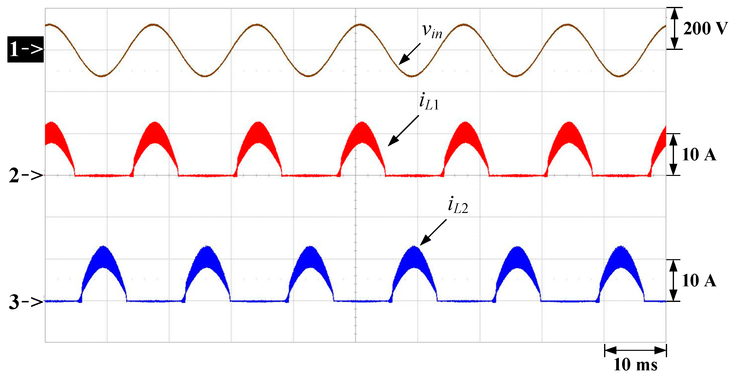
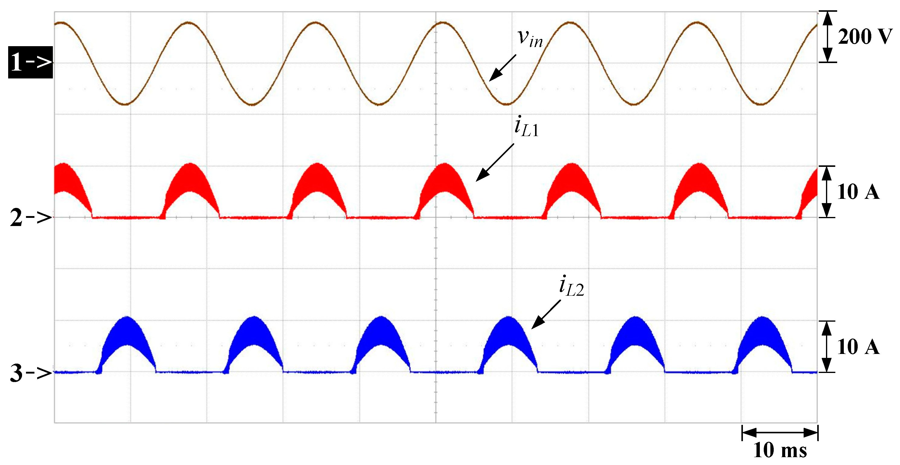
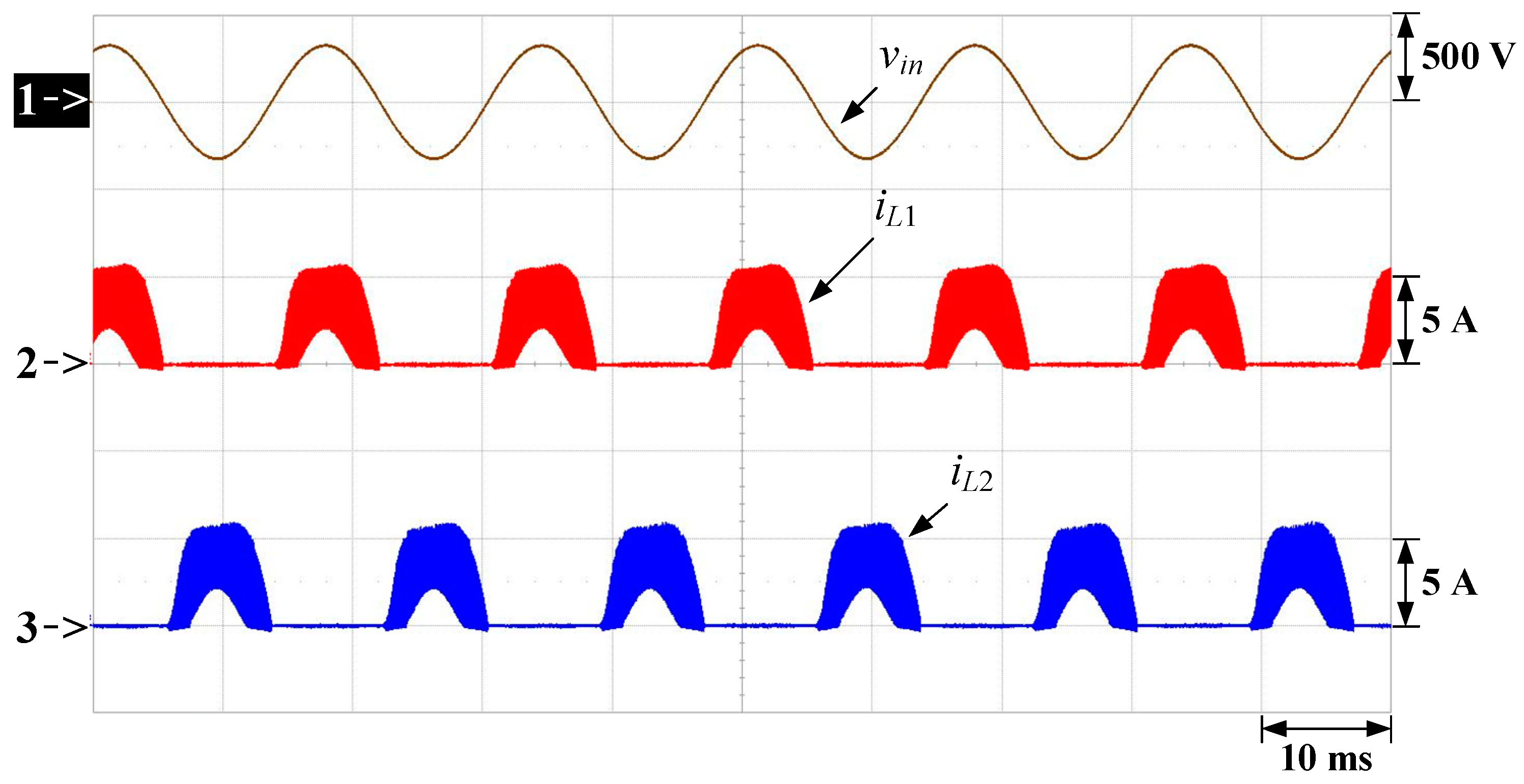
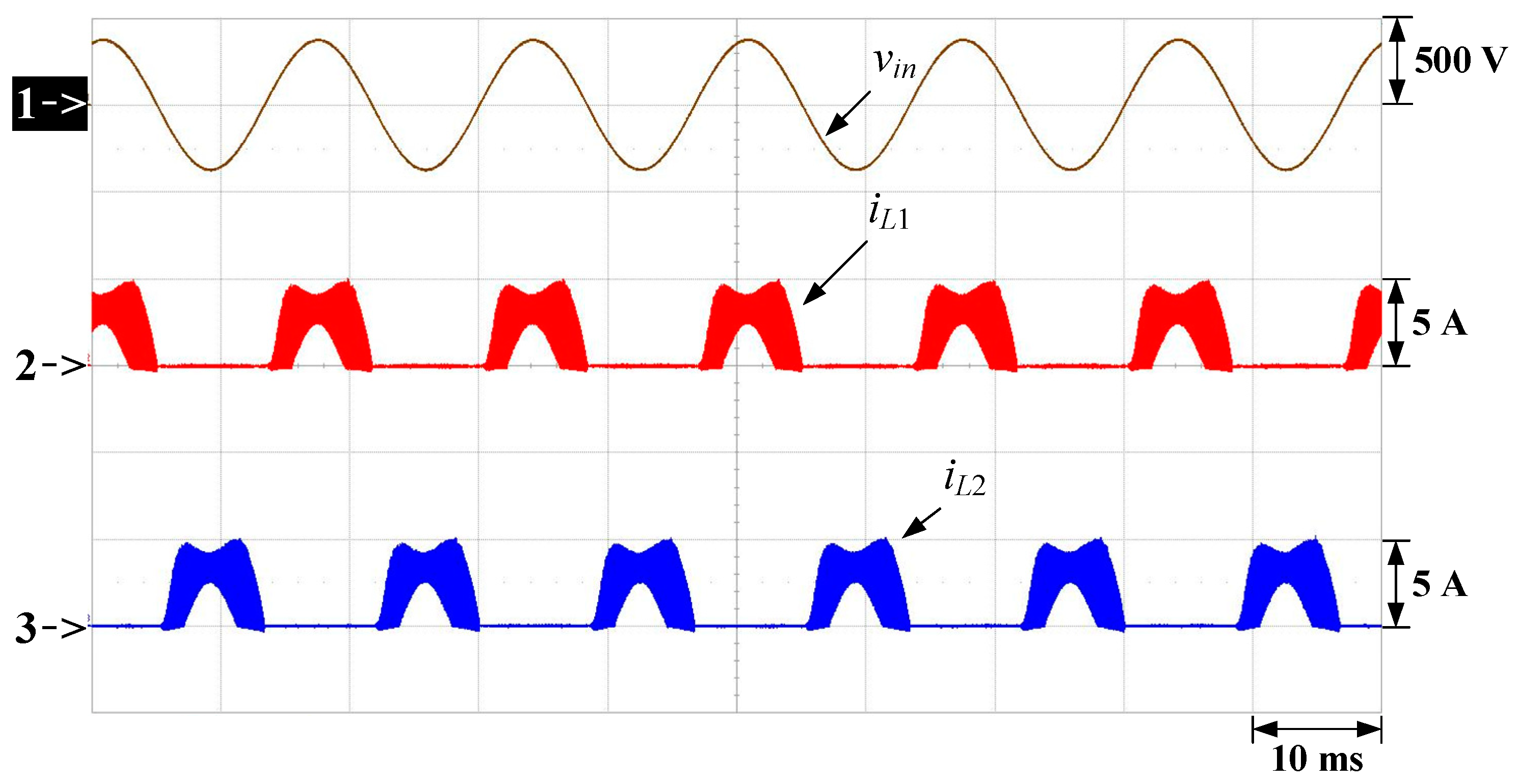
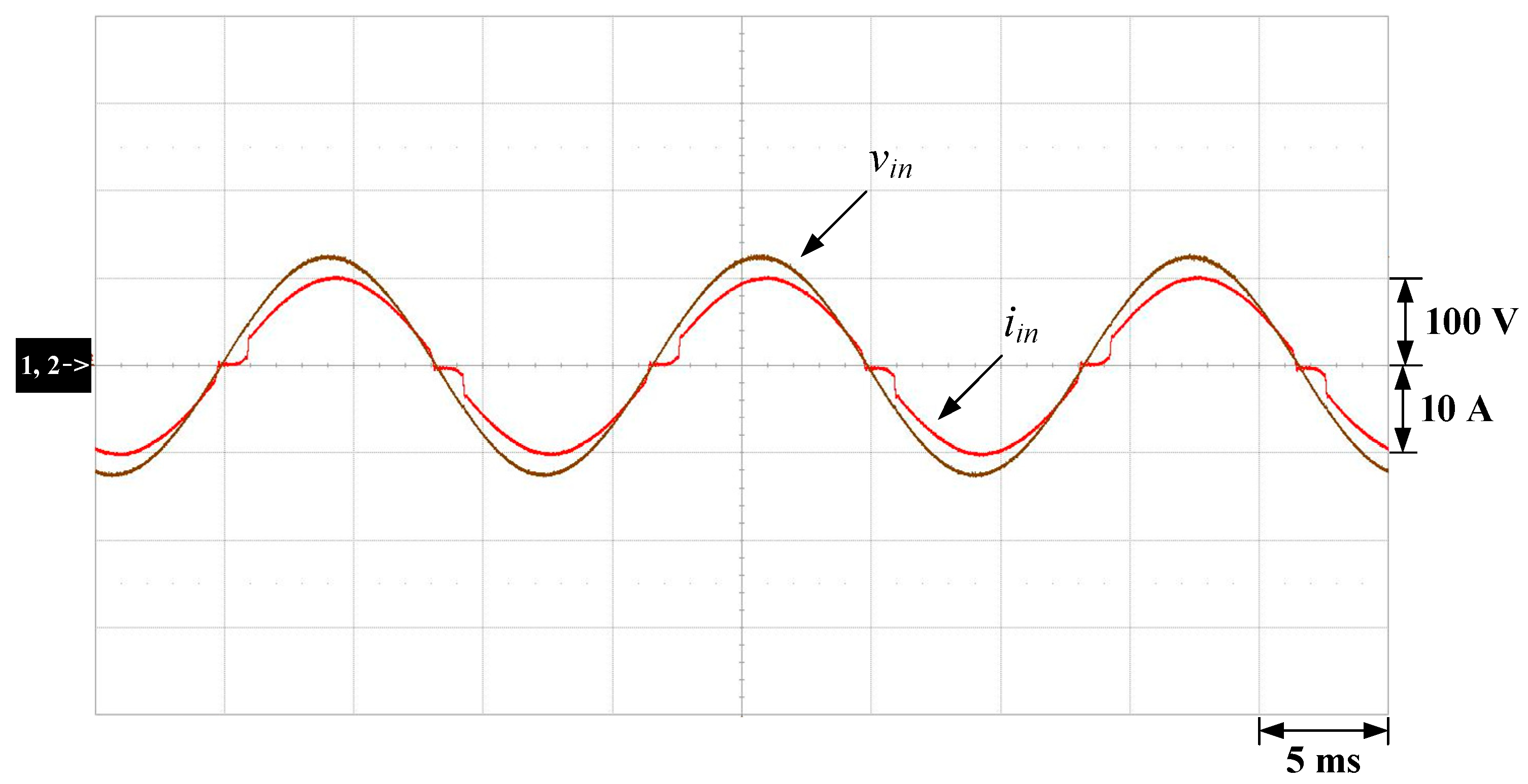
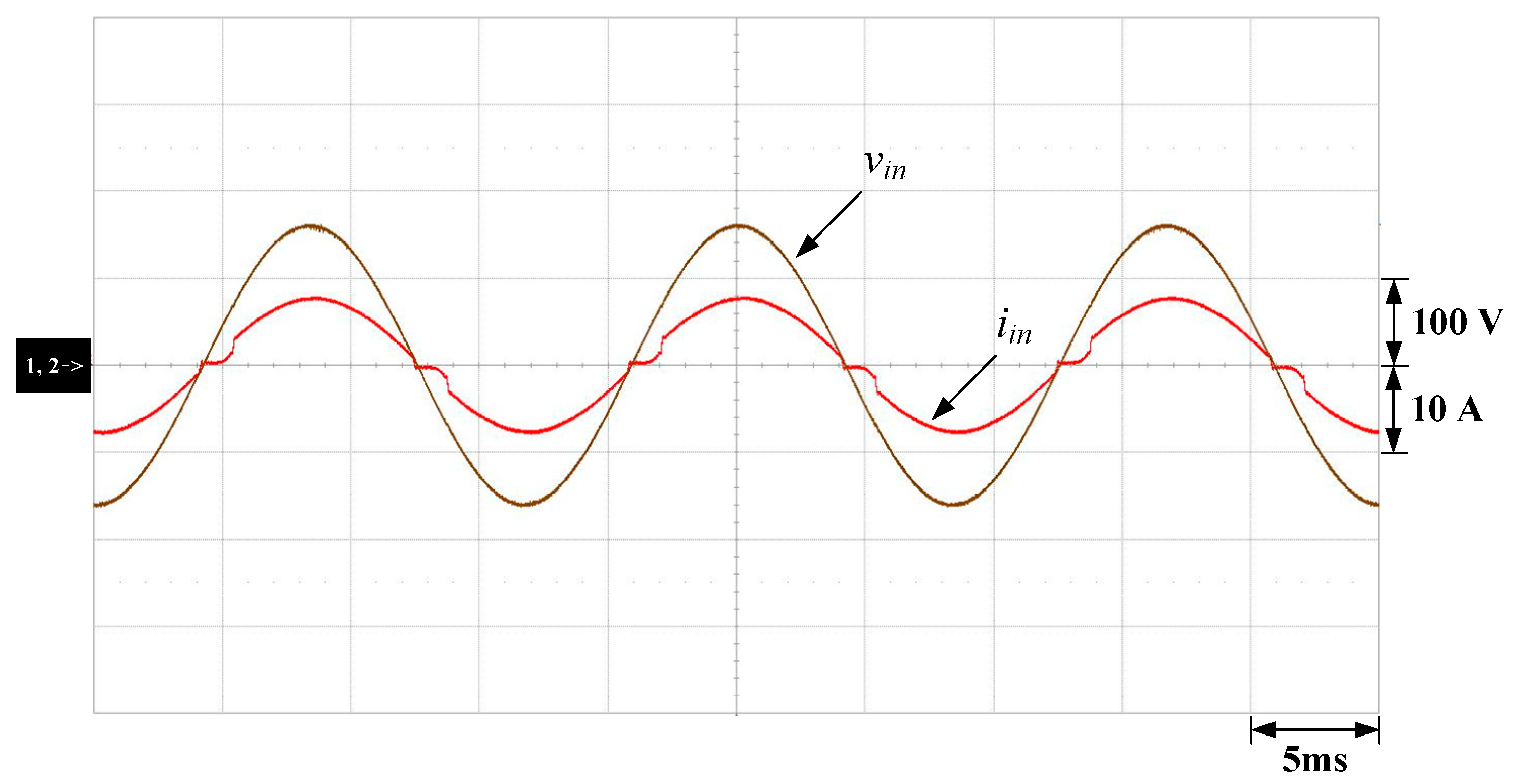
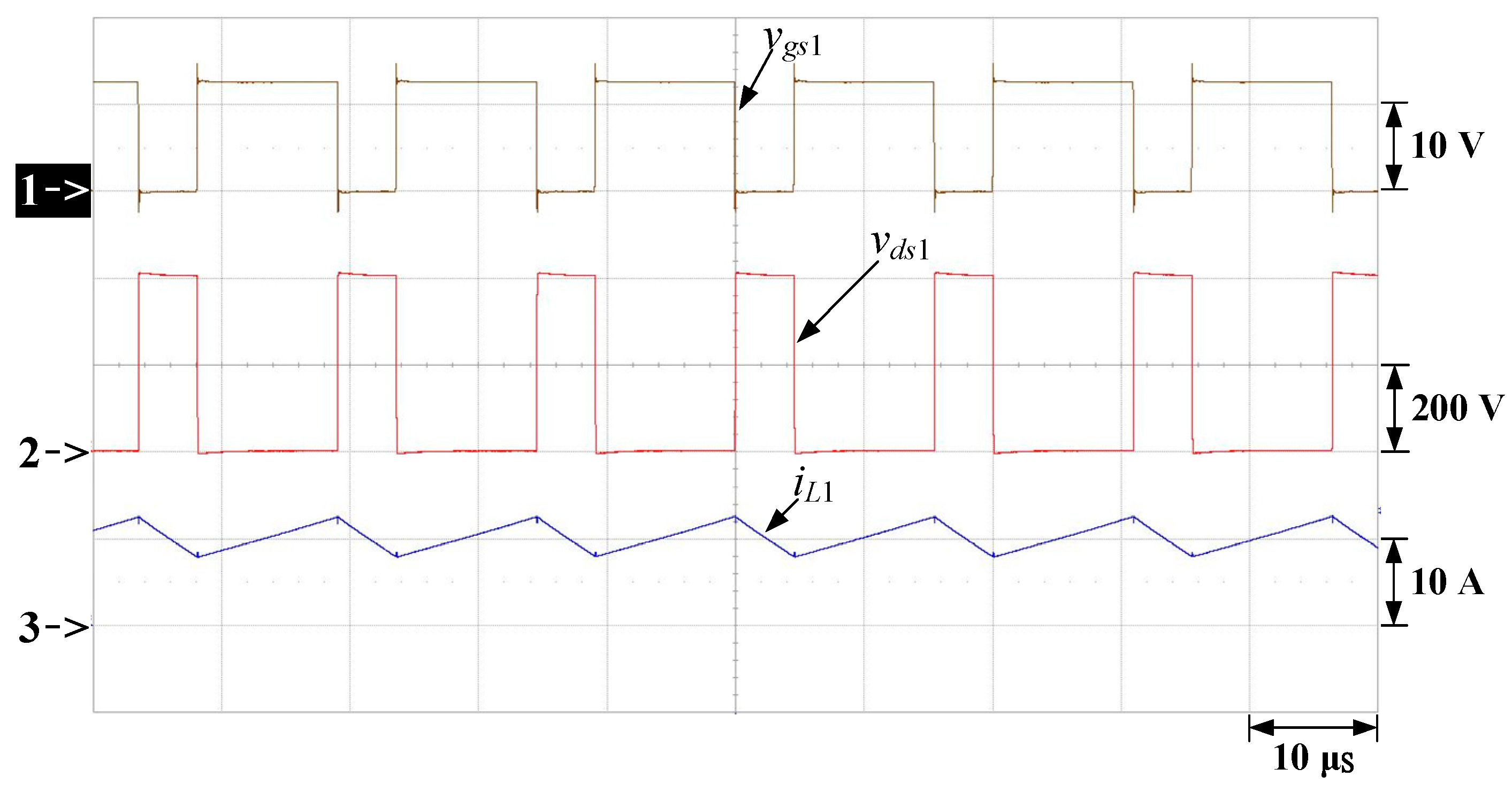
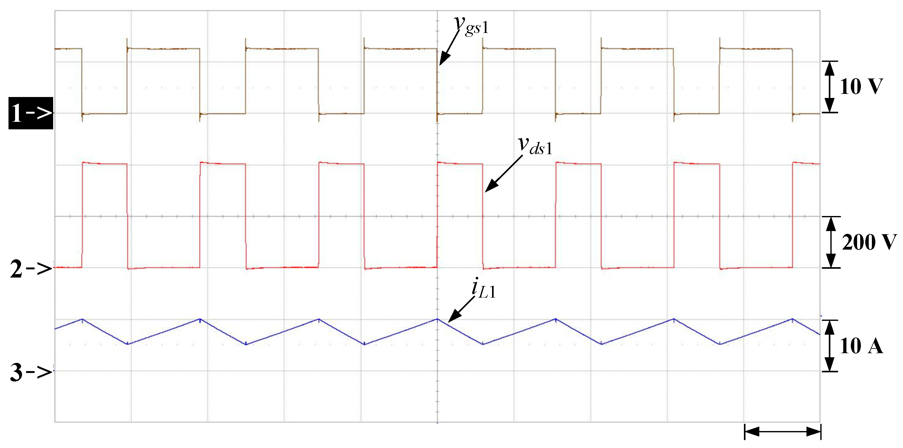
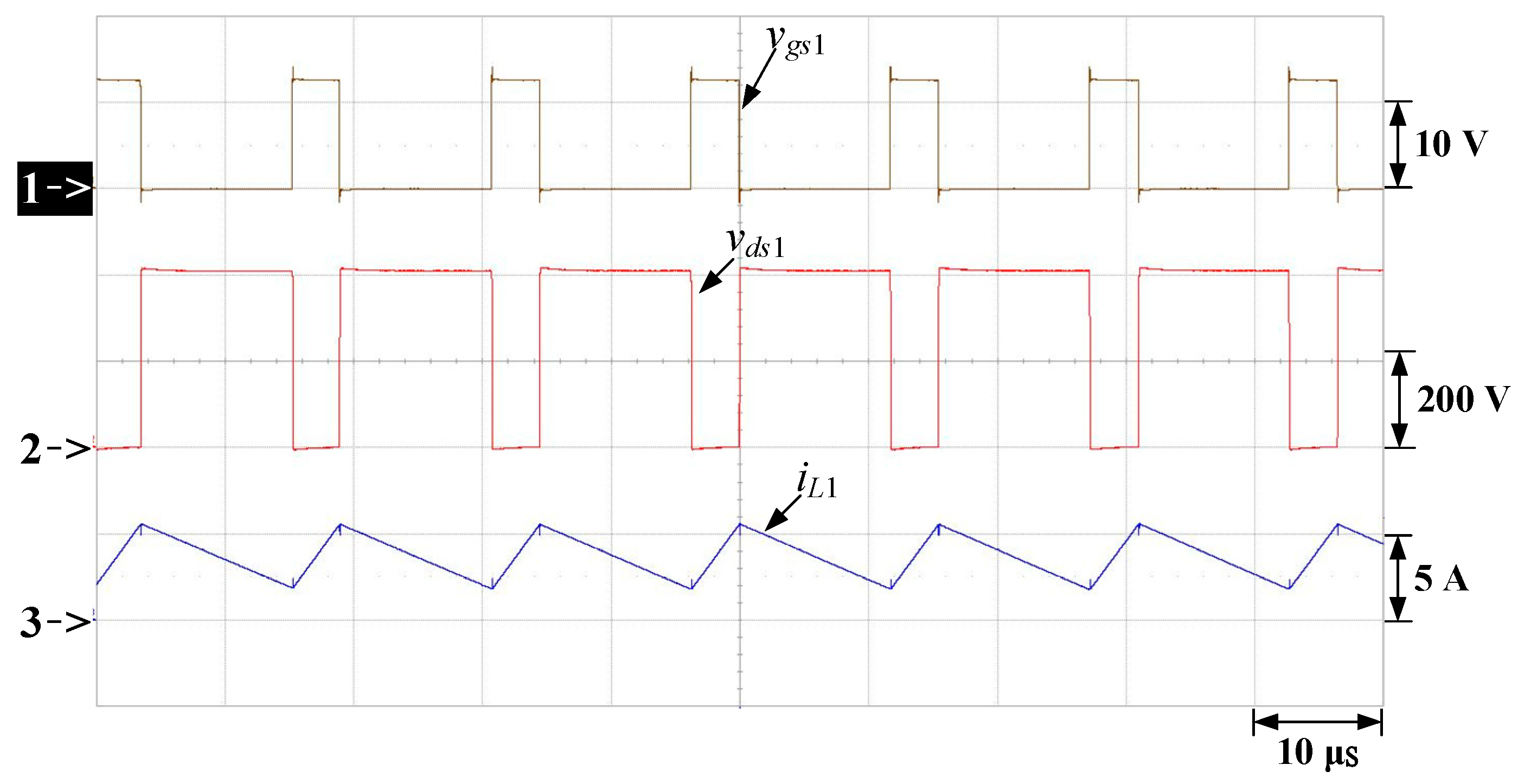
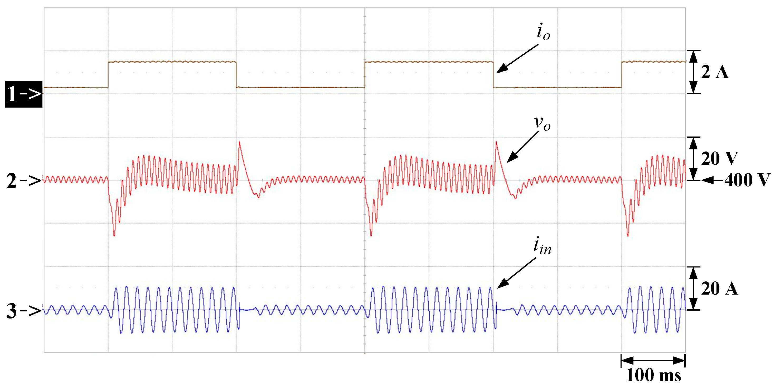
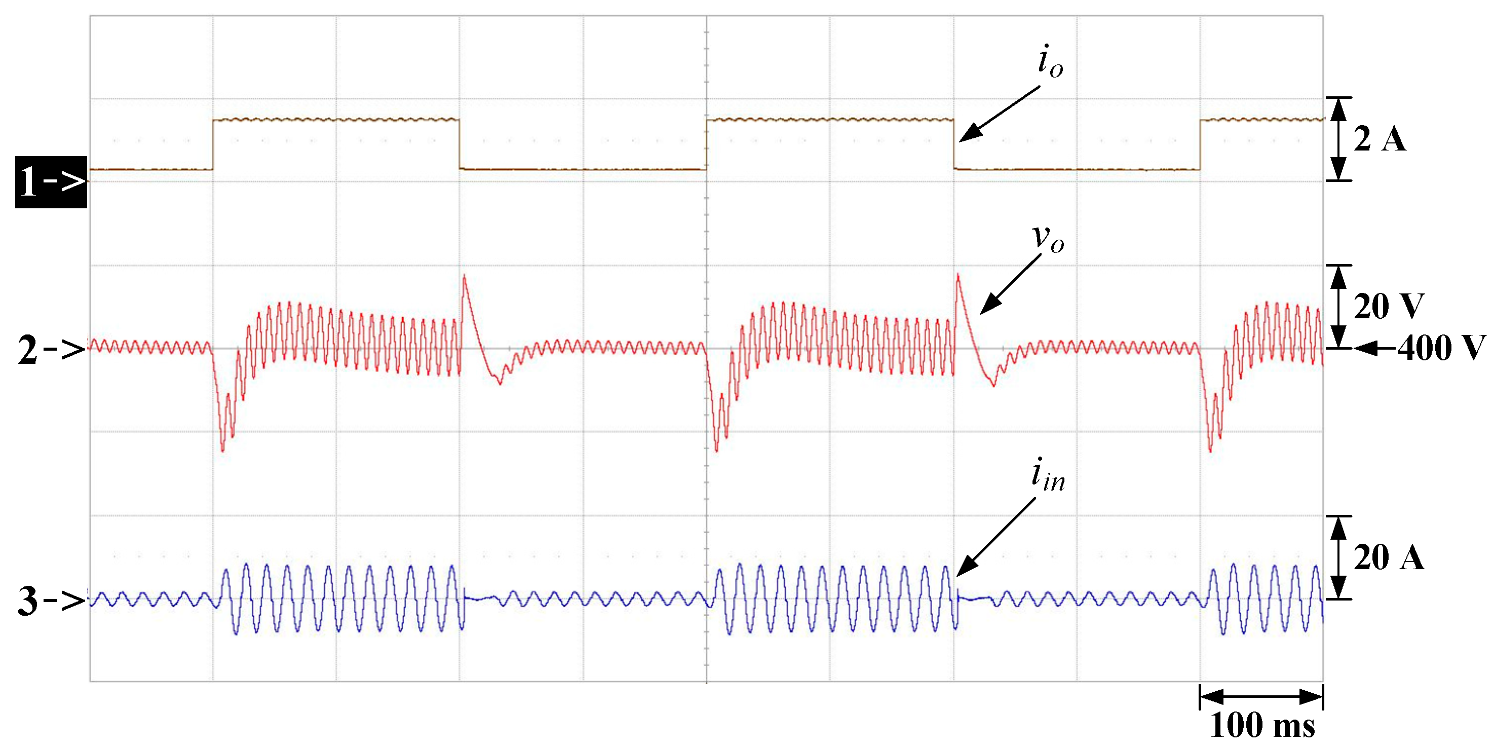
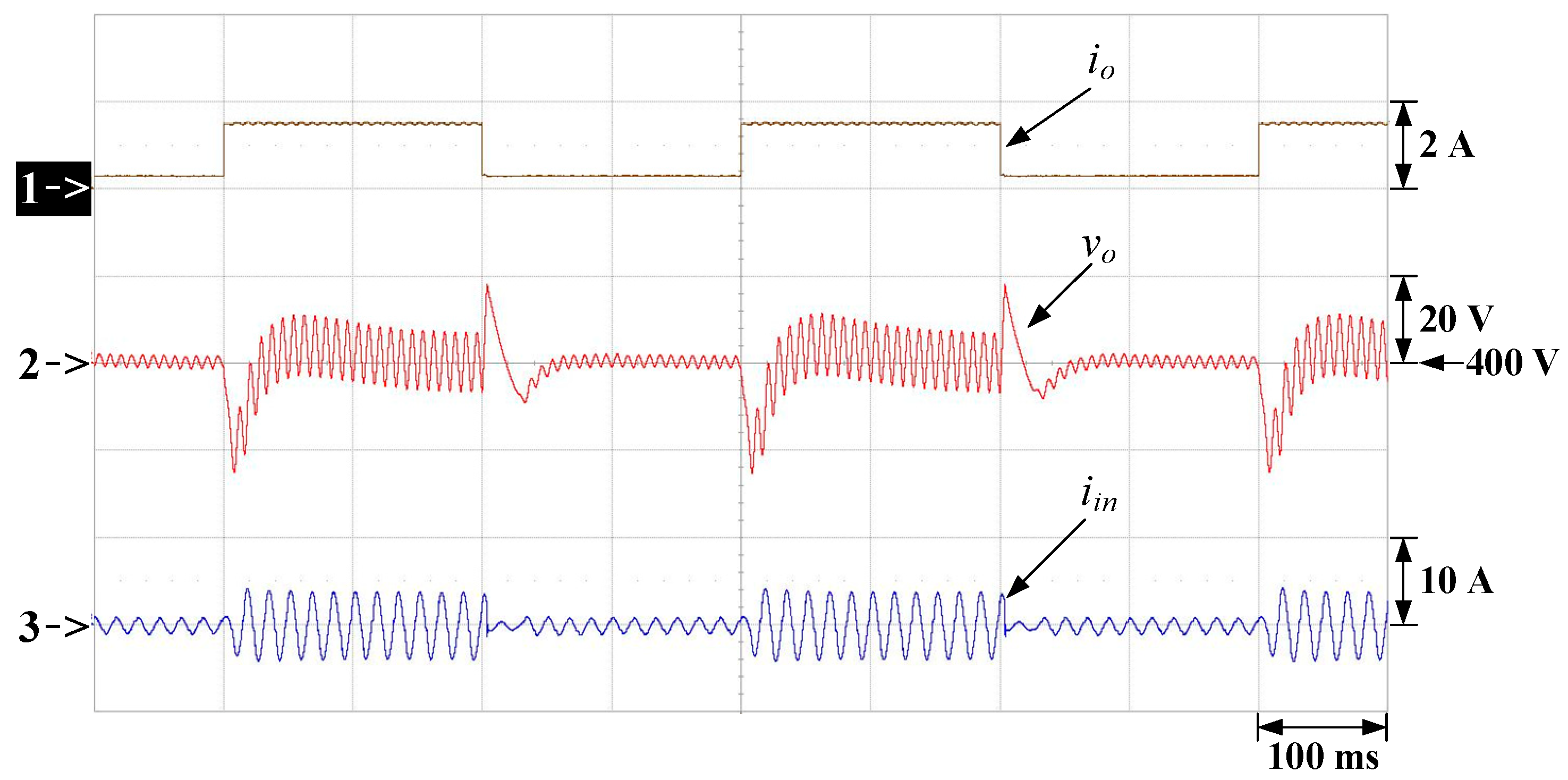
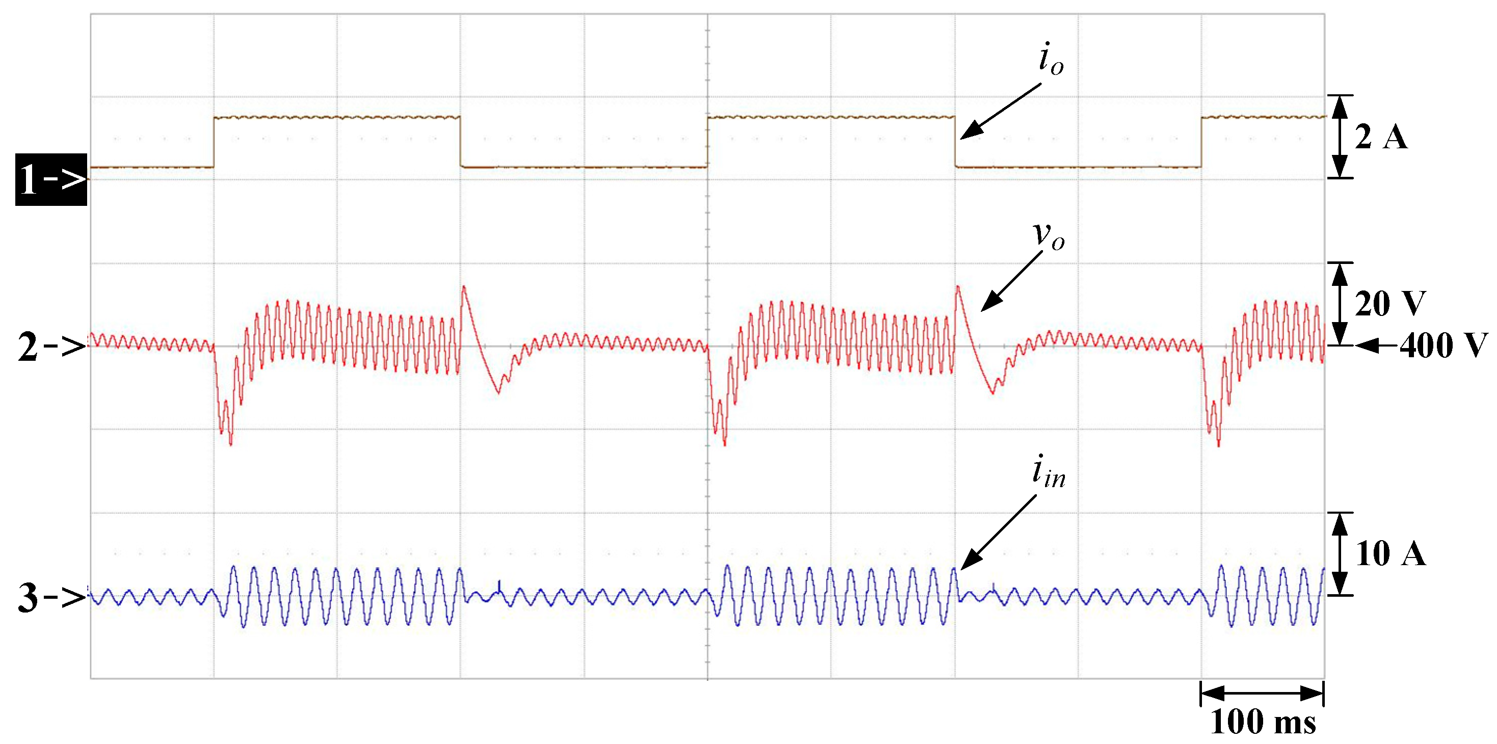
From the experimental results, it can be seen that under different input voltages and output power ratings, the inductor current path has only one loop and does not flow through the inactivated main switch and the inductor. It was confirmed that the proposed strategy is effective, thereby reducing the number of current sensors and simplifying the number of peripheral circuits and components.
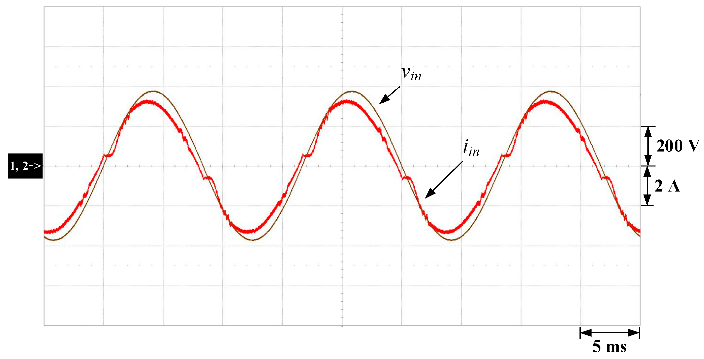
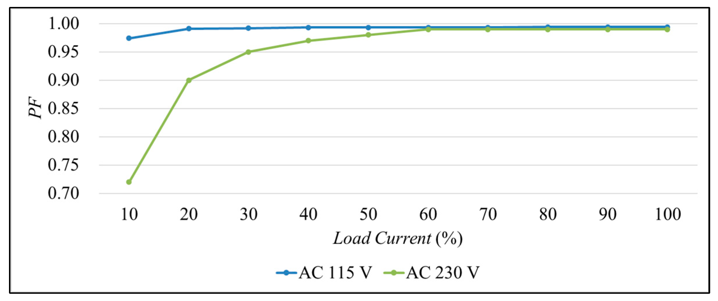
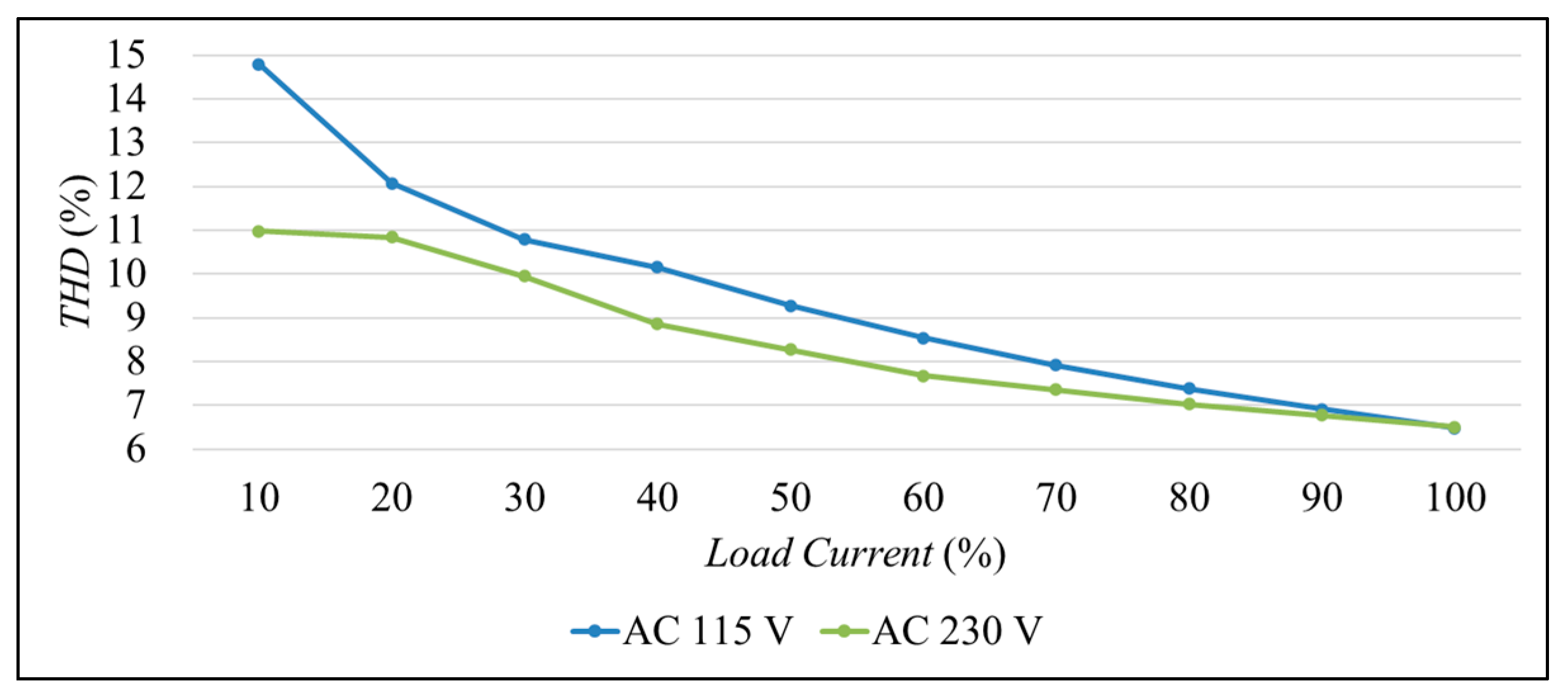
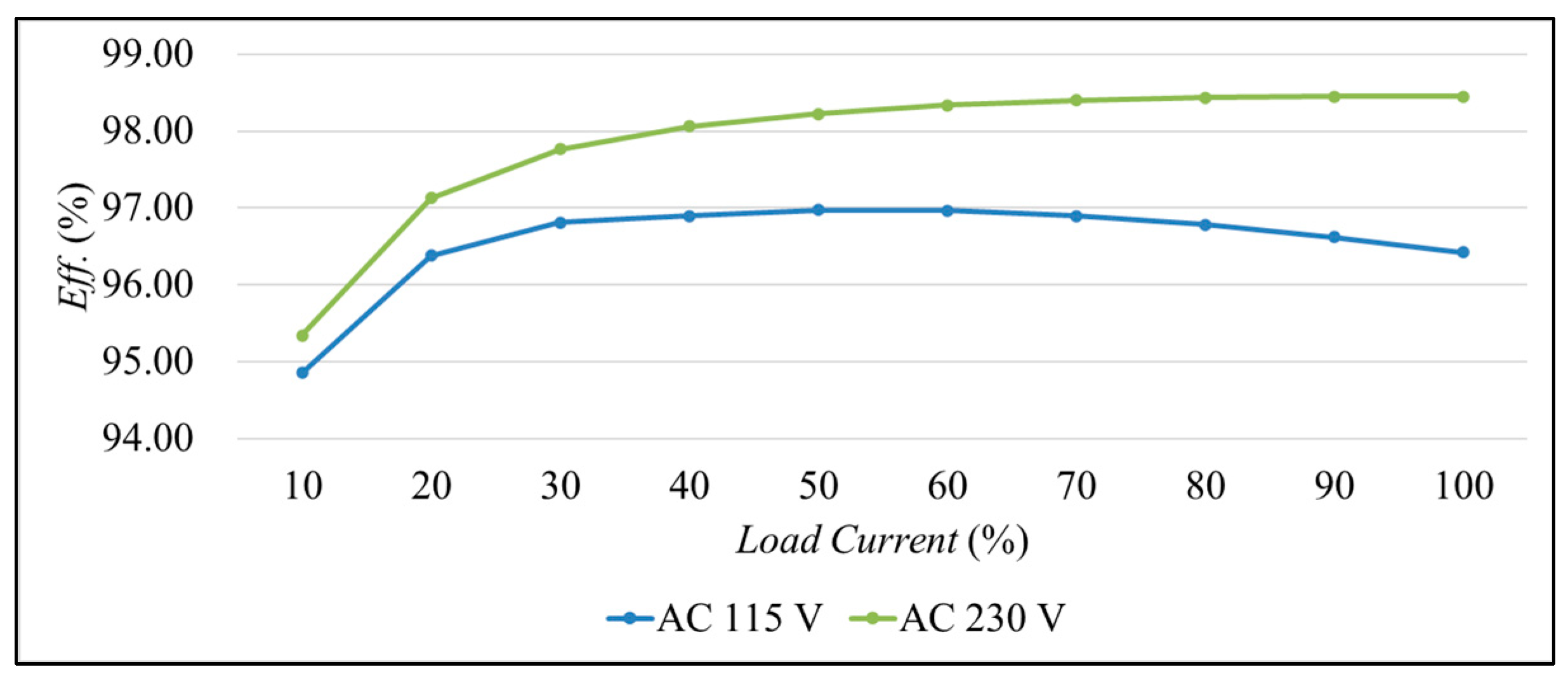
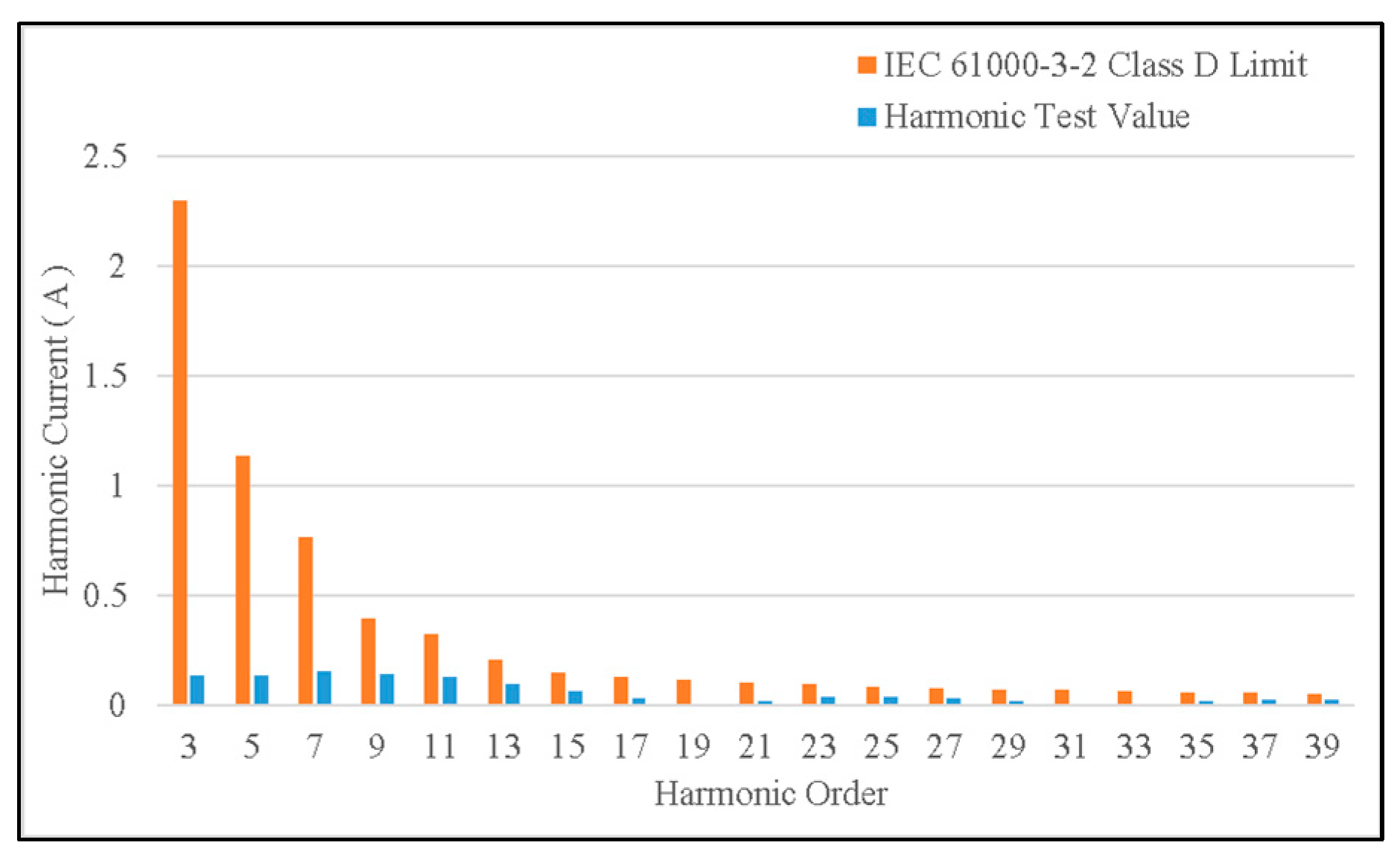
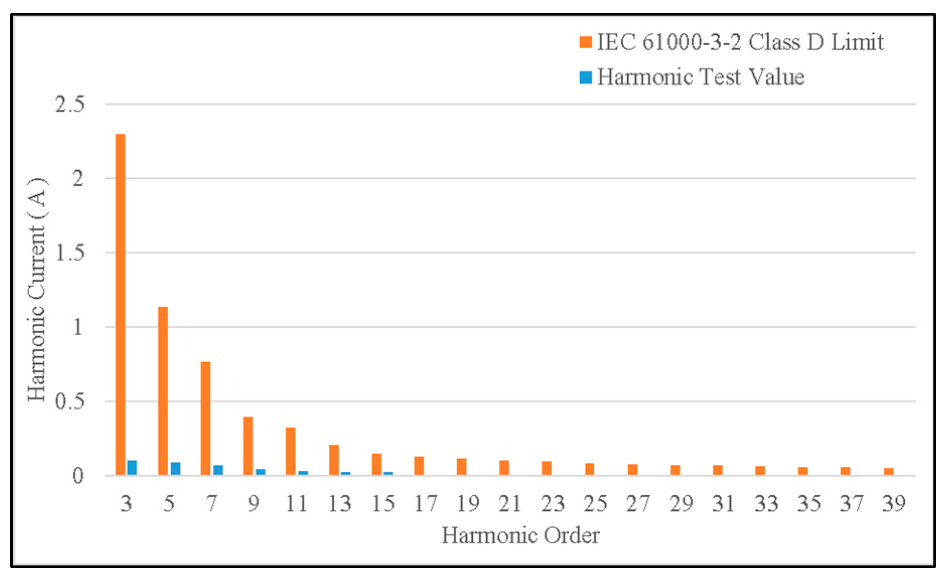
Furthermore, under an input voltage of AC 115 V and the rated output power, the PF is 0.994 and the efficiency is 96.42%, whereas under an input voltage of AC 230 V and the rated output power, the PF is 0.996 and the efficiency is 98.45%. This confirms that the semi-bridgeless PFC rectifier prototype with GaNFET main switches possesses high PF and high efficiency. Moreover, the IEC61000-3-2 Class D current harmonic standard can be met under both of these two cases.

Author Contributions

Conceptualization, C.-B.Y. and K.-I.H.; methodology, C.-B.Y.; validation, C.-B.Y.; formal analysis, C.-B.Y. and K.-I.H.; investigation, C.-B.Y.; resources, K.-I.H.; data curation, C.-B.Y.; writing—original draft preparation, C.-B.Y. and K.-I.H.; writing—review and editing, K.-I.H.; visualization, C.-B.Y.; supervision, K.-I.H.; project administration, K.-I.H.; funding acquisition, K.-I.H. All authors have read and agreed to the published version of the manuscript.

Funding

This research was funded by the Ministry of Science and Technology, Taiwan, under the grant number NSTC 112-2221-E-027-015-MY2.

Data Availability Statement

No new data were created or analyzed in this study. Data sharing is not applicable to this article.

Conflicts of Interest

The authors declare no conflict of interest.

References

  1. Mansoor, A.; Grady, W.M.; Thallam, R.S.; Doyle, M.T.; Krein, S.D.; Samotyj, M.J. Effect of supply voltage harmonics on the input current of single-phase diode bridge rectifier loads. IEEE Trans. Power Deliv. 1995, 10, 1416–1422. [Google Scholar] [CrossRef]
  2. Sainz, L.; Pedra, J.; Mesas, J.J. Single-phase full-wave rectifier study with experimental measurements. Electr. Power Syst. Res. 2007, 77, 339–351. [Google Scholar] [CrossRef]
  3. Najafi, E.; Vahedi, A.; Mahanfar, A.; Yatim, A.H.M. A new controlling method based on peak current mode (PCM) for PFC. In Proceedings of the IEEE 2nd International Power and Energy Conference, Johor Bahru, Malaysia, 1–3 December 2008; pp. 1103–1107. [Google Scholar]
  4. IEC 61000-3-2; Harmonics Standards Overview. Schaffner EMC Inc.: Edison, NJ, USA, 2006.
  5. Bhattacharyya, S.; Cobben, J.F.G.; Kling, W.L. Harmonic current pollution in a low voltage network. In Proceedings of the IEEE PES General Meeting’10, Minneapolis, MN, USA, 25–29 July 2010; pp. 1–8. [Google Scholar]
  6. Meyer, J.; Blanco, A.-M.; Domagk, M.; Schegner, P. Assessment of prevailing harmonic current emission in public low-voltage networks. IEEE Trans. Power Deliv. 2017, 32, 962–970. [Google Scholar] [CrossRef]
  7. Azazi, H.Z.; El-Kholy, E.E.; Mahmoudi, S.A.; Shokalla, S.S. Review of passive and active circuits for power factor correction in single phase low power AC-DC converter. In Proceedings of the 14th International Middle-East Power Systems Conference-MEPCON (MEPCON’10), Giza Governorate, Egypt, 19–21 December 2010; pp. 217–224. [Google Scholar]
  8. Mitchell, D.M. AC-DC Converter Having an Improved Power Factor. U.S. Patent 4,412,277, 25 October 1983. [Google Scholar]
  9. Moriconi, U. A bridgeless PFC configuration based on L4981 PFC controller. In Application Note AN 1606; STMicroelectronics: Geneva, Switzerland, 1 November 2002. [Google Scholar]
  10. Etz, R.; Patarau, T.; Petreus, D. Comparison between digital average current mode control and digital one cycle control for a bridgeless PFC boost converter. In Proceedings of the 2012 IEEE 18th International Symposium for Design and Technology in Electronic Packaging (SIITME), Alba Iulia, Romania, 25–28 October 2012; IEEE SIITME’12. pp. 211–215. [Google Scholar]
  11. Smedley, K.M.; Cuk, S. One-cycle control of switching converters. IEEE Trans. Power Electron. 1995, 10, 625–633. [Google Scholar] [CrossRef]
  12. Wang, C.-M. A novel zero-voltage-switching PWM boost rectifier with high power factor and low conduction losses. IEEE Trans. Ind. Electron. 2005, 52, 427–435. [Google Scholar] [CrossRef]
  13. Lu, B.; Brown, R.; Soldano, M. Bridgeless PFC implementation using one cycle control technique. In Proceedings of the Twentieth Annual IEEE Applied Power Electronics Conference and Exposition, Austin, TX, USA, 6–10 March 2005; IEEE APEC’05. pp. 812–817. [Google Scholar]
  14. Kong, P.; Wang, S.; Lee, F.C. Common mode EMI noise suppression in bridgeless boost PFC converter. In Proceedings of the APEC 07—Twenty-Second Annual IEEE Applied Power Electronics Conference and Exposition, Anaheim, CA, USA, 25 February–1 March 2007; IEEE APEC’07. pp. 929–935. [Google Scholar]
  15. Masumoto, K.; Shi, K.; Shoyama, M.; Tomioka, S. Comparative study on efficiency and switching noise of bridgeless PFC circuits. In Proceedings of the 2013 IEEE 10th International Conference on Power Electronics and Drive Systems (PEDS), Kitakyushu, Japan, 22–25 April 2013; IEEE PEDS’13. pp. 613–618. [Google Scholar]
  16. Huber, L.; Jang, Y.; Jovanovic, M.M. Performance evaluation of bridgeless PFC boost rectifiers. IEEE Trans. Power Electron. 2008, 23, 1381–1390. [Google Scholar] [CrossRef]
  17. Darly, S.S.; Ranjan, P.V.; Bindu, K.V.; Rabi, B.J. A novel dual boost rectifier for power factor improvement. In Proceedings of the 2011 1st International Conference on Electrical Energy Systems, Newport Beach, CA, USA, 3–5 January 2011; IEEE ICEES’11. pp. 122–127. [Google Scholar]
  18. Sudheer, L.; Kanimozhi, G.; Sreedevi, V.T. Integrator controlled semi-bridgelesss PFC boost converter. In Proceedings of the 2015 International Conference on Circuits, Power and Computing Technologies [ICCPCT-2015], Nagercoil, India, 19–20 March 2015; IEEE ICCPCT’15. pp. 1–6. [Google Scholar]
  19. Hussain, S.A.; Kanimozhi, G. Linear peak current mode control of semi bridgeless AC-DC converter. Indian J. Sci. Technol. 2016, 9, 1–6. [Google Scholar]
  20. Chen, S.-J.; Liang, T.-J.; Tseng, W.-J.; Liu, P.-Y. Design and implementation of a DSP controlled bridgeless power factor corrector. In Proceedings of the 2018 Asian Conference on Energy, Power and Transportation Electrification (ACEPT), Singapore, 30 October–2 November 2018; IEEE ACEPT’18. pp. 1–7. [Google Scholar]
  21. Rajasekar, S.; Karthikeyan, V.; Kumaresan, N. Experimental validation of CCM and DCM operations of semi-bridgeless boost rectifier for power quality improvement in UPS system. In Proceedings of the 2018 20th National Power Systems Conference (NPSC), Tiruchirappalli, India, 14–16 December 2018; IEEE NPSC’18. pp. 1–6. [Google Scholar]
  22. Hawkins, N.A.; McIntyre, M.L.; Latham, J.A. Nonlinear control for power factor correction of a dual-boost bridgeless circuit. In Proceedings of the IECON 2018—44th Annual Conference of the IEEE Industrial Electronics Society, Washington, DC, USA, 21–23 October 2018; IEEE IECON’18. pp. 1368–1373. [Google Scholar]
  23. Perez, M.C.G.; Mahdavi, M.; Amyotte, M.; Glitz, E.S.; Ordonez, M. Power losses estimation on a semi-bridgeless PFC using response surface methodology. In Proceedings of the 2018 IEEE Energy Conversion Congress and Exposition (ECCE), Portland, OR, USA, 23–27 September 2018; IEEE ECCE’18. pp. 2873–2878. [Google Scholar]
  24. Wang, Q.; Cai, F.; Miao, Z. A bridgeless dual boost PFC converter with power decoupling based on model predictive current control. In Proceedings of the 2019 4th International Conference on Intelligent Green Building and Smart Grid (IGBSG), Hubei, China, 6–9 September 2019; IEEE IGBSG’19. pp. 397–400. [Google Scholar]
  25. Jalan, S.K.; Gupta, N. Bridgeless boost rectifier as front end converter (FEC) in uninterruptible power supply (UPS) applications for improving power quality issues. In Proceedings of the 2019 IEEE 1st International Conference on Energy, Systems and Information Processing (ICESIP), Chennai, India, 4–6 July 2019; IEEE ICESIP’19. pp. 1–6. [Google Scholar]
  26. Dacol, R.P.; Heerdt, J.A.; Waltrich, G. Non-isolated high current battery charger with PFC semi-bridgeless rectifier. In Proceedings of the 2019 IEEE 15th Brazilian Power Electronics Conference and 5th IEEE Southern Power Electronics Confer-ence (COBEP/SPEC), Santos, Brazil, 1–4 December 2019; IEEE COBEP/SPEC’19. pp. 1–6. [Google Scholar]
  27. Tseng, S.; Fan, J. Bridgeless boost converter with an interleaving manner for PFC applications. Electronics 2021, 10, 296. [Google Scholar] [CrossRef]
  28. Ortiz-Castrillon, J.R.; Mejia-Ruiz, G.E.; Munoz-Galeano, N.; Lopez Lezama, J.M.; Saldarriaga-Zuluaga, S.D. PFC single-phase AC/DC boost converters: Bridge semi-bridgeless and bridgeless topologies. Appl. Sci. 2021, 11, 7651. [Google Scholar] [CrossRef]
  29. Lee, J.-Y.; Jang, H.-S.; Kang, J.-I.; Han, S.-K. High efficiency common mode coupled inductor bridgeless power factor correction converter with improved conducted EMI noise. IEEE Access 2022, 10, 133126–133141. [Google Scholar] [CrossRef]
  30. Musavi, F.; Eberle, W.; Dunford, W.G. A phase-shifted gating technique with simplified current sensing for the semi-bridgeless AC-DC converter. IEEE Trans. Veh. Technol. 2013, 62, 1568–1576. [Google Scholar] [CrossRef]
  31. Sun, B. Does GaN have a body diode? Understanding the third quadrant operation of GaN. In Application Report SNOAA36; Texas Instruments: Dallas, TX, USA, 2019. [Google Scholar]
Figure 1. Basic, widely used semi-bridgeless PFC rectifier.
Processes 11 03259 g001
Figure 2. Semi-bridgeless PFC rectifier.
Processes 11 03259 g002
Figure 3. Inductor current detected by a Hall effect sensor.
Processes 11 03259 g003
Figure 4. Inductor current detected by a differential amplifier.
Processes 11 03259 g004
Figure 5. Inductor current detected by three transformers.
Processes 11 03259 g005
Figure 6. Key waveforms relevant to the semi-bridgeless rectifier’s operation with green line denoting line frequency and red line denoting high switching frequency.
Processes 11 03259 g006
Figure 7. Current flow in state 1 with red dotted line indicating desired current flow path and blue dotted line indicating additional undesired current flow path.
Processes 11 03259 g007
Figure 8. Current flow in state 2. with red dotted line indicating desired current flow path and blue dotted line indicating additional undesired current flow path.
Processes 11 03259 g008
Figure 9. Current flow in state 3 with red dotted line indicating desired current flow path and blue dotted line indicating additional undesired current flow path.
Processes 11 03259 g009
Figure 10. Current flow in state 4 with red dotted line indicating desired current flow path and blue dotted line indicating additional undesired current flow path.
Processes 11 03259 g010
Figure 11. Cross-section of the GaNFET [31].
Processes 11 03259 g011
Figure 12. Operational characteristics of the GaNFET [31].
Processes 11 03259 g012
Figure 13. Actual inductor current flow with red dotted line representing current flow path: (a) vin > 0 and S1 on; (b) vin > 0 and S1 off; (c) vin < 0 and S2 on; (d) vin < 0 and S2 off.
Processes 11 03259 g013
Figure 14. Overall system configuration.
Processes 11 03259 g014
Figure 15. Inductor current under an input voltage of AC 90 V: (1) vin; (2) iL1; (3) iL2.
Processes 11 03259 g015
Figure 16. Inductor current under an input voltage of AC 115 V: (1) vin; (2) iL1; (3) iL2.
Processes 11 03259 g016
Figure 17. Inductor current under an input voltage of AC 230 V: (1) vin; (2) iL1; (3) iL2.
Processes 11 03259 g017
Figure 18. Inductor current under an input voltage of AC 264 V: (1) vin; (2) iL1; (3) iL2.
Processes 11 03259 g018
Figure 19. Input voltage and current under an input voltage of AC 90 V: (1) vin; (2) iin.
Processes 11 03259 g019
Figure 20. Input voltage and current under an input voltage of AC 115 V: (1) vin; (2) iin.
Processes 11 03259 g020
Figure 21. Input voltage and current under an input voltage of AC 230 V: (1) vin; (2) iin.
Processes 11 03259 g021
Figure 22. Input voltage and current under an input voltage of AC 264 V: (1) vin; (2) iin.
Processes 11 03259 g022
Figure 23. Measured waveforms at the input voltage AC 90 V peak: (1) vgs1; (2) vds1; (3) iL1.
Processes 11 03259 g023
Figure 24. Measured waveforms at the input voltage AC 115 V peak: (1) vgs1; (2) vds1; (3) iL1.
Processes 11 03259 g024
Figure 25. Measured waveforms at the input voltage AC 230 V peak: (1) vgs1; (2) vds1; (3) iL1.
Processes 11 03259 g025
Figure 26. Measured waveforms at the input voltage AC 264 V peak: (1) vgs1; (2) vds1; (3) iL1.
Processes 11 03259 g026
Figure 27. Dynamic response at an input voltage of AC 90 V: (1) io; (2) vo; (3) iin.
Processes 11 03259 g027
Figure 28. Dynamic response at an input voltage of AC 115 V: (1) io; (2) vo; (3) iin.
Processes 11 03259 g028
Figure 29. Dynamic response at an input voltage of AC 230 V: (1) io; (2) vo; (3) iin.
Processes 11 03259 g029
Figure 30. Dynamic response at an input voltage of AC 264 V: (1) io; (2) vo; (3) iin.
Processes 11 03259 g030
Figure 31. Curves of PF vs. load current under input voltages of 115 and 230 V.
Processes 11 03259 g031
Figure 32. Curves of THD vs. load current under input voltages of 115 and 230 V.
Processes 11 03259 g032
Figure 33. Curves of Eff. vs. load current under input voltages of 115 and 230 V.
Processes 11 03259 g033
Figure 34. Comparison of current harmonic limit values and test values under an input voltage of AC 115 V.
Processes 11 03259 g034
Figure 35. Comparison of current harmonic limit values and test values under an input voltage of AC 230 V.
Processes 11 03259 g035
Figure 36. Photo of the prototype for testing.
Processes 11 03259 g036
Table 1. System specifications.
ParameterSpecification
Inductor Operation Mode Continuous Conduction Mode (CCM)
Control StrategyAverage Current-Mode Control
Input Voltage (vin)AC 90~264 V
Output Voltage (Vo)DC 400 V
Rated Output Current (Io,rated)1.5 A
Rated Output Power (Po,rated)600 W
Switching Frequency (fs)65 kHz
Rated Load Efficiency (η)95%
Table 2. Component specifications.
ComponentSpecification
GaNFETsS1, S2NV6128
DiodesD1, D2IDH10G65C6
Bridge DiodesD3, D4LL25XB60
InductorsL1, L2Inductance: 300 μH
Output CapacitorCo120 μF/450 V × 3
AC Phase DetectorTEA2206
Gate DriversUCC27424
PFC ControllerTEA2017
Table 3. Measured data under an input voltage of AC 115 V.
Output Load (%)PFTHD (%)Pin (W)Pout (W)Eff. (%)
1000.9946.48624.90602.5296.42
900.9946.92561.05542.1096.62
800.9947.38497.94481.9396.78
700.9937.92435.19421.6996.90
600.9938.55372.91361.5896.96
500.9939.28310.96301.5596.97
400.99310.16249.23241.4996.89
300.99210.80187.21181.2496.81
200.99112.07125.96121.4096.38
100.97414.8064.6361.3194.86
Table 4. Measured data under an input voltage of AC 230 V.
Output Load (%)PFTHD (%)Pin (W)Pout (W)Eff. (%)
1000.9966.51612.30602.8298.45
900.9966.77550.99542.4598.45
800.9957.03489.89482.2198.43
700.9937.36428.99422.1398.40
600.9917.67368.00361.8898.34
500.9868.28307.24301.7898.22
400.9778.86246.49241.7098.06
300.9579.95185.72181.5797.76
200.90510.84125.00121.4097.12
100.72010.9964.3061.3095.34
Table 5. Current harmonic limit values and test values under an input voltage of AC 115 V.
Harmonic OrderIEC 61000-3-2 Class D Limit (A)Harmonic Test Value (A)
32.30000.1390
51.14000.1400
70.77000.1599
90.40000.1475
110.33000.1308
130.21000.1025
150.15000.0695
170.13240.0330
190.11840.0034
210.10710.0238
230.09780.0392
250.09000.0410
270.08330.0376
290.07760.0228
310.07260.0090
330.06820.0099
350.06430.0219
370.06080.0282
390.05770.0289
Table 6. Current harmonic limit values and test values under an input voltage of AC 230 V.
Harmonic OrderIEC 61000-3-2 Class D Limit (A)Harmonic Test Value (A)
32.30000.1085
51.14000.0919
70.77000.0717
90.40000.0504
110.33000.0362
130.21000.0290
150.15000.0294
170.13240.0122
190.11840.0037
210.10710.0053
230.09780.0089
250.09000.0083
270.08330.0073
290.07760.0056
310.07260.0011
330.06820.0061
350.06430.0030
370.06080.0077
390.05770.0074
Disclaimer/Publisher’s Note: The statements, opinions and data contained in all publications are solely those of the individual author(s) and contributor(s) and not of MDPI and/or the editor(s). MDPI and/or the editor(s) disclaim responsibility for any injury to people or property resulting from any ideas, methods, instructions or products referred to in the content.

