Article

Multi-Layered Sol–Gel Spin-Coated CuO Nanofilm Characteristic Enhancement by Sn Doping Concentration

1
Industrial Engineering Laboratory, Faculty of Sciences and Technologies, Sultan Moulay Slimane University, Beni-Mellal 23000, Morocco
2
Energetic and Materials Engineering Laboratory, Faculty of Sciences and Technologies, Sultan Moulay Slimane University, Beni-Mellal 23000, Morocco
3
SSERL, Chemistry Department, College of Sciences, An-Najah National University, Nablus P400, Palestine
*
Authors to whom correspondence should be addressed.
Processes 2022, 10(7), 1277; https://doi.org/10.3390/pr10071277
Submission received: 31 May 2022 / Revised: 11 June 2022 / Accepted: 16 June 2022 / Published: 29 June 2022
(This article belongs to the Special Issue Advances in Sol-Gel Processes)

Abstract

:
CuO films, with their many features, attract special attention for applications in various optoelectronics. In their pristine form, CuO films suffer from low conductivity, which limits their application. Modification, especially by doping, is thus needed. The effects of tin (Sn) doping on the structure, morphology, and optical and, more importantly, electrical properties of multi-layered copper oxide (CuO) films deposited onto tin-doped indium oxide (ITO)/glass substrates by sol–gel spin coating are examined here. The multi-layered films were characterized with X-ray diffraction (XRD), atomic force microscopy (AFM), electronic absorption (UV-Visible) spectra, and four probe methods. The results confirmed the substitution of Cu2+ ions by Sn4+ ions in the CuO crystallites without altering their monoclinic structure. The measured crystallite size values decreased with increased doping concentration, indicating increased imperfection. This applies to both 5- and 10-layered CuO films. The doping concentration affected other film characteristics, namely, surface morphology and electrical conductivity, in each layered film. Among various systems, the 10-layered film, with 1.5 at% Sn, exhibited optimal properties in terms of higher uniformity (mean square root surface roughness 41 nm) and higher conductivity (50.3 × 10⁻³·Ω−1·cm−1).

1. Introduction

With their special properties, such as a narrow band gap (ranging 1.5–1.8 eV at 300 K) [1], a monoclinic crystal structure, high visible absorption coefficient, and low cost, CuO films attract special interest. These films are good candidates to replace other hazardous materials in solar cell applications [2]. An uncountable number of research articles focusing on CuO films were published in the literature. CuO has been used in various applications such as dye-sensitized solar cells, gas sensors, supercapacitors, field emissions, solar photovoltaic devices, lithium-ion electrodes, and others [3,4,5,6,7,8]. Therefore, CuO films deserve further improvement in their properties, especially their electrical conductivity.
To achieve such improvement, doping and co-doping of these films have been widely studied. Various elements, such as K [9], Na [10], Li [10,11], Ag [12], Ni [13,14], Ce [15], Mn [16], La [17], and others, were described as dopant elements.
Various synthetic routes were described to fabricate undoped or doped CuO thin films. Wang et al. [18] electrodeposited CuO films on tin-doped indium oxide (ITO)/glass substrates inside acidic solutions (pH 5.7), and the applied voltage was the main factor to control the morphology and optical properties for CuO films. Sn-doped CuO nanoparticles using the hydrothermal method were described by Mohebbi et al. [19]. From powder X-ray diffraction (XRD), Fourier transform infrared spectroscopy (FT-IR), scanning electron microscopy (SEM), and photoluminescence spectroscopy (PL), the structural and optical properties for these CuO and Sn-doped CuO particles were investigated. The crystallite size range was 16 to 22 nm. Aadim et al. reported the atomic layer deposition of Sn-doped CdO films [20]. Other methods were also described. Copper oxide films were prepared by chemical vapor deposition (CVD) [21], physical vapor deposition (PVD) [22], and RF magnetron sputtering [23].
In comparison to other advanced methods, the sol–gel spin coating method is easy, cost effective, friendly to the environment, with low material loss, and it is soundly reproducible. Wu et al. [24] prepared Sn-doped CuO thin films on a glass substrate by the sol–gel method, and studied the effects of Sn doping concentration on the film’s structural, optical, and electrical properties. XRD, SEM, UV-visible spectra, and Hall effect were all studied. The crystallite sizes calculated using Debey Scherrer’s formula were in the range of 84.1–61.8 nm, and the band gap decreased from 2.00 to 1.95 eV with increased Sn doping. Sn-doped CuO films were also prepared by the sol–gel drop cast method, and the doping concentration affected the film’s structural and optical properties, as the band gap value decreased with higher doping in the range 0.0 to 2.0 at% [25].
In our effort to further improve CuO film properties, we report here a combination of two preparation parameters simultaneously. On one hand, we study the effect of Sn doping (in the range 0.0–3.0 at%) on the CuO’s characteristics. On the other hand, multilayered CuO films are prepared. The main object is to find the influence of Sn doping on the characteristics of multi-layered CuO films (with 5–10 layers). The effects of the Sn doping concentration on the structural, morphological, optical, and electrical properties of various films are described in order to find films with optimal properties. To our knowledge no similar studies were reported earlier. Multilayered structures of the type SnO2/CuO/SnO2 systems were reported [26]. Multilayered CuO films, deposited by the sol–gel method, were also described [1], but the effect of Sn doping on multilayered CuO films has not been reported previously.

2. Materials and Methods

2.1. Common Materials

Copper(II) acetate monohydrate, tin(II)chloride dihyrate, monoethanolamine, glycol polyethylene, and other common organic solvents were purchased from Sigma-Aldrich (St. Louis, MO, USA) in chemically pure forms. Tin-doped indium oxide (ITO) glass slides, GOLDSEAL micro-slides, Cat. # 3010, which can resist heat at temperatures of ~600 °C, were used as substrates to deposit the CuO films. The slides, with dimensions 3 cm × 1 cm × 1 mm, were pre-cleaned, as described in known methods, prior to deposition.

2.2. CuO Film Preparations

Sn-doped CuO thin films were fabricated via the sol–gel method process. Copper (II) acetate monohydrate was dissolved in 50.0 mL absolute ethanol to reach solutions of 0.7 M concentration. To the solutions were added tin(II) chloride dihydrate (SnCl2 2H2O) at different molar ratios to reach 0.0, 0.5, 1.0, 1.5, 2.0, 2.5 and 3.0 at%. Monoethanolamine (MEA) and glycol polyethylene (PEG) were then added to obtain stable and viscous solutions. Finally, the solutions were heated under reflux with magnetic stirring for 2 h at 75 °C. The Sn-doped CuO thin films were then deposited onto precleaned ITO/Glass substrates using the spin-coating technique, at speeds of 3000 rpm for 40 s.
After each cycle, the samples were dried on a hot plate at 250 °C for 5 min, and finally annealed at 500 °C in dry air for one hour [27]. Monolayer films showed inconsistent results, and their study was intentionally excluded. Multi-layered films were prepared by repeating the above preparation steps 5 or 10 times for 5- and 10-layered films, respectively.

2.3. Characterization

Film XRD patterns were measured on a Bruker-D8 Advance X-ray diffractometer, equipped with a Cu Kα monochromatic source λ = 1.5406 Å. A dynamic tapping mode Flex FM Nano Surfing machine (Nanosurf, Liestal, Switzerland) was used to study the film surface morphology by atomic force microscopy (AFM). The tip resonant frequency was 133 kHz. A UV-Vis-IR LAMBDA900 spectrophotometer (Perkin Elmer, Markham, ON, Canada) was used to measure the spectral properties for the films. A Keithley 238 I(V) four-point probe device (Keithley Instruments, Cleveland, OH, USA) was used to measure film conductivity. Each measurement for each film was repeated five times, and the average value was calculated and used here.
Film thickness (e) calculation was made based on the Tauc plots, using Equations (1) and (2):
α h v = β h v E g n
α = (2.3/e)·A
where α describes absorption coefficient; n is equal to 2 for indirect band gap and ½ for direct band gap; A is absorbance; h is Planck’s constant; ν is light frequency; β is optical constant; and Eg is band gap value.
Assuming a direct band gap, n = 1/2, the α from Equation (2) is substituted in Equation (1) to write Equation (3), which was used to calculate the thickness value (e):
A h v 2 = β e 2.3 n · h υ E g

3. Results and Discussion

The 5- and 10-layered CuO films, doped with various Sn concentrations prepared by sol–gel spin coating, annealed at 500 °C were characterized by XRD, AFM, Spectroscopy, and the four-point probe. The results of the film structure, morphology, optical properties, and electrical properties are discussed here.

3.1. Structural Properties

The structural properties of CuO films with various Sn doping levels were examined by XRD, as shown in Figure 1. The films involve CuO of monoclinic crystalline structures with lattice parameters a = 4.6833 Ǻ, b = 3.4208 Ǻ, c = 5.1294 Ǻ, and β = 99.567°, according to the JCPDS cards [27]. The presence of CuO, as a predominant phase, is due to the film pre-annealing under air, which is known to convert Cu2O into CuO, as reported earlier [28]. Both signals at 2θ = 35.685° and 38.862° were assigned to (002) and (111) reflections of the monoclinic CuO phase, respectively. The signal at 2θ = 48° refers to the (202) reflection in CuO (JCPDS card no. 48-1548) and [28]. No secondary phases due to SnO2 or other Sn species can be observed, which indicates the incorporation of the dopant into the crystal lattice of CuO in a substitutional manner. This is in agreement with the earlier literature [24,25,27].
The XRD patterns show only a slight decrease in intensity when the Sn concentration increases. This means that addition of Sn into the CuO structure only slightly affects the film crystallinity, due to similar effective ionic radii for Cu2+ (0.72 Ǻ) and Sn4+ (0.69 Ǻ). However, a small lowering in crystallinity with doping is observed, with small changes in the lattice parameters. Using the Rietveld refinement, the value of the c lattice parameter was calculated and listed in Table 1 and Table 2.
The average crystallite size (D) of the films obtained was evaluated from half-height width (FWHM) (measured at 2θ angle) of the diffraction pattern using the Debye Scherrer’s formula [28] as shown in Equation (4):
D = 0.9   λ / β cos ( θ )
The crystallite sizes for 5- and 10-layered films with various doping concentrations are presented in Table 1 and Table 2, respectively. No significant change in lattice parameter value is observed in CuO films with various Sn concentrations. On the other hand, the crystallite size decreases with the increasing layer number. The average crystallite size was in the ranges of 29.7–36.3 nm (5 layers) and 29.1–36.9 (10 layers).

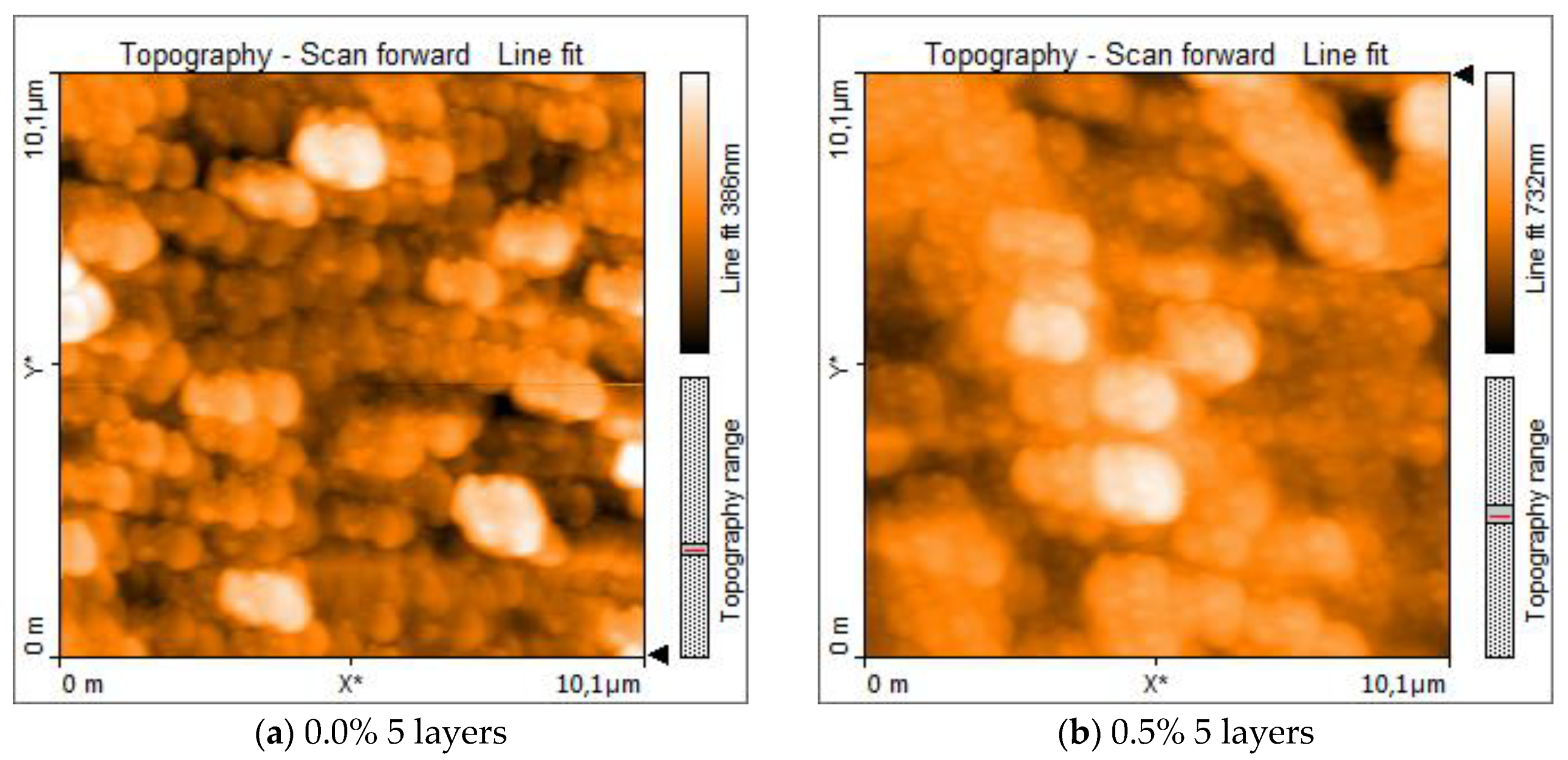
3.2. Surface Morphology

Images from AFM, Figure 2, were used to study the morphology for the 5- and 10-layered CuO films with various Sn doping concentrations.
The CuO thin film obtained with 10 layers exhibited a homogeneous porous structure with granules. The 5-layered film also exhibited a less uniform surface with agglomerates of a spherical shape. The surface roughness (Rms) decreased with increased dopant concentration. It varied from 83 to 49 nm for 5-layered films and from 64 to 41 nm for 10-layered films at 0–3 at% Sn content, as described in Table 1 and Table 2. Figure 2 also showed how the surface morphology was affected by the Sn doping concentration in both 5- and 10-layered films.

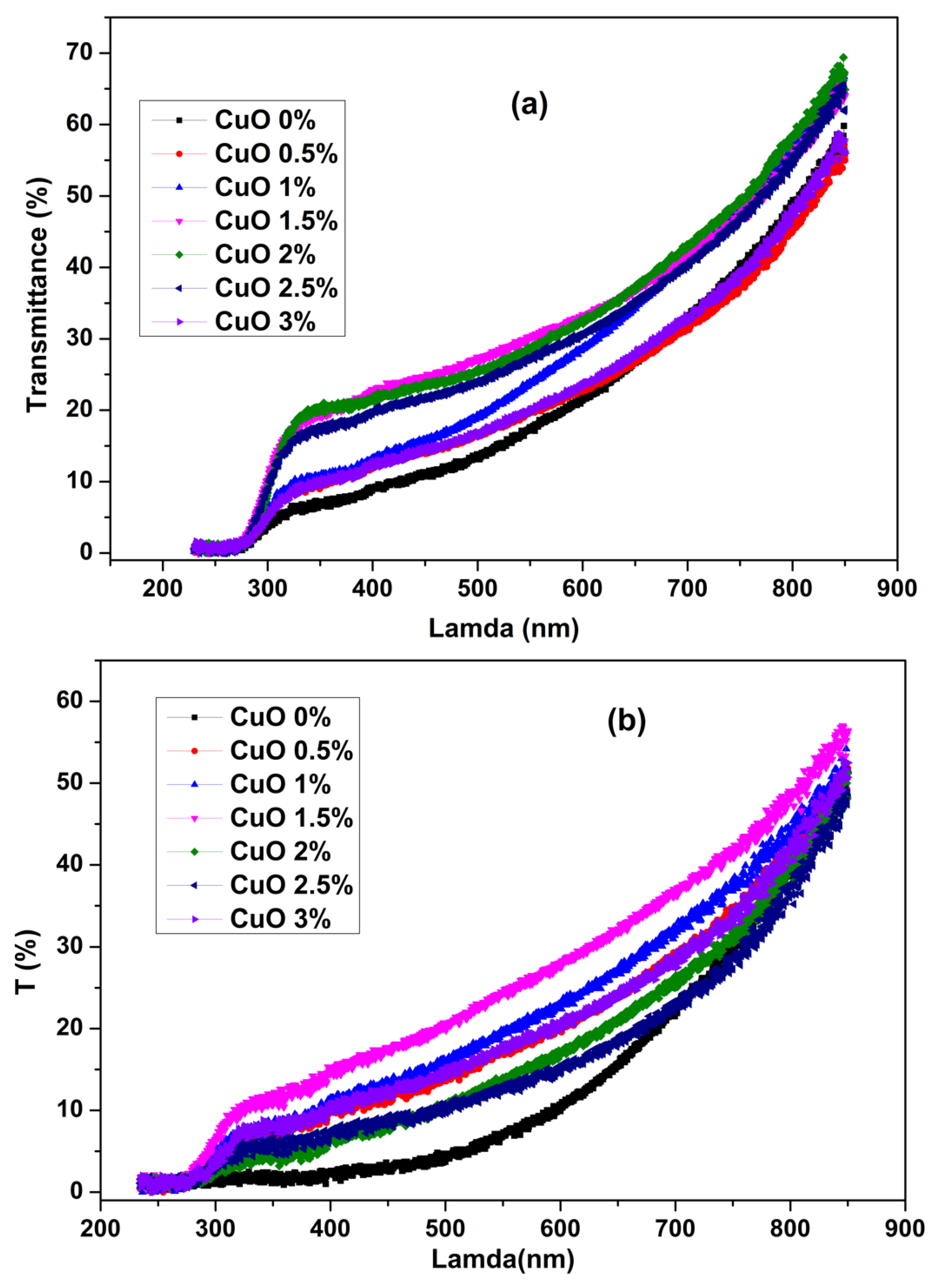
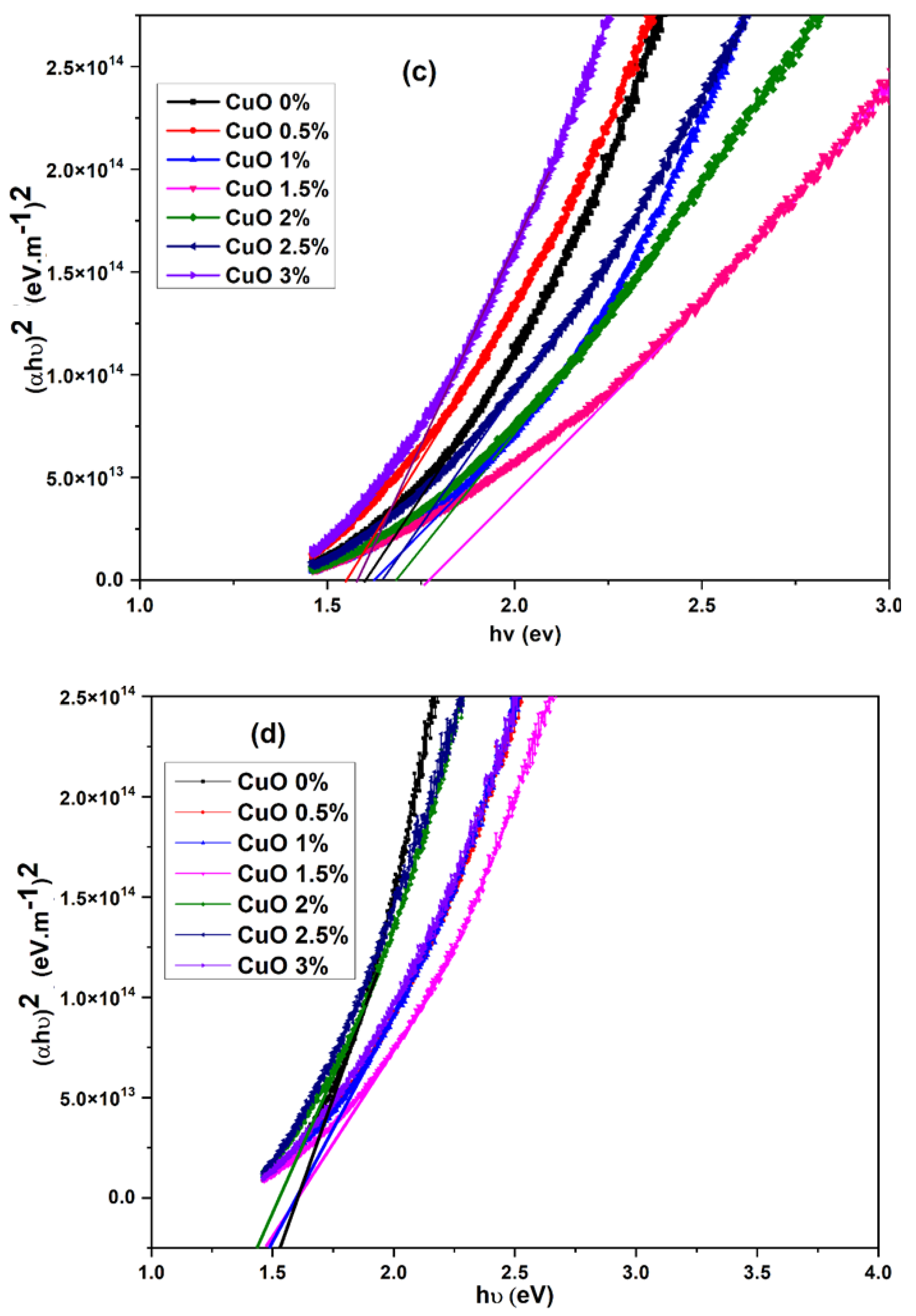
3.3. Optical Properties

Cu films, with 5 and 10 layers, having various Sn concentrations, were spectrophotometrically studied. Figure 3 shows the transmittance spectra (%) in the range of 250 to 800 nm. The Tauc plots are also shown in the Figure.
From the transmittance curves, Figure 3a,b, the films exhibited an average transmittance of 65% at waves longer than 800 nm. The abrupt drop in transmittance for waves shorter than 780 nm corresponded to the absorption in CuO due to electronic transitions between the valence band and the conduction band. At wavelengths 300 nm or lower, the transmittance values were close to 0. The results are consistent with earlier reports for pre-annealed CuO films [28].
In 5-layered films, the absorption thresholds of the doped layers at concentrations 1.5, 2.0, and 2.5 at% were shifted by ~60 nm in terms of wavelength compared to those doped at 0.0, 0.5, 1.0, and 3.0 at%. The presence of this offset indicates that the optical band gap value for CuO with doping 1.5, 2.0, and 2.5 at% is larger than that of CuO obtained at 0.0, 0.5, 1.0, and 3.0 at%.
Increasing the number of layers involves increasing the absorbance. This is understandable because more CuO layers involve more crystals and absorb more photons [1]. This is evidenced by the fact that the 10-layered films have higher overall film thickness than the 5-layered films, as shown in Table 1 and Table 2.
Eg values were calculated using the Tauc method, described in Equation (1), where the β optical constant describes the degree of disorder of the amorphous solid material. The absorption coefficient α can be calculated from the transmittance spectra of a layer using Equation (2) [29], which can be used to find film thickness.
The Tauc plots for the 5- and 10-layered films, with various Sn doping concentrations, are shown in Figure 3c,d, respectively. The optical gap values are presented in Table 1 and Table 2.
In 5-layered films with Sn doping of 1.5, 2.0, and 2.5 at%, the band gap value was larger than those for 0.0, 0.5, 1.0, and 3.0 at%. In 10-layered films, the increased Sn concentration continuously lowered the optical band gap value, except for the 3.0 at%, which exhibited a slight increase.
Under the doping effect, the observed optical changes could be due to many reasons, such as the formation of interstitial centers, the formation of defect complexes, or the appearance of a predominant phase where the oxide becomes stoichiometric [30].

3.4. Electrical Properties

The four-point probe method was used to study the electrical properties for 5- and 10-layered CuO films with various Sn doping concentrations. The current-voltage (I-V) curves sowed that all films exhibited an ohmic character, Figure 4.
The electrical resistivity was calculated using Equation (5):
ρ = R × k × e
where R□ is the Resistance per square, and k is a geometric factor that is equal to 4.53.
The results are shown in Figure 5. The Figure shows that the electrical conductivity varied by Sn dopant concentration in 5- and 10-layered CuO films. The electrical conductivity values are summarized in Table 1 and Table 2 for 5- and 10-layered CuO films, respectively.
In both 5- and 10-layered films, the conductivity varied significantly with Sn doping concentration. In both film types, as the Sn concentration was increased, the electrical conductivity increased up to a limit. In the case of the 5-layered film, the conductivity peak value occurred at doping concentration 2.0 at%, after which the films became less conductive than the 0.0 at%. In the 10-layered film, the conductivity peaked at 1.5 at% and decreased but still remained higher than that for the 0.0 at% film.
The increase in conductivity is understandable. By Sn doping, in the majority charge carriers, which are the holes, increase in the p-type CuO film. In doping, the Sn4+ ions substitute the Cu2+ in the CuO crystal lattices. The Sn4+ ion may then gain two electrons from the crystallite, which makes the latter p-type with more holes. Thus, each Sn4+ may potentially create two holes in the crystallite. With higher Sn concentration, more majority carriers (holes) are created, and consequently, the conductivity increases [24].
The optimal conductivities for 2.0 at% and 1.5 at% in 5- and 10-layered films are consistent with other film characteristics described above. From Table 1 and Table 2, these films exhibited the lowest thickness values among the series. The lower thickness values indicate higher densification compared to other films. Higher densification is one main reason for improved electrical conductivity, as described earlier for other types of films [31,32]. At Sn doping densities above these values, the film crystallite may involve higher imperfections which lower the conductivity. As stated in Section 3.1 above, the small lowering in crystallinity, with doping, was observed with small changes in the lattice parameters. This could be the reason for the conductivity lowering at higher Sn doping concentrations. In such a case, the crystallite imperfections balance off the dopant concentration effect.
Moreover, Figure 5 showed that the conductivity values for the 10-layered films were higher than their counterparts in the 5-layered films. This is understandable, because the four-point probe method only measured the film surface conductivity. Assuming that the two film types have same densification, then the 10-layered films with higher thickness must have higher conductivity that their 5-layered counterparts. Similar observations were reported for other types of thin film systems [33].
All in all, the results indicate that Sn doping affects the structural, morphological, optical, and, most significantly, electrical characteristics of CuO films prepared by sol–gel spin coating. The optimal conductivity, 50.3 × 10⁻³ (Ω·cm)−1, was observed for the 10-layered film with doping at 1.5 at%. This value is significantly higher than the earlier reported values for Sn-doped CuO films with conductivity values ranging from 21 × 10−3 to 12.9 × 10⁻³·(Ω·cm)−1 (resistivity ranging from 47.4 to 77.5 Ω·cm), albeit using higher Sn doping concentrations in 10-layered CuO films [24]. Collectively, the results encourage more study on these doped multi-layered CuO films. Co-doping, using safe elements, is another area to study. Varying the annealing temperature of the doped multi-layered CuO films is another proposed area.

4. Conclusions

Sn-doped CuO thin films were synthesized by the sol–gel method associated with spin coating. The films involved 5- and 10-layers, and doping concentration influenced the properties of both CuO films. X-ray diffraction patterns, measured for the 500 °C annealed films, showed that they involved the CuO pure phase. With increased dopant concentration, the electrical conductivity increased up to a limit in either type of layered films. Among various prepared systems, the 10-layered film with 1.5 at% Sn exhibited the lowest surface roughness and highest electrical conductivity. The results highlight the added value of doping CuO films with Sn to enhance their morphologies and electrical properties for future optoelectronic applications. A careful choice of doping concentration is necessary to yield optimal characteristics. The results also show that such a choice should be made depending on the number of CuO film layers.

Author Contributions

The work is based on N.A.A.’s thesis. The thesis was supervised by M.M. (Mustapha Mabrouki) and A.L., who both contributed to the ideas and design together with N.A.A. M.M. (Mohamed Manoua) and N.A.A. contributed with experimental work. N.A.A. and H.S.H. contributed with manuscript writing. H.S.H. contributed with correspondence and submission. All authors have read and agreed to the published version of the manuscript.

Funding

This research received no external funding.

Institutional Review Board Statement

Not applicable for studies not involving humans or animals.

Informed Consent Statement

Not applicable for studies not involving humans.

Data Availability Statement

The results are based on Naoual Al Armouzi’s Ph.D. Thesis. Data are available once needed.

Acknowledgments

The thrust of this work was conducted at Sultan Moulay Slimane University, Beni-Mellal-Morocco.

Conflicts of Interest

The authors declare no conflict of interest.

References

  1. Dahrul, M.; Alatas, H. Preparation and optical properties study of CuO thin film as applied solar cell on LAPAN-IPB Satellite. Procedia Environ. Sci. 2016, 33, 661–667. [Google Scholar] [CrossRef] [Green Version]
  2. Hussain, S.; Cao, C.; Nabi, G.; Khan, W.S.; Tahir, M.; Tanveer, M.; Aslam, I. Optical and electrical characterization of ZnO/CuO heterojunction solar cells. Optik 2017, 130, 372–377. [Google Scholar] [CrossRef]
  3. Abrahama, N.; Rufusc, A.; Philip, U.C.D. Dye sensitized solar cells using catalytically active CuO-ZnO nano-composite synthesized by single step method. Spectrochim. Acta Part A Mol. Biomol. Spectrosc. 2018, 200, 116–126. [Google Scholar] [CrossRef]
  4. Yang, B.; Liu, J.; Qin, H.; Liu, Q.; Jing, X.; Zhang, H.; Li, R.; Huang, G.; Wang, J. PtO 2 -nanoparticles functionalized CuO polyhedrons for n-butanol gas sensor application. Ceram. Int. 2018, 44, 10426–10432. [Google Scholar] [CrossRef]
  5. Singh, P.K.; Das, A.K.; Hatui, G.; Nayak, G.C. Shape controlled green synthesis of CuO nanoparticles through ultrasonic assisted electrochemical discharge process and its application for supercapaci-tor. Mater. Chem. Phys. 2017, 198, 16–34. [Google Scholar] [CrossRef]
  6. Kaur, G.; Saini, K.; Tripathi, A.K.; Jain, V.; Deva, D.; Lahiri, I. Room temperature growth and field emission characteristics of CuO nanostructures. Vacuum 2017, 139, 136–142. [Google Scholar] [CrossRef]
  7. Dolai, S.; Dey, R.; Das, S.; Hussain, S.; Bhar, R.; Pal, A.K. Cupric oxide (CuO) thin films prepared by reactive d.c. magnetron sputtering technique for photovoltaic application. J. Alloy. Compd. 2017, 724, 456–464. [Google Scholar] [CrossRef]
  8. Yuan, W.; Qiu, Z.; Chen, Y.; Zhao, B.; Liu, M.; Tang, Y. A binder-free composite anode composed of CuO nanosheets and multi-wall carbon nanotubes for high-performance lithium-ion batteries. Electrochim. Acta 2018, 267, 150–160. [Google Scholar] [CrossRef]
  9. Thi, T.V.; Rai, A.K.; Gim, J.; Kim, J. Potassium-doped copper oxide nanoparticles synthesized by asolvothermal method as an anode material for high-performance lithium ion secondary battery. Appl. Surf. Sci. 2014, 305, 617–625. [Google Scholar] [CrossRef]
  10. Wang, R.-C.; Lin, S.-N.; Liu, J.-Y. Li/Na-doped CuO nanowires and nanobelts: Enhanced electrical properties and gas detection at room temperature. J. Alloy. Compd. 2017, 696, 79–85. [Google Scholar] [CrossRef]
  11. Choi, Y.-H.; Kim, D.-H.; Hong, S.-H. p-Type aliovalent Li(I) or Fe(III)-doped CuO hollow spheres self-organized by cationic complex ink printing: Structural and gas sensing characteristics. Sens. Actuators B Chem. 2017, 243, 262–270. [Google Scholar] [CrossRef]
  12. He, M.; Wang, Y.; Wang, H.; Chen, R. A one-step sol–gel route derived Ag–CuO film as a novel solar selective absorber. Sol. Energy Mater. Sol. Cells 2016, 144, 264–272. [Google Scholar] [CrossRef]
  13. Ha, J.-W.; Oh, J.; Choi, H.; Ryu, H.; Lee, W.-J.; Bae, J.-S. Photoelectrochemical proper-ties of Ni-doped CuO nanorods grown using the modified chemical bath deposition method. J. Ind. Eng. Chem. 2017, 25, 38–44. [Google Scholar]
  14. Abdel-Galil, A.; Moussa, N.L.; Yahia, I.S. Study on spray deposited Ni-doped CuO nanostructured thin films: Micro-structural and optical behavior. J. Mater. Sci. Mater. Electron. 2022, 33, 4984–4999. [Google Scholar] [CrossRef]
  15. Bosigo, R.; Lepodise, L.M.; Chimowa, G.; Muiva, C. Enhanced ethanol sensing response of nanostructured Ce-doped CuO thin films. Mater. Chem. Phys. 2022, 280, 125841. [Google Scholar] [CrossRef]
  16. Rahaman, R.; Sharmin, M.; Podder, J. Band gap tuning and p to n-type transition in Mn-doped CuO nanostructured thin films. J. Semicond. 2022, 43, 012801. [Google Scholar] [CrossRef]
  17. Ruzgar, S.; Caglar, Y.; Polat, O.; Sobola, D.; Caglar, M. Tuning the optical and morphological features of CuxO thin films via La doping. Phys. B: Condens. Matter 2021, 615, 413088. [Google Scholar] [CrossRef]
  18. Wang, Y.; Jiang, T.; Meng, D.; Yang, J.; Li, Y.; Ma, Q.; Han, J. Fabrication of nanostructured CuO films by electrodeposition and their photocatalytic properties. Appl. Surf. Sci. 2014, 317, 414–421. [Google Scholar] [CrossRef]
  19. Mohebbi, S.; Molaei, S.; Azar, A.R.J. Preparation and study of Sn-doped CuO nanoparticles as semiconductor. J. Appl. Chem. 2013, 8, 27. [Google Scholar]
  20. Aadim, K.A.; Ahmed, B.M.; Khalaf, M.A. Influence of Sn doping ratio on the structural and optical properties of CdO films prepared by laser induced plasma. Iraqi J. Phys. 2020, 18, 1–8. [Google Scholar] [CrossRef]
  21. Eisermann, S.; Kronenberger, A.; Laufer, A.; Bieber, J.; Haas, G.; Lautenschläger, S.; Homm, G.; Klar, P.J.; Meyer, B.K. Copper oxide thin films by chemical vapor deposition: Synthesis, characterization and electrical properties. Phys. Status Solidi A 2011, 209, 531–536. [Google Scholar] [CrossRef]
  22. Czerwosz, E.; Wronka, H.; Kozłowski, M.; Diduszko, R.; Kęczkowska, J.; Suchańska, M. Preparation of n-CuO nanostructural films by thermal oxidation/PVD method. In Photonics Applications in Astronomy, Communications, Industry, and High-Energy Physics Experiments; SPIE: Bellingham, WA, USA, 2019. [Google Scholar]
  23. Parvathy, T.; Sabeer, N.A.M.; Mohan, N.; Pradyumnan, P.P. Effect of dopant gas pressure on the growth of magnetron sputtered CuO thin films for electrical and optical applications. Opt. Mater. 2022, 125, 112031. [Google Scholar] [CrossRef]
  24. Wu, J.; Hui, K.S.; Li, L.; Chun, H.-H.; Cho, Y.R. Characterization of Sn-doped CuO thin films prepared by a sol–gel method. J. Mater. Sci. Mater. Electron. 2015, 27, 1719–1724. [Google Scholar] [CrossRef]
  25. Sert, E.; Sayrac, M. Investigation of optical and structural properties of tin-doped copper oxide thin films prepared by the drop cast method. J. Aust. Ceram. Soc. 2022, 58, 93–100. [Google Scholar]
  26. Animasahun, L.O.; Taleatu, B.A.; Adewinbi, S.A.; Bolarinwa, H.S.; Fasasi, A.Y. Synthesis of SnO2/CuO/SnO2 Multi-layered Structure for Photoabsorption: Compositional and Some Interfacial Structural Studies. J. Niger. Soc. Phys. Sci. 2021, 3, 74–81. [Google Scholar] [CrossRef]
  27. Al Armouzi, N.; El Hallani, G.; Liba, A.; Zekraoui, M.; Hilal, H.S.; Kouider, N.; Mabrouki, M. Effect of annealing temperature on physical characteristics of CuO films deposited by sol-gel spin coating. Mater. Res. Express 2019, 6, 116405. [Google Scholar] [CrossRef]
  28. Lee, W.-J.; Wang, X.-J. Structural, Optical, and Electrical Properties of Copper Oxide Films Grown by the SILAR Method with Post-Annealing. Coatings 2021, 11, 864. [Google Scholar] [CrossRef]
  29. Al Armouzi, N.; Manoua, M.; El Hallani, G.; Hilal, H.S.; Liba, A.; Kouider, N.; Mabrouki, M. Effects of Sn Doping on Properties of Multilayered ZnO Films Deposited by Spin Coating/Sol–Gel Method. JOM 2020, 73, 411–419. [Google Scholar] [CrossRef]
  30. Neskovska, R.; Ristova, M.; Velevska, J. Electrochromism of the electroless deposited cuprous oxide films. Thin Solid Film. 2007, 515, 4717–4721. [Google Scholar] [CrossRef]
  31. Han, W.; Kim, J.; Park, H.-H. Control of electrical conductivity of highly stacked zinc oxide nanocrystals by ultraviolet treatment. Sci. Rep. 2019, 9, 6244. [Google Scholar] [CrossRef]
  32. Nian, Q.; Callahan, M.; Look, D.; Efstathiadis, H.; Bailey, J.; Cheng, G.J. Highly transparent conductive electrode with ultra-low HAZE by grain boundary modification of aqueous solution fabricated alumina-doped zinc oxide nanocrystals. APL Mater. 2015, 3, 062803. [Google Scholar] [CrossRef] [Green Version]
  33. Lin, Q.; Zhang, F.; Zhao, N.; Yang, P. Influence of Annealing Temperature on Optical Properties of Sandwiched ZnO/Metal/ZnO Transparent Conductive Thin Films. Micromachines 2022, 13, 296. [Google Scholar] [CrossRef] [PubMed]
Figure 1. XRD patterns measured for CuO thin films with various Sn doping concentrations. (a) 5- and (b) 10-layered.
Processes 10 01277 g001
Figure 2. AFM images measured for 5- and 10-layered CuO thin films with various Sn doping concentrations. X* and y* refer to scale.
Processes 10 01277 g002aProcesses 10 01277 g002bProcesses 10 01277 g002c
Figure 3. Optical properties for CuO films with various Sn concentrations. Optical transmittance spectra are shown in (a) for 5 layers, and (b) for 10 layers. Tauc plots (αhν)2 versus hν are shown in (c) for 5 layers and in (d) for 10 layers.
Processes 10 01277 g003aProcesses 10 01277 g003b
Figure 4. I-V characteristic measurements of CuO films for various Sn content: (a) 5 layers and (b) 10 layers.
Processes 10 01277 g004aProcesses 10 01277 g004b
Figure 5. Measured conductivity values for 5- and 10-layered CuO films with various Sn concentrations.
Processes 10 01277 g005aProcesses 10 01277 g005b
Table 1. The crystallite size (D), the lattice parameter c, the conductivity (σ), the thickness (e), the root mean square (RMS), and the band gap (Eg) of CuO thin films with 5 layers at various doping concentrations.
Doping Concentration (at%)Crystallite Size (nm)c (Ǻ)Thickness (nm)σ (Ω·cm)−1·10−3RMS (nm)Eg (eV)
035.35.026275.08.2831.60
0.537.95.050244.611781.55
129.75.022278.617721.63
1.535.35.034281.422661.77
230.35.027247.345491.69
2.530.35.045234.27.4561.65
336.35.046218.56.8621.58
Table 2. The crystallite size (D), the lattice parameter c, the conductivity (σ), the thickness (e), the root mean square (RMS), and the band gap (Eg) of CuO thin films with 10 layers at various doping concentrations.
Doping ConcentrationCrystallites Size (nm)c (Ǻ)Film Thickness (nm)σ (Ω·cm)−1·10−3RMS (nm)Optical Band Gap Eg (eV)
0%29.15.032340.212.2501.54
0.5%34.85.036320.622.0461.50
1.0%35.05.031295.331.7441.49
1.5%35.05.028283.650.3411.47
2.0%35.55.036290.427.5561.43
2.5%35.95.029301.026.7591.41
3.0%36.95.030310.025.2641.49
Publisher’s Note: MDPI stays neutral with regard to jurisdictional claims in published maps and institutional affiliations.

