1. Introduction
Microwave plasma chemical vapor deposition (MPCVD) is an emerging technology commonly used in the preparation of crystalline materials [
1] and has broad application prospects in the preparation of high-quality carbon material and tool coatings [
2,
3,
4]. The MPCVD process is complex and includes a variety of physical and chemical processes that vary greatly in both temporal and spatial scales. Compared with other CVD processes, MPCVD has significant advantages in synthesizing large-area diamond films [
5] and has a wider range of applicable parameters, which provides the possibility for applications in various situations [
6]. It can achieve low-temperature growth [
7], carbon nanotube alignment growth, and structural control [
8]. In depositing the carbon material with the MPCVD apparatus, a DC bias voltage can be applied between the substrate and the deposition chamber to superimpose the electrical and electromagnetic excitations.
Stöckel et al. [
9,
10] explored the effect of positive bias pretreatment in the MPCVD system on the growth of diamonds on the Si surface through experiments. They found that the DC and plasma shapes changed during the bias pretreatment process, as did the deposition density on the substrate, its chemical and crystalline properties, and the nucleation density of subsequent diamond growth. Based on this, a relatively complete bias model is proposed. Chiang et al. [
11] found that applying positive substrate bias also enhanced diamond nucleation on the surface of smooth Si substrates. The nucleation density could be increased to 10
10 cm
−2, generating more uniformly textured diamond films at lower microwave power and deposition pressure. The positive bias-enhanced CVD process has greater advantages in preparing high-quality diamond films.
Thus far, there are very few numerical simulation studies on the bias-enhanced MPCVD process in the literature, and most are experimental studies on the process, which mainly focus on the process parameters affecting the surface quality and growth rate of the deposited carbon materials. However, studies on how the positive bias voltage affects the plasma flow characteristics in the deposition chamber are rare.
The numerical model of the MPCVD process was first established by German scientists Füner et al. [
12,
13], who developed a computational model for simulating the electromagnetic field and plasma density distribution in the MPCVD reaction chamber. Japanese scholars Yamada et al. [
14,
15] proposed a calculation method based on a fluid model that calculated parameters such as the electromagnetic field distribution and electron number density in the deposition cavity by coupling Maxwell’s equations and the fluid conservation equation of electrons. The energy conservation equation of the electron temperature distribution is obtained. Then, Yamada et al. [
16,
17] introduced the gas composition based on the plasma model and first calculated the power density of the plasma according to the coupling of the electron transport equation and Maxwell’s equation, then used this as the heat source term to solve the governing equation of the gas species distribution. This method has since been optimized to simulate the more complex CH4 discharge reaction mechanism [
18] and other gas components (Ar [
19] and N2 [
16]).
In this paper, plasma is regarded as a special fluid, and by studying its macroscopic performance, it has a certain guiding significance for the parameter control of practical engineering applications.
‘Plasma flow characteristics’ are the plasma macroscopic flow field properties defined by imitating the general fluid. The change of the flow field in the deposition chamber is observed by increasing the bias strength to provide a reference for engineering applications, so the difference between electron flow and ion flow is not specifically shown. This paper uses the multiphysics simulation software COMSOL Multiphysics 6.0 to establish a two-dimensional axisymmetric plasma model of pure H2 discharge. Version 6.0 of the COMSOL Multiphysics® software is released by COMSOL in Sweden. According to the established multiphysics coupling model, the influence of different positive bias intensities on the plasma flow characteristics in the deposition chamber is calculated. The influence of the intensity change of positive bias voltage and deposition pressure on plasma flow characteristics was explored, and its mechanism of action in the chemical vapor deposition process was analyzed.
2. Materials and Methods
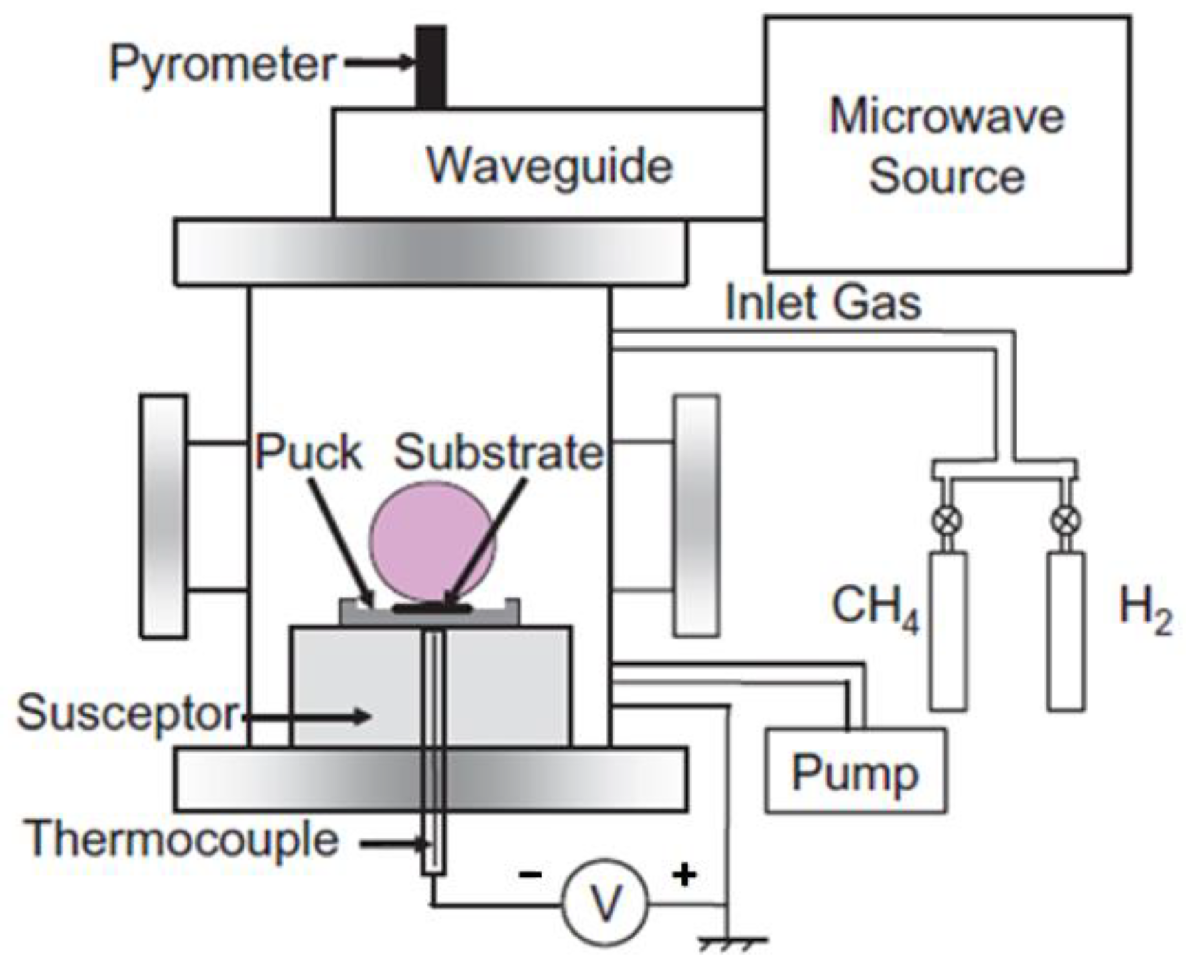
The MPCVD equipment model studied in this paper is the SEKI AX5200S made in Seki Technotron Corp. from Japan, which belongs to the quartz plate microwave plasma resonator type. It is often used to prepare diamond films. The microwave source provides a 2.45 GHz microwave, and the volume fraction of H
2 in the input gas is generally above 90%. The schematic diagram of the specific device is shown in
Figure 1.
In solving the model, it is necessary first to calculate the electric field distribution, then calculate the electromagnetic field, that is, to solve Maxwell’s equations. Equation (1) can be obtained by solving Maxwell’s equations:
where,
w is the angular frequency of the electromagnetic wave,
and
are the relative permittivity and relative permeability, respectively.
Plasma is equivalent to a dielectric in the electromagnetic field, so its conductivity and permittivity should be considered when calculating the electromagnetic field distribution, both of which can be represented by the following equations [
21]:
where,
and
are the plasma’s angular and effective collision frequencies, respectively.
The plasma is calculated by the method of drift-diffusion approximation. In the solution process, the shape of the plasma is assumed to be stable, and the following formula provides its governing equation:
where,
Rn is the particle number variable in the collision process,
Rd is the particle momentum variable in the collision process,
Rε is the energy density variable in the collision process,
n is the particle number density,
represents the average velocity of the particle, and
is the heat flux vector.
The electron collision reaction rate is calculated from the collision cross-section:
where,
is the reaction rate of the electron production and consumption,
is the square root of twice the electron charge mass ratio, σ is the electron impact cross section,
f is the electron energy distribution function,
is the mass fraction of the ith component,
Nn is the number density of heavy particles,
ne is the number density of electrons.
In calculating the heat transfer model, the convection effect can be ignored due to the low gas flow in the deposition chamber. The governing equation for the heat transfer model calculation is:
where,
k is the thermal conductivity of the gas;
Qgas is the heat source term due to the collision between electrons and neutral gas molecules;
δ is the energy loss coefficient of the collision between electrons and neutral gas molecules;
kB is the Boltzmann constant.
Mesh generation is a key step in model calculation. A proper mesh generation method can consider both computational efficiency and accuracy. The mesh generation function of the COMSOL Multiphysics 6.0 software is used. Considering the simulation complexity, different mesh precisions are selected for different calculation domains. The upper part of the calculation domain is only used for simple electromagnetic field calculations, so the region meshes with coarse elements. The region contains 490 mesh elements with a minimum mass of 0.5561 and an average of 0.8108. The lower part of the computational domain needs more sophisticated multi-physical field coupling calculations, so more refined mesh settings are required. The figure of meshing can be seen in
Figure 2.
The relationship between the bias current and the intensity on the substrate surface was selected to verify the rationality and credibility of the physics coupling model. The results are shown in
Figure 3.
In the process of synthesizing diamond by MPCVD equipment, Barrat [
22] measured the variation of the bias current on the substrate surface with the negative bias intensity of the substrate when the pressure was 10 torr, and the microwave power was 600 W, as shown in the blue curve in the figure shown. The qualitative law shown by the curve formed by the data is consistent. As the bias strength increases, the bias current also increases. Although there are numerical errors, they are enough to prove the rationality and credibility of the multiphysics coupling model.
3. Results
3.1. Effect of Positive Bias on Plasma Flow Characteristics
When a positive bias is applied to the substrate, the increased bias strength will influence the plasma flow characteristics.
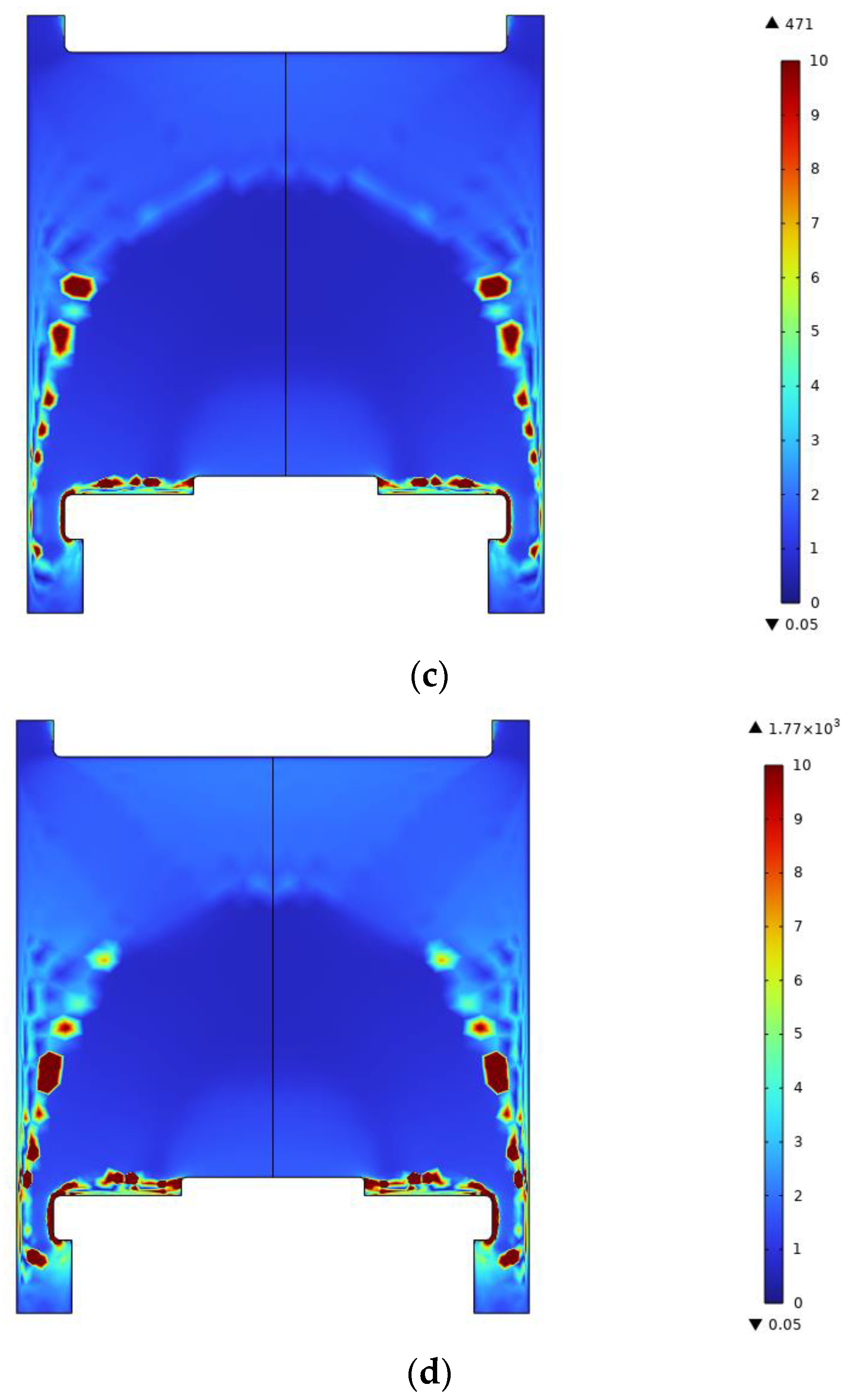
Figure 4 shows the contours of the velocity distribution in the deposition chamber under four working conditions. The contours under the four working conditions of 0, +100, +200, and +300 V were compared and analyzed. In this simulation, the deposition pressure is 10 torr, and the microwave power is selected at 600 W.
Under the condition that the deposition pressure remains unchanged, the distribution of the velocity field in the chamber does not change greatly when the strength of the positive bias is changed. However, the maximum velocity value in the chamber increases with bias strength. When the bias voltage changes from 0 to +100 V, the maximum speed increases by 1.55%. When the bias voltage changes from +100 to +200 V, the maximum speed increases by 1.36%, and when the bias voltage is changed from +200 V to +300 V, the maximum speed increases by 2.52%. By analyzing and comparing the above data, when the bias voltage is in the range of +100 V to +200 V, the increase in the maximum flow velocity in the chamber is relatively slow. As the positive bias strength continues to increase, the magnitude of the increase in flow velocity within the chamber is enhanced.
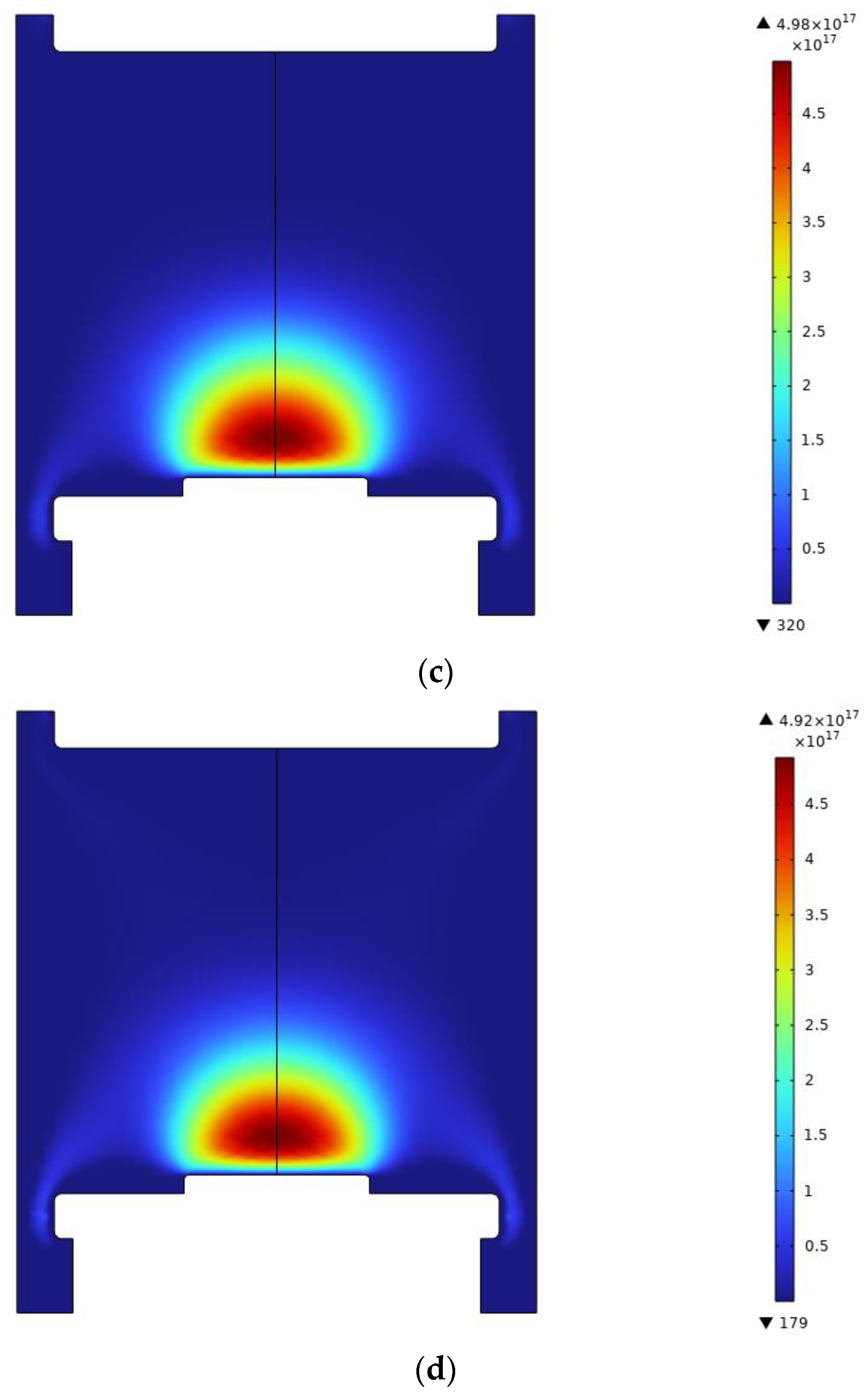
Figure 5 shows the contour plots of the electron temperature distribution under four different working conditions. Under the positive bias of the substrate, the narrow thermal region of the electron temperature disappears, and the high-temperature region of the electron temperature is dispersed into the deposition chamber and shows a very chaotic point-like distribution. Although it is seemingly irregular, the high-temperature regions are mainly concentrated on the sidewall of the reactor and the surface of the substrate table below the substrate, that is, the grounded surface. It is because when the substrate is in a positive bias state, the ground surface instead has a relatively low potential. As a result, an ion sheath forms on the ground surface, creating a region of high electron temperature. Under positive bias, electrons and ions move in different directions. Due to the difference between the properties of electrons and ions, the surrounding electric field has changed greatly, so the phenomenon of abnormally high field strength occurs. It is a kind of edge effect.
The electron temperature in the deposition cavity shows this distribution because the substrate bias voltage generates a high field strength area through the edge effect (shown in
Figure 6) and then transfers the energy to the electrons near the surface. Moreover, because the electron density in the peripheral area of the deposition cavity is low, the collision effect is weakened, the electron energy loss is reduced, and the energy carried by free electrons is increased. The macroscopic performance is that the electron temperature is increased. However, this distribution of high-energy free electrons will cause most of the input energy to be dissipated on the reactor wall. It cannot be transferred to neutral particles or positive ions, thus affecting the deposition process and energy utilization rate.
In addition, the electron density distribution shown in
Figure 7 can more intuitively observe the flow direction of particles in the deposition chamber during the deposition process.
Figure 8 shows the variation law of the axial electron average temperature in the deposition chamber with the bias strength of the substrate. The changing trend of electron temperature is consistent, which generally decreases first and then increases. The electron temperature is relatively stable in the central area of the substrate and gradually increases in the edge area of the substrate. Applying a positive bias voltage will make the distribution of high-energy free electrons in the deposition chamber more dispersed, thereby affecting the plasma flow characteristics in the chamber.
3.2. Effect of Deposition Pressure on Plasma Flow Characteristics
The collision process shown in
Table 1 is considered. Although it is a rather simplified
discharge mechanism, which includes the main reactions that generate H atoms,
ions and excited
.
The calculation conditions selected in this paper are 10, 30, 50, and 70 torr. In the simulation, the bias voltage is 0 V, and the microwave power is selected at 600 W. The first three reactions in
Table 1 are mainly considered when analyzing the influence of air pressure.
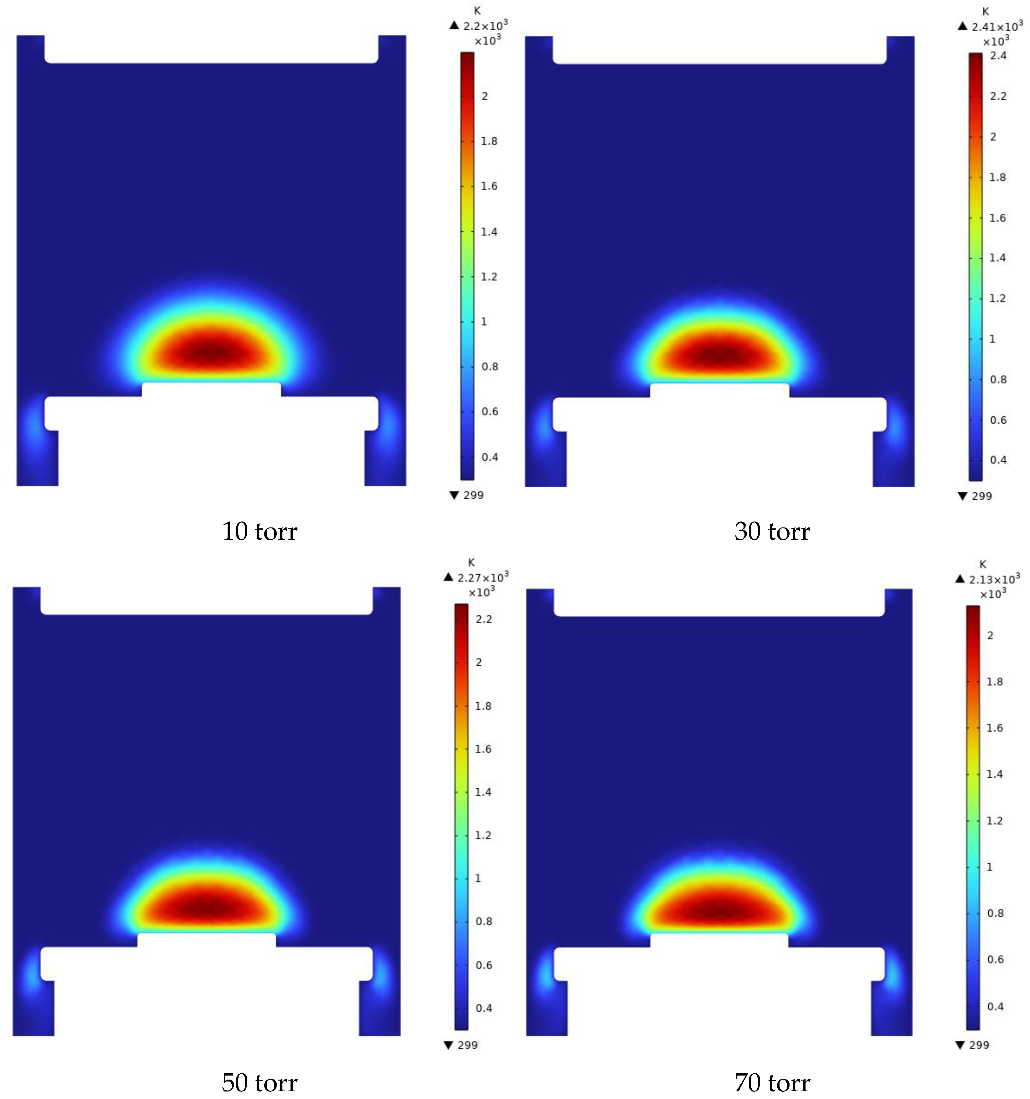
The variation of the velocity distribution inside the deposition chamber is shown in
Figure 9. A relatively obvious hemispherical velocity field is formed above the substrate with the increase in deposition pressure. At the same time, the velocity change at the exit of the chamber gradually becomes gentle. When the deposition pressure changed from 10 to 30 torr, the maximum flow velocity in the chamber decreased by 27.72%. When the deposition pressure changed from 30 to 50 torr, the maximum flow velocity in the chamber decreased by 8.99%. When the deposition pressure changed from 50 to 70 torr, the maximum flow velocity in the chamber decreased by 2.33%. By analyzing and comparing the above data, the increase in the deposition pressure decreases the maximum flow velocity in the chamber. With the increase in deposition pressure, the velocity field at the place where the plasma ball is formed above the substrate changes obviously. Therefore, it is speculated that the increase in the deposition pressure has a certain enhancement effect on the plasma flow.
The variation in the temperature distribution inside the deposition chamber is shown in
Figure 10. With the increase in deposition pressure, the temperature field above the substrate gradually becomes flat, and the center of the plasma ball is the maximum temperature. When the deposition pressure changed from 10 to 30 torr, the maximum temperature in the chamber increased by 9.55%. When the deposition pressure changed from 30 to 50 torr, the maximum temperature in the chamber decreased by 5.81%. When the deposition pressure changed from 50 to 70 torr, the maximum temperature in the chamber decreased by 6.17%. By analyzing and comparing the data above, the maximum temperature value in the chamber first increases and then decreases with the increase in deposition pressure. From the change in the temperature field distribution in the cloud map, the increase in deposition pressure gradually shrinks the high-temperature area in the chamber. The temperature at the center of the plasma ball will reach a maximum when the deposition pressure is approximately 30 torr.
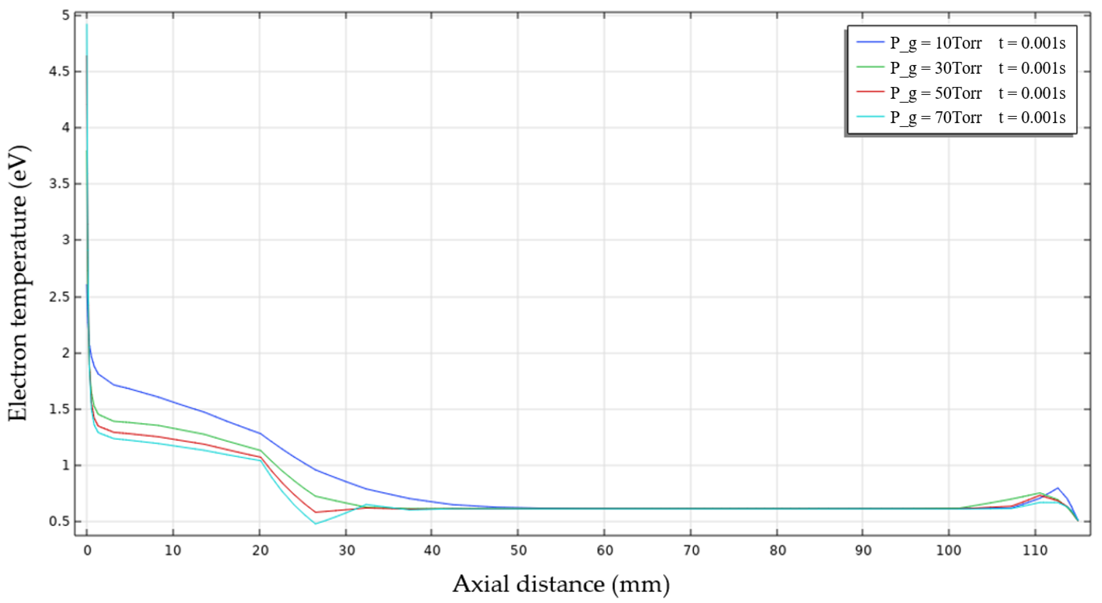
The rear part of the curves in
Figure 11 shows the opposite trend compared to the front. With increasing pressure, the electron temperature of the substrate increases too. Although the pressure causes the collision effect to increase, the electron density also decreases simultaneously. The probability of collision between the electron and other particles decreases, causing a small increase in the electron temperature, which then affects the temperature field distribution in the chamber.
4. Discussion
Under the positive bias of the substrate, the narrow thermal region of the electron temperature disappears, and the high-temperature region of the electron temperature is dispersed into the deposition chamber and presents a very chaotic point-like distribution. Although it seems irregular, the high-temperature regions are mainly concentrated on the side walls of the reactor and the surface of the substrate table below the substrate, that is, the grounded surface. It is because when the substrate is in a forward-biased state, the ground surface instead has a relatively low potential, so an ion sheath is formed on the ground surface, resulting in a region of high electron temperature.
With the increase in bias intensity, the increase rate of the average electron temperature in the deposition chamber decreases, while the increase rate of the maximum electron temperature increases and decreases. The result is opposite to that in the case of negative bias. The distribution of high-energy free electrons in the deposition chamber tends to be more dispersed, adversely affecting the deposition process.
The pressure affects the plasma characteristics within the deposition chamber by changing the mean free path between electrons and other particles. Under low-pressure conditions, the free travel of electrons is greater, the collision probability is lower, and the plasma volume is larger.
With the increase in deposition pressure, the free path of electrons decreases, the collision effect increases, the electron density also decreases, and the decrease in electron density reduces the collision probability. Therefore, the negative correlation between electron density and collision probability results in a small increase in the plasma deposition area under high-pressure conditions.
5. Conclusions
In summary, under the positive bias condition, it can be found that when the bias voltage is in the range of +100 V to +200 V, the increase in the maximum flow velocity in the chamber is relatively slow. As the positive bias strength continues to increase, the magnitude of the increase in flow velocity within the chamber is enhanced. Applying a positive bias voltage will make the distribution of high-energy free electrons in the deposition chamber more dispersed, thereby affecting the particle motion in the chamber.
When the microwave power remains unchanged and the deposition pressure changes, the effect on the plasma properties in the deposition chamber is achieved by changing the mean free path between electrons and other particles. With the increase in pressure, the electron temperature in the deposition chamber increases locally and reaches the maximum value of approximately 30 torrs. It is the decrease in electron density and the increase in collision probability occurring simultaneously owing to the change in pressure.


