
Modern Physical-Mathematical Models and Methods for Design Surface Acoustic Wave Devices: COM Based P-Matrices and FEM in COMSOL

Abstract
:1. Introduction
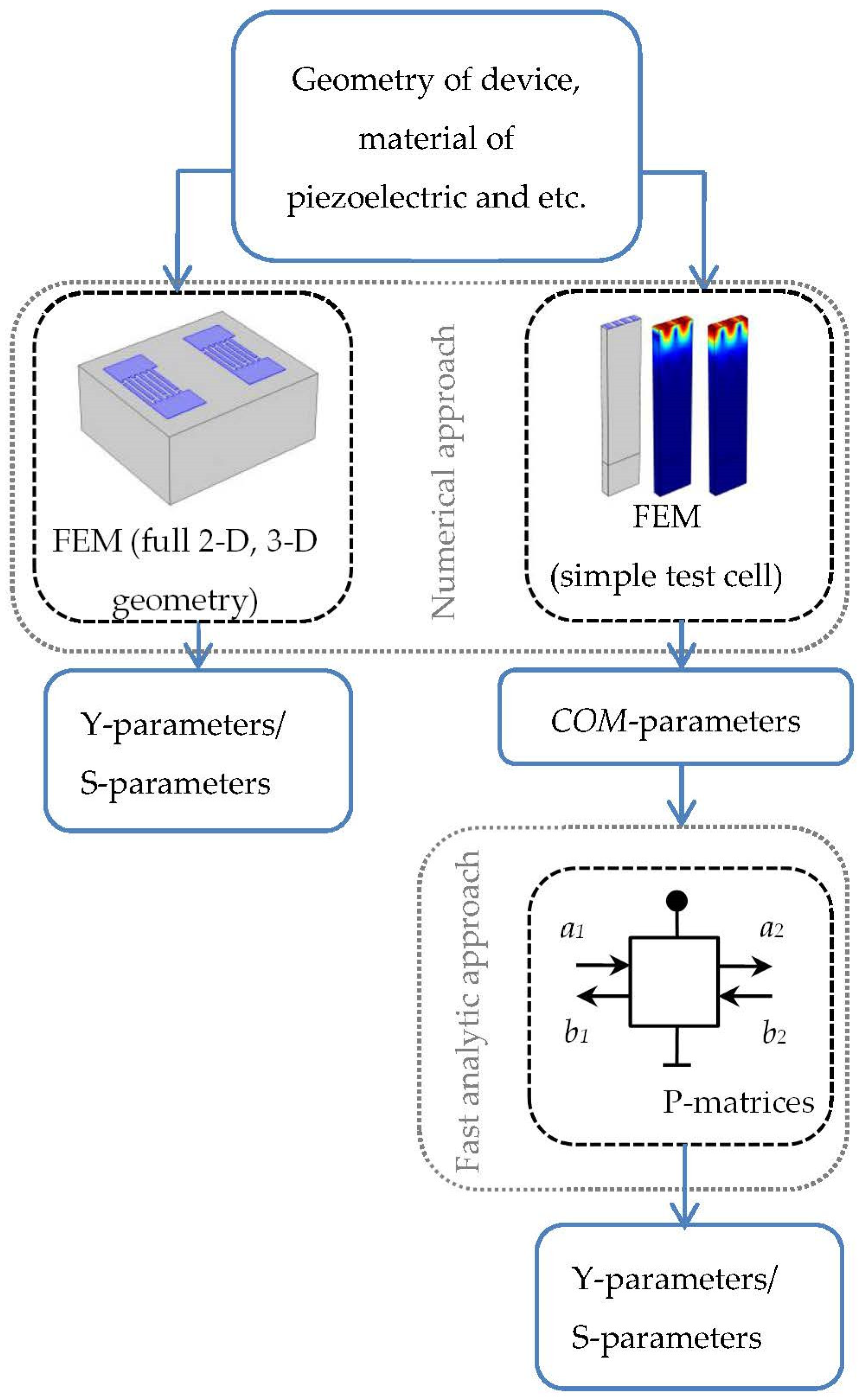
2. Physical-Mathematical Models
2.1. COM-Model
- 1.
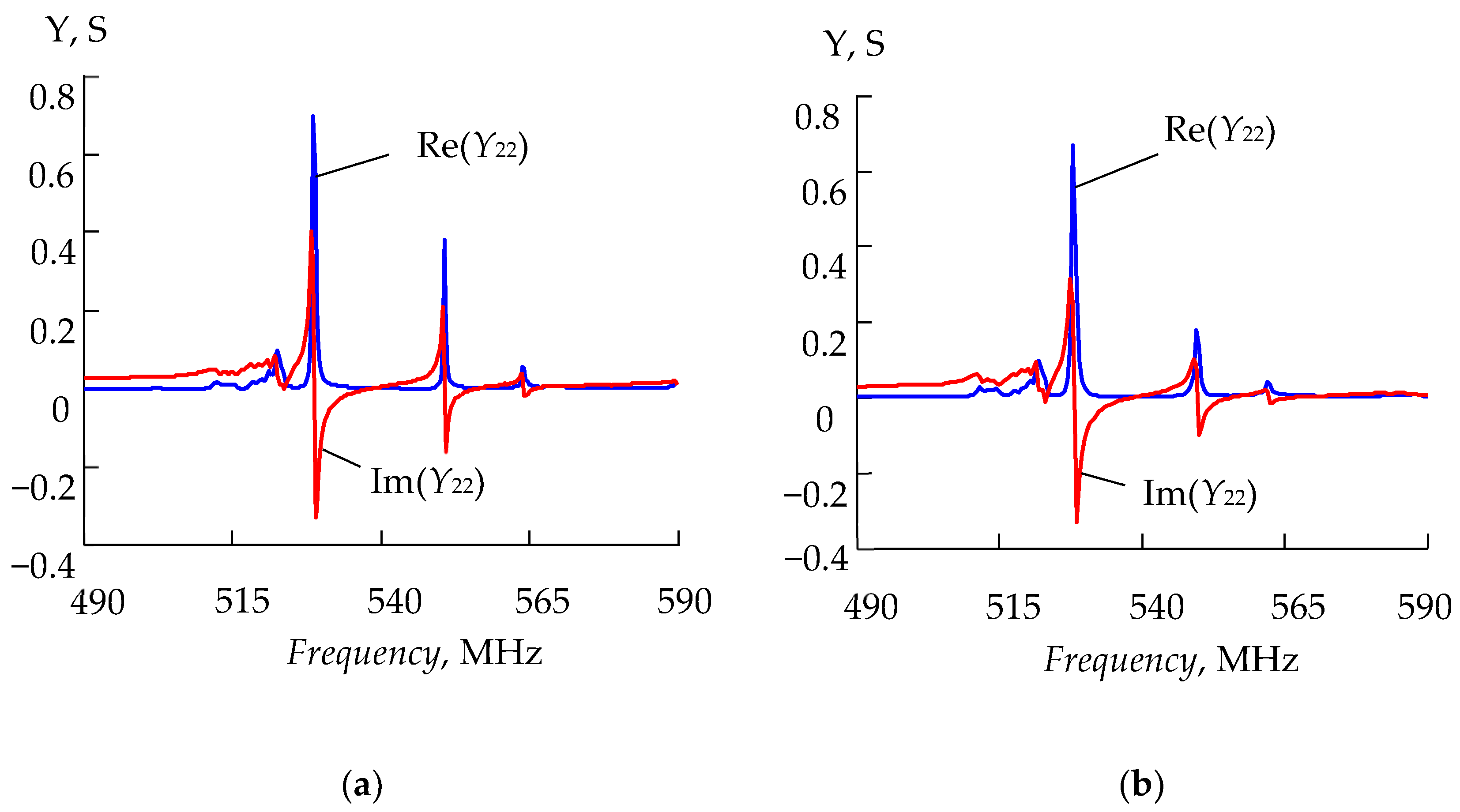
- The physical interpretation of all components of the P-matrices [9,10]. Acoustic components P11, P12, P21, and P22 describe the transmission and reflection coefficients over the acoustic ports. The components P13 and P23 show the efficiency of excitation of surface acoustic waves by applying voltage U to the bus bars of the IDT. The components P31 and P32 characterize the efficiency of conversion of SAW into the electric current I in the IDT. P13, P23, P31, and P32 are directly proportional to the effective value of the electromechanical coupling coefficient. The element P33 of the total matrix determines the desired admittance of the device. To analyze the devices, it is necessary to determine all the components of the P-matrices;
- 2.
- Rules for cascading P-matrices [9]. So, for example, the element P33 of the total P-matrix of two “neighboring” blocks is calculated by the formula:
- 3.
- The transition from a set of Y-parameters to S-parameters. Example of recalculation for the transmission coefficient:
- 4.
- Analytical solutions;
- Extraction of parameters from experimental data with subsequent construction of empirical dependencies;
- Numerical solutions based on FEM.
2.2. FEM in COMSOL
- (1)
- The transducer must have no apodization by amplitude weighting;
- (2)
- The transducer aperture must not be less than 15 wavelengths; otherwise, the waveguide effect must be taken into account [28];
- (3)
- The distance between neighboring transducers should be small, then it is possible not to take diffraction into account;
- (4)
- The solution for a small aperture extends to the full transducer aperture with the accuracy of the aperture coefficient;
- (5)
- We do not consider the influence of contact bus bars.
- Defining the workspace and setting the geometry;
- The input of initial data (material, aperture, etc.);
- Setting the initial and boundary conditions (potentials on the electrodes, a perfectly matched layer (PML), etc.);
- Building a mesh;
- Determination of the parameters of the solver and calculation.
3. Results
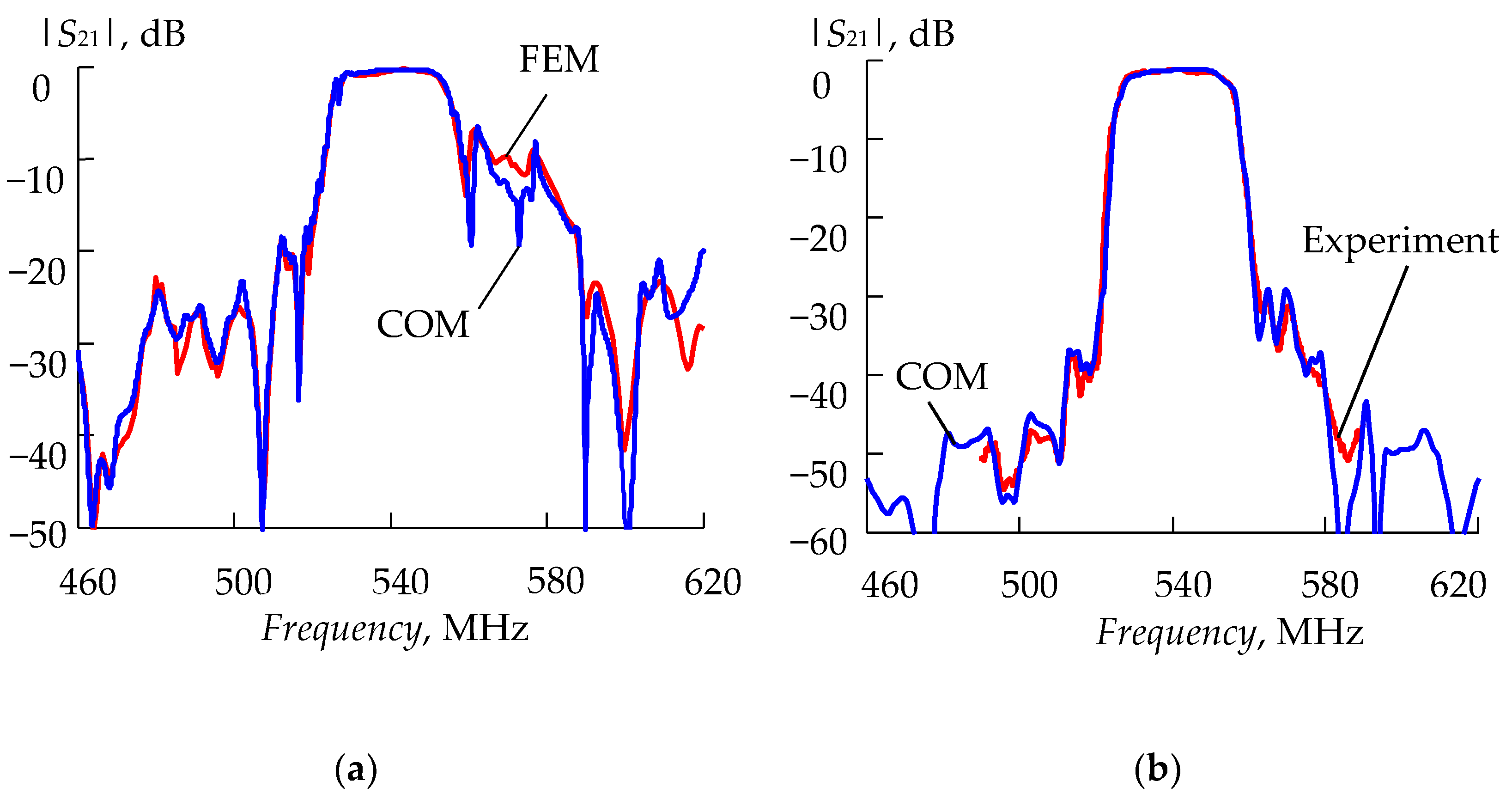
3.1. DMS Filter
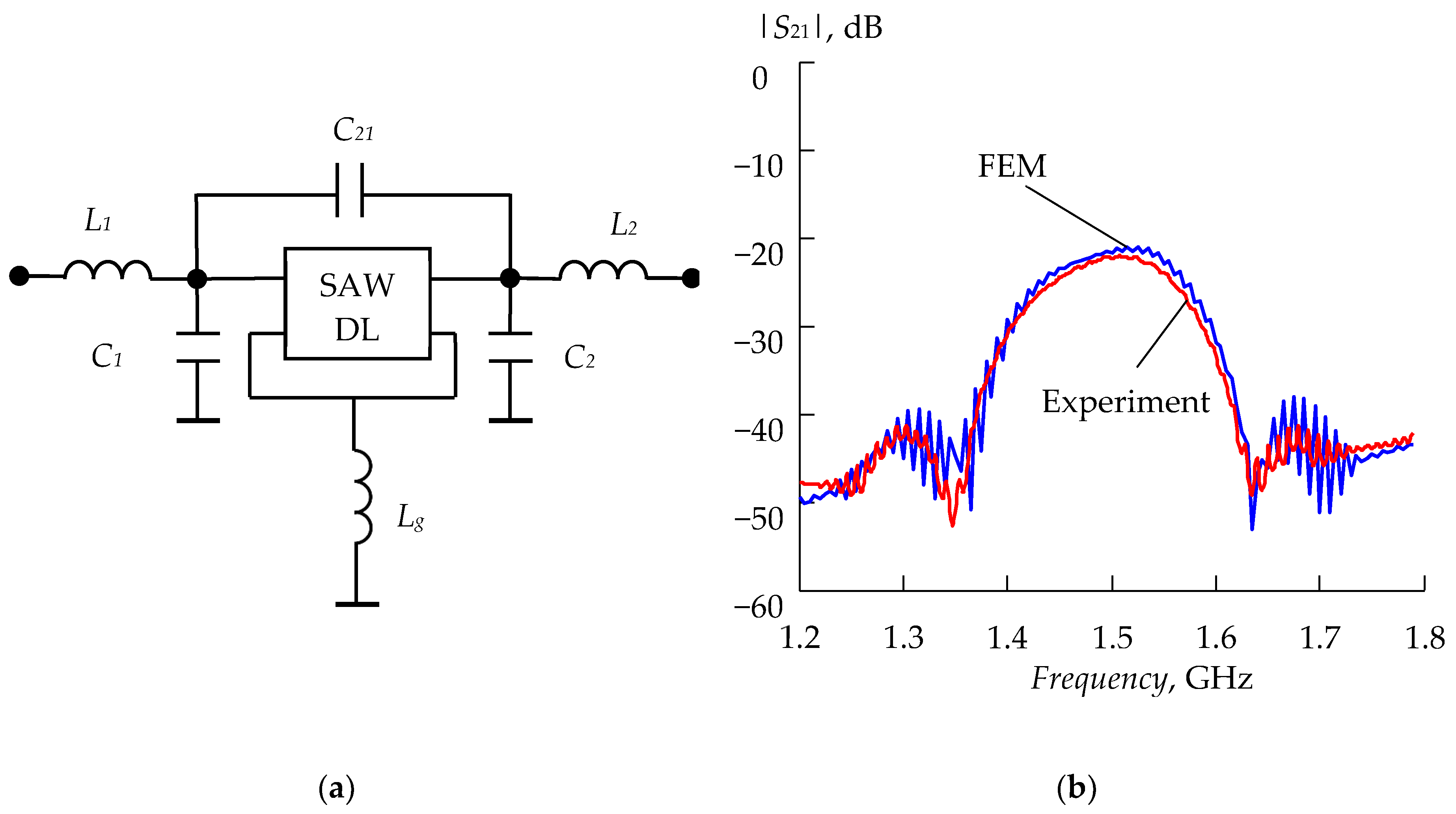
3.2. Delay Line
4. Discussion
5. Conclusions
Funding
Data Availability Statement
Acknowledgments
Conflicts of Interest
References
- Warder, P.; Link, A. Golden Age for Filter Design: Innovative and Proven Approaches for Acoustic Filter, Duplexer, and Multiplexer Design. IEEE Microw. Mag. 2015, 16, 60–72. [Google Scholar] [CrossRef]
- Bauer, T.; Eggs, C.; Wagner, K.; Hagn, P. A Bright Outlook for Acoustic Filtering: A New Generation of Very Low-Profile SAW, TC SAW, and BAW Devices for Module Integration. IEEE Microw. Mag. 2015, 16, 73–81. [Google Scholar] [CrossRef]
- Hashimoto, K.-Y.; Omori, T.; Yamaguchi, M. Design considerations on wideband longitudinally-coupled double-mode SAW filters. In Proceedings of the 2002 IEEE Ultrasonics Symposium, Munich, Germany, 8–11 October 2002; pp. 153–157. [Google Scholar] [CrossRef]
- Loseu, A.S. Novel LSAW DMS filter structure for narrow duplex gap SE->Bal RX filter application. In Proceedings of the 2016 IEEE International Ultrasonics Symposium (IUS), San Diego, CA, USA, 11–14 October 2010; pp. 1258–1262. [Google Scholar] [CrossRef]
- Malocha, S.; Gamble, K.J.; Dong, H.; Dharmalingam, A. Automated COM parameter extraction for SiO2/LiNbO3 and SiO2/LiTaO3 substrates. In Proceedings of the 2016 IEEE International Ultrasonics Symposium (IUS), Tours, France, 18–21 September 2016; pp. 1–4. [Google Scholar] [CrossRef]
- Plessky, V.; Koskela, J.; Willemsen, B.A.; Turner, P.J.; Iliev, F.; Hammond, R.B.; Fenzi, N.O. FEM modeling of an entire 5-IDT CRF/DMS filter. In Proceedings of the 2017 IEEE International Ultrasonics Symposium (IUS), Washington, DC, USA, 6–9 September 2017; pp. 1–5. [Google Scholar] [CrossRef]
- Iyama, A.; Li, X.; Bao, J.; Matsuoka, N.; Omori, T.; Hashimoto, K.-Y. Full 3D FEM Analysis of Scattering at a Border Between IDT and Reflector in SAW Resonators. In Proceedings of the 2019 IEEE International Ultrasonics Symposium (IUS), Glasgow, UK, 6–9 October 2019; pp. 1235–1238. [Google Scholar] [CrossRef]
- Zhang, Y.-M.; Jin, J.; Li, H.-L.; Hu, H.-P. A Novel Method to Extract COM Parameters for SAW Based on FEM. In Proceedings of the 2019 13th Symposium on Piezoelectrcity, Acoustic Waves and Device Applications (SPAWDA), Harbin, China, 11–14 January 2019; pp. 1–5. [Google Scholar] [CrossRef]
- Plessky, V.; Koskela, J. COUPLING-OF-MODES ANALYSIS OF SAW DEVICES. Int. J. High Speed Electron. Syst. 2000, 10, 867–947. [Google Scholar] [CrossRef]
- Dmitriev, V.F. Modified equations of coupled surface acoustic waves. Journal of Communications Technology and Electronics 2009, 54, 1134–1143. [Google Scholar] [CrossRef]
- Orlov, V.S. Wideband Two-Mode Leaky Surface Acoustic Wave Filter with Non-Equdistant Elecrodes of Transducers and Reflecting Gratings. T-Comm. 2019, 13, 36–45. [Google Scholar]
- Sveshnikov, B. Discrete analysis of regular systems. In Proceedings of the IEEE International Ultrasonics Symposium, San Diego, CA, USA, 11–14 October 2010; pp. 1890–1893. [Google Scholar] [CrossRef]
- Rukhlenko, A.S. Nodal analysis of multitransducer SAW devices. In Proceedings of the 1995 IEEE Ultrasonics Symposium, Seattle, WA, USA, 7–10 November 2002; pp. 297–300. [Google Scholar] [CrossRef]
- Shimko, A.; Plessky, V. Fast SAW Device Simulation in COMSOL Using the Hierarchical Cascading Method. In Proceedings of the 2018 IEEE International Ultrasonics Symposium, Kobe, Japan, 22–25 October 2018; pp. 1–3. [Google Scholar] [CrossRef]
- Koigerov, A.S.; Korlyakov, A.V. Finite Element Modeling of Surface Acoustic Wave Devices Using COMSOL. Russ. Microelectron. 2022, 51, 226–235. [Google Scholar] [CrossRef]
- Zhgoon, S.; Shvetsov, A.; Patel, M.; Bhattacharjee, K. In-situ monitored deposition of SiO2 on longitudinal wave based resonator. In Proceedings of the 2009 IEEE International Ultrasonics Symposium, Roma, Italy, 21 September 2009; pp. 2647–2650. [Google Scholar] [CrossRef]
- Tang, G.; Goto, R.; Nakamura, H. Modeling and Suppression Method for Guided Mode in TC-SAW Devices. In Proceedings of the 2019 IEEE International Ultrasonics Symposium (IUS), Glasgow, UK, 6–9 October 2019; pp. 2087–2090. [Google Scholar] [CrossRef]
- Zhang, Q.; Chen, Z.; Chen, Y.; Dong, J.; Tang, P.; Fu, S.; Wu, H.; Ma, J.; Zhao, X. Periodic Analysis of Surface Acoustic Wave Resonator with Dimensionally Reduced PDE Model Using COMSOL Code. Micromachines 2021, 12, 141. [Google Scholar] [CrossRef] [PubMed]
- Hao, W.C.; Wei LU, O.; Zhao, G.H.; Jiao, H.L.; Yin, Y.G. FEM analysis of response mechanism for temperature sensors based on surface acoustic wave resonators. In Proceedings of the 2019 13th Symposium on Piezoelectricity, Acoustic Waves and Device Applications (SPAWDA), Harbin, China, 11–14 January 2019; pp. 1–5. [Google Scholar] [CrossRef]
- Shen, J.; Fu, S.; Su, R.; Xu, H.; Zeng, F.; Song, C.; Pan, F. Systematical Study of the Basic Properties of Surface Acoustic Wave Devices Based on ZnO and GaN Multilayers. Electronics 2020, 10, 23. [Google Scholar] [CrossRef]
- Jean Claude, A.O.; Eloi Jean Jacques, B.; Gaston, N.M.; Adoum, T.N.; Elysée, O.N.; Omar, E. Modeling and Electrical Char-acterization of a Bilayer Pt/AlN/Sapphire One Port Resonator for Sensor Applications. Electronics 2021, 10, 370. [Google Scholar] [CrossRef]
- Ma, R.; Liu, W.; Sun, X.; Zhou, S.; Lin, D. FEM Simulation of a High-Performance 128 Y–XLiNbO3/SiO2/Si Functional Sub-strate for Surface Acoustic Wave Gyroscopes. Micromachines 2022, 13, 202. [Google Scholar] [CrossRef] [PubMed]
- Shevchenko, S.Y.; Mikhailenko, D.A. Topological Optimization of Circular SAW Resonators: Overcoming the Discreteness Effects. Sensors 2022, 22, 1172. [Google Scholar] [CrossRef] [PubMed]
- Koigerov, A.S.; Balysheva, O.L. Numerical Analysis of Parameters of Pseudosurface Acoustic Waves in Lithium Niobate and Tantalate Crystals. J. Commun. Technol. Electron. 2021, 66, 1388–1395. [Google Scholar] [CrossRef]
- Dvoesherstov, M.Y.; Cherednik, V.I.; Bosov, S.I.; Orlov, I.Y.; Rudenko, O.V. Numerical and experimental analysis of the parameters of an electroacoustic thin-film microwave resonator. Acoust. Phys. 2013, 59, 513–520. [Google Scholar] [CrossRef]
- Sun, X.; Ma, R.; Zhou, S.; Shao, X.; Cheng, J.; Lin, D.; Wang, W.; Liu, W. Fast, Accurate and Full Extraction of Coupling-of-Modes Parameters by Finite Element Method. Crystals 2022, 12, 706. [Google Scholar] [CrossRef]
- Dmitriev, V.F.; Koigerov, A.S. Study of Surface Acoustic Wave ID Tags with Specified Correlation Propertieces. J. Commun. Technol. Electron. 2011, 56, 1256–1265. [Google Scholar] [CrossRef]
- Sveshnikov, B.V.; Bagdasaryan, A.S. The Main Principles of Formation of the Transverse Modes in the Multilayered Wave-guides of Surface Acoustic Waves. Radiophys Quantum 2016, 59, 97–110. [Google Scholar] [CrossRef]
- Morita, T.; Watanabe, Y.; Tanaka, M.; Nakazawa, Y. Wideband low loss double mode SAW filters. In Proceedings of the IEEE 1992 Ultrasonics Symposium, Tucson, AZ, USA, 20–23 October 1992; Volume 1, pp. 95–104. [Google Scholar] [CrossRef]
- Campbell, C. Obtaining the fundamental and harmonic radiation conductances of a reflective SAW interdigital transducer. In Proceedings of the IEEE Ultrasonics Symposium, Sendai, Japan, 05–08 October 1998; Volume 1, pp. 169–173. [Google Scholar] [CrossRef]
- Koigerov, A.S.; Balysheva, O.L. Finite element simulation of SAW delay line operating with the use of third harmonic frequency. Comput. Telecommun. Control. 2022, 15, 40–50. [Google Scholar] [CrossRef]
- Available online: https://www.ndk.com/catalog/AN-SD_GG_e.pdf (accessed on 13 November 2022).


| Parameter | FEM | COM |
|---|---|---|
| Mesh discretization, wavelengths | 1/12 | - |
| Number of elements (mesh statistics) | 157,738 | - |
| Required RAM, GB | 29.23 | - |
| Number of degrees of freedom (DOF) | 3,105,240 | - |
| Number of frequency points | 201 | 201 |
| Computation time | ~16 h 30 min | 2 s |
| Bandpass at level of –1 dB, MHz | 24.4 | 24.6 |
| Insertion loss, dB | –0.29 | –0.32 |
| Passband ripple, dB | 0.6 | 0.45 |
| Central frequency, MHz | 540.25 | 540.45 |
Publisher’s Note: MDPI stays neutral with regard to jurisdictional claims in published maps and institutional affiliations. |
© 2022 by the author. Licensee MDPI, Basel, Switzerland. This article is an open access article distributed under the terms and conditions of the Creative Commons Attribution (CC BY) license (https://creativecommons.org/licenses/by/4.0/).
Share and Cite
Koigerov, A.S. Modern Physical-Mathematical Models and Methods for Design Surface Acoustic Wave Devices: COM Based P-Matrices and FEM in COMSOL. Mathematics 2022, 10, 4353. https://doi.org/10.3390/math10224353
Koigerov AS. Modern Physical-Mathematical Models and Methods for Design Surface Acoustic Wave Devices: COM Based P-Matrices and FEM in COMSOL. Mathematics. 2022; 10(22):4353. https://doi.org/10.3390/math10224353
Chicago/Turabian StyleKoigerov, Aleksey S. 2022. "Modern Physical-Mathematical Models and Methods for Design Surface Acoustic Wave Devices: COM Based P-Matrices and FEM in COMSOL" Mathematics 10, no. 22: 4353. https://doi.org/10.3390/math10224353