
Dual-Band Rectifier Circuit Design for IoT Communication in 5G Systems

 ,
,  ,
,  ,
,  and
and 
Abstract
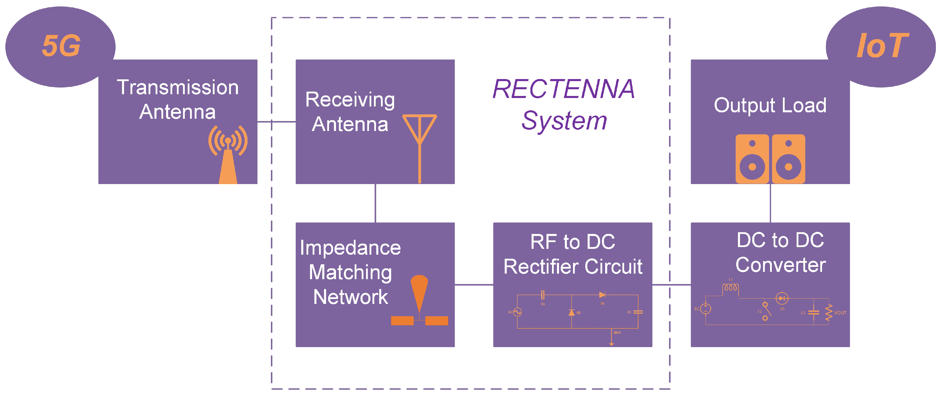
:1. Introduction
- We present a novel dual-band rectifier circuit for the 5G FR1 zone.
- We discuss and provide a complete design framework for a low-cost RF-to-DC rectifier.
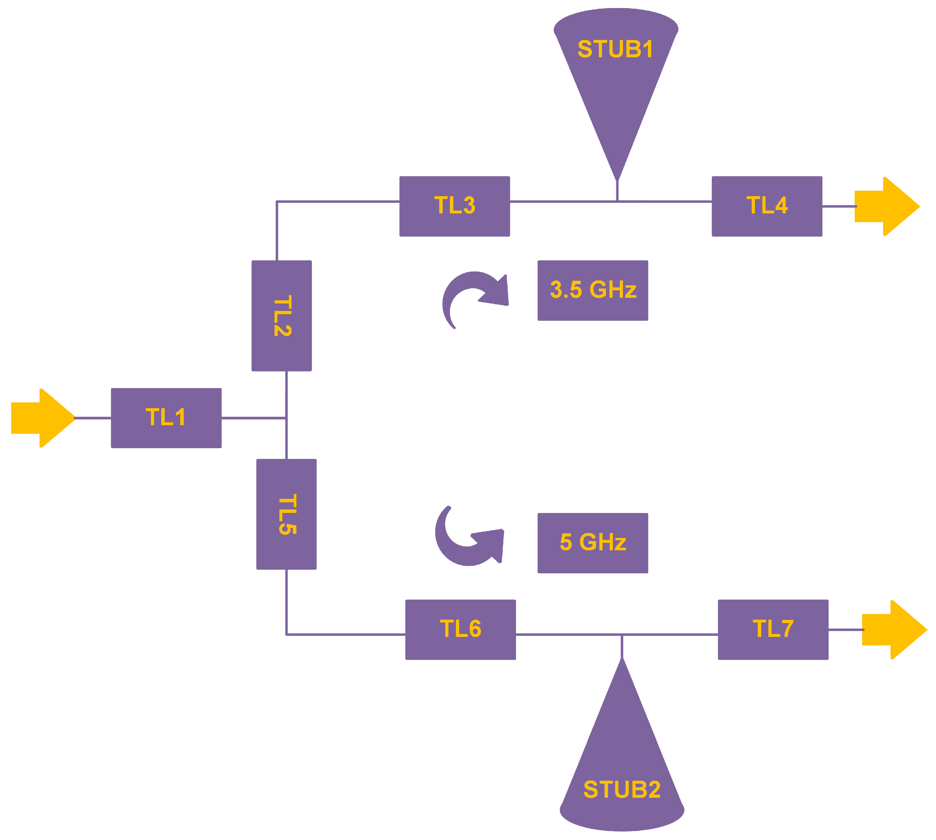
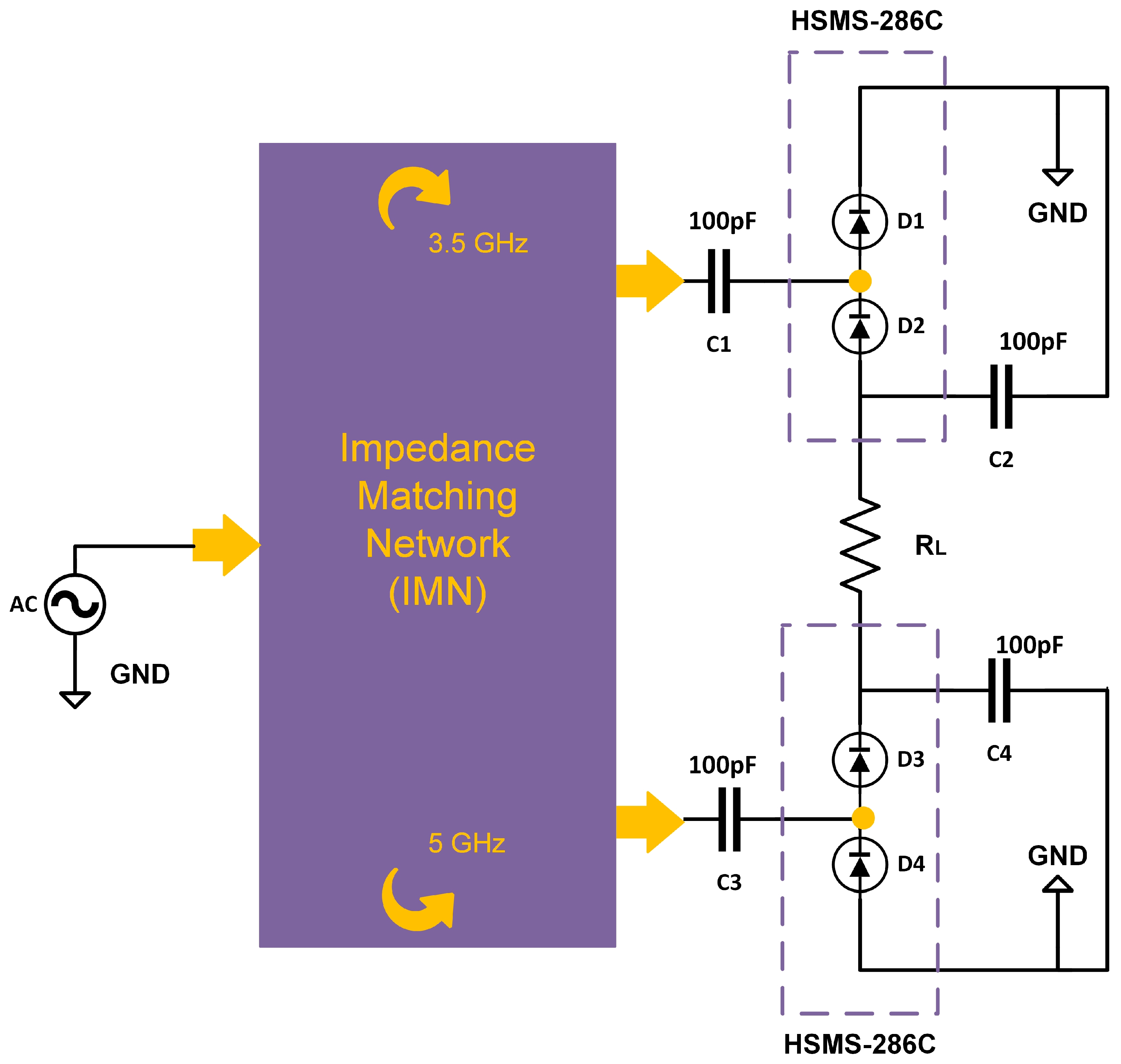
- We propose a novel impedance-matching network that consists of two distinct branches, one for 3.5 GHz and the other for 5 GHz. Each branch consists of a T-shaped network with rectangular and radial stubs.
- We design a circuit design that works at 2 sub-6 GHz 5G bands, ( and 5 GHz) simultaneously.
2. Materials and Methods
2.1. Related Work
2.2. Design Methodology
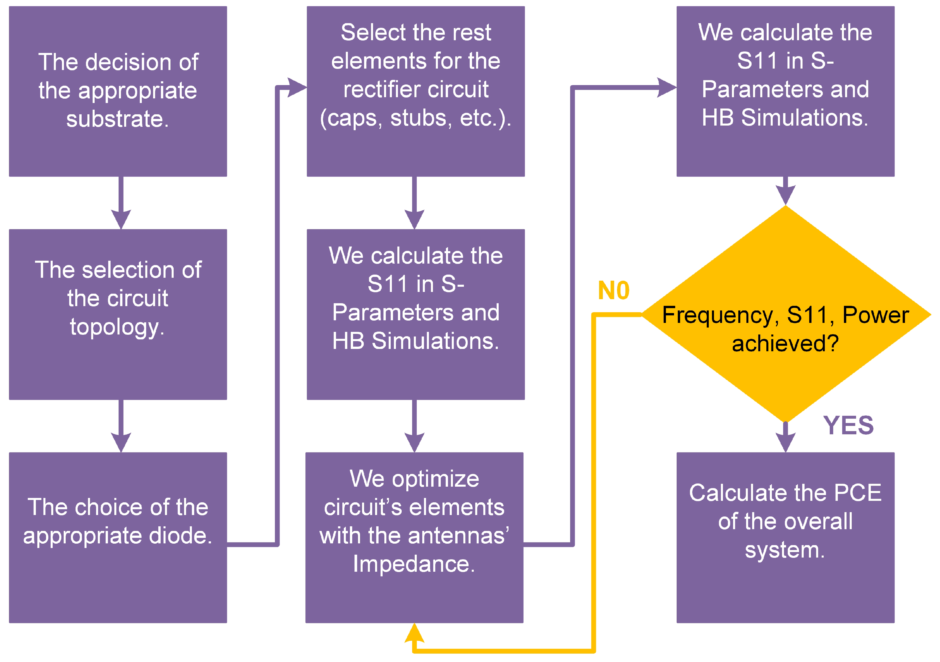
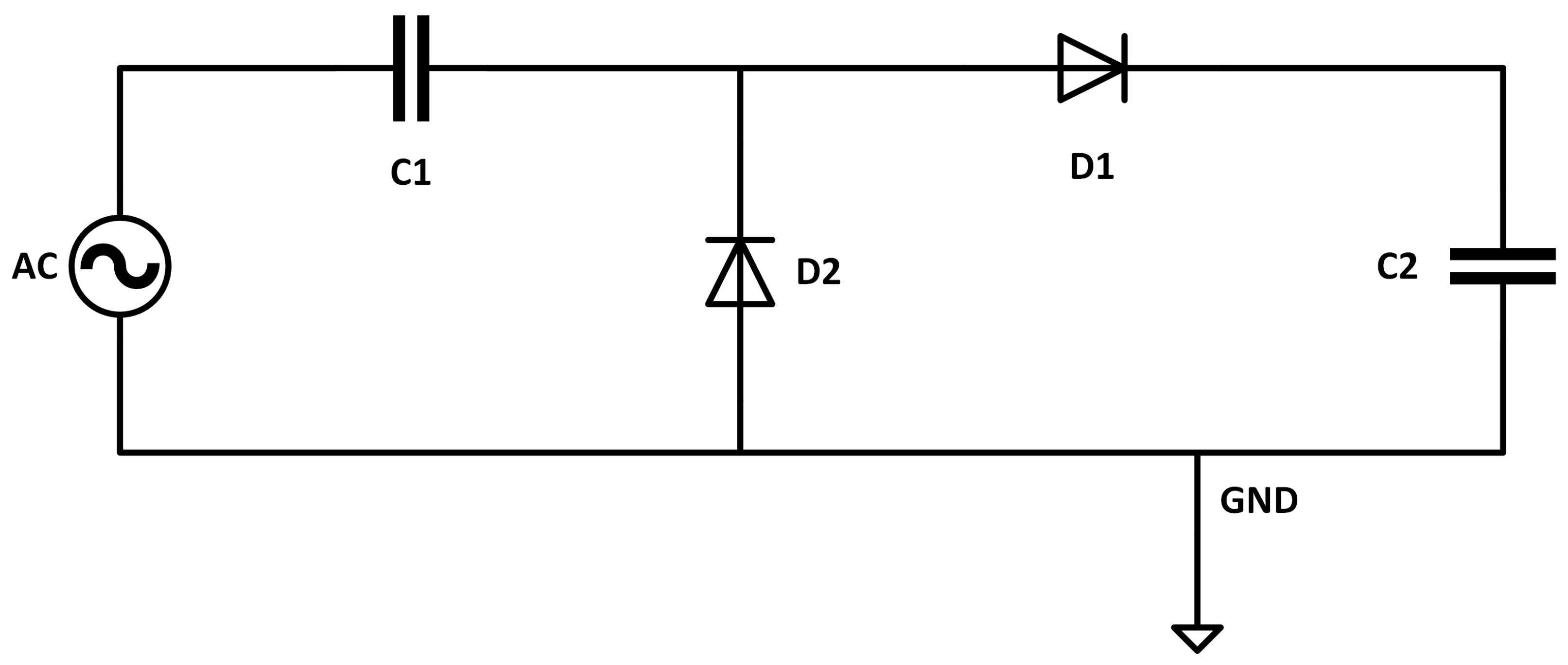
3. Design Framework
3.1. Substrate Selection
3.2. Topology Selection
3.3. Diode Selection
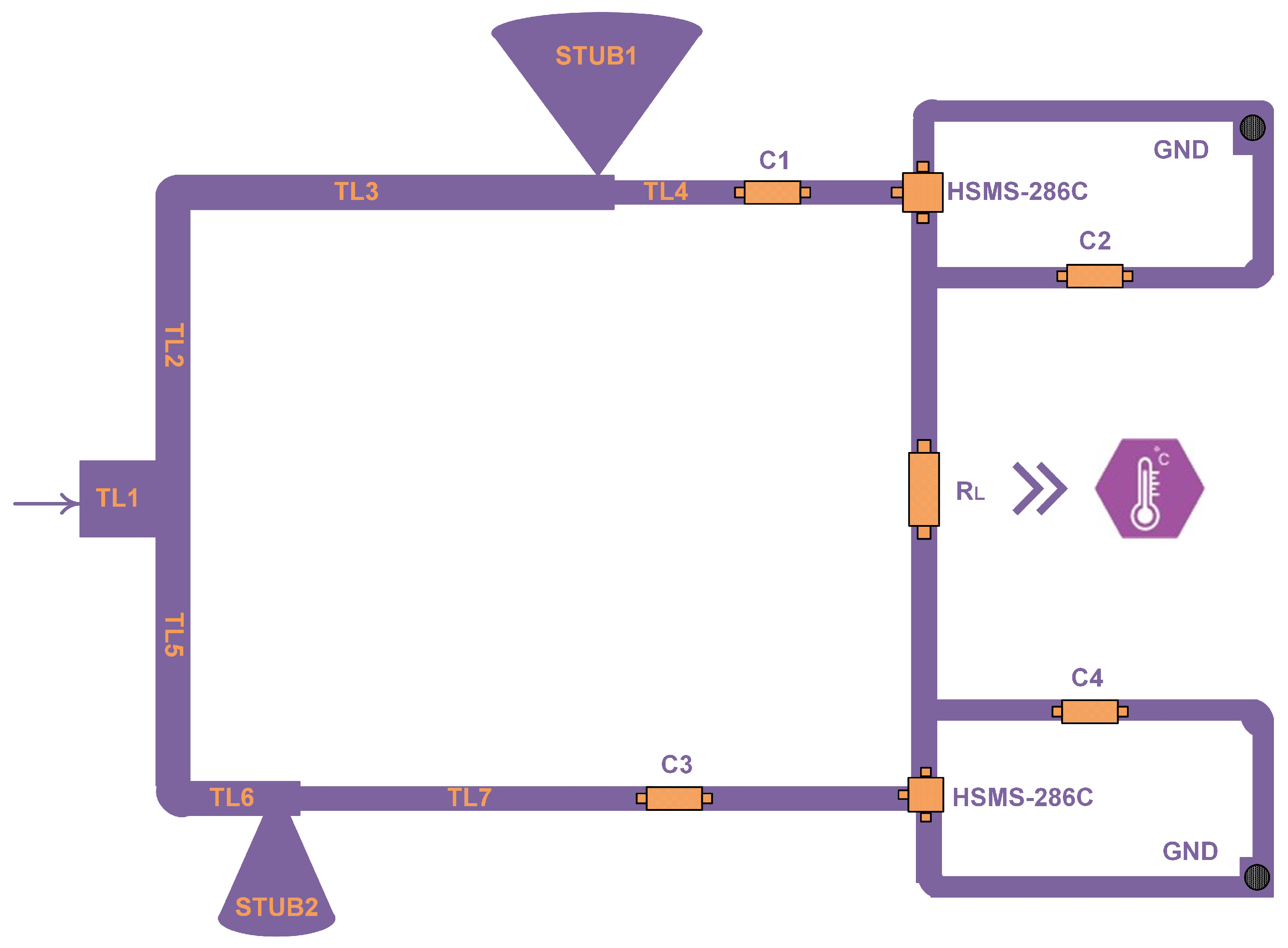
3.4. Impedance-Matching Network Design
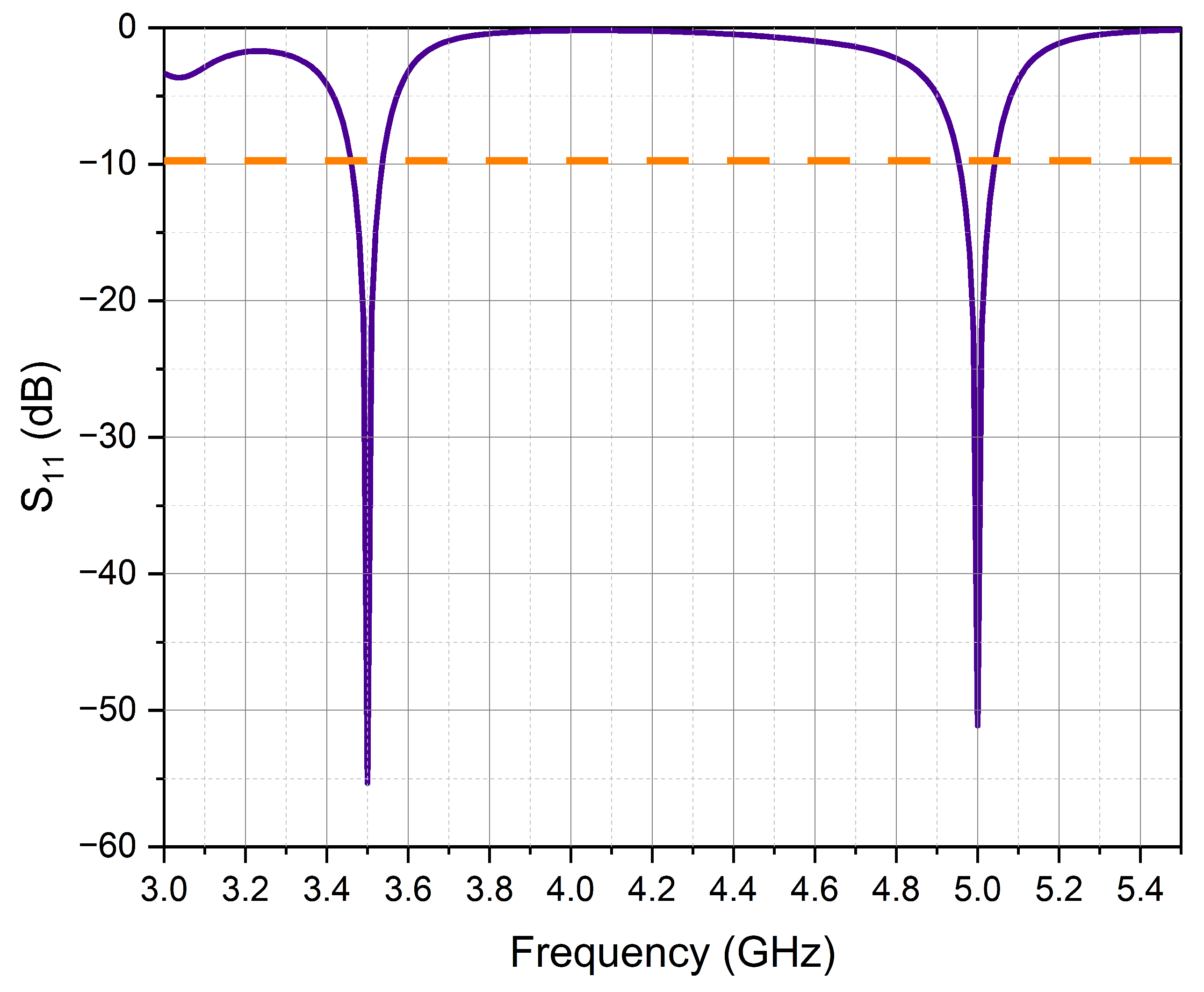
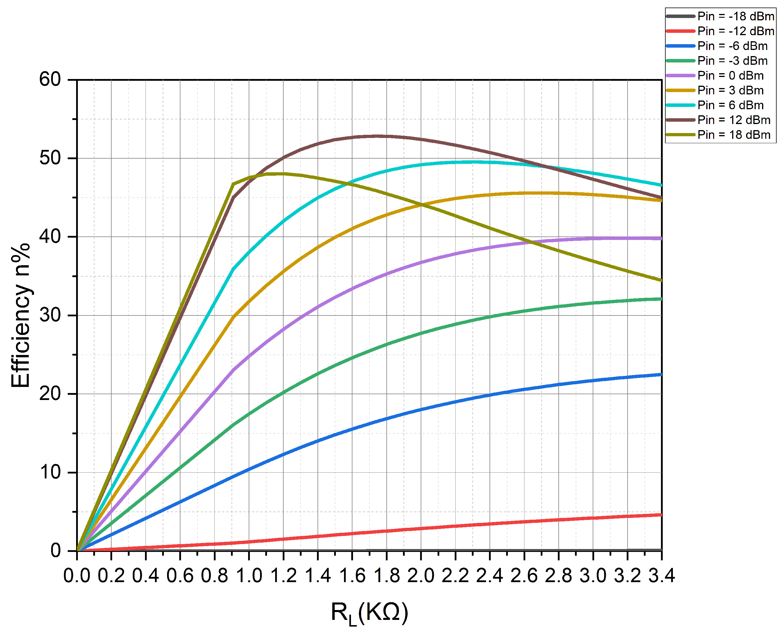
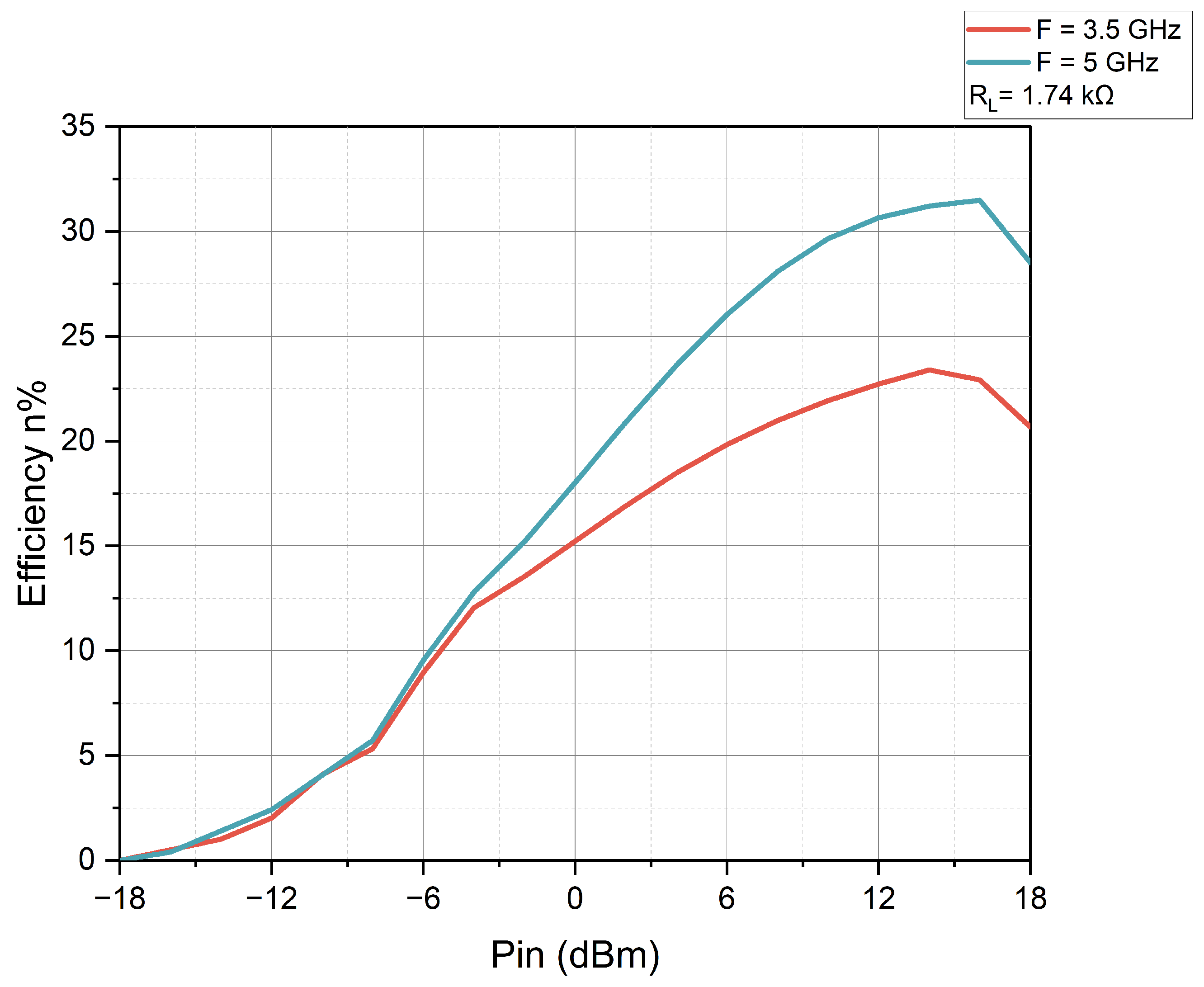
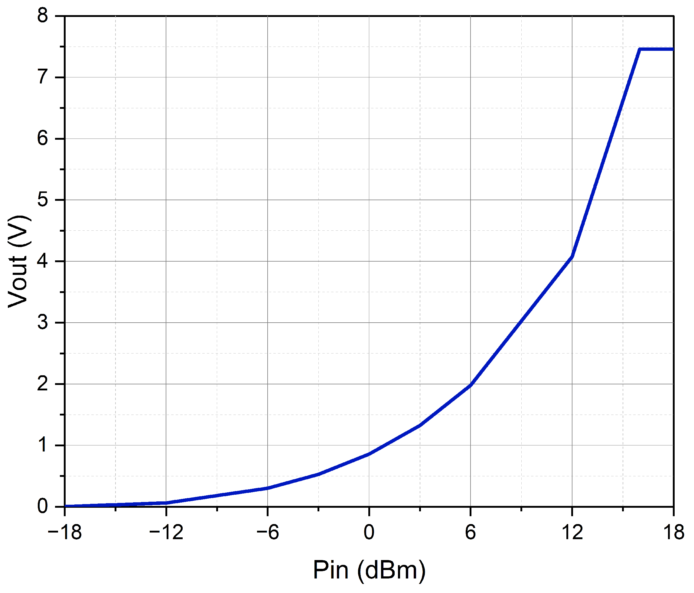
4. Numerical Results
5. Discussion
6. Conclusions
Author Contributions
Funding
Data Availability Statement
Conflicts of Interest
References
- Roda-Sanchez, L.; Garrido-Hidalgo, C.; Hortelano, D.; Olivares, T.; Ruiz, M.C. OperaBLE: An IoT-based wearable to improve efficiency and smart worker care services in Industry 4.0. J. Sens. 2018, 2018, 6272793. [Google Scholar] [CrossRef]
- Boursianis, A.D.; Papadopoulou, M.S.; Damantoulakis, P.; Karampatea, A.; Doanis, P.; Geourgoulas, D.; Skoufa, A.; Valavanis, D.; Apostolidis, C.; Babas, D.G.; et al. Advancing Rational Exploitation of Water Irrigation Using 5G-IoT Capabilities: The AREThOU5A Project. In Proceedings of the 2019 29th International Symposium on Power and Timing Modeling, Optimization and Simulation (PATMOS), Rhodes, Greece, 1–3 July 2019; pp. 127–132. [Google Scholar] [CrossRef]
- What is the Internet of Things (IoT)? 2022. Available online: https://www.techtarget.com/iotagenda/definition/Internet-of-Things-IoT (accessed on 14 September 2022).
- Rappaport, T.S.; Xing, Y.; MacCartney, G.R.; Molisch, A.F.; Mellios, E.; Zhang, J. Overview of Millimeter Wave Communications for Fifth-Generation (5G) Wireless Networks—With a Focus on Propagation Models. IEEE Trans. Antennas Propag. 2017, 65, 6213–6230. [Google Scholar] [CrossRef]
- Tseliou, G.; Adelantado, F.; Verikoukis, C. A Base Station Agnostic Network Slicing Framework for 5G. IEEE Netw. 2019, 33, 82–88. [Google Scholar] [CrossRef]
- What Is 5G? Available online: https://www.cisco.com/c/en/us/solutions/what-is-5g.html (accessed on 31 January 2023).
- Song, C.; Ding, Y.; Eid, A.; Hester, J.G.D.; He, X.; Bahr, R.; Georgiadis, A.; Goussetis, G.; Tentzeris, M.M. Advances in Wirelessly Powered Backscatter Communications: From Antenna/RF Circuitry Design to Printed Flexible Electronics. Proc. IEEE 2022, 110, 171–192. [Google Scholar] [CrossRef]
- Daskalakis, S.N.; Georgiadis, A.; Tentzeris, M.M.; Goussetis, G.; Deligeorgis, G. The New Era of Long-Range “Zero-Interception” Ambient Backscattering Systems: 130 m with 130 nA Front-End Consumption. Sensors 2022, 22, 4151. [Google Scholar] [CrossRef]
- Costa, C.M.d.; Baltus, P. Design Methodology for Industrial Internet-of-Things Wireless Systems. IEEE Sens. J. 2021, 21, 5529–5542. [Google Scholar] [CrossRef]
- Pliatsios, D.; Sarigiannidis, P.; Goudos, S.; Karagiannidis, G.K. Realizing 5G vision through Cloud RAN: Technologies, challenges, and trends. EURASIP J. Wirel. Commun. Netw. 2018, 2018, 1–15. [Google Scholar] [CrossRef] [Green Version]
- Rappaport, T.S.; Sun, S.; Mayzus, R.; Zhao, H.; Azar, Y.; Wang, K.; Wong, G.N.; Schulz, J.K.; Samimi, M.; Gutierrez, F. Millimeter Wave Mobile Communications for 5G Cellular: It Will Work! IEEE Access 2013, 1, 335–349. [Google Scholar] [CrossRef]
- Esteves, V.; Antonopoulos, A.; Kartsakli, E.; Puig-Vidal, M.; Miribel-Català, P.; Verikoukis, C. Cooperative Energy Harvesting-Adaptive MAC Protocol for WBANs. Sensors 2015, 15, 12635–12650. [Google Scholar] [CrossRef] [Green Version]
- Rangan, S.; Rappaport, T.S.; Erkip, E. Millimeter-Wave Cellular Wireless Networks: Potentials and Challenges. Proc. IEEE 2014, 102, 366–385. [Google Scholar] [CrossRef] [Green Version]
- Mekikis, P.V.; Lalos, A.S.; Antonopoulos, A.; Alonso, L.; Verikoukis, C. Wireless Energy Harvesting in Two-Way Network Coded Cooperative Communications: A Stochastic Approach for Large Scale Networks. IEEE Commun. Lett. 2014, 18, 1011–1014. [Google Scholar] [CrossRef]
- Palazzi, V.; Correia, R.; Gu, X.; Hemour, S.; Wu, K.; Costanzo, A.; Masotti, D.; Fazzini, E.; Georgiadis, A.; Kazemi, H.; et al. Radiative Wireless Power Transfer: Where We Are and Where We Want to Go. IEEE Microw. Mag. 2023, 24, 57–79. [Google Scholar] [CrossRef]
- Bi, S.; Ho, C.K.; Zhang, R. Wireless powered communication: Opportunities and challenges. IEEE Commun. Mag. 2015, 53, 117–125. [Google Scholar] [CrossRef] [Green Version]
- Parzysz, F.; Ntontin, K.; Kalaboukas, K.; Verikoukis, C. Dedicated RF Power Transfer for Wirelessly-Powered Wearable Medical Sensors. In Proceedings of the 2016 IEEE Global Communications Conference (GLOBECOM), Washington, DC, USA, 4–8 December 2016; pp. 1–6. [Google Scholar] [CrossRef]
- Otal, B.; Alonso, L.; Verikoukis, C. Energy-efficiency analysis of a distributed queuing medium access control protocol for biomedical wireless sensor networks in saturation conditions. Sensors 2011, 11, 1277–1296. [Google Scholar] [CrossRef] [Green Version]
- Mirzababaee, N.; Geran, F.; Mohanna, S. A radio frequency energy harvesting rectenna for GSM, LTE, WLAN, and WiMAX. Int. J. RF Microw. Comput.-Aided Eng. 2021, 31, e22630. [Google Scholar] [CrossRef]
- Brown, W.C. The history of power transmission by radio waves. IEEE Trans. Microw. Theory Tech. 1984, 32, 1230–1242. [Google Scholar] [CrossRef] [Green Version]
- Mishra, D.; De, S.; Jana, S.; Basagni, S.; Chowdhury, K.; Heinzelman, W. Smart RF energy harvesting communications: Challenges and opportunities. IEEE Commun. Mag. 2015, 53, 70–78. [Google Scholar] [CrossRef] [Green Version]
- Forouzesh, M.; Siwakoti, Y.P.; Gorji, S.A.; Blaabjerg, F.; Lehman, B. Step-Up DC–DC Converters: A Comprehensive Review of Voltage-Boosting Techniques, Topologies, and Applications. IEEE Trans. Power Electron. 2017, 32, 9143–9178. [Google Scholar] [CrossRef]
- Ibrahim, H.H.; Singh, M.J.; Al-Bawri, S.S.; Ibrahim, S.K.; Islam, M.T.; Alzamil, A.; Islam, M.S. Radio frequency energy harvesting technologies: A comprehensive review on designing, methodologies, and potential applications. Sensors 2022, 22, 4144. [Google Scholar] [CrossRef]
- Belleville, M.; Cantatore, E.; Fanet, H.; Fiorini, P.; Nicole, P.; Pelgrom, M.; Piguet, C.; Hahn, R.; Van Hoof, C.; Vullers, R.; et al. Energy Autonomous Systems: Future Trends in Devices, Technology, and Systems; CATRENE: Paris, France, 2009. [Google Scholar]
- De Vito, L.; Cocca, V.; Riccio, M.; Tudosa, I. Wireless Active Guardrail System for environmental measurements. In Proceedings of the 2012 IEEE Workshop on Environmental Energy and Structural Monitoring Systems (EESMS), Perugia, Italy, 28 September 2012; pp. 50–57. [Google Scholar] [CrossRef]
- Chen, C.; Jiang, J.; Zhou, Y.; Lv, N.; Liang, X.; Wan, S. An edge intelligence empowered flooding process prediction using Internet of things in smart city. J. Parallel Distrib. Comput. 2022, 165, 66–78. [Google Scholar] [CrossRef]
- Chen, C.; Li, H.; Li, H.; Fu, R.; Liu, Y.; Wan, S. Efficiency and Fairness Oriented Dynamic Task Offloading in Internet of Vehicles. IEEE Trans. Green Commun. Netw. 2022, 6, 1481–1493. [Google Scholar] [CrossRef]
- Liu, S.; Yu, J.; Deng, X.; Wan, S. FedCPF: An Efficient-Communication Federated Learning Approach for Vehicular Edge Computing in 6G Communication Networks. IEEE Trans. Intell. Transp. Syst. 2022, 23, 1616–1629. [Google Scholar] [CrossRef]
- Lu, J.; Liu, H.; Zhang, Z.; Wang, J.; Goudos, S.; Wan, S. Toward Fairness-Aware Time-Sensitive Asynchronous Federated Learning for Critical Energy Infrastructure. IEEE Trans. Ind. Inform. 2022, 18, 3462–3472. [Google Scholar] [CrossRef]
- Lu, J.; Liu, H.; Jia, R.; Wang, J.; Sun, L.; Wan, S. Towards Personalized Federated Learning Via Group Collaboration in IIoT. IEEE Trans. Ind. Inform. 2022, 1–10. [Google Scholar] [CrossRef]
- 3GPP: 5G-NR Specifications Series. Available online: https://www.3gpp.org/dynareport?code=38-series.htm (accessed on 14 September 2022).
- 5G Frequency Bands & Spectrum Allocations. 2021. Available online: https://www.cablefree.net/wirelesstechnology/4glte/5g-frequency-bands-lte/ (accessed on 14 September 2022).
- 5G FR1 Frequency Bands. 2021. Available online: https://www.everythingrf.com/community/5g-fr1-frequency-bands (accessed on 14 September 2022).
- Dilli, R. Analysis of 5G Wireless Systems in FR1 and FR2 Frequency Bands. In Proceedings of the 2020 2nd International Conference on Innovative Mechanisms for Industry Applications (ICIMIA), Bangalore, India, 5–7 March 2020; pp. 767–772. [Google Scholar] [CrossRef]
- 5G Frequency Bands, Channels for FR1 & FR2. 2021. Available online: https://www.electronics-notes.com/articles/connectivity/5g-mobile-wireless-cellular/frequency-bands-channels-fr1-fr2.php (accessed on 14 September 2022).
- Dehghani, S.; Johnson, T. A 2.4-GHz CMOS Class-E Synchronous Rectifier. IEEE Trans. Microw. Theory Tech. 2016, 64, 1655–1666. [Google Scholar] [CrossRef]
- Chatterjee, S.; Tarique, M. A 100-nW Sensitive RF-to-DC CMOS Rectifier for Energy Harvesting Applications. In Proceedings of the 2016 29th International Conference on VLSI Design and 2016 15th International Conference on Embedded Systems (VLSID), Kolkata, India, 4–8 January 2016; pp. 557–558. [Google Scholar] [CrossRef]
- Jantarachote, V.; Tontisirin, S.; Akkaraekthalin, P.; Negra, R.; Chalermwisutkul, S. CMOS rectifier design for RFID chip with high sensitivity at low input power to be combined with an ultrasmall antenna. Int. J. Numer. Model. Electron. Netw. Devices Fields 2019, 32, e2607. [Google Scholar] [CrossRef]
- Rosli, M.; Murad, S.; Norizan, M.; Ramli, M. Design of RF to DC conversion circuit for energy harvesting in CMOS 0.13-μm technology. AIP Conf. Proc. 2018, 2045, 0200892018. [Google Scholar] [CrossRef]
- Lo, Y.L.; Chuang, Y.H. A High-Efficiency CMOS Rectifier with Wide Harvesting Range and Wide Band Based on MPPT Technique for Low-Power IoT System Applications. Circuits Syst. Signal Process. 2017, 36, 5019–5040. [Google Scholar] [CrossRef]
- Basim, M.; Khan, D.; Ain, Q.U.; Shehzad, K.; Shah, S.A.A.; Jang, B.G.; Pu, Y.G.; Yoo, J.M.; Kim, J.T.; Lee, K.Y. A Highly Efficient RF-DC Converter for Energy Harvesting Applications Using a Threshold Voltage Cancellation Scheme. Sensors 2022, 22, 2659. [Google Scholar] [CrossRef]
- Derbal, M.C.; Nedil, M. A high gain dual band rectenna for RF energy harvesting applications. Prog. Electromagn. Res. Lett. 2020, 90, 29–36. [Google Scholar] [CrossRef]
- Eltresy, N.; Eisheakh, D.; Abdallah, E.; Elhenawy, H. RF Energy Harvesting Using Efficiency Dual Band Rectifier. In Proceedings of the 2018 Asia-Pacific Microwave Conference (APMC), Kyoto, Japan, 6–9 November 2018; pp. 1453–1455. [Google Scholar] [CrossRef]
- Zied, C.M.; Rashid, E.R.; Hareb, A. Harvesting microwave energy from WiMax bands based on a Dual-Band Antenna. IOP Conf. Ser. Earth Environ. Sci. 2019, 227, 042044. [Google Scholar] [CrossRef]
- Dardeer, O.M.A.; Elsadek, H.A.; Abdallah, E.A. Compact Broadband Rectenna for Harvesting RF Energy in WLAN and WiMAX Applications. In Proceedings of the 2019 International Conference on Innovative Trends in Computer Engineering (ITCE), Aswan, Egypt, 2–4 February 2019; pp. 292–296. [Google Scholar] [CrossRef]
- Sarma, S.S.; Chandravanshi, S.; Akhtar, M.J. Triple band differential rectifier for RF energy harvesting applications. In Proceedings of the 2016 Asia-Pacific Microwave Conference (APMC), New Delhi, India, 5–9 December 2016; pp. 1–4. [Google Scholar] [CrossRef]
- Azam, S.K.; Islam, M.S.; Hossain, A.Z.; Othman, M. Monopole antenna on transparent substrate and rectifier for energy harvesting applications in 5G. Int. J. Adv. Comput. Sci. Appl. 2020, 11, 84–89. [Google Scholar] [CrossRef]
- Bougas, I.D.; Papadopoulou, M.S.; Boursianis, A.D.; Sarigiannidis, P.; Nikolaidis, S.; Goudos, S.K. Rectifier circuit design for 5G energy harvesting applications. In Proceedings of the 2022 11th International Conference on Modern Circuits and Systems Technologies (MOCAST), Samos, Greece, 3–7 July 2022; pp. 1–4. [Google Scholar] [CrossRef]
- Usman, M.; Khan, W.T. Six Band RF Energy Harvesting From Ambient Signals. 2019. Available online: https://www.mtt.org/app/uploads/2019/01/10-Final-Report_Usman.pdf (accessed on 14 September 2022).
- Jung, Y.H.; Zhang, H.; Lee, I.K.; Shin, J.H.; Kim, T.i.; Ma, Z. Releasable high-performance GaAs Schottky diodes for gigahertz operation of flexible bridge rectifier. Adv. Electron. Mater. 2019, 5, 1800772. [Google Scholar] [CrossRef]
- Mohd Noor, F.S.; Zakaria, Z.; Lago, H.; Meor Said, M.A. Dual-band aperture-coupled rectenna for radio frequency energy harvesting. Int. J. RF Microw. Comput.-Aided Eng. 2019, 29, e21651. [Google Scholar] [CrossRef] [Green Version]
- Yoshida, S.; Fukuda, G.; Kobayashi, Y.; Tashiro, S.; Noji, T.; Nishikawa, K.; Kawasaki, S. The C-band MPT rectifierusing a HEMT without bonding-wire connection for a space health monitoring system. In Proceedings of the 2013 IEEE Wireless Power Transfer (WPT), Perugia, Italy, 15–16 May 2013; pp. 163–166. [Google Scholar]
- Bougas, I.D.; Papadopoulou, M.S.; Boursianis, A.D.; Kokkinidis, K.; Goudos, S.K. State-of-the-Art Techniques in RF Energy Harvesting Circuits. Telecom 2021, 2, 369–389. [Google Scholar] [CrossRef]
- Papadopoulou, M.S.; Boursianis, A.D.; Skoufa, A.; Volos, C.K.; Stouboulos, I.N.; Nikolaidis, S.; Goudos, S.K. Dual-Band RF-to-DC Rectifier with High Efficiency for RF Energy Harvesting Applications. In Proceedings of the 2020 9th International Conference on Modern Circuits and Systems Technologies (MOCAST), Bremen, Germany, 7–9 September 2020; pp. 1–4. [Google Scholar] [CrossRef]
- RT/duroid ®5870/5880: High Frequency Laminates. Available online: https://rogerscorp.com/-/media/project/rogerscorp/documents/advanced-electronics-solutions/english/data-sheets/rt-duroid-5870---5880-data-sheet.pdf (accessed on 14 September 2022).
- Bougas, I.D.; Papadopoulou, M.S.; Psannis, K.; Sarigiannidis, P.; Goudos, S.K. State-of-the-Art Technologies in RF Energy Harvesting Circuits – A Review. In Proceedings of the 2020 3rd World Symposium on Communication Engineering (WSCE), Thessaloniki, Greece, 9–11 October 2020; pp. 18–22. [Google Scholar] [CrossRef]
- Ohira, T. Power efficiency and optimum load formulas on RF rectifiers featuring flow-angle equations. IEICE Electron. Express 2013, 10, 20130230. [Google Scholar] [CrossRef] [Green Version]
- HSMS-286x Series: Surface Mount Microwave Schottky Detector Diodes. Available online: https://gr.mouser.com/datasheet/2/678/V02_1388EN0-1222339.pdf (accessed on 14 September 2022).
- AN5457: RF Matching Network Design Guide for STM32WL Series. Available online: https://www.st.com/resource/en/application_note/an5457-rf-matching-network-design-guide-for-stm32wl-series-stmicroelectronics.pdf (accessed on 14 September 2022).
- Zeng, M.; Andrenko, A.S.; Liu, X.; Zhu, B.; Li, Z.; Tan, H.Z. Differential topology rectifier design for ambient wireless energy harvesting. In Proceedings of the 2016 IEEE International Conference on RFID Technology and Applications (RFID-TA), Shunde, China, 21–23 September 2016; pp. 97–101. [Google Scholar]


| Parameter | Width/Length | Angle |
|---|---|---|
| TL1 | /3 mm | - |
| TL2 | / mm | - |
| TL3 | / mm | - |
| TL4 | 1/ mm | - |
| TL5 | / mm | - |
| TL6 | /3 mm | - |
| TL7 | 1/ mm | - |
| STUB1 | 700 nm/6.9 mm | 67 degrees |
| STUB2 | / mm | degrees |
| Reference | Type of Circuit | Substrate | Diode | Frequency (GHz) | (dBm) | (kΩ) | PCE (%) @ Desired Frequencies | |
|---|---|---|---|---|---|---|---|---|
| [42] | Half-Wave rectifier | RT/Duroid 5880 | SMS-7630 | , | 0 | 44 | mV | |
| [43] | Half-Wave rectifier | FR-4 | SMS-7630 | , | - | - | ||
| [44] | Full-Wave rectifier | FR-4 | HSMS-2820 | , | 20 | V | ||
| [45] | Full-Wave rectifier | FR-4 | HSMS-2860 | 6 | 1 | V | ||
| [46] | Full-Wave rectifier | FR-4 | HSMS-286C | , , | 14 | 3 | 42 | V |
| [47] | Full-Wave rectifier | Rogers RO3003 | SMS- LF | 0 | 2 | 42 | - | |
| [48] | Full-Wave rectifier | RT/Duroid 5880 | HSMS-286C | 9 | - | |||
| [49] | Full-Wave rectifier | - | SMS-7630 | , , , , 5 | - | (@ GHz) | V | |
| [50] | Full-Wave rectifier | - | Gallium Arsenide printed diodes | 5 | - | - | - | |
| [51] | Full-Wave rectifier | FR-4 | HSMS-286B | , 5 | 0 | V | ||
| [52] | Full-Wave rectifier | - | - | 15 | - | |||
| This Work | Full-Wave rectifier | RT/Duroid 5880 | HSMS-286C | , 5 | 12 | 53 | V |
Disclaimer/Publisher’s Note: The statements, opinions and data contained in all publications are solely those of the individual author(s) and contributor(s) and not of MDPI and/or the editor(s). MDPI and/or the editor(s) disclaim responsibility for any injury to people or property resulting from any ideas, methods, instructions or products referred to in the content. |
© 2023 by the authors. Licensee MDPI, Basel, Switzerland. This article is an open access article distributed under the terms and conditions of the Creative Commons Attribution (CC BY) license (https://creativecommons.org/licenses/by/4.0/).
Share and Cite
Bougas, I.D.; Papadopoulou, M.S.; Boursianis, A.D.; Nikolaidis, S.; Goudos, S.K. Dual-Band Rectifier Circuit Design for IoT Communication in 5G Systems. Technologies 2023, 11, 34. https://doi.org/10.3390/technologies11020034
Bougas ID, Papadopoulou MS, Boursianis AD, Nikolaidis S, Goudos SK. Dual-Band Rectifier Circuit Design for IoT Communication in 5G Systems. Technologies. 2023; 11(2):34. https://doi.org/10.3390/technologies11020034
Chicago/Turabian StyleBougas, Ioannis D., Maria S. Papadopoulou, Achilles D. Boursianis, Spyridon Nikolaidis, and Sotirios K. Goudos. 2023. "Dual-Band Rectifier Circuit Design for IoT Communication in 5G Systems" Technologies 11, no. 2: 34. https://doi.org/10.3390/technologies11020034