Perspective

Methods of Material and Surface Analysis for the Evaluation of Failure Modes for Electrical Connectors

1
Volkswagen AG, 38436 Wolfsburg, Germany
2
Precision Engineering Laboratory, Ostwestfalen-Lippe University of Applied Sciences and Arts, 32657 Lemgo, Germany
*
Author to whom correspondence should be addressed.
Technologies 2022, 10(6), 124; https://doi.org/10.3390/technologies10060124
Submission received: 14 October 2022 / Revised: 25 November 2022 / Accepted: 27 November 2022 / Published: 29 November 2022

Abstract

:
The development of autonomous vehicles and the integration of new information and communication technologies are making the reliability of electrical systems and components in modern vehicles increasingly important. Electrical connectors are a crucial component in an electrical on-board system. They are exposed to a wide variety of influences by the environment and operating conditions. Thus, the degradation of electrical connectors can occur. Material and surface analysis methods are the tools used to analyze the degradation mechanisms in connectors after lifetime tests, as well as in field operations. Within the framework of this study, a wide variety of methods from the analytical scope are presented and discussed. The connector surfaces degraded by different failure mechanisms are analyzed using various material and surface analysis methods. The quality and the nature of the analyses results obtained from various analysis methods are compared. Also, this study deals with the benefits and limitations, as well as the effort and the specific challenges of different material and surface analytical methods for the evaluation of failure mechanisms from the point of view of a material and surface analyst.

1. Introduction

The implementation of electric and hybrid vehicles increases the number of cars with highly complex electronic infrastructures [1]. The increasing degree of integration of new communication and information technologies also reinforces this development [2]. In addition, the development of autonomous driving vehicles also requires especially durable and reliable electrical systems [3,4]. The signal transmission between electrical control units, sensors and other components in the vehicle is ensured by electrical connectors. These connectors have to guarantee safe signal transmission over the lifetime of the vehicle [5]. The described integration of electronics and mechatronics in the vehicle continues to lead to an increase in the number of electrical connectors [6,7]. Electrical connectors in the vehicle are exposed to a wide variety of influences from the environment and operation. These include vibrations and temperature cycles [4,7,8]. Those and other influencing factors can lead to a diversity of damage mechanisms acting on the electrical connectors [3,9]. The different failure modes can influence the reliability and lifetime of a particular electrical contact [2].
In order to prove the reliability and lifetime of electrical connectors, different types of tests are carried out, where they are exposed to external loads and examined after testing using material and surface analytical methods [8,10,11,12]. Likewise, the choice of methods to examine the material and surface properties after the stress test is variegated [2,8,13].
This study deals with different methods of material and surface analysis and their application with regard to electrical connectors. On the basis of exemplary results, the applicability of different analysis methods for a variety of failure mechanisms is shown. Furthermore, the methods are evaluated with regard to the applicability to various degradation mechanisms, the availability as well as the required expertise for the interpretation of the results. Finally, this study deals with recommendations for effective and efficient analyses of electrical connectors.
Analyses of road tested cars makes it possible to determine the main causes of failures occurring in electrical connectors. These include corrosion, oxidation, contamination, diffusion, relaxation and also fretting corrosion [3]. Thus, in the case of electrical connectors, the degradation of the surfaces is carried out by a combination of mechanical, chemical and thermal influencing factors [14]. Therefore, a wide variety of damage mechanisms for electrical connectors are discussed in science [9,15,16]. In the following passage, some of these failures modes are presented.
The mechanism of fretting corrosion is a common cause of failure in electrical connectors and can be described as accelerated aging of a contact due to surface degradation [17] (p. 214), [18]. Vibrations, cyclic loads or temperature changes induce relative movements between the contacted parts, which cause damage to the surface [19] (p. 267). In the case of non-noble coatings like tin-coated contacts, the material immediately oxidizes with oxygen in the atmosphere and forms a thin and hard oxide layer [20] (p. 204). Due to further relative motions, oxidized wear particles agglomerate in the contact zone [21]. This leads to an increase in the electrical contact resistance and causes failure of the system [20] (p. 7). Fretting corrosion is due to wear and corrosion processes of the surface [22].
Based on the studies by Gao and Kong, these failure modes are influenced by dust and particle contaminants [23,24]. Dust particles can contaminate the contact interface by the mating process of the connectors or during vehicle operation [24]. The presence of particle contaminants within the contact interface influences the tribological behavior and can lead to serious wear [23]. Especially high humidity aggravates the degradation of the surface by pollutants particles and decreases the lifetime of electrical contacts [24]. Generally, dust and particulate contaminants have an influence on reliability of electrical contacts [23,25]. However, analyses of long-term use field vehicles show that the frequency of the failure due to dust and particle contaminants is low [26]. Therefore, this will not be discussed further in the context of this study.
In addition to fretting corrosion, a contact system can also be damaged by the mechanism of mechanical stress relaxation. High operating temperatures with increasing operating time induce a reduction of the contact force due to relaxation of the substrate. This leads to an increase in the electrical contact resistance [3,14]. In general, oxidation and corrosion of the surfaces also have an influence on the electrical contact behavior [14]. Especially, the oxidation is significantly influenced by the temperature. Furthermore, high operating temperatures lead to diffusion processes, and thus, to growth of the intermetallic compounds [27]. If the intermetallic compound grows to the surface and displaces the tin layer, the electrical contact resistance increases [28]. For this reason, diffusion processes and the growth of intermetallic compounds are also causes of failure. In addition, there are many other mechanisms that can reduce the lifetime of electrical connectors [9,15].
From above investigations, it is evident that the damage to electrical connectors is caused by various mechanisms and influencing factors. Therefore, a well-directed use of material and surface analytical methods is necessary in order to analyze the damage mechanisms purposefully in an effective and efficient way.

2. Materials and Methods

A wide variety of methods can be used to analyze the damage mechanisms of electrical connectors. The methods used in scientific studies have been summarized in Table 1. The studies referred are related to investigations of reliability and lifetime of electrical connectors. The overview shows that Light Microscopy, Topography Measurements as well as Scanning Electron Microscope (SEM) and Energy-Dispersive-X-ray (EDS) are applied more frequently in comparison to other methods. Also, Focused-Ion-Beam-analysis (FIB) and Contact Resistance Measurements (CM) are common methods in relation to electrical connectors. However, special processes are rarely used for analysis. These include Wavelength-Dispersive-X-ray (WDS), Raman-Spectroscopy (RS), Transmission-Electron-Microscopy (TEM), Computed-Tomography (CT) as well as X-ray-Photoelectron-Spectroscopy (XPS) and Auger-Electron-Spectroscopy (AES). These analysis methods are only applied in special investigations. In the following, the methods listed in Table 1 and their essential characteristics are explained.

2.1. Light Microscope (LM)

Light Microscopy is a method that can be used for optical documentation for damage analysis of different components. This method uses an enlarged image of the investigated structure and enables the optical visualization of the surfaces and materials [13] (p. 2). The optical documentation in this study was carried out with Keyence VHX 7000.

2.2. Topographic Measurement (TM)

The task of topographic measurements is to characterize and map the microgeometry of a stressed surface by optical measurements and its numerical determination [49]. In this study, a confocal white light microscope, Nanofocus µsurf custom, was used for topographic measurements.

2.3. Scanning Electron Microscope (SEM) and Energy Dispersive X-ray (EDS)

A Scanning Electron Microscope is used for material and surface analysis as an imaging analysis method that offers the possibility to analyze different material and surface structures [13] (p. 6). The method makes use of the resulting interactions between a stimulating electron beam and the surface. The detection of different electrons can also provide different information. In this way, relative material contrasts can be made visible by means of high-energy Back-Scattered-Electrons (BSE) and the surface-topography by Secondary-Electrons (SE) [20] (p. 855).
SEM are often extended with EDS systems for chemical element determination. The EDS analysis is also based on the interactions of an electron beam with the analyzed surface area. This method evaluates the resulting characteristic X-ray qualitatively and quantitatively with regard to the chemical elements [13] (p. 6). In particular, the ease of handling makes it a valuable method for the chemical analysis of materials [50]. For electron microscopic analysis as well as EDS (Oxford-system) and FIB analyses, a FEI Scios DualBeam device with a Gallium-Source for the FIB is used.

2.4. Focused-Ion-Beam (FIB)

The Focused-Ion-Beam-Method is applied to fabricate local micro-cross-sections by using a focused ion beam. Thus, a visual and chemical analysis of the material system in the cross-section can be realized. The visual investigation of the prepared cross-section can be carried out by using electron beam or ion beam stimulation. Illustrations and quantitative measurements for the determination of layer thicknesses can be created [13] (p. 14).

2.5. Wavelength Dispersive X-ray (WDS)

In addition to the energy dispersive evaluation of the X-ray by EDS, the information of chemical elements can also be evaluated using the wavelength of X-ray (WDS) [51]. Thus, a quantitative and qualitative elemental analysis is also possible using WDS [13] (p. 60). The energy resolution of WDS measurements is considerably higher than that for EDS measurements due to filtering of the wavelengths at the crystal of the system [52]. By using calculation methods, the conversion of mass ratio to geometric layer thicknesses can be carried out by assuming densities of oxide coatings [52,53]. The WDS mappings were realized by an electron-beam-microprobe-device Cameca SX100.

2.6. Transmission Electron Microscopy (TEM + EDS/EELS)

Transmission Electron Microscopy (TEM) is an imaging analysis method for the visualization of material structures. In TEM, an electron beam penetrates an electron-transparent material lamella and creates an image. Qualitative and quantitative chemical characterizations can be carried out using the EDS method or Electron-Energy-Loss-Spectroscopy (EELS). By using EELS, qualitative element mappings are possible [13] (p. 8). For the TEM analyses, Jeol 2010 with an Oxford-System for EDS-measurements was used.

2.7. Contact Resistance Measurements and Mapping (CM)

The electrical contact resistance is the crucial parameter in the performance of an electrical connector. This value determines the lifetime and reliability of the connector [20,29]. The investigation of the contact resistance can also support the evaluation of damage mechanism [20] (p. 869). For that reason, tactile resistance measurement methods are applied for the electrical characterization of a surface [14,29,46]. Therefore, in this study the instrument KOWI 3001 is used to measure the electrical resistance locally.
The focus of the measurement is the determination of the electrical resistance distribution within a wear zone. For this analytical method, the surface is tactilely scanned by a gold-tipped probe with a defined contact force. Each time the gold tip is placed on the surface, a low electrical voltage is applied and the contact resistance is measured using 4-wire measurement technique. By scanning the surface at pre-defined intervals, quantitative contact resistance mappings can be generated.

2.8. Raman Spectroscopy (RS)

Raman Spectroscopy (RS) is an analytical method that enables molecular structure investigation of materials and determination of the chemical composition of surfaces. The inelastic scattering of light on molecules can be defined as a basic principle of Raman analysis [13] (p. 82). Thus, Raman Spectroscopy is a valid tool for the determination and characterization of oxides [54]. In this study, the measurements are carried out with a DXR2 Raman Microscope by ThermoFisher Scientific.

2.9. Auger Electron Spectroscopy (AES)/X-ray Photoelectron Spectroscopy (XPS)

The Auger Electron Spectroscopy (AES) is a method for the analysis of thin surface layers and for determining the oxidation and binding state of corresponding surface coverings through the use of electron stimulation. Also, the chemical composition, as well as binding and oxidation states of thin surface layers can be investigated by means of X-ray Photoelectron Spectroscopy (XPS). XPS uses the stimulation of electrons with X-ray [50].
In the case of tin coated surfaces, fundamental distinctions of the surface protection layers could be made with the help of both methods [47,55,56]. However, the analysis of degraded surfaces from fretting corrosion tests by AES or XPS has not been documented in detail. This is due to a high degree of complexity of testing and evaluation. Therefore, in the context of this work, no further attention is given to these methods.

3. Results

In this section, the methods of material and surface analysis are presented in detail. For this purpose, exemplary measurement results for tin coated electrical connectors are reported.

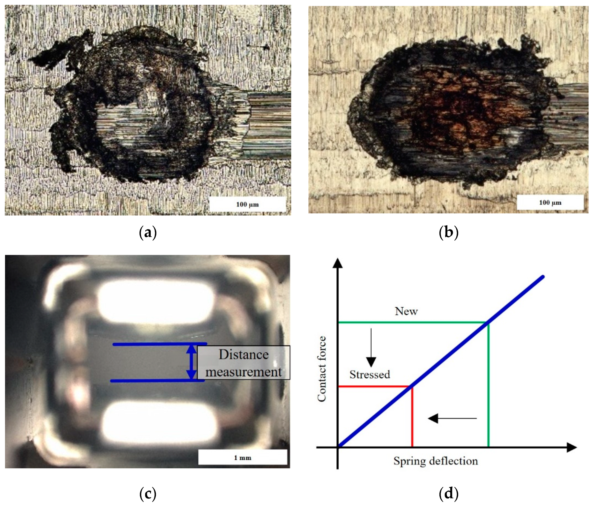
3.1. Light Microscope (LM)

A magnified image of the contact zone of electrical connectors stressed by fretting corrosion tests can be displayed by light microscopy, Figure 1a,b. This allows an initial evaluation of degradation based on visual true color representations. There is a possibility to differentiate between wear of the tin layer (Figure 1a) and the wear scars on the copper substrate (Figure 1b). The indicator of this qualitative evaluation is the black or copper-colored discolorations of the surface and the wear tracks.
Additionally, the light microscope can be used to measure the contact opening dimension of electrical contacts as a quantitative indicator for mechanical stress relaxation (Figure 1c). By measuring the contact opening dimensions of a stressed and a new electrical contact, the influence of the mechanical stress relaxation after a lifetime test can be quantitatively determined. The combination of the spring stiffness relation and the deflection of a spring element of the contact spring is shown in Figure 1d. Therefore, the contact force for a new and a stressed electrical contact can be estimated. Consequently, conclusions about thermally induced stress relaxations and the reduction of contact force can be drawn. Alternatively, CT examinations can also be used for measuring the contact opening dimension.

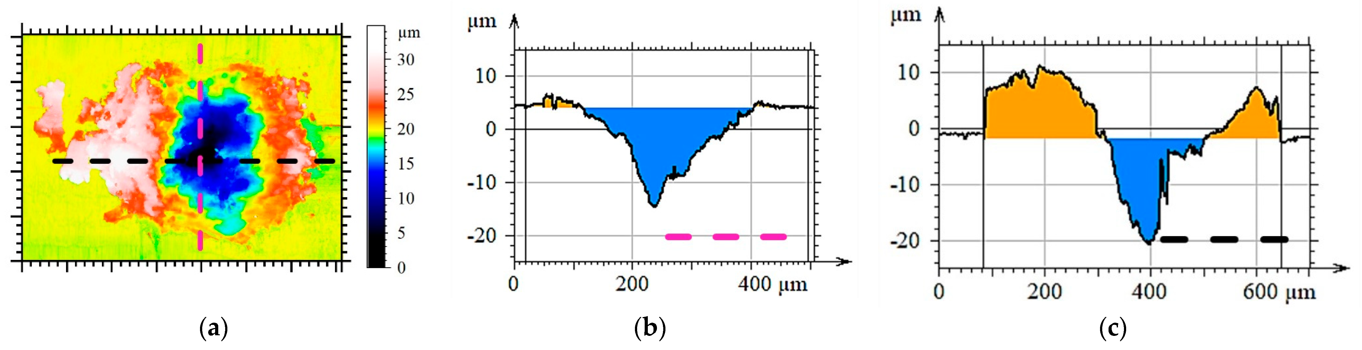
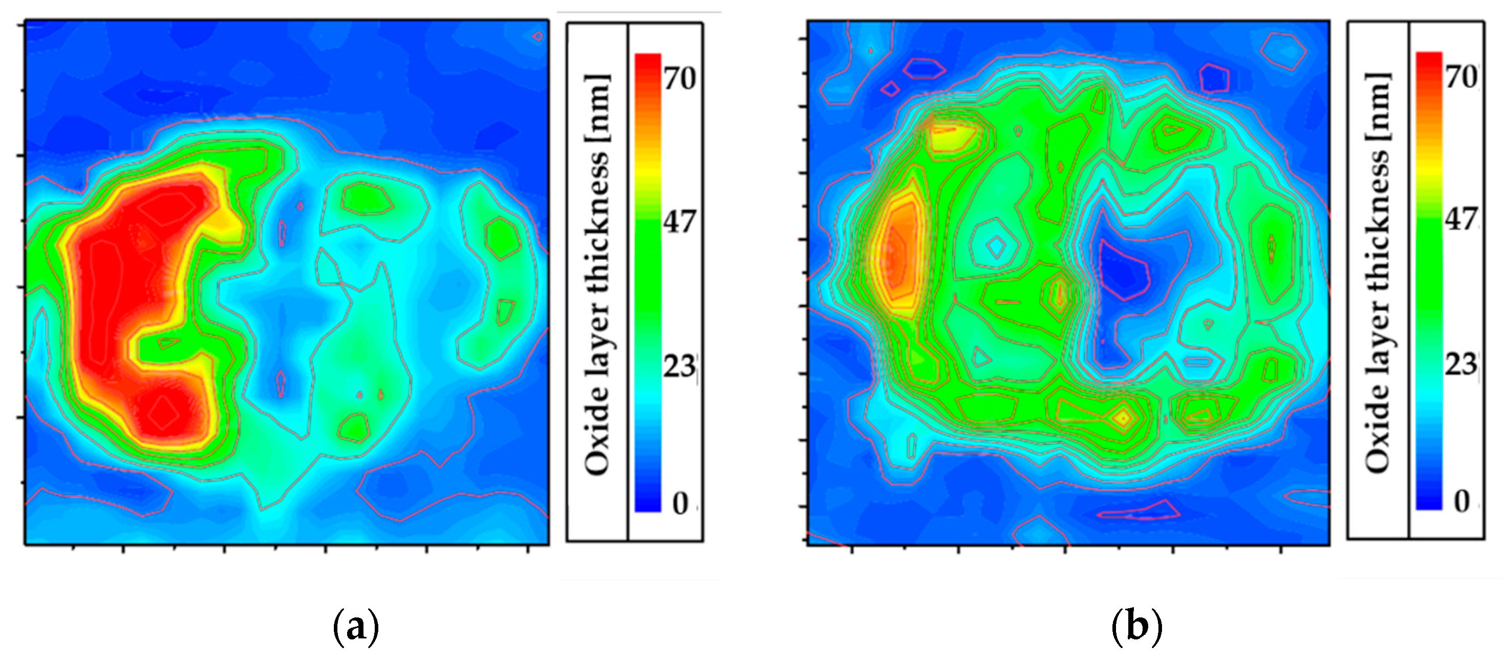
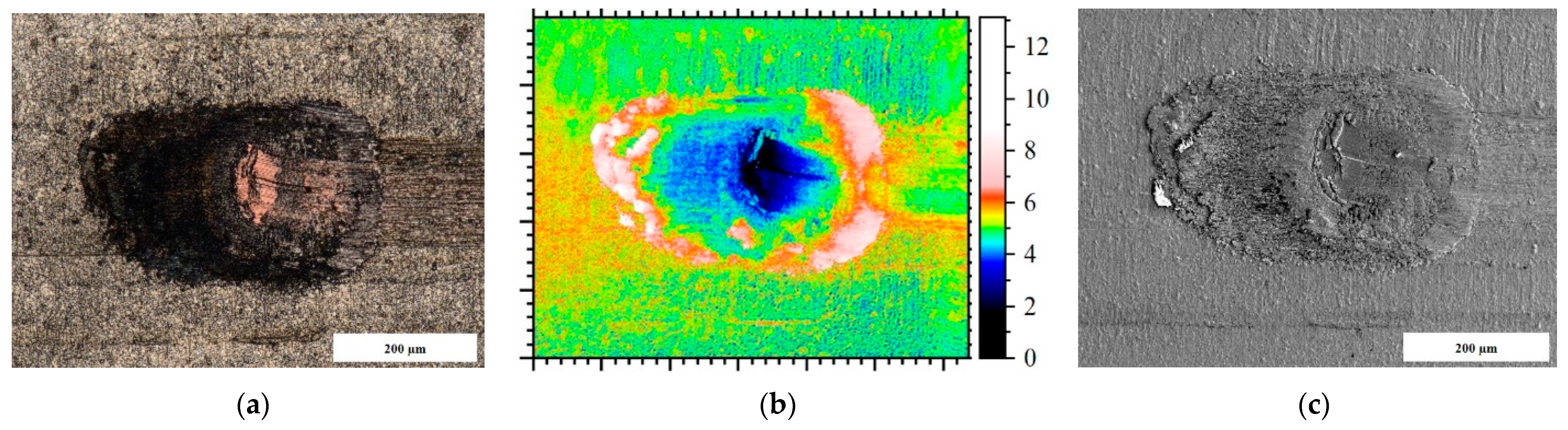
3.2. Topographic Measurement (TM)

In this study, a confocal white light microscope was used to visualize the topography of a stressed contact system. As a result, topographic surface images (Figure 2a), as well as profile lines of different directions within the contact zone, were realized, Figure 2b,c. Quantitative estimations of wear depth and volume can be made. Thus, the topography investigations show the wear of the tin coating and the agglomeration of wear particles at the edge of the contact zone. Especially for noble metals, the wear of the coating is critical.

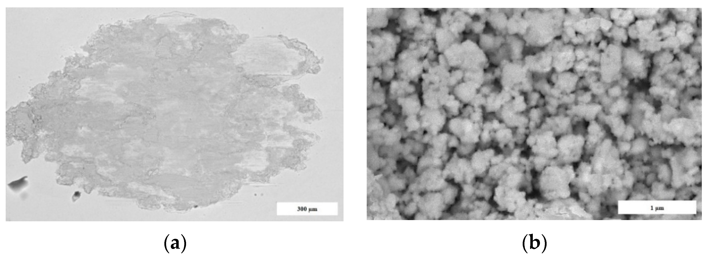
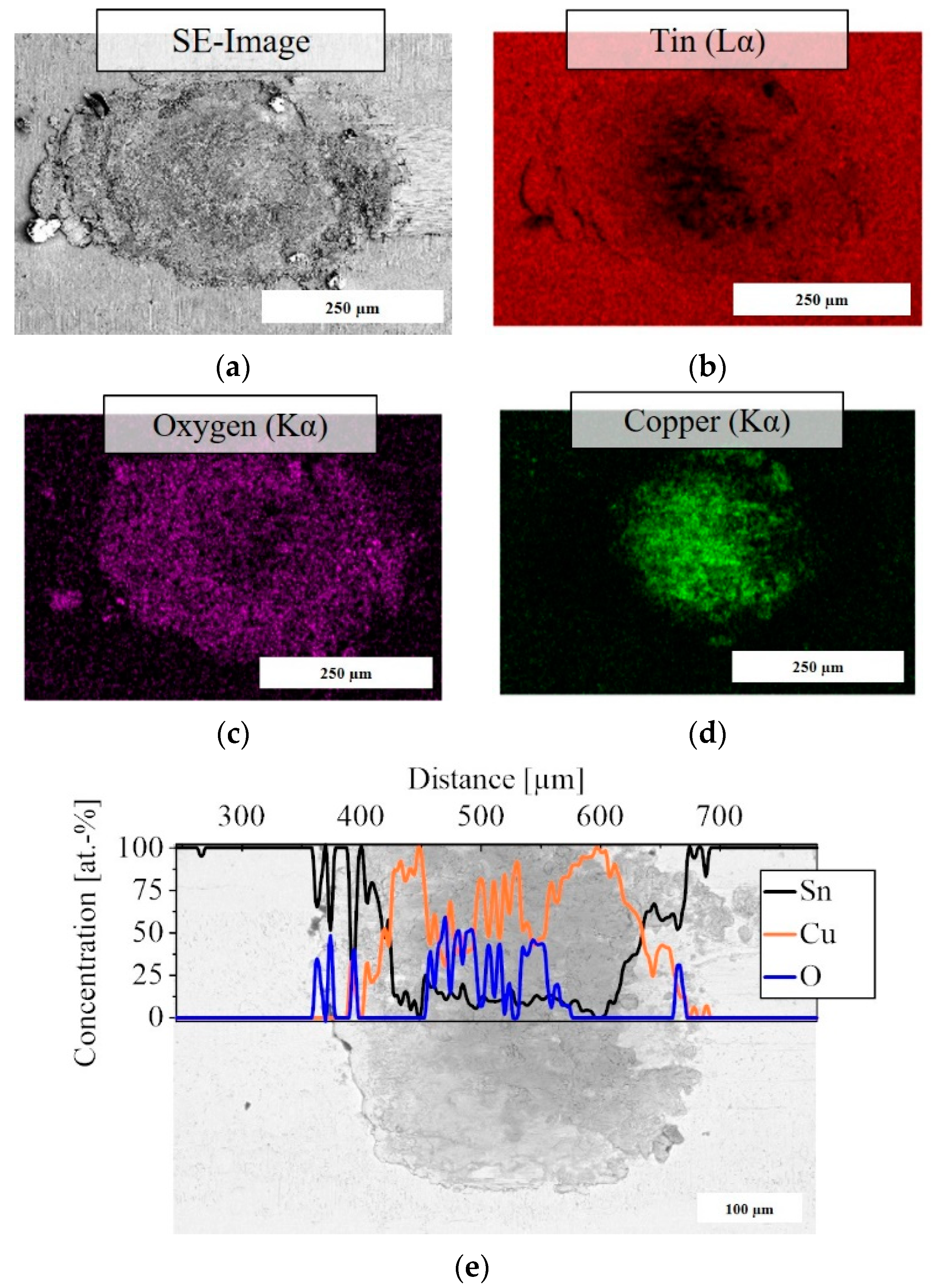
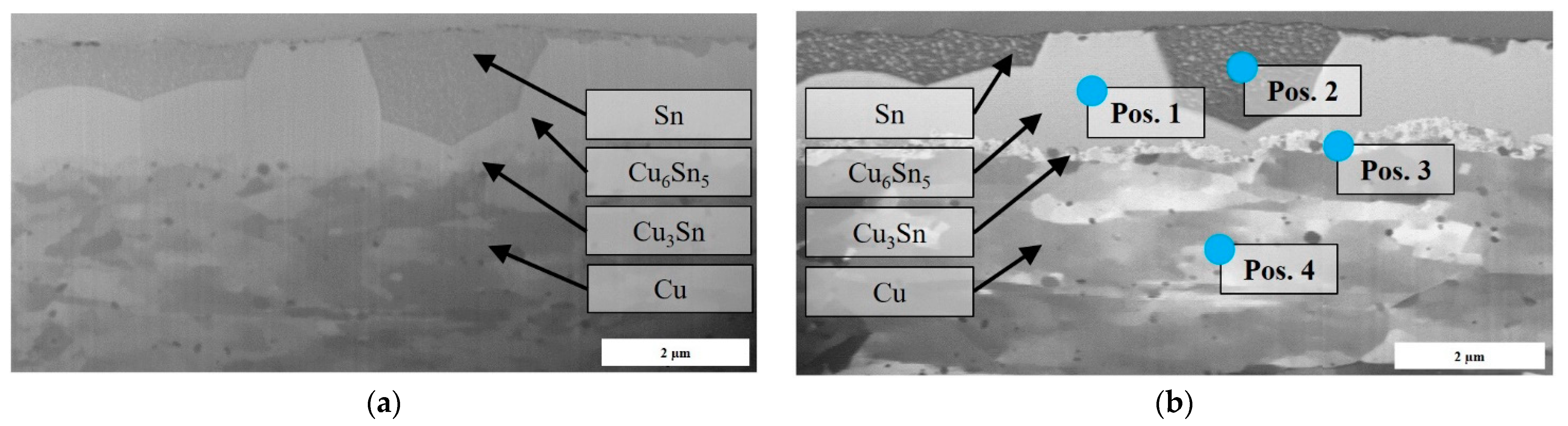
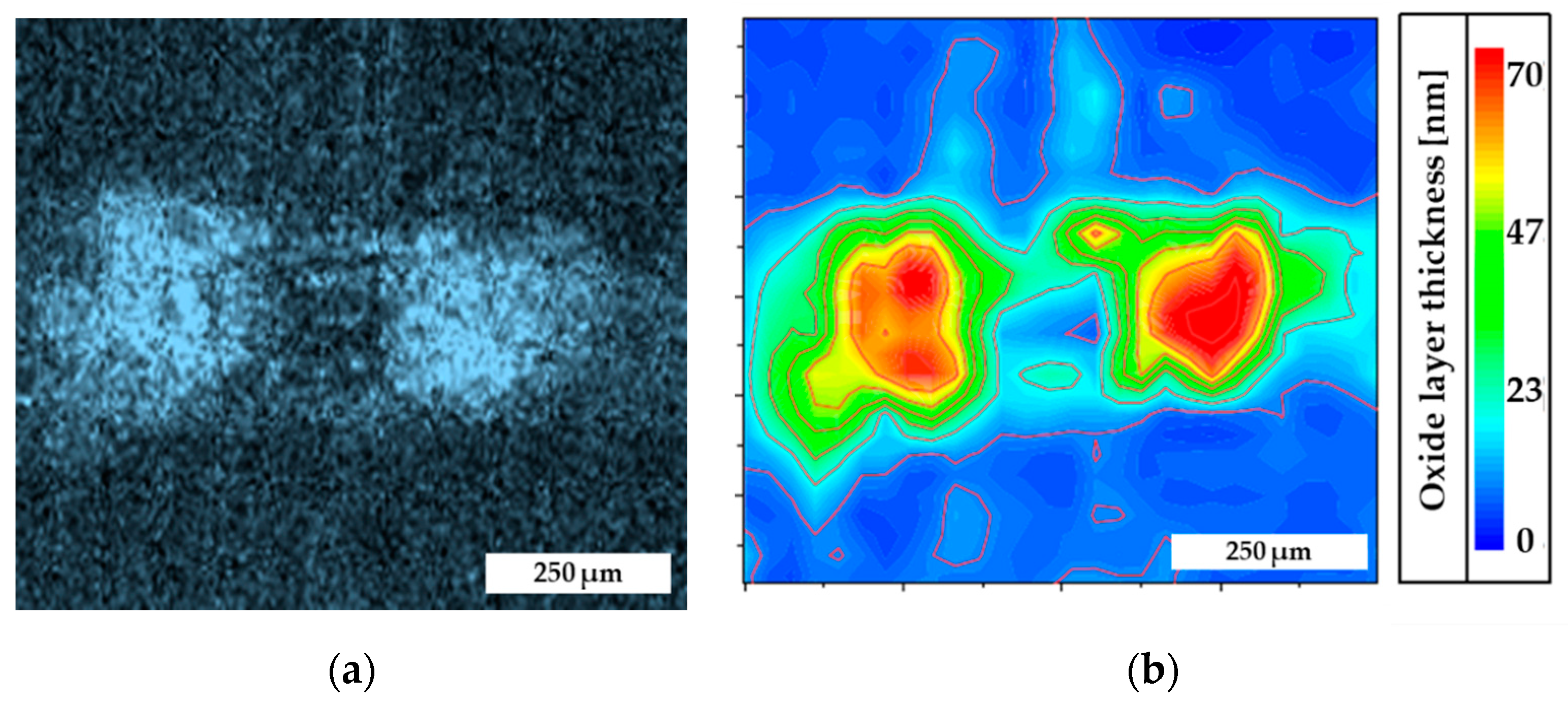
3.3. Scanning Electron Microscope (SEM) and Energy Dispersive X-ray (EDS)

A Scanning Electron Microscope is an important imaging tool used to evaluate the degradation mechanisms of electrical connectors. Especially, the high magnifications and the good depth of focus are advantageous. Figure 3a shows the wear zone of a contact after fretting corrosion test. The resulting wear particles can also be identified as a qualitative indicator of fretting corrosion, Figure 3b.
The EDS method enables the investigation of chemical elements for the evaluation of damage mechanisms. Thus, the element concentration in the wear zone of electrical connectors can be investigated qualitatively by using element mappings, Figure 4b–d, or quantitatively by a line scan, Figure 4e. The tin signal shows a reduction and an equally increased copper concentration is present. This could be due to the fact that the tin layer has been worn through by the fretting movements. Furthermore, an increased concentration of oxide has been detected. That is an indication that fretting corrosion has occurred. The advantage of element mapping is that a holistic evaluation of the contact zone is possible. However, line scanning enables locally high-precision measurements and conversions to quantitative element concentrations in atomic or mass percentage.

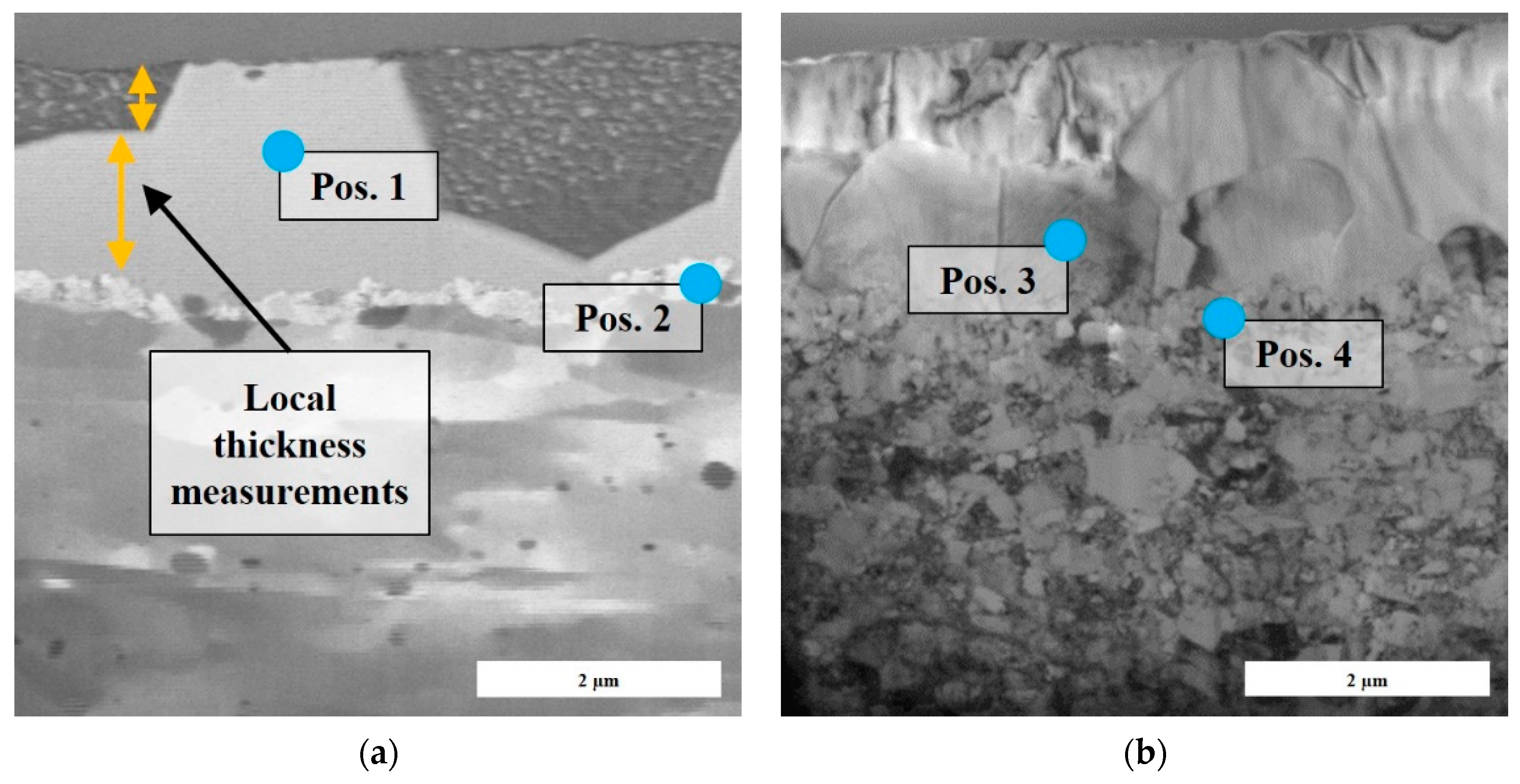
3.4. Focused-Ion-Beam (FIB)

For electrical connectors, the layer thickness and materials structure can be examined using FIB technique. By comparing the layer structures of new and stressed electrical contacts, it is possible to evaluate the diffusion processes and phase transitions induced by temperature loads. The layer thickness and material structures (size/shape of grains) are used as qualitative and quantitative indicators.
On the basis of the FIB cross-sections, an electrical connector stressed by temperature cycles is investigated by using electron beam stimulation (Figure 5a) and ion beam stimulation (Figure 5b). The layer components (Coating: Sn; Bulk: Cu; Intermetallic compounds: Cu3Sn and Cu6Sn5) become much more visible by ion beam stimulation in comparison to electron beam stimulation. The classification of the layer components was done by EDS measurements, Table 2. The element concentrations of the intermetallic compounds are comparable to the results of Braunovic [17] (p. 338). However, slight deviations of element concentrations compared to the phase diagram of tin and copper can be identified [57]. The electron and ion beams stimulate a volume of material despite the focusing during the analysis. This excited volume can rise a few micrometers into the material depending on the acceleration voltage. This could lead to slight deviations in the exact element composition. To reduce this effect, TEM analyses can be performed. However, the phases show different grain structures, which also makes a qualitative distinction for material experts possible by using this imaging tool.
Furthermore, the Cu6Sn5-layer has already grown to the top of the surface because of the temperature induced diffusions processes. Only small parts of the tin layer are left. Therefore, an increase in the electrical contact resistance due to growth of intermetallic compounds can be assumed. A comparison of the diffusion behavior at different temperatures, layer structures and substrate materials is made possible by this method.

3.5. Wavelength Dispersive X-ray (WDS)

A quantitative evaluation of the oxide debris within the wear zone of damaged electrical contacts can be carried out by using Wavelength Dispersive X-ray analysis. By means of calculations, the oxide layer thickness of the stressed electrical contacts can be quantified. This is exemplified by two different contact areas in Figure 6. The contact zones are characterized by an oxide layer thickness up to 70 nm. In the unloaded area, oxide layers of a few nanometers are identifiable. These findings are in good agreement with the study of Tamai [44]. Other contamination layers, like carbon or sulfides, can also be calculated.

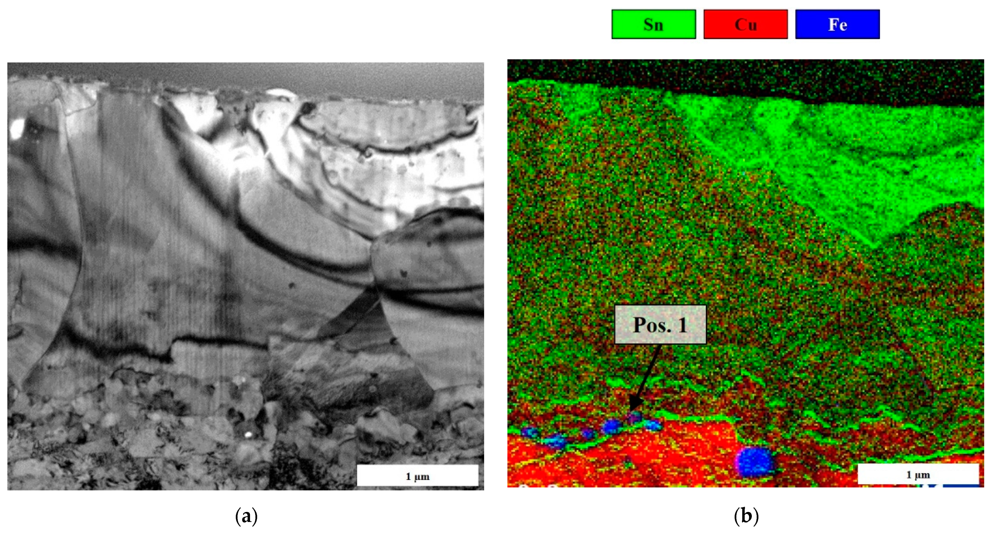
3.6. Transmission Electron Microscopy (TEM + EELS/EDS)

The possibilities of the TEM analysis on the basis of an electrical contact stressed by temperature loadings are shown in the following Figure 7. The TEM analysis shows the prepared lamella in cross-section by visualizing different material and grain structures, Figure 7a.
By means of coupled EELS measurement, chemical elements can also be assigned to the structure, Figure 7b. Thus, the tin layer, the intermetallic compounds and the copper substrate can be identified by qualitative element mappings. However, iron dispersions are located at the phase boundaries of the base material to the intermetallic compounds (Position 1). These iron dispersions are related to the alloy type and can be responsible for increasing stiffness.

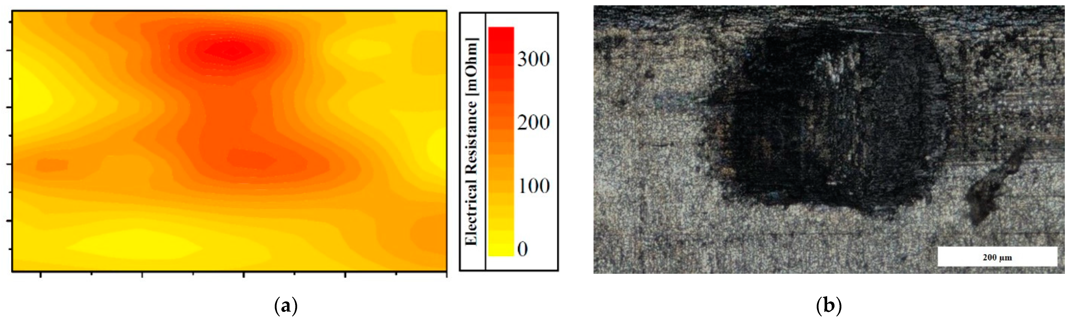
3.7. Contact Resistance Measurements and Mapping (CM)

The result of an electrical resistance mapping in an electrical contact stressed by fretting corrosion is shown in Figure 8. The electrical contact resistance is increased (Figure 8a) within the degraded contact zone (Figure 8b). Outside the contact zone, a low resistance can be observed. Thus, the observed resistance distribution is an indicator of fretting corrosion. The implementation of this method is useful when the contact resistance in a connector is unstable which could be due to the localized oxide zones within the contact area. The extent of degradation due to small pockets of oxides in the contact area are, at times, not visible and also not clear from the measured contact resistance. In such cases, contact resistance mapping can be applied to identify the extent of degradation.

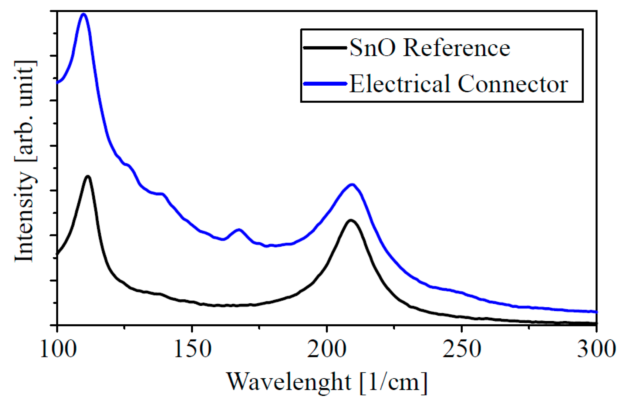
3.8. Raman Spectroscopy (RS)

Raman Spectroscopy was also used in this study to determine the oxides formed on the surface of an electrical connector. First, a tin monoxide was measured as a reference powder and compared with a measurement of a stressed contact system, Figure 9. The results show that there are commonalities between the stressed contact system and the reference powder. Therefore, tin monoxide is present in the wear zone of electrical connectors stressed by vibrations and temperature cycling tests. However, other Raman signals can also be detected. Further contamination products could also be present on the surface. That is not discussed in this study.

4. Discussion

In this section, the different methods of material and surface analysis are compared and discussed with regard to practicability in relation to different modes of failure. Following, the various analytical methods are evaluated comparatively.

4.1. Comparison of Analytical Methods

4.1.1. Methods for Visualizing the Surface

In the first step, the imaging methods LM, TM and SEM for visualization of the surface are compared, Figure 10. FIB and TEM analyses are also imaging methods, whereby, these are used to examine the material structure in cross-section and are later considered separately.
Generally, the imaging methods provide qualitative and quantitative indicators that allow an evaluation of the degradation mechanism. Particularly, for LM, the true color representation is important, as it is the only analysis tool that shows dark discoloration caused by fretting corrosion or abrasion on the copper substrate visually in true colors, Figure 10a. Topography measurement is also an imaging method, whereby, it only takes into account the topography and cannot represent true colors, Figure 10b. Through this, quantitative estimation of wear can be obtained.
The SEM cannot display colors either, Figure 10c. However, the various visualizations of topography and material contrast by detecting different electrons, as well as the high resolution of SEM, are useful for visualizing oxide particles, cracks or microscopic delamination. The other imaging methods (LM and TM) do not achieve the required resolution for the visualizing of wear particles. This is only possible by using the SEM. The optical examination methods are non-destructive in nature.

4.1.2. Methods for Validation of Mechanical Stress Relaxation

Temperature-induced changes in the contact opening dimensions of the contact springs due to mechanical stress relaxation can be investigated by two methods. This includes LM and CT analyses. In particular, the simple handling and the fast procedure make the LM attractive. Although CT analyses can provide further information about the contact design, they are also associated with increased analysis and evaluation effort.

4.1.3. Methods for Analyses of Chemical Composition

In practice, the determination of the element composition of materials and surfaces is possible by various methods. These include EDS, WDS, RS, as well as AES and XPS. The oxide mappings of a degraded contact zone are represented by EDS (qualitative) in Figure 11a and WDS (quantitative) in Figure 11b. By means of EDS and WDS analyses, the elements are determined on the basis of X-rays. The differences between WDS and EDS are the analytical evaluation and the quantification of the geometric layer thicknesses. Nevertheless, the EDS method is one of the simplest and fastest analysis methods for element investigations and is often used in practice. AES and XPS analyses determine the element composition on the surface with a depth resolution of a few nanometers. Therefore, these methods are extremely surface-sensitive. The RS is suitable for the analysis of different materials structure and composition. Local mappings are also possible, but the interpretation is highly complex. Additionally, the chemical analysis methods are non-destructive.

4.1.4. Methods for Visualizing of the Layers and Material Structure

For detection of the material and layer structure, the imaging methods of FIB and TEM analysis can be used. Both allow qualitative indicators by the evaluation of the image. Figure 12 shows the comparison of the layer structure of an electrical connector by FIB and TEM analysis combined with chemical analysis in Table 3.
The FIB analysis represents the different layer structures by ion beam stimulation with a sufficient contrast in Figure 12a. Thus, a qualitative differentiation of the different components of layer components is possible. In the TEM, there is also a differentiation between substrate and coating feasible, Figure 12b. The contrast is not sufficient for the clear distinction of the interface between intermetallic compounds and base or coating metals. However, the grain and microstructure of the materials and coatings are pronounced. Both methods allow quantitative analyses by geometric measurements of the layer thicknesses or the combination with chemical analysis methods such as EDS, Figure 12 and Table 3.
Thus, the identification of intermetallic compounds with the chemical investigation of the element composition is possible by using both methods. However, the additional EDS analysis shows that the element concentrations have slight differences, Table 3. This is due to the fact that the TEM has a much lower stimulation volume due to the penetration of a thin lamella than by FIB analyses. Thus, quantitative elemental analyses by the TEM are more detailed, as there are fewer scattering effects due to the excited volume. This is also illustrated by the fact that determined element concentrations of the intermetallic phases have a higher accuracy to the literature of the phase diagram of Fürtauer [57]. However, FIB and TEM are destructive analytical tools.

4.1.5. Methods for Electrical Investigations

In principle, surfaces can be electrically characterized by Atomic Force Microscope (AFM). However, this is considered unsuitable for the application of electrical connectors due to surface roughness and experimental boundary conditions. Therefore, the CM is the only method specified to characterize the surface locale resolved electrically. Nevertheless, it is also recommended to measure the contact resistance of an electrical connector in the contacted state.

4.2. Validation of the Methods

Each method is evaluated concerning to the availability and effort to execute, as well as the required expertise for interpretation of the results in Table 4. The availability is also correlated with the results of Section 2. Light Microscopy and Topography Measurements are widely used methods, whereby, low expert knowledge is required for the implementation and interpretation. SEM, EDS and FIB are applied in combinatorial analytics. In particular, the required expertise estimated is higher due to the more complex physical principles than that for Light Microscopy. The measurements of Contact Resistance Mappings also require medium expertise, whereby, the availability is rated lower than for SEM analysis.
CT, RS, AES, XPS, TEM and WDS are special analytical methods. These are used very rarely due to low availability and high effort. Furthermore, the required expert knowledge for the implementation and interpretation of these analyses is much higher. The complex physical principles are responsible for that. In addition to availability and the required expertise of the users, the application of such methods must also be considered in terms of the duration and the costs of the analysis. However, this cannot be evaluated in general, as this is dependent on the respective questions and the detail of the analysis.
In Table 5, the surface analytical methods are presented with regard to their applicability for the investigation of different modes of failure for electrical connectors. Fretting corrosion is due to a combination of wear and corrosion processes caused by relative motions. This is especially critical for non-noble coatings. The degradation mechanisms of fretting wear are based on relative motions, as well. However, for noble surface materials, the wear process and wear through of the coating is critical. By uncovering the non-noble base material, fretting corrosion occurs. The mechanism of relaxation is considered as mechanical stress relaxation as a result of operation at high temperatures. Oxidation and corrosion include chemical processes caused by the atmosphere or corrosive gases without a tribological load. Other surface damages include the growth of the intermetallic compounds, crystallization effects, structural phase transformations and other surface and material effects.
Light Microscopy is an elementary method for the analysis due to the representation of true colors with acceptable magnifications and the diverse applications. Topographic analysis by measurement of the surface geometry is suitable to investigate fretting corrosion and fretting wear of functional layers. Other degradation mechanisms cannot be investigated with this method. By investigation using SEM, high-resolution images of the surface with high magnification can be realized. Complementary chemical analyses using EDS make it possible to identify various contamination products. For fast and easy chemical analysis, EDS is preferable to WDS due to the ease of use. However, WDS has a very high energy resolution. Low element concentrations can be investigated by WDS in a better way than by EDS. FIB investigations are used for the investigation of specific failure modes by analyzing the material and the layer structure by local cross sections. Diffusion processes and phase changes caused by temperature influences can also be analyzed by FIB. However, the crucial property of electrical connectors is the contact resistance. Electrical resistance mapping is a valid method to electrically characterize the surfaces of electrical contacts after a qualification test. Especially if a measurement of the electrical contact resistance in the contacted state is not possible, contact resistance mapping is a possibility to examine the surface electrically. Furthermore, resistance changes due to phase transformations as a result of diffusion processes can also be quantified.
Raman Spectroscopy can be used as a further analysis method to investigate oxidation and corrosion processes for fretting corrosion, as well as for other surface contaminations. The use of RS for electrical connectors is only recommended for specific investigations. Furthermore, AES, XPS and TEM examinations are also methods that should only be used in exceptional cases due to the high effort and the enormous complexity. This is also reflected in the fact that the range of applications is limited in terms of the reasonable use for the mode of failures.

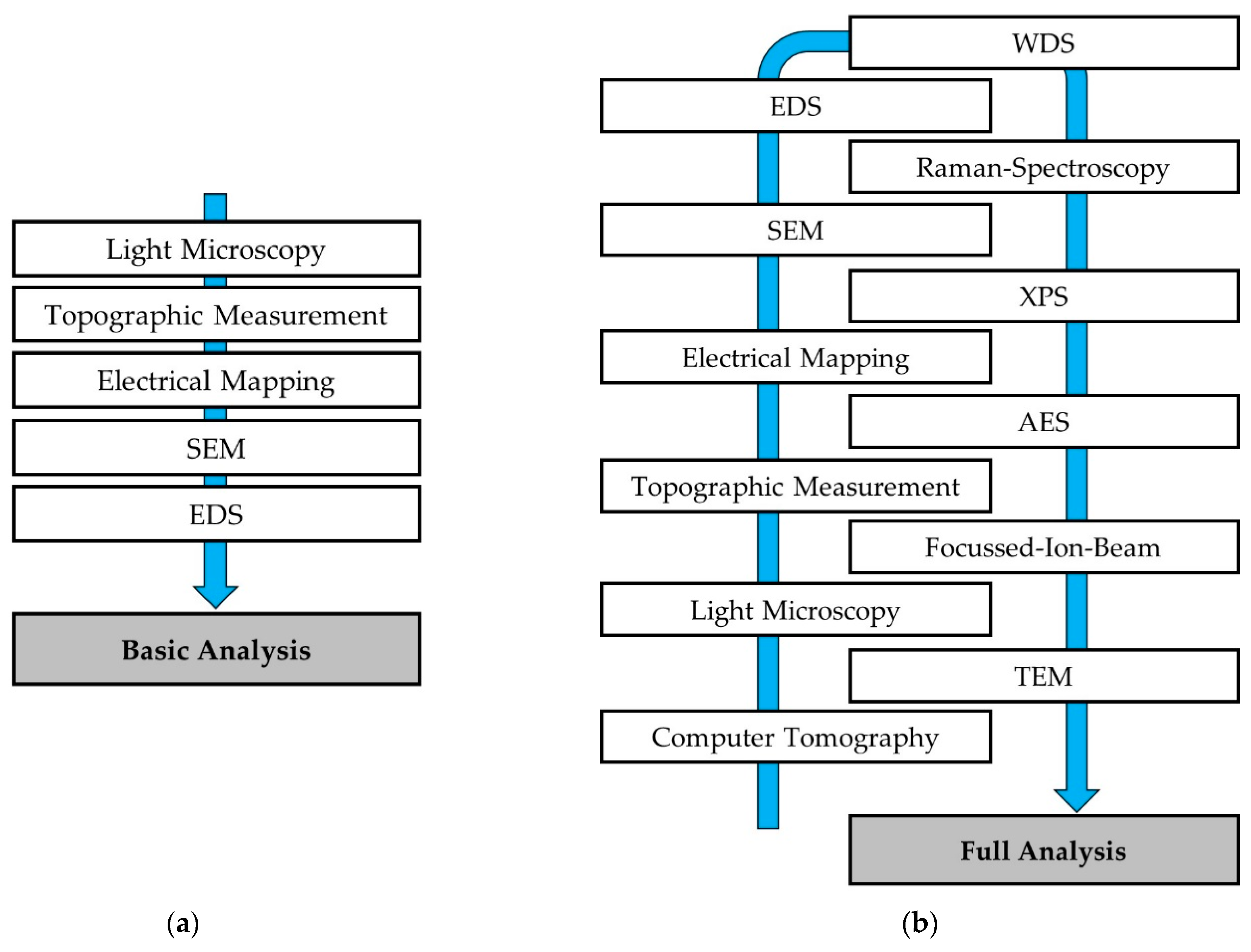
4.3. Analysis Workflow

Based on the investigations of this study, recommendations for an efficient workflow for analyzing causes of failure for electrical connectors are presented. However, a distinction is made between a fast basic analysis and a more complex, as well as time-consuming and financially intensive, analysis.
The basic analysis consists of five methods, which provide the most comprehensive information of the examined component, Figure 13a. These include Light Microscope, Topographic Measurements, Contact Resistance Mappings, SEM and EDS. Light Microscopy is suitable for an initial visual validation and documentation of possible failure modes, such as fretting corrosion, wear or other surface related degradations. Topography measurements can be used to quantify degradations such as wear-through of the coating. In addition, an imaging analysis with chemical investigations is possible by using SEM and EDS. Thus, oxides or particle contaminants on the surfaces of the contacts can be chemically identified. The electrical effects of such failure modes can finally be determined with contact resistance mapping. This allows the contact systems to be effectively examined for the most important failure modes. This also correlates with the analysis of the methods used in the literature (Section 2).
A comprehensive analysis is supplemented by other methods and can provide further information about oxide compounds, contamination layer thicknesses or microstructure of materials. This analysis process is shown in Figure 13b. The additional methods presented in the comprehensive analysis offer possibilities to investigate failure modes in more detail. However, the information derived through their application is rarely needed for the reliable analysis of electrical connectors.
The steps of the workflow can vary depending on the component and the specific problem. Likewise, this methodology can also be applied to other contact surfaces (noble coatings like gold or silver), whereby, the analyses should be directed with the focus to the correlated cause of failures for those surfaces.

5. Conclusions

This study deals with various methods of material and surface analysis for the investigation and evaluation of the lifetime and reliability of electrical connectors. In general, the lifetime of electrical contacts is influenced by various modes of failure. For investigation of those failure modes, a wide variety of analytical methods are used in research, whereby, not every method can be applied reasonably for each cause of failure.
Analytical results of various methods were discussed for tin coated electrical connectors. In particular, a focus of this study was placed on the practicability of investigation of various modes of failures, as well as the availability and the required expertise for implementation and evaluation of results. An analysis of stressed electrical contacts by Light Microscopy, Topographic Measurements, SEM, EDS and Contact Resistance Mappings can provide valuable information for determining the cause of failure.
Other methods, such as Raman Spectroscopy or TEM analyses, offer further insights into special topics. Furthermore, the exemplary results show the influence on the reliability of electrical contacts stressed by different tests. The study provides recommendations for an efficient and effective approach for analysis of failure modes of electrical contacts.
The results, opinions and conclusions expressed in this publication are not necessarily those of Volkswagen Aktiengesellschaft.

Author Contributions

Conceptualization, P.K. and J.S.; methodology, P.K. and J.S.; validation, P.K. and J.S.; formal analysis, P.K.; investigation, P.K.; writing—original draft preparation, P.K.; writing—review and editing, A.S. and J.S.; visualization, P.K.; supervision, J.S. All authors have read and agreed to the published version of the manuscript.

Funding

This research received no external funding.

Institutional Review Board Statement

Not applicable.

Informed Consent Statement

Not applicable.

Data Availability Statement

Not applicable.

Conflicts of Interest

The authors declare no conflict of interest.

References

  1. Kloch, K.T.; Kozak, P.; Mlyniec, A. A review and perspectives on predicting the performance and durability of electrical contacts in automotive applications. Eng. Fail. Anal. 2021, 121, 105143. [Google Scholar] [CrossRef]
  2. Kolmer, P.; Rojer, M.; Song, J.; Schramm, D. Surface Degradation of Electrical Connectors stressed by Multivariable Lifetime Tests. In Proceedings of the 66th IEEE Holm Conference on Electrical Contacts, San Antonio, TX, USA, 24–27 October 2021; pp. 149–158. [Google Scholar] [CrossRef]
  3. Song, J.; Yuan, H.; Koch, C. Accelerated Testing of Electromechanical Connectors Considering Thermal and Mechanical Loads. In Proceedings of the 64th IEEE Holm Conference on Electrical Contacts, Albuquerque, NM, USA, 14–18 October 2018; pp. 467–474. [Google Scholar] [CrossRef]
  4. Hilmert, D.; Krüger, K.; Song, J. Vergleichende Untersuchung der Verschleißbilder von Steckverbindern aus Reibverschleiß- und Vibrationsprüfungen mit unterschiedlichen Prüfrichtungen. In Proceedings of the 62nd German Tribology Conference (62. Tribologie-Fachtagung), Online, Germany, 27–29 September 2021; pp. 52/1–52/10. [Google Scholar]
  5. Reif, K. Batterien, Bordnetze und Vernetzung, 1st ed.; Vieweg+Teubner Verlag: Wiesbaden, Germany, 2010; p. 33. [Google Scholar]
  6. Swingler, J.; McBride, J.W.; Maul, C. Degradation of road tested automotive connectors. IEEE Trans. Compon. Packag. Technol. 2000, 23, 157–164. [Google Scholar] [CrossRef]
  7. Schautzgy, J.; Ivanov, Y.; Kröger, B.; Wilde, J. Durability studies on vibration-loaded electrical contact systems subjected to tribological stress. Mater. Test. 2019, 61, 105–110. [Google Scholar] [CrossRef]
  8. Kolmer, P.; Song, J.; Schramm, D. Oberflächenanalytische Untersuchungen an elektrischen Steckkontakten. In Proceedings of the 8th Symposium Connectors (Elektrische und optische Verbindungstechnik), Online, Germany, 23–24 March 2021; pp. 134–144. [Google Scholar]
  9. Schmidt, H.; Buresch, I.; Stokowski, A. Alterungsmechanismen bei Steckverbindern, die nicht Arrhenius-Zusammenhängen gehorchen. In Proceedings of the 25th Albert-Keil-Conference (Kontaktverhalten und Schalten), Karlsruhe, Germany, 9–11 October 2019; pp. 74–84. [Google Scholar]
  10. Buresch, I.; Rehbein, P.; Klaffke, D. Possibilities of Fretting Corrosion Model Testing for Contact Surfaces of Automotive Connectors. In Proceedings of the 2nd World Tribology Congress, Vienna, Austria, 3–7 September 2001; pp. 413–416. [Google Scholar]
  11. ZVEI—Zentralverband der Elektrotechnik und Elektronikindustrie e.V. Technischer Leitfaden—TLF 0214 Validierung von Automotive-Niedervolt-Steckverbindern. Available online: https://www.zvei.org/presse-medien/publikationen/technischer-leitfaden-tlf-0214-validierung-von-automotive-niedervolt-steckverbindern (accessed on 14 October 2021).
  12. Dörnhöfer, A. Betriebsfestigkeitsanalyse Elektrifizierter Fahrzeuge—Multilevel-Ansätze zur Absicherung von HV-Batterien und Elektrischen Steckkontakten, 1st ed.; Springer Vieweg: Berlin, Germany, 2019. [Google Scholar] [CrossRef]
  13. Bauch, J.; Rosenkranz, R. Physikalische Werkstoffdiagnostik, Ein Kompendium wichtiger Analytikmethoden für Ingenieure und Physiker, 1st ed.; Springer Vieweg: Berlin, Germany, 2017. [Google Scholar] [CrossRef]
  14. Song, J.; Yuan, H.; Shukla, A.; Koch, C.; Hilmert, D. Correlation of Connector Contact Failures in Accelerated Testing and in Long-term Use Field Vehicles. In Proceedings of the 65th IEEE Holm Conference on Electrical Contacts, Milwaukee, WI, USA, 14–18 September 2019; pp. 296–302. [Google Scholar] [CrossRef]
  15. Wielsch, T.; Ostendorf, F.; Reiniger, M. Lebensdauer- und Zuverlässigkeitsvorhersage von Steckverbinderkontakten. In Proceedings of the 4th Symposium Connectors (Elektrische und optische Verbindungstechnik), Lemgo, Germany, 6–7 March 2013; pp. 228–250. [Google Scholar]
  16. Ostendorf, F.; Wielsch, T.; Reiniger, M. Reliability assessment and field failure predictions—A prognostic model for separable electrical contacts. In Proceedings of the 27th International Conference on Electrical Contacts, Dresden, Germany, 22–26 June 2014; pp. 278–283. [Google Scholar]
  17. Braunovic, M.; Konchits, V.V.; Myshkin, N.K. Electrical Contacts: Fundamentals, Applications and Technology, 1st ed.; Taylor & Francis Group: Boca Raton, FL, USA, 2006. [Google Scholar]
  18. Braunovic, M. Fretting in Electrical/Electronic Connections: A Review. IEICE Trans. Electron. 2006, E92-C, 982–991. [Google Scholar] [CrossRef]
  19. Slade, P.G. Electrical Contacts: Principles and Applications, 2nd ed.; Taylor & Francis Group: Boca Raton, FL, USA, 2014. [Google Scholar]
  20. Vinaricky, E.; Schröder, K.H.; Weiser, J. Elektrische Kontakte, Werkstoffe und Anwendungen: Grundlagen, Technologien, Prüfverfahren, 3rd ed.; Springer Vieweg: Berlin, Germany, 2016. [Google Scholar] [CrossRef]
  21. Song, J.; Schinow, V.; Yuan, H. Third bodies in electrical contacts—Wear and electrical performance. In Proceedings of the 63rd IEEE Holm Conference on Electrical Contacts, Denver, CO, USA, 10–13 September 2017; pp. 117–124. [Google Scholar] [CrossRef]
  22. Munoz, A.I.; Espallargas, N.; Mischler, S. Tribocorrosion, 1st ed.; Springer: Cham, Switzerland, 2020; p. 1. [Google Scholar] [CrossRef]
  23. Gao, J.; Chen, C.; Flower, G.T.; Jackson, R.L.; Bozack, M.J. The Influence of Particulate Contaminants on Vibration-Induced Fretting Degradation in Electrical Connectors. In Proceedings of the 56th IEEE Holm Conference on Electrical Contacts, Charleston, SC, USA, 4–7 October 2010; pp. 108–112. [Google Scholar] [CrossRef]
  24. Kong, Z.; Swingler, J. Combined effects of fretting and pollutant particles on the contact resistance of the electrical connectors. Prog. Nat. Sci.: Mater. Int. 2017, 27, 385–390. [Google Scholar] [CrossRef]
  25. Ghaednia, H.; Jackson, R.L.; Gao, J. A third body contact model for particle contaminated electrical contacts. In Proceedings of the 60th IEEE Holm Conference on Electrical Contacts, New Orleans, LA, USA, 12–15 October 2014; pp. 24–28. [Google Scholar] [CrossRef]
  26. Hilmert, D.; Yuan, H.; Song, J. The Analysis of Failure Mechanisms of Electrical Connectors in Long-term Use Field Vehicles. In Proceedings of the 67th IEEE Holm Conference on Electrical Contacts, Tampa, FL, USA, 23–26 October 2022; pp. 1–8. [Google Scholar]
  27. Yuan, H.; Song, J. Fretting Corrosion Behavior of Various Contact Surfaces under Diverse Operating Conditions. In Proceedings of the 65th IEEE Holm Conference on Electrical Contacts, Milwaukee, WI, USA, 14–18 September 2019; pp. 19–26. [Google Scholar] [CrossRef]
  28. Buresch, I. Effekte intermetallischer Phasen auf die Eigenschaften von Zinnoberflächen auf Kupferlegierungen. In Proceedings of the 21st Albert-Keil-Conference (Kontaktverhalten und Schalten), Karlsruhe, Germany, 29–30 September 2011; pp. 38–46. [Google Scholar]
  29. Sachs, S.; Schmidt, H. Untersuchung lokaler Kontaktwiderstände durch Rastersonden-Mikro-Abtastung von Kontaktoberflächen. In Proceedings of the 8th Symposium Connectors (Elektrische und optische Verbindungstechnik), Online, Germany, 23–24 March 2021; pp. 184–192. [Google Scholar]
  30. Fili, T.; Ospeld, T.; Hottes, M.; Günther, J. Bewertung von Kontaktoberflächen nach Qualifikationstests–Unterschiede in Aussage und Methode zwischen Gold, Silber und Zinn. In Proceedings of the 6th Symposium Connectors (Elektrische und optische Verbindungstechnik), Lemgo, Germany, 15–16 March 2017; pp. 100–114. [Google Scholar]
  31. Yuan, H.; Hilmert, D.; Shukla, A.; Song, J. Effect of Direction on Fretting Corrosion Behaviour. In Proceedings of the 66th IEEE Holm Conference on Electrical Contacts, San Antonio, TX, USA, 24–27 October 2021; pp. 38–45. [Google Scholar] [CrossRef]
  32. Song, J.; Yuan, H.; Schinow, V. Fretting corrosion behavior of electrical contacts with tin coating in atmosphere and vacuum. Wear 2019, 426–427, 1439–1445. [Google Scholar] [CrossRef]
  33. Pompanon, F.; Fouvry, S.; Alquier, O. Influence of humidity on the endurance of silver-plated electrical contacts subjected to fretting wear. Surf. Coat. Technol. 2018, 354, 246–256. [Google Scholar] [CrossRef]
  34. Yuan, H.; Song, J. An Improved Calculation Model for the Prediction of the Wear of Coated Electrical Contacts. Technologies 2019, 7, 77. [Google Scholar] [CrossRef] [Green Version]
  35. Yuan, H.; Song, J.; Schinow, V. Fretting Corrosion of Tin Coated Electrical Contacts: The Influence of Normal Force, Coating Thickness and Geometry of Sample Configuration. In Proceedings of the 62nd IEEE Holm Conference on Electrical Contacts, Clearwater Beach, FL, USA, 9–12 October 2016; pp. 33–38. [Google Scholar] [CrossRef]
  36. Sung, I.H.; Kim, J.W.; Hoh, H.J.; Jang, H. Effect of displacement and humidity on contact resistance of copper electrical contacts. Tribol. Int. 2016, 95, 256–261. [Google Scholar] [CrossRef]
  37. Trinh, K.E.; Mücklich, F.; Ramos-Moore, E. The role of microstructure and surface topography in the electrical behavior of Sn-coated Cu contacts. In Proceedings of the 27th International Conference on Electrical Contacts, Dresden, Germany, 22–26 June 2014; pp. 243–248. [Google Scholar]
  38. Park, Y.W.; Ramesh Bapu, G.N.K.; Lee, K.Y. The influence of current load on fretting of electrical contacts. Tribol. Int. 2009, 42, 682–689. [Google Scholar] [CrossRef]
  39. Park, Y.W.; Sankara Narayanan, T.S.N.; Lee, K.Y. Effect of temperature on the fretting corrosion of tin plated copper alloy contacts. Wear 2007, 262, 320–330. [Google Scholar] [CrossRef]
  40. Park, Y.W.; Ramesh Bapu, G.N.K.; Lee, K.Y. Fretting corrosion characteristics of electrodeposited and hot dipped tin coatings contacts. Surf. Coat. Technol. 2008, 202, 3164–3174. [Google Scholar] [CrossRef]
  41. Kondo, T.; Nakata, H.; Sekikawa, J.; Kubota, Y.; Hayakawa, K.; Nakamura, T. An analysis of relationship between contact resistance and fracture of oxide film for connector contacts using finite element method. In Proceedings of the 60th IEEE Holm Conference on Electrical Contacts, New Orleans, LA, USA, 12–15 October 2014; pp. 73–78. [Google Scholar] [CrossRef]
  42. Leidner, M.; Thoss, S.; Schmidt, H.; Reinert, L.; Trinh, K.; Schäfer, C.; Mücklich, F. Verbesserung der tribologischen und elektrischen Eigenschaften von Zinn-Kontaktoberflächen durch Partikel/Schmierstoff-Einbettung mittels Laser-Texturierung. In Proceedings of the 6th Symposium Connectors (Elektrische und optische Verbindungstechnik), Lemgo, Germany, 15–16 March 2017; pp. 59–67. [Google Scholar]
  43. Kim, M.J.; Kim, H.K. Effects of temperature and span amplitude on fretting corrosion behavior of tin-plated electrical contacts. Microelectron. Reliab. 2017, 69, 80–87. [Google Scholar] [CrossRef]
  44. Tamai, T.; Nabeta, Y.; Sawada, S.; Hattori, Y. Property of Tin Oxide Film Formed on Tin-Plated Connector Contacts. In Proceedings of the 56th IEEE Holm Conference on Electrical Contacts, Charleston, SC, USA, 4–7 October 2010; pp. 295–302. [Google Scholar] [CrossRef]
  45. Mashimo, K.; Shimoyamada, A.; Sasaki, H. Contact Resistance Prediction from Observed Image and Oxide Volume Analysis. In Proceedings of the 66th IEEE Holm Conference on Electrical Contacts, San Antonio, TX, USA, 24–27 October 2021; pp. 46–50. [Google Scholar] [CrossRef]
  46. Müller, K.; Getto, R.; Nowottnick, M. Charakterisierung von ODT auf technischen Silberoberflächen für Steckverbinder. In Proceedings of the 6th Symposium Connectors (Elektrische und optische Verbindungstechnik), Lemgo, Germany, 15–16 March 2017; pp. 80–90. [Google Scholar]
  47. Buresch, I. Yellowishing of Tin Coatings at elevated Temperatures. In Proceedings of the 27th International Conference on Electrical Contacts, Dresden, Germany, 22–26 June 2014; pp. 175–180. [Google Scholar]
  48. Mashimo, K.; Hori, Y.; Yamazaki, S. A XANES Study of Natural Oxide Films on Plated Tin. In Proceedings of the 64th IEEE Holm Conference on Electrical Contacts, Albuquerque, NM, USA, 14–18 October 2018; pp. 130–134. [Google Scholar] [CrossRef]
  49. Czichos, H.; Habig, K.H. Tribologie-Handbuch, 3rd ed.; Vieweg + Teubner: Wiesbaden, Germany, 2010; p. 211. [Google Scholar]
  50. Wohlschlögel, T.; Kaloudis, M. Praktische Oberflächenanalytik—Überblick über die Verfahren EDX, AES, XPS und SIMS. PLUS Prod. Von Leit. Und Syst. 2012, 14, 343–352. [Google Scholar]
  51. Willich, P.; Schiffmann, K.; Bethke, R. Elektronenstrahl-Mikroanalyse zur Charakterisierung dünner Schichten. Dünne Schichten 1993, 4, 44–47. [Google Scholar]
  52. Schiffmann, K.; Steinberg, C. EPMA-Analyse dünner PVD- und CVD-Schichten. Vak. Prax. Und Forsch. 2019, 31, 26–36. [Google Scholar] [CrossRef]
  53. Pouchou, J.L.; Pichoir, F. Surface Film X-ray Microanalysis. Scanning 1990, 12, 212–224. [Google Scholar] [CrossRef]
  54. Wahl, M.; Brodyanski, A.; Lösch, J.; Kopnarski, M.; Loos, P.; Beau, P.; Kolmer, P. Analytische Charakterisierung der Oberflächenkorrosion von kobaltbasierten Legierungen unter (Hoch-)Temperatur-Reibbelastung. In Proceedings of the 61st German Tribology Conference (61. Tribologie-Fachtagung), Online, Germany, 29–30 September 2020; pp. 28/1–28/10. [Google Scholar]
  55. Köver, L.; Kovacs, Z.; Sanjines, R.; Moretti, G.; Cserny, I.; Margaritondo, G.; Palinkas, J.; Adachi, H. Electronic Structure of Tin Oxides: High-resolution Study of XPS and Auger Spectra. Surf. Interface Anal. 1995, 23, 461–466. [Google Scholar] [CrossRef]
  56. Keller, P. Elektrochemische und oberflächenanalytische Untersuchungen zur anodischen Deckschichtbildung auf Zinn und Kupfer/Zinn-Legierungen. Ph.D. Thesis, Heinrich-Heine-University, Düsseldorf, Germany, 2006. [Google Scholar]
  57. Fürtauer, S.; Li, D.; Cupid, D.; Flandorfer, H. The Cu–Sn phase diagram, Part I: New experimental results. Intermetallics 2013, 34, 142–147. [Google Scholar] [CrossRef] [PubMed] [Green Version]
Figure 1. Light microscopic investigations of electrical connectors stressed by fretting corrosion tests: (a) Wear on the tin layer; (b) Abrasion of the tin layer; (c) Measurement of the contact opening dimension for the evaluation of mechanical stress relaxation; (d) Contact force via spring deflection for the used electrical contact.
Technologies 10 00124 g001
Figure 2. Topographic measurement of the surface of an electrical connectors stressed by fretting corrosion test: (a) Visual representation of the topography; (b) Vertical profile line within the contact zone; (c) Horizontal profile line within the contact zone.
Technologies 10 00124 g002
Figure 3. Scanning electron microscopic images (BSE) of a degraded contact zone after a fretting corrosion test: (a) Overview of the contact zone (acceleration voltage 20 kV); (b) Detailed image of the formed wear particles within the contact zone (acceleration voltage 5 kV).
Technologies 10 00124 g003
Figure 4. EDS analysis of chemical elements of electrical connectors after a fretting corrosion test (acceleration voltage 20 kV): (a) SE-Image of the contact area; (b) Element mapping of tin; (c) Element mapping of oxygen; (d) Element mapping of copper; (e) Line scan across the contact area.
Technologies 10 00124 g004
Figure 5. FIB investigations of an electrical connectors stressed by temperature cycles for 200 h and a maximum temperature of 140 °C: (a) Electron-beam stimulation (acceleration voltage: 5 kV, detection: SE); (b) Ion beam stimulation (acceleration voltage: 30 kV, detection: SE).
Technologies 10 00124 g005
Figure 6. WDS analysis of the resulting oxide layer (acceleration voltage 8 keV): (a) Example 1 for a contact area stressed by a vibration and temperature cycle test; (b) Example 2 for a contact area stressed by a vibration and temperature cycle test.
Technologies 10 00124 g006
Figure 7. Analytical TEM investigations of electrical connectors stressed by temperature cycles over 200 h and maximum temperature of 140 °C (acceleration voltage 197 keV): (a) TEM imaging of the layer system; (b) EELS mapping for element investigation.
Technologies 10 00124 g007
Figure 8. Contact resistance mapping and optical image of an electrical connectors stressed by a vibration and temperature cycle test (contact force 0.7 N; current 10 mA; limit of voltage 10 V): (a) Distribution of the electrical contact resistance; (b) Optical image of the contact area.
Technologies 10 00124 g008
Figure 9. Raman Spectroscopy (laser-wavelength: 532 nm, power: 3 W) of a reference powder of tin monoxide (SnO) in comparison with an electrical contact stressed by vibration and temperature cycling test.
Technologies 10 00124 g009
Figure 10. Comparison of imaging tools by analyzing an electrical connector after vibration and temperature cycling test: (a) Light Microscopy; (b) Topographic Measurement; (c) Scanning Electron Mircroscope (acceleration voltage 5 kV, detection: SE).
Technologies 10 00124 g010
Figure 11. Chemical analysis of the wear zone of a tinned electrical contact after a vibration and temperature cycling test: (a) Qualitative EDS mapping of oxide (acceleration voltage 15 keV); (b) Quantitative WDS mapping of oxide with determination of geometric layer thickness (acceleration voltage 8 keV).
Technologies 10 00124 g011
Figure 12. Comparison of the layer structure of an electrical connectors stressed by a vibration and temperature cycling test: (a) Ion-induced FIB analysis (voltage: 30 kV); (b) TEM analysis (voltage: 197 keV).
Technologies 10 00124 g012
Figure 13. Recommendations for analyses workflows for the investigation and evaluation of failure modes of electrical connectors: (a) Basic analysis; (b) Comprehensive analysis.
Technologies 10 00124 g013
Table 1. Overview of methods of material and surface analysis used in scientific studies for the analysis of damage mechanisms for electrical connectors.
Material and Surface AnalysisScientific Studies
Light Microscopy (LM)[1,2,4,6,8,10,12,14,21,26,29,30,31,32,33,34,35,36]
Topographic Measurement (TM)[2,4,8,21,26,31,33,36,37,38,39,40,41]
Scanning Electron Microscopy (SEM)[2,6,7,8,9,10,12,18,21,23,24,26,28,29,30,33,34,37,38,40,42,43]
Energy Dispersive X-ray (EDS)[2,6,7,8,10,12,14,21,23,26,29,30,33,34,37,38,39,40,42,43,44]
Wavelength Dispersive X-ray (WDS)[8]
Focused-Ion-Beam (FIB)[8,9,28,30,37,39,41,42,45]
Raman Spectroscopy (RS)[33,42]
Contact Resistance Measurement (CM)[14,26,28,29,37,46,47]
Auger Electron Spectroscopy (AES)[48]
X-ray Photoelectron Spectroscopy (XPS)[44,45,47]
Transmission Electron Microscopy (TEM)[41,44]
Computed Tomography (CT)[12]
Table 2. EDS analysis of chemical composition of the different layer after a temperature cycle test (acceleration voltage 10 kV).
Position 1 (Sn-Coating)Position 2 (Cu6Sn5)Position 3 (C3Sn)Position 4 (Cu-Substrate)
ElementsAt.-%ElementsAt.-%ElementsAt.-%ElementsAt.-%
Sn85Sn56Sn39Sn0
Cu9Cu43Cu59Cu100
Table 3. EDS analysis of chemical composition of the intermetallic compounds by a FIB-investigation (Position 1 and Position 2) and TEM-investigation (Position 3 and Position 4).
Position 1 (Cu6Sn5)Position 2 (Cu3Sn)Position 3 (Cu6Sn5)Position 4 (Cu3Sn)
ElementsAt.-%ElementsAt.-%ElementsAt.-%ElementsAt.-%
Sn56Sn39Sn49Sn29
Cu43Cu59Cu51Cu71
Table 4. Evaluation of the analytical methods with regard to accessibility and required expertise for the implementation and interpretation of the results.
Material and Surface AnalysisAccessibilityRequired Expertise
Light Microscopy (LM)Very highVery low
Topographic Measurement (TM)HighLow
Scanning Electron Microscopy (SEM)MediumMedium
Energy Dispersive X-ray (EDS)MediumMedium
Wavelength Dispersive X-ray (WDS)LowVery high
Focused-Ion-Beam (FIB)MediumHigh
Raman Spectroscopy (RS)LowVery high
Contact Resistance Measurement (CM)LowMedium
Auger Electron Spectroscopy (AES)Very lowVery high
X-ray Photoelectron Spectroscopy (XPS)Very lowVery high
Transmission Electron Microscopy (TEM)Very lowVery high
Computed Tomography (CT)LowHigh
Table 5. Evaluation of the use and combination of analytical methods in relation to the cause of failure for electrical connectors.
Material and Surface AnalysisFretting CorrosionFretting WearRelaxationOxidation/CorrosionFurther Surface Degradation
Light Microscopy (LM)33322
Topographic Measurement (TM)33000
Scanning Electron Microscopy (SEM)33002
Energy Dispersive X-ray (EDS)32032
Wavelength Dispersive X-ray (WDS)21022
Focused-Ion-Beam (FIB)01003
Raman Spectroscopy (RS)20022
Contact Resistance Measurement (CM)30012
Auger Electron Spectroscopy (AES)10022
X-ray Photoelectron Spectroscopy (XPS)10022
Transmission Electron Microscopy (TEM)10013
Computed Tomography (CT)00200
3 = necessary/2 = optionally feasible/1 = limited suitable/0 = unsuitable.
Publisher’s Note: MDPI stays neutral with regard to jurisdictional claims in published maps and institutional affiliations.

