Article

Modular Multi-Input DC/DC Converter for EV Fast Charging

by
Hossam A. Gabbar
1,2,* and
Abdalrahman Elshora
2
1
Faculty of Energy Systems and Nuclear Science, Ontario Tech University (UOIT), Oshawa, ON L1G 0C5, Canada
2
Faculty of Engineering and Applied Science, Ontario Tech University (UOIT), Oshawa, ON L1G 0C5, Canada
*
Author to whom correspondence should be addressed.
Technologies 2022, 10(6), 113; https://doi.org/10.3390/technologies10060113
Submission received: 23 September 2022 / Revised: 25 October 2022 / Accepted: 2 November 2022 / Published: 7 November 2022

Abstract

:
In this paper, a modular multi-input, single output DC/DC converter is proposed to enhance the energy management of a fast-charging station for electric vehicles (EVs). The proposed bidirectional converter can work in different modes of operation with fewer components and a modular design to extend the input power sources and increase the charging power rate. The converter has several merits compared to the conventional converters, such as centralizing the control, reducing power devices, and reducing power conversion stages. By using MATLAB/Simulink, the converter was tested in many operation modes and was used to charge a Nissan Leaf EV’s battery (350 V, 60 Ah) from hybrid sources simultaneously and individually in power up to (17 kW). In addition, it was tested on a hardware scale at a low power rate (100 W) for the validation of the simulation work and the topology concept. In addition, its different losses and efficiency were calculated during the different operation modes.

1. Introduction

Fast-charging stations (FCSs) rely heavily on power converters, especially DC/DC ones, to connect an energy storage device and an input power source, such as a battery and a PV, to a DC link. This, in turn, is connected to an electric vehicle’s (EV) battery to charge it. A hybrid energy system is preferred in fast-charging stations to combine the high-energy density of a device such as a battery with the high-power density of a device such as a supercapacitor [1,2]. This hybrid system can also be utilized to mitigate the load from the grid, as charging one EV is equivalent to the load of one typical household. The energy storage devices can be charged during off-peak hours and discharged during peak hours, which could also reduce the cost of charging. To control and transfer power between the DC link and the energy storage devices, bidirectional DC/DC converters are used. In addition, energy storage devices can use them to transfer power between each other. This could be used to increase the battery’s lifetime as its state of charge (SOC) should not be more than 80% or less than 20% [3]. To improve the efficiency of the system and increase the power rate of charging, it is important to design DC/DC converters with high efficiency and low power losses [4].
Using multi-input converters has several merits compared to single-input DC/DC converters, such as minimizing the number of components, reducing the number of power conversion stages, and centralizing the control. This makes them a good choice for numerous applications such as plug-in and hybrid electric vehicles, as the load can be supplied from different input voltages to various output levels. Many studies in multi-input converters have been conducted to obtain different topologies that combine one or more of these merits in a modular design which makes integrating additional power sources into the converter much easier. However, combining all the features and advantages in one topology is impossible. The structure of multi-input converters is divided into isolated and non-isolated converters, such as conventional, single-input converters. Isolated converters are larger and heavier compared to non-isolated ones. Using multi-input DC/DC converters in fast-charging stations can reduce the number of parts, charging costs, and power losses. In addition, the centralized control of the multi-input DC/DC converter will reduce the maintenance costs and make troubleshooting easier. There are various topologies used to design multi-input DC/DC converters. Topologies might vary based on features and characteristics such as the number of operation modes, input sources, and components, as well as the power flow capability and modularity.
With a low number of components and continuous input current, the multi-input converter in [5] is used in renewable energy applications but has a unidirectional power flow. The load can be supplied with different voltages from two sources without circulating current using the multi-input converter in [6], but it lacks modularity. The proposed converter in [7] has lower conduction losses and can supply the load individually or simultaneously from two different sources with different voltage–current characteristics with three power switches alone. Therefore, it is used in DC microgrid applications, but the sources cannot transfer the power between them. The multi-input converter in [8] has many advantages such as high-power density and low cost, so it is a good choice for small unmanned aerial vehicle applications. The integrated power electronics interface (IPEI) in [9] can supply the grid from the vehicle, but its switching losses are high as it uses a lot of power switches. The DC/DC converter in [10] has the advantage of being capable of working in different operation modes with minimum components, and the power can be transferred between the output and the input sources in bidirectional power flow capability. However, this topology lacks the modularity to extend the power sources or energy storage devices. The proposed converter in [11] has several advantages: it has a simple switching sequence, the input sources have low current ripples, there is low-voltage stress on the switches, and it has the feature of extendibility to extend more PVs to the DC bus of the system. However, it is a unidirectional converter, so the power cannot be transferred to the input sources. A bidirectional converter with fewer components is presented in [12], and the DC sources can discharge in and charge from the load, but the power cannot be transferred between the DC sources. Table 1 summarizes the different characteristics of the multi-input DC/DC converters in the literature review.
This paper discusses a modular, multi-input, single-output, non-isolated, bidirectional DC/DC converter to connect two energy storage devices to a fast-charging station. The energy sources in the proposed converter can exchange the power between them and between the DC link and vice versa by using a low number of power switches. In addition, the DC link can be supplied from different power sources with different voltage levels. With a simple design and modularity feature, the power sources can be extended by adding two power switches and one inductor. The five operating modes of the proposed converter were simulated using MATLAB/Simulink, and it was also used to calculate the converter’s different losses. The converter was tested on a hardware scale at a low power rate of 100 W to validate the simulation work. The converter is expected successfully work in different operation modes to supply the DC link with different voltage sources simultaneously and individually in bidirectional power flow capability, and to exchange power between the sources. The simulation results are also expected to match the experimental results. The remaining paper is organized in the following manner: Section 2 describes the schematic of the proposed converter and its different operation modes. The losses and the efficiency of the converter are analyzed in Section 3. Section 4 presents the proposed fast-charging station. Section 5 presents the simulation and experimental results of the operation modes. Section 6 presents the conclusion of the work.

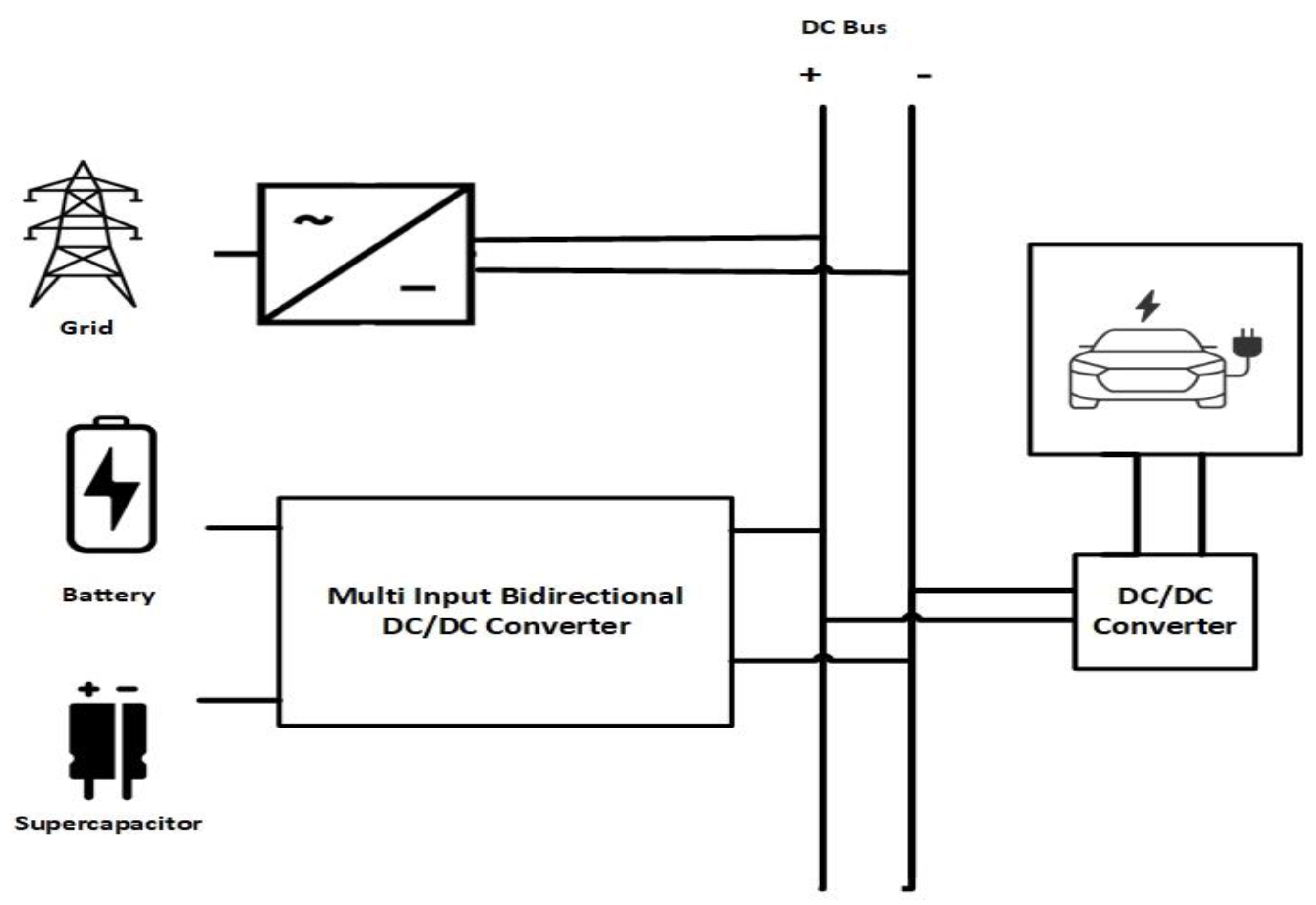
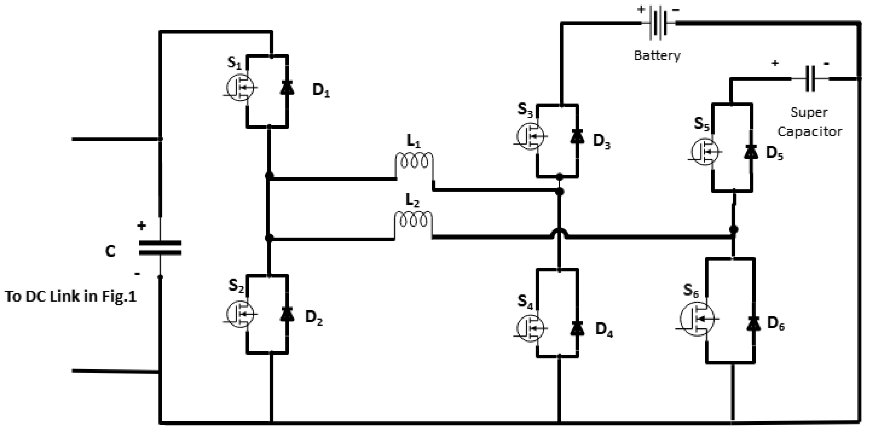
2. Proposed Topology

2.1. Design of the Multi-Input Converter

The proposed fast-charging station in Figure 1 uses a multi-input converter that can work in five operation modes to simultaneously or individually charge and discharge the energy storage devices as well as to exchange power between them. The battery and supercapacitor are used to form a hybrid energy storage system to combine the high-energy density from the battery and the high-power density from the supercapacitor. The converter consists of six MOSFETs, two inductors, and one capacitor, as shown in Figure 2. The design can be modular by adding two power switches and one inductor to combine the switching leg. Table 2 shows the equations used to calculate the minimum values of inductors L 1   and L 2   , where D is the duty cycle, Ts is the total period, d1 is the ratio of the on-time of switch S3 to total switching period Ts and, similarly, d2 corresponds to switch S2, VBt is the battery voltage, VSC is the supercapacitor voltage, and VDC is the DC link voltage, and Table 3 shows the design specifications of the proposed converter with rated values.
To avoid the worst-case scenario, protection elements will be added to the station, such as circuit breakers and fuses, to increase the safety of the station and the converter.

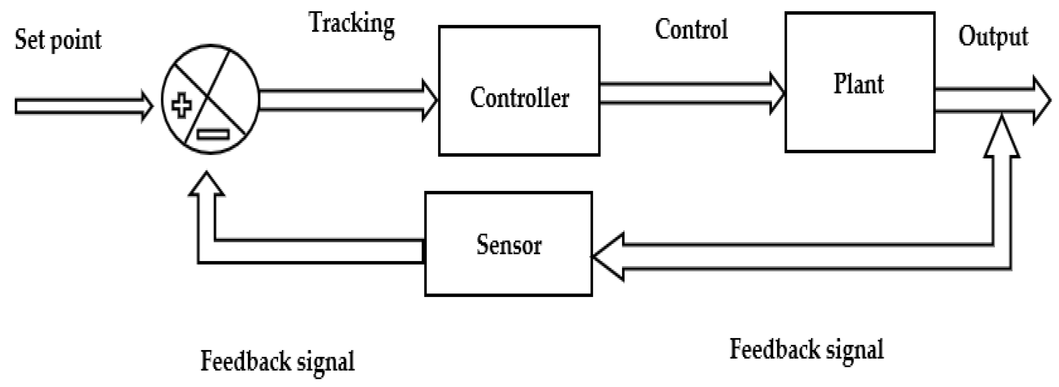
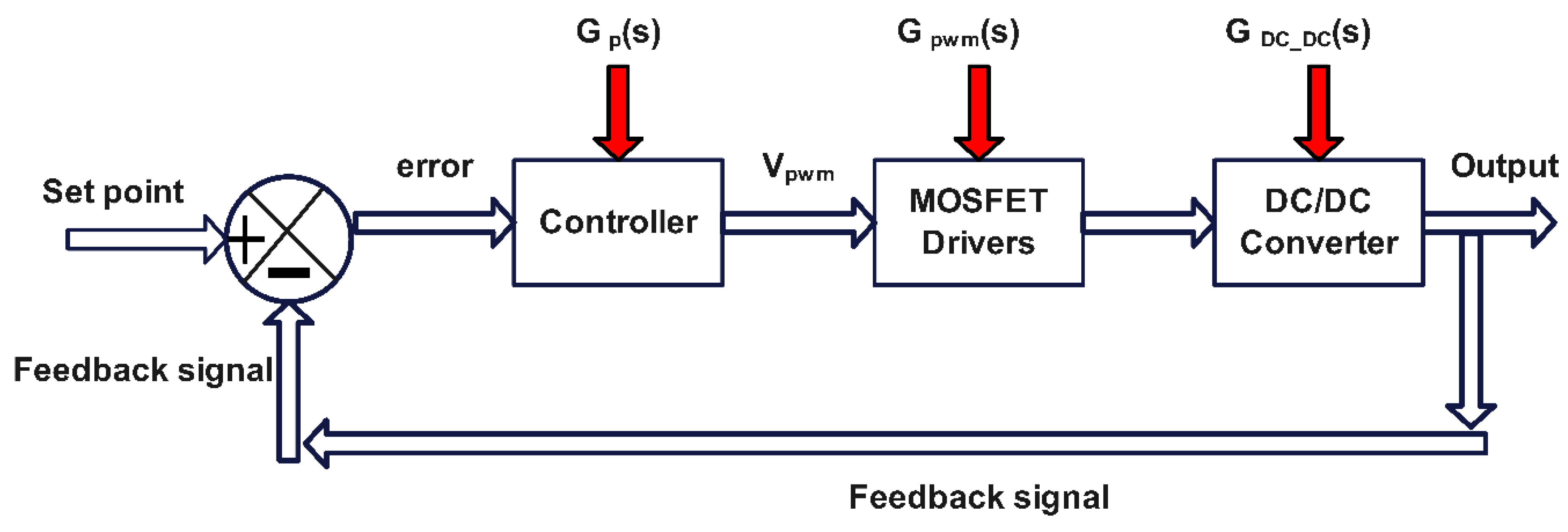
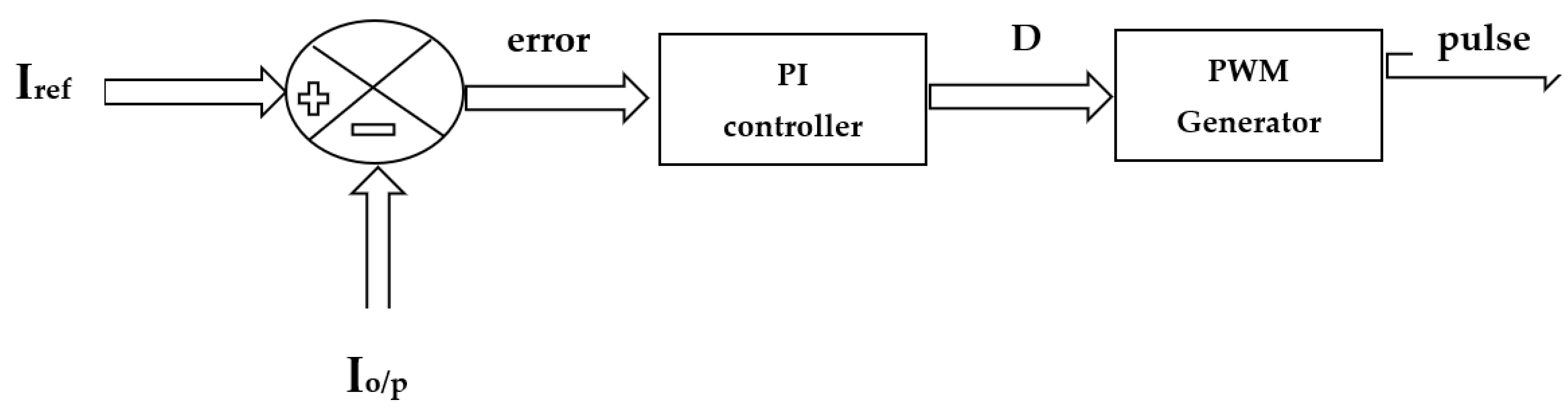
2.2. Control of the Converter

A PI controller is one of the most common control algorithms used in power electronics, especially in DC/DC converters. It has many advantages such as simplicity, reliability, and ease of implementation in linear systems. It is part of the PID controller family with three integrated constants, as shown in Figure 3, which have a control loop mechanism, employing feedback that is frequently utilized in power electronics circuits. Typically, the proportional and the integral (PI) constants are only used in DC/DC converters to control the steady-state and transient errors and to enhance the response time of the system.
The system performance and response can be optimized by tuning the constants Kp, Ki, and Kd. However, as the constants Kp and Ki are typically only used in DC/DC converters, the output currents and voltages can be adjusted by tuning them and acquiring the desired process requirements. The error value is the difference between the feedback signal and the desired setpoint. The controller attempts to reduce it by modifying a controlled variable (e), the tracking error, as shown in Figure 4.
The error signal will be delivered to the PID controller, and the signal immediately after the controller will match the proportional gain times the error magnitude plus the integral gain times the integral of the error plus the derivative gain times the derivative of the error, where this signal will be sent to the plant to obtain the desired output.
The PI controller is used for the voltage control for the buck and boost stages of the multi-input DC/DC converter. The closed-loop transfer function of the PI controller’s first-order system is:
  G ( s ) = ( K p + K i s ) · k τ · s + 1 + ( K p + K i s ) · k
where τ is the time constant and K is the DC Gain. Equations (2)–(4) were used to implement the controller algorithm in Figure 5.
V o u t ( s ) V s e t   p o i n t ( s ) = G ( s ) 1 + G ( s )
G ( s ) = G p ( s ) · G P W M ( s ) · G D C _ D C ( s )
G c o n v e r t e r ( s ) = G P W M ( s ) · G D C _ D C ( s )
As shown in Figure 5, the output signals of the PI controller determine the suitable duty ratio for switching the MOSFETs gates to obtain the desired operation mode. The same algorithm is used in the downscale DC/DC converter to control the charging current of the EV. The system is underdamped by regulating the value of the proportional coefficient K p = 3 and the integral coefficient K I = 5 to minimize the steady-state error. To make the whole system stable, the lead–lag compensator was designed using Equation (5), with Kp = 3 and Ti = 7.5758 × 10⁻⁴.
C i L = K p ( 1 + 1 T i S )

2.3. The Operation Modes of the Converter

The proposed converter works in five different operation modes, as we will discuss later, to transfer the power between the DC link and energy storage devices simultaneously or individually and to exchange power between them. The five operating modes of the converter are:

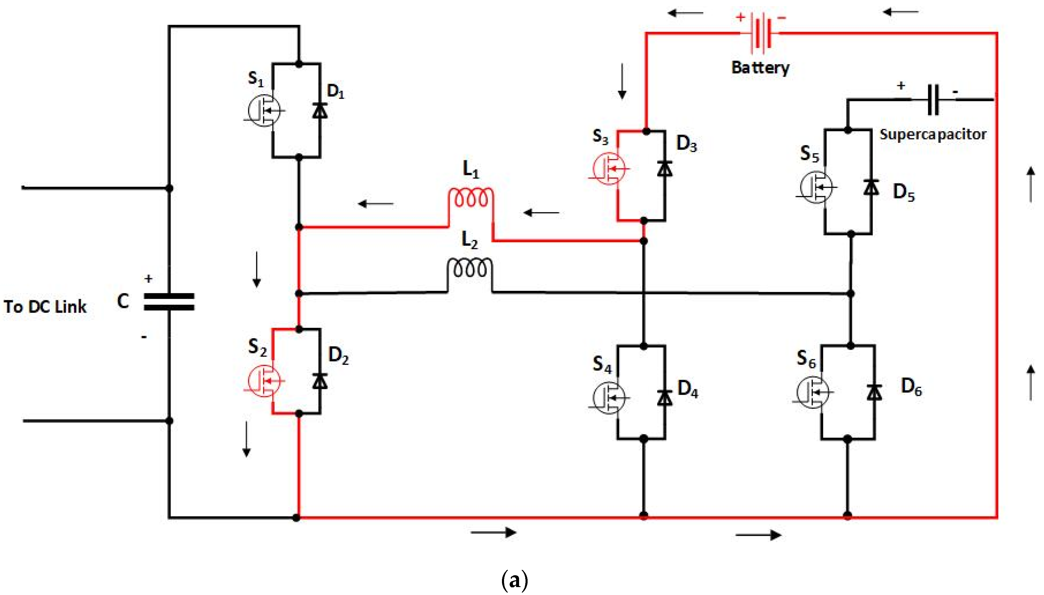
2.3.1. Mode 1: Battery to DC Link

The inductor L 1 is charged and discharged during this operation mode in three-time intervals, T 1 , T 2 , and T 3 , to discharge the battery only in the DC link to charge the electric vehicle’s (EV’s) battery. The switches S 2   and S 3 are turned on in the first-time interval to charge the L 1 , as shown in Figure 6a. In the second interval, the L 1 discharges through diodes D 1 and D 4 while switches S 2 and S 3 are turned off to supply the DC link in Figure 6b. To maintain the continuous discharging of energy from L 1 in the DC link, the switches S 1 and S 4 are turned on during the third time interval, as opposed to the diodes in T 2 . The switches S 1 and S 4 operate as synchronous rectifiers to reduce the voltage drop to a level of about 0.2 V; hence, the system efficiency is improved, as shown in Figure 6c. Under the steady-state condition, the relation between DC link voltage as an output and battery voltage as input is expressed using Equation (6):
V D C = T 1 T 2   + T 3   ·   V B T = D 1 D   ·   V B T
where D is the duty cycle ratio defined by T 1 T S , and T S is the total period of the switching cycle. The battery voltage is boosted to the DC link when working in a duty cycle equal to D > 0.5.
The DC link charges the battery by reversing the current in L 1 . Under the steady-state condition, and taking into consideration D to be T1/TS, the relation between the DC link voltage and battery voltage can be expressed using Equation (7).
V B T = T 1 T 2   + T 3   .   V D C = D 1 D   .   V D C

2.3.2. Mode 2: Supercapacitor to DC Link

This operating mode is used to utilize the merit of the high-power density of the supercapacitor to charge the EV in less time. The inductor L 2 is charged and discharged in the DC link in three-time intervals, T 1 , T 2 , and T 3 , similar to the previous operation mode. The switches S 2 and S 5 are turned on in the first-time interval to charge the L 2 . In the second interval, the L 2 discharges through diodes D 1 and D 6 while switches S 2 and S 5 are turned off to supply the DC link. In the third interval, the switches S 6 , S 1 are turned on for the continued discharging of L 2 in the DC link and to reduce the voltage drop of the diodes. Equation (8) shows the voltage of the DC link V D C   as an output voltage as a function of the supercapacitor V S C input voltage.
V D C = T 1 T 2   + T 3   ·   V S C = D 1 D   ·   V S C
where D is the duty cycle ratio equal T 1 T S . To charge the supercapacitor from the DC link, the current flow reverses in L 2 and operates at D < 0.5. Equation (9) expresses the relation between the input and output voltage considering the duty ratio D to be T1/TS.
V S C = T 1 T 2 + T 3   ·   V D C = D 1 D   ·   V D C

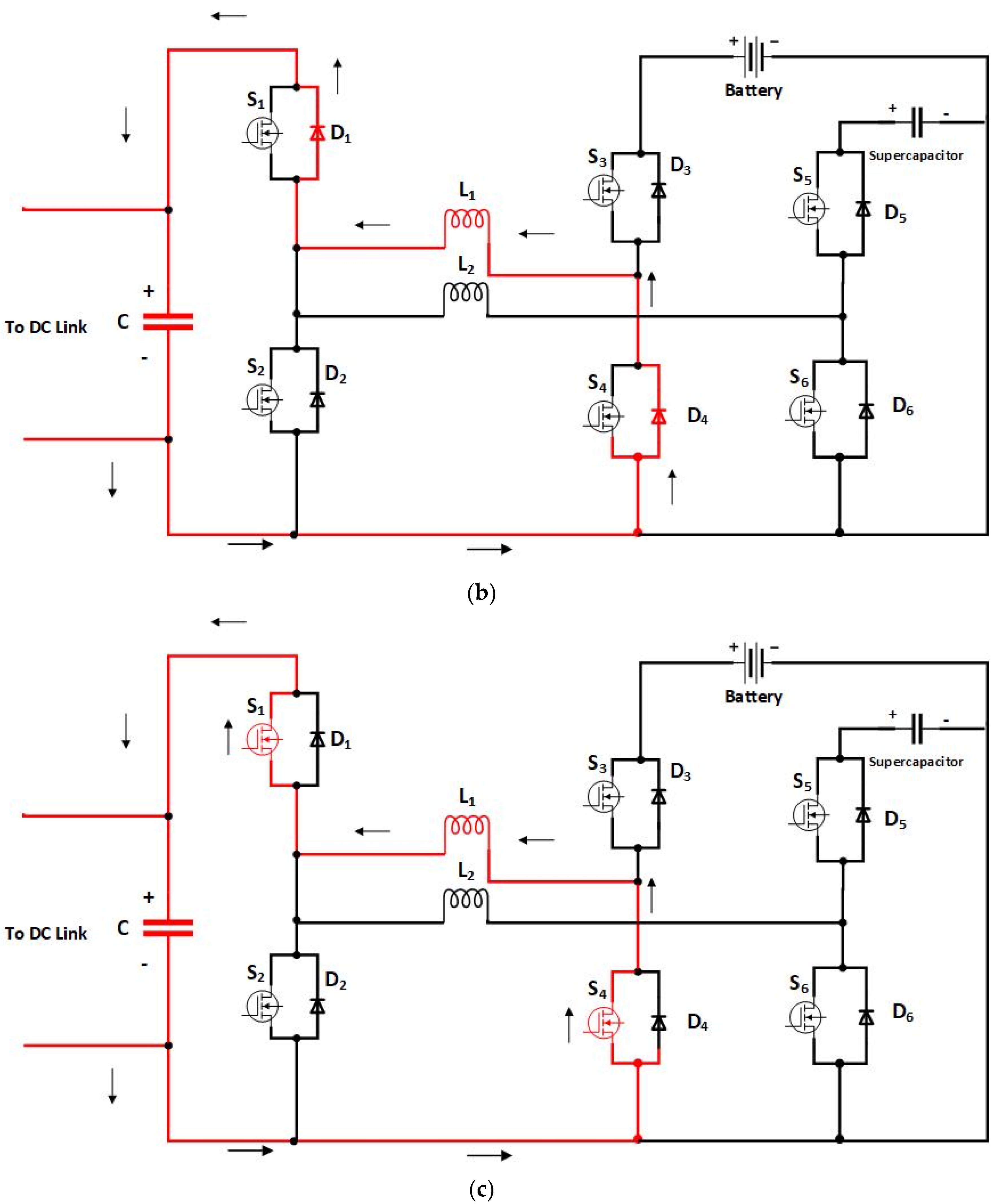
2.3.3. Mode 3: Battery and Supercapacitor

In mode 3(a), the supercapacitor can be charged from the battery. The converter boosts the battery voltage V B T to charge the supercapacitor, as shown in Equation (10), using the switches S 3 ,   S 5 , and S 6 .
V S C = T s T 2   + T 3   ·   V B T = 1 1 D   ·   V B T
The lifetime of the battery can be increased by charging it from the supercapacitor using mode 3(b). The switches S 3 ,   S 5 , and S 6 are turned on to reverse the current through the inductors, as the battery can be charged in the buck operation mode using Equation (11).
V B T = T 1 T s   ·   V S C = D   ·   V S C
The switching sequence of the power switches in the three-time intervals of the previous operation modes is summarized in Table 4.

2.3.4. Mode 4: Battery and Supercapacitor to DC Link

In this operation mode, the load from the grid can be mitigated during the peak hours by charging the EV from the battery and the supercapacitor simultaneously, as the EVs consume high power and increase the load on the grid. As well, this mode can be utilized to reduce the charging cost by charging the battery and the supercapacitor during the off-peak hours and discharging them during the peak hours. Inductors L 1 and L 2 are charged and discharged in five-time intervals, represented in Table 5, to supply the DC link simultaneously from the battery and the supercapacitor using Equations (12) and (13).
V B T = T 4 + T 5 T 1   .   V D C = T s d 2 T s d 1 T s   .   V D C = 1 d 2 d 1   .   V D C
V S C = T 4 + T 5 T 1 + T 2 +   T 3   .   V D C = T s d 2 T s d 2 T s   .   V D C   = 1 d 2 d 2   .   V D C
where d 1 is the ratio of the on time of switch S3 to the total switching period TS and, similarly, d2 corresponds to switch S2.

2.3.5. Mode 5: DC Link to Battery and Supercapacitor

In contrast to operation mode 4, during the off-peak hours, the DC link can charge the energy storage devices simultaneously to save the cost of energy. By using Equations (14) and (15), and in the same way as in mode 4, inductors L 1 and L 2 will be charged and discharged in five-time intervals to charge the supercapacitor and battery.
V B T = T 1 + T 5 T 1 + T 2 + T 3 + T 5   ·   V D C = T 1 + T 5 T s T 4   ·   V D C = d 1 d 2   · V D C
    V S C = T 1 + T 5 T s   ·   V D C = d 1   ·   V D C

3. Losses and Efficiency of the Proposed Converter

The switching losses and conduction losses (as shown in Table 6 and Table 7) are the main losses of the proposed converter. As the MOSFETs of the converter are exposed to high voltage and current during a transition between the on and off states, this creates switching losses in the converter. By using Equation (16), the switching losses in the different operation modes can be calculated.
P S = V D I D     d t
where V D   and I D   are the voltage and current of the MOSFET. The resistive elements of the MOSFETs dissipate power and create conduction losses as current is conducted through the device. The resistive parameter is described as on-resistance, or RDS(ON), and it equals 0.1 Ω in the proposed converter. The conduction losses can be calculated using Equation (17).
P c = I 2 · R DS(ON)
Therefore, the total losses will be:
  P T = P s + P c
The switching and conduction losses in the different operation modes are summarized in Table 5, Table 6 and Table 7 based on Equations (17) and (18).
The efficiency of the proposed converter in the different operation modes is summarized in Table 8 based on Equation (19).
efficiency = P o p P i n

4. The Proposed Fast-Charging Station

As mentioned before, the proposed converter is used to charge EVs individually or simultaneously from energy storage devices. The energy storage devices are connected with the grid utility to the DC link, as shown in Figure 1. This DC link is connected to a step-down converter to reduce the DC link voltage and increase the charging current of the EV as well as control the charging rate.

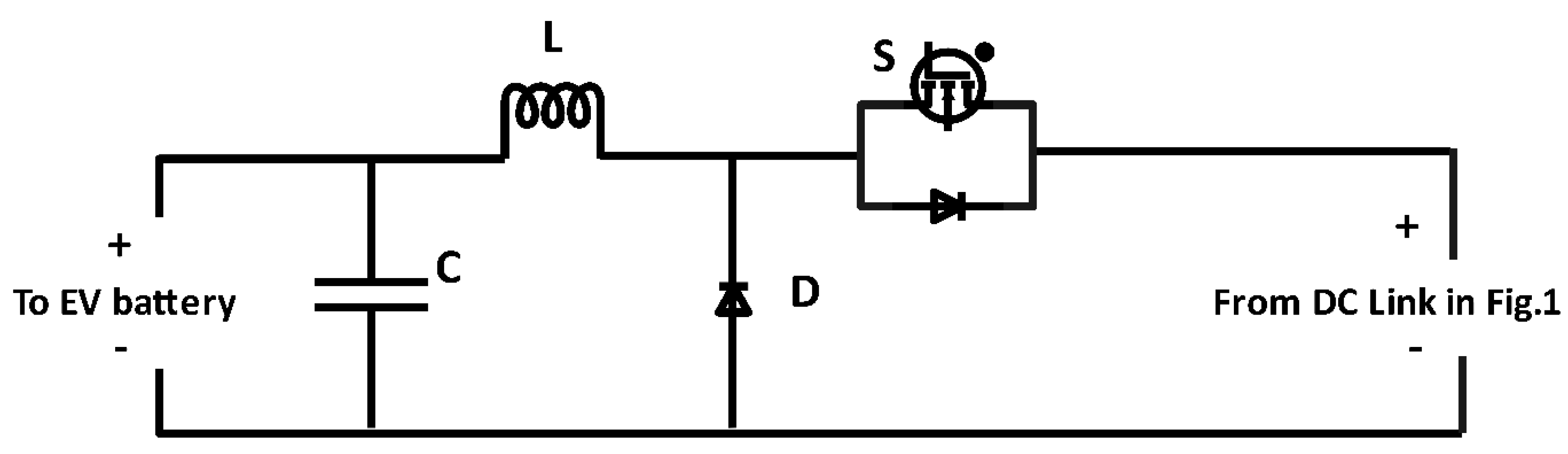
4.1. The Design of the Buck Converter

The step-down DC/DC converter shown in Figure 7 consists of MOSFET switch S to charge and discharge the inductor L and diode D to prevent the current from passing through it during the on-state of the switch as its reversed biased by voltage. The capacitor C is used as a filter for voltage ripples. During the on-state, the switch S is turned on, the current through inductor L is increased, and the voltage across the inductor will be
V L   = V i n V O
as in this case, the V i n will be the DC link voltage, and the V O will be the output voltage to charge the EV’s battery. In the off-state, the switch S is turned off, the diode D will be forward biased, and the voltage across the inductor will be
  V L   = V O
and the current through the inductor will decrease and flow through the freewheeling diode D and the capacitor C.
The inductor is selected to make the converter work in the continuous operation mode and reduce the current ripples and is calculated using Equation (22)
L = ( 1 D ) R 2 f
where R is the resistive load and D is the duty cycle. Similarly, the capacitor is selected and calculated using Equation (23) to reduce the output voltage ripples and handle the required ripple current stress.
V C = V S   D ( 1 D ) R 8 L C f 2
The buck converter works at a switching frequency f 20 kHz to reduce the size of the inductor and the capacitor. Table 9 shows the design specification of the proposed buck converter [15].

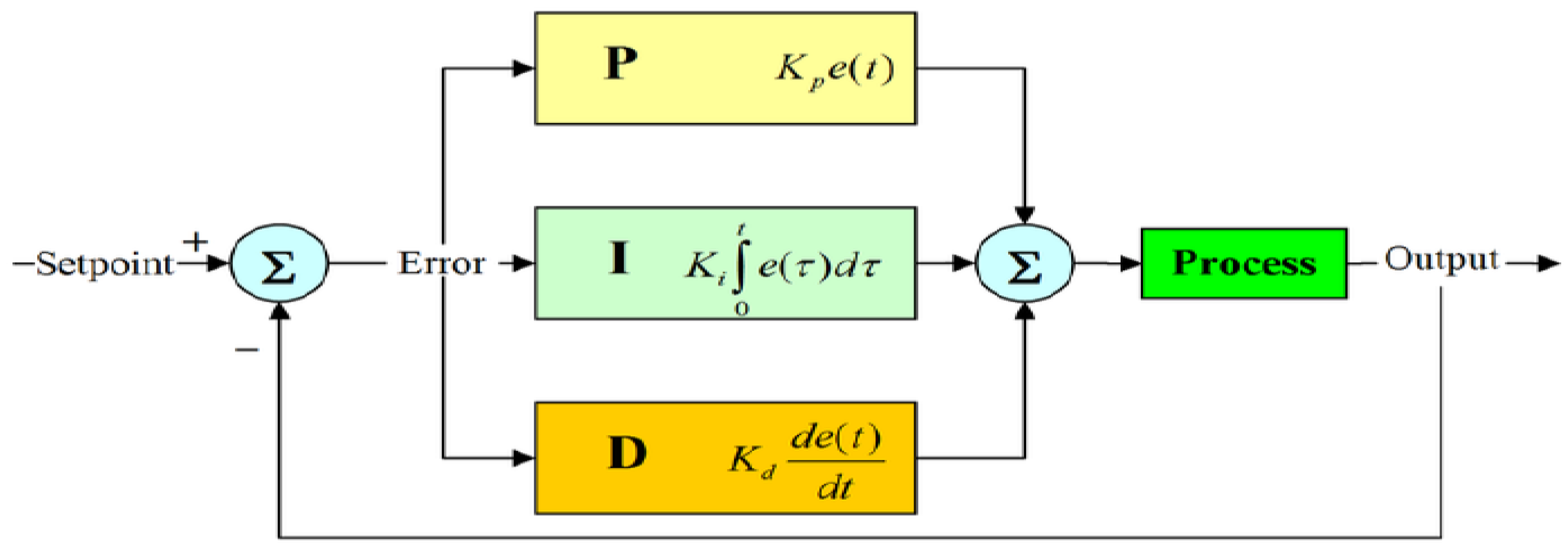
4.2. The Control of the Buck Converter
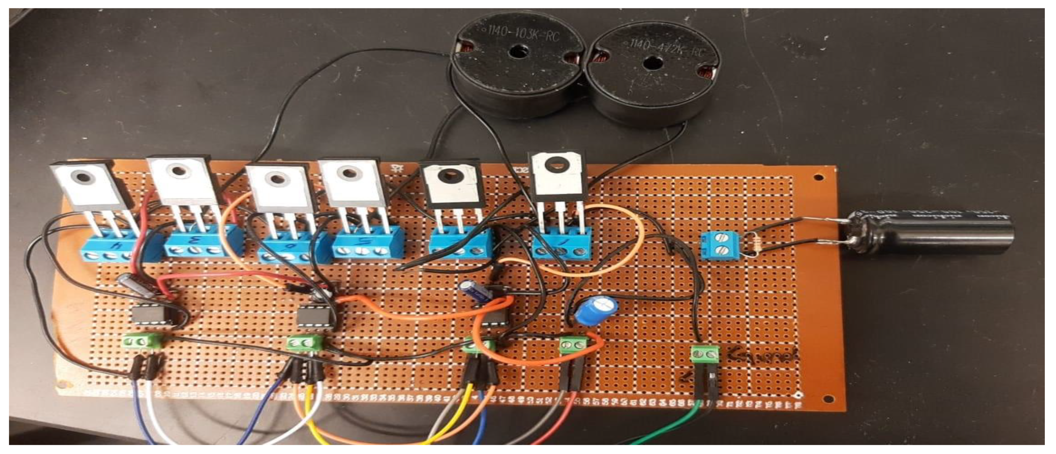
The multi-input converter was based on voltage control to sustain the DC link voltage at 500 V. In contrast, the buck converter is based on current control, as shown in Figure 8, to control the charging current of the EV. The proportional integral (PI) controller was chosen to also to control the charging current. The PI controller minimizes the error between the output current and the reference charging current to determine the desired duty ratio for generating the pulses of the switch. The system is underdamped by regulating the value of the integral coefficient KI = 5 and proportional coefficient Kp = 3 to minimize the overshoot and the steady-state error. These values were obtained using the same Equations (1)–(5).

5. Results

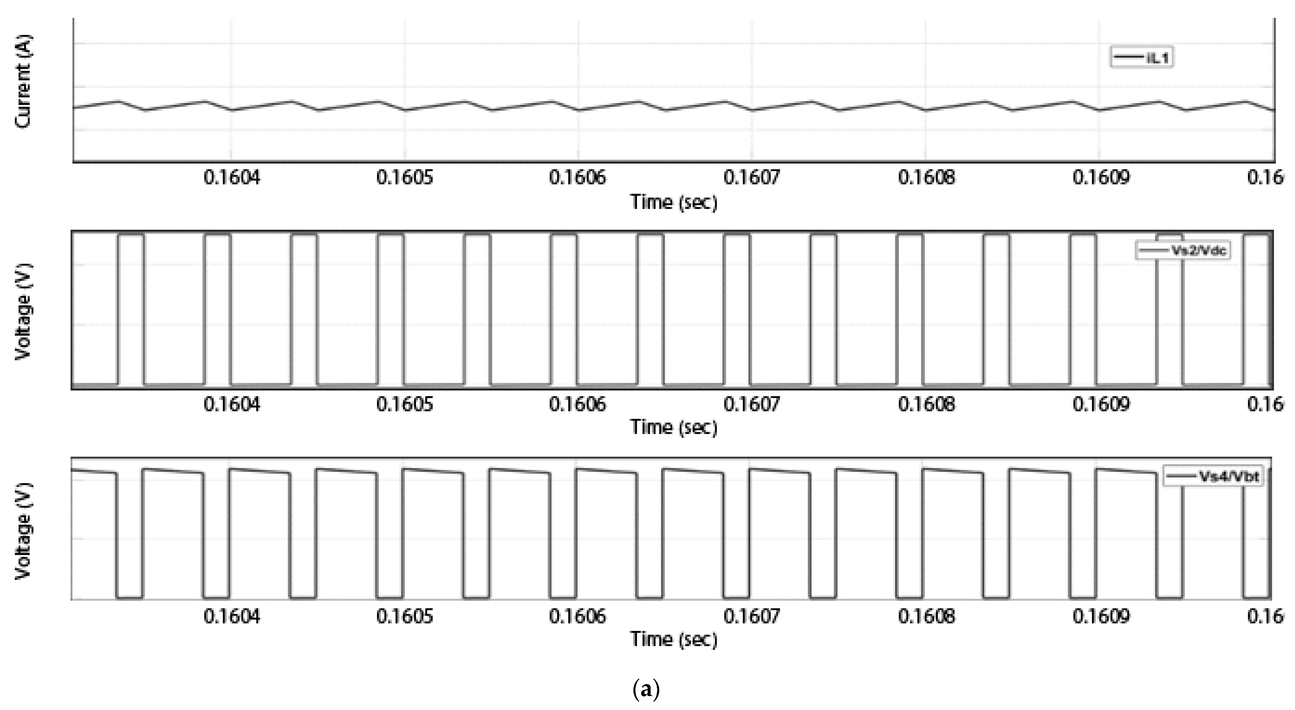
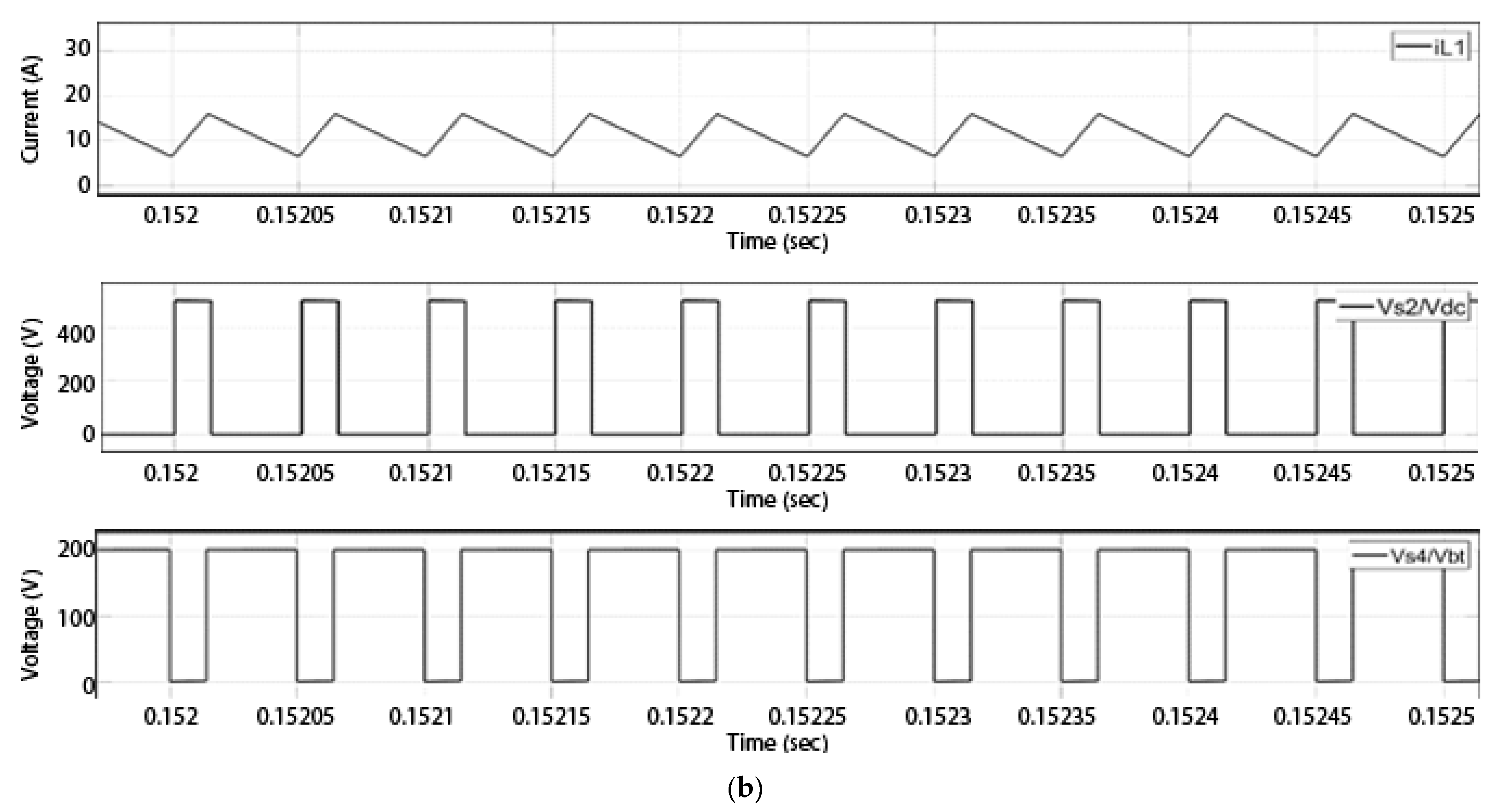
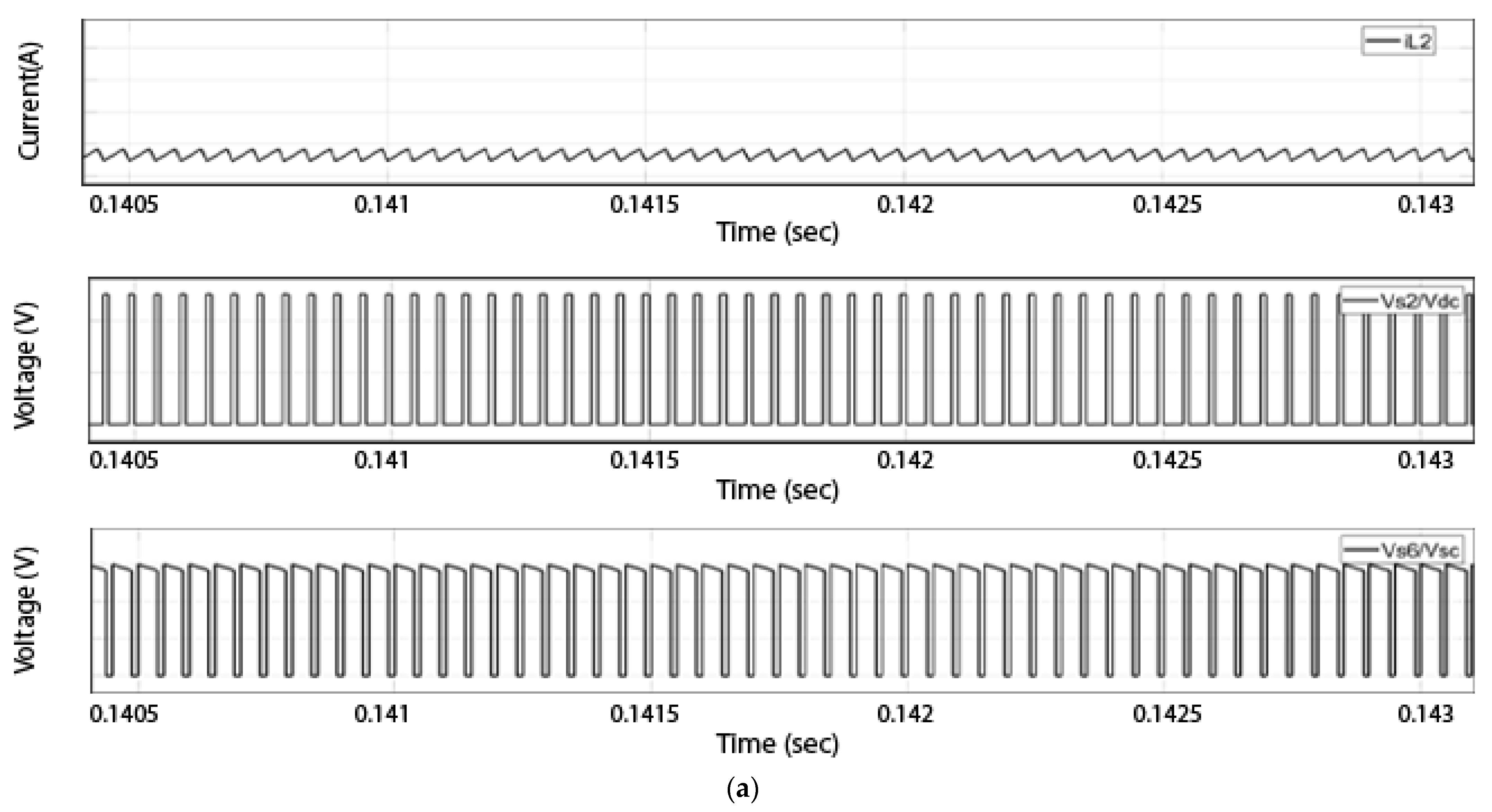
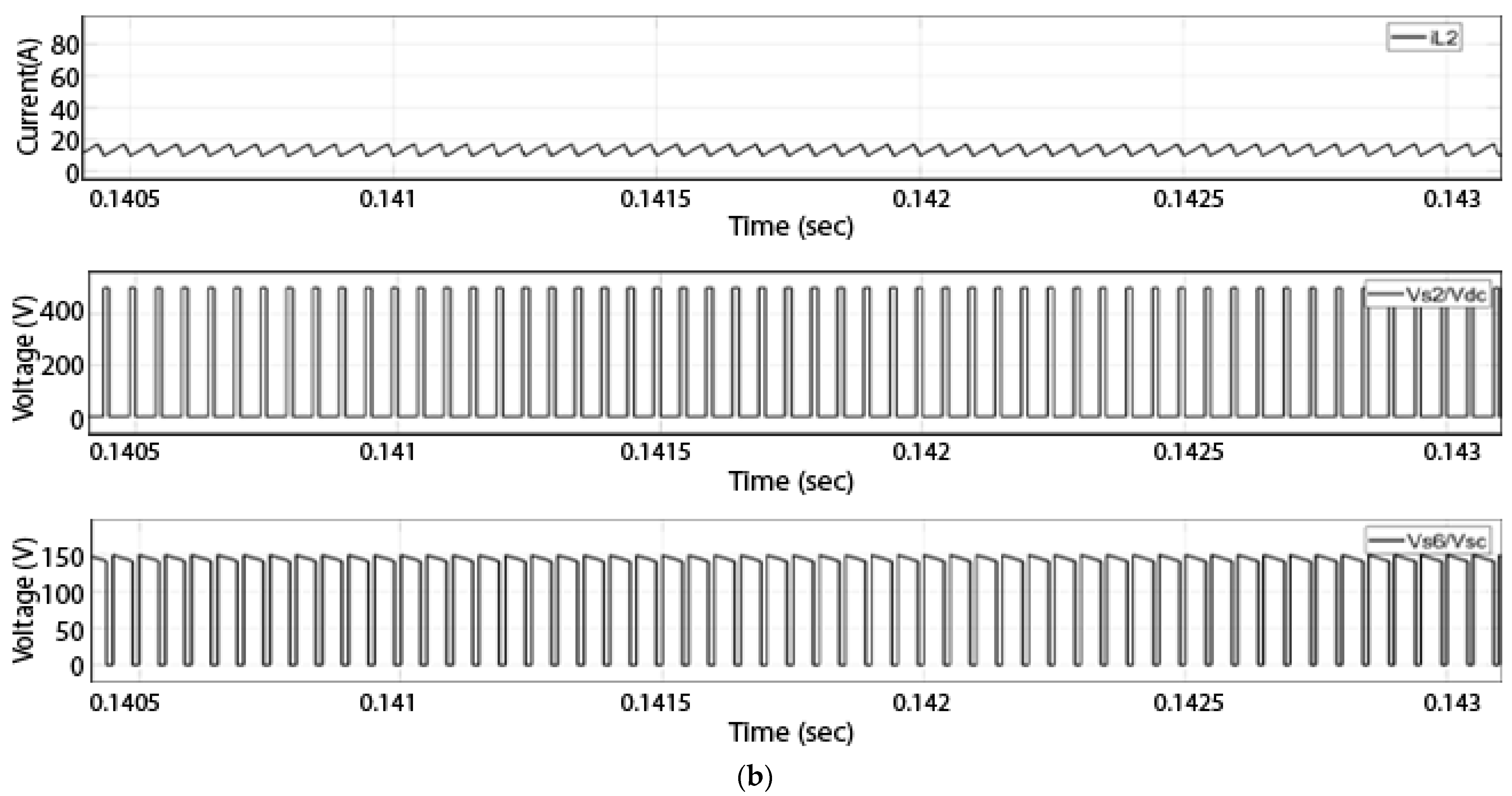
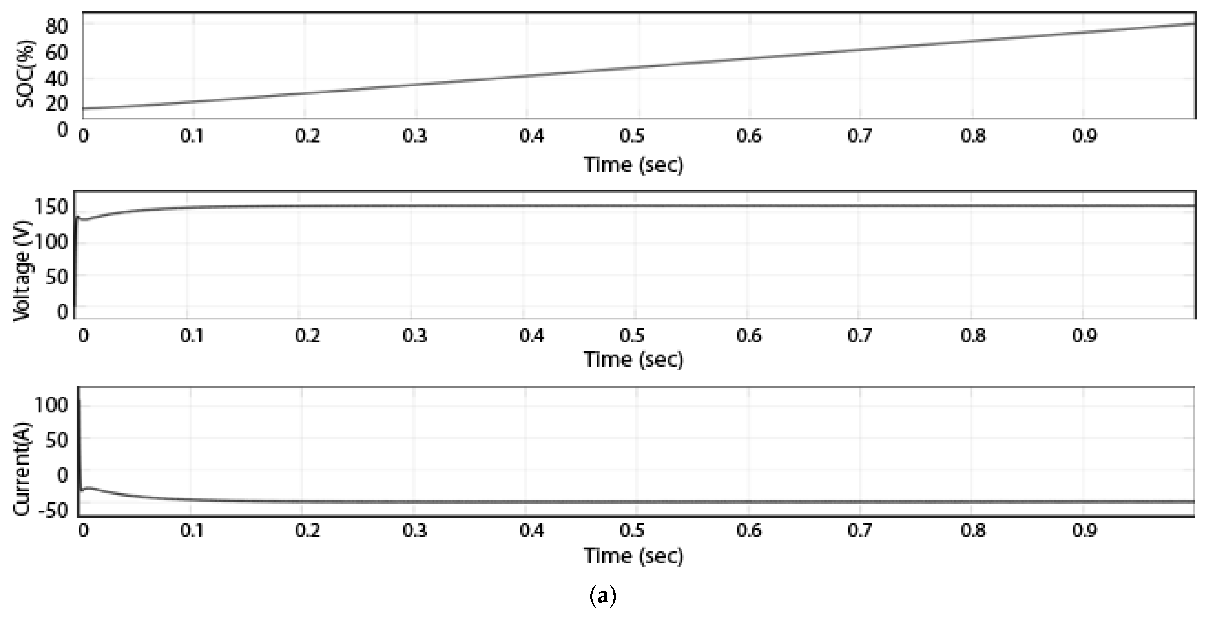
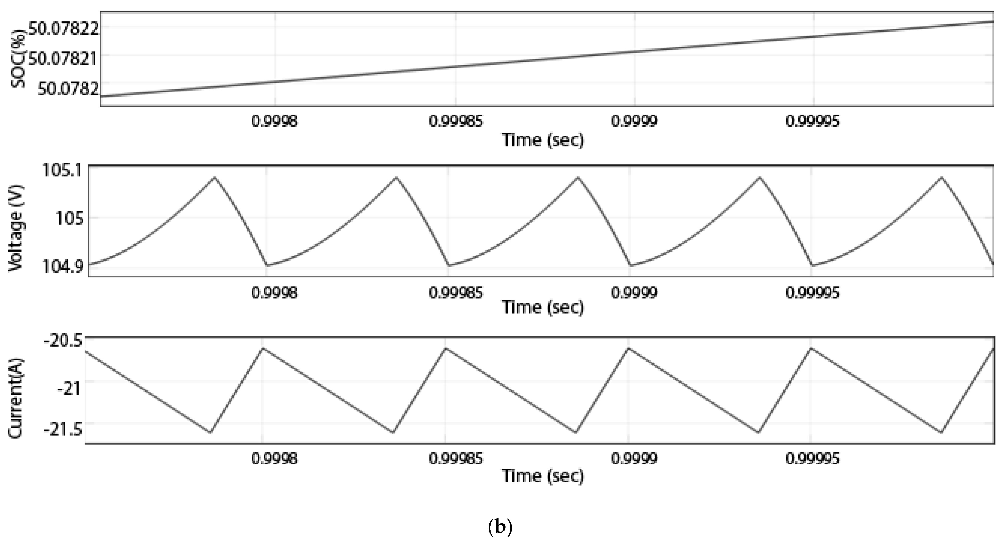
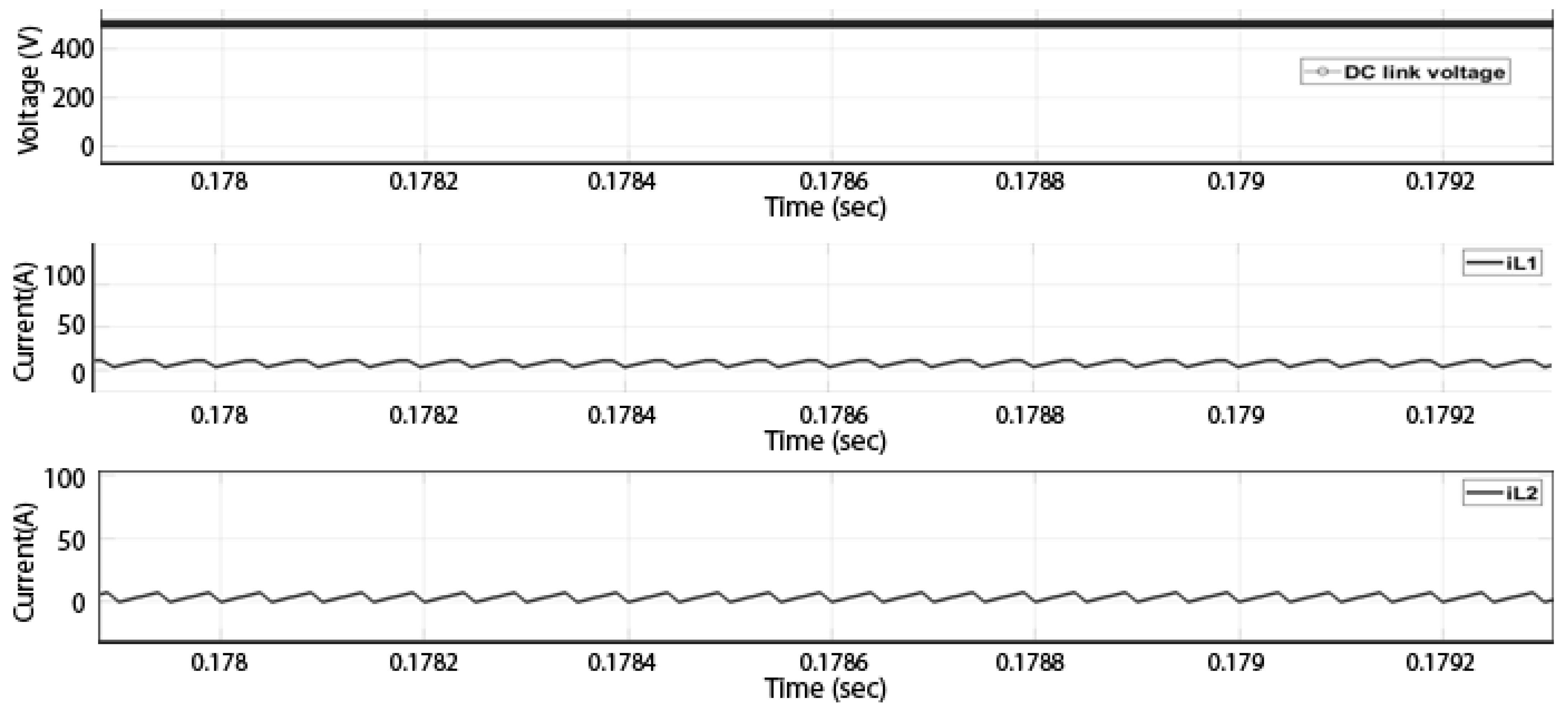
5.1. Simulation Results

MATLAB/Simulink was used to obtain the different results of the proposed converter and verify its analysis in the different operation modes. Figure 9a shows the battery was boosted from 200 V to 500 V to discharge in the DC link through L 1 in mode 1(a). Based on the switching sequence in this mode, the switch S 2 works complementarily with switch S 4 , as the voltage across S 2 presents the DC link voltage, and the voltage across S 4 presents the battery’s voltage. In mode 1(b), the battery is charged from the DC link by reversing the current in the inductor L 1 in the average current of 15 A, as shown in Figure 9b, and similarly, the voltage across S 2 presents the DC link’s voltage, and the voltage across S 4 presents the battery’s voltage. In mode 2(a), the energy transferred from the supercapacitor to the DC link as voltages across switches S2 and S6 show the DC link and supercapacitor voltage, respectively, along with their states. As shown in Figure 10a, the supercapacitor’s voltage is boosted from 160 V to the DC link’s voltage of 500 V by charging the inductor L 2 . By using the same switches and by reversing the current in the inductor L 2 , the supercapacitor charges from the DC link by reducing the voltage from 500 V to 160 V, as shown in Figure 10b. Power can be exchanged between the battery and supercapacitor, as shown in Figure 11a,b, in mode 3(a) and mode 3(b), respectively, using switches S3, S5, and S6. The SOC of the supercapacitor increases with a low-voltage ripple of charging, and the charging current is negative, which means the current enters the supercapacitor, as shown in Figure 11a. Similarly, the voltage and current ripple of charging the battery from the supercapacitor was less than 0.2 V, as shown in Figure 11b. In mode four, the DC link is boosted to 500 V from the battery’s voltage of 200 V and the supercapacitor’s voltage of 160 V simultaneously with low-voltage ripples through inductors L 1 and L 2 , as shown in Figure 12. Simultaneously, the supercapacitor and the battery can be charged from the DC link to their voltages by reversing the currents through inductors L 1 and L 2 as well, as shown in Figure 13. Their SOC increases, and the charging currents are negative, which means the currents enter the energy storage devices.
To test the proposed multi-input converter charging capability to charge an EV’s battery from the energy storage devices individually or simultaneously without the grid utility, a battery was connected to the buck converter with specifications similar to the Nissan leaf battery (350 V, 60 Ah). It was shown that the battery successfully charges the EV’s battery with a charging current of more than 25 A and an output voltage of 350 V, as shown in Figure 14. Using the supercapacitor, the SOC of the EV’s battery increased with a charging current of 25 A, as shown in Figure 15. To increase the current charging rate and to reduce the charging time, the EV’s battery is charged from the battery and supercapacitor simultaneously, as shown in Figure 16. The charging current was 50 A, and the SOC for one second of charging was higher than the SOC in the same charging time by charging from the battery or supercapacitor alone.
The simulation results show that the converter can work and charge the EVs at a power rate up to 17 kW, and this is considered level 2 in the SAE J1772 standard [16].

5.2. Experimental Results

Battery, supercapacitor bank, and restive loads in different values were used in the prototype to validate the switching sequence of the converter and the topology concept. In addition, Arduino UNO was used as a controller with an IRS 2186 MOSFET gate driver to switch the MOSFETs of the multi-input converter prototype and maintain the voltage across the gate and source of the high-side MOSFETs. The prototype of the multi-input DC/DC converter in Figure 17 was tested at a low power rate (up to 100 W) to test the functionality of the converter in different operation modes in different switching sequences and to prove the concept of the topology. The prototype in Figure 17 was used to test the capability of the converter at different power rates with different loads. Table 10 shows the design specifications of the multi-input converter prototype.

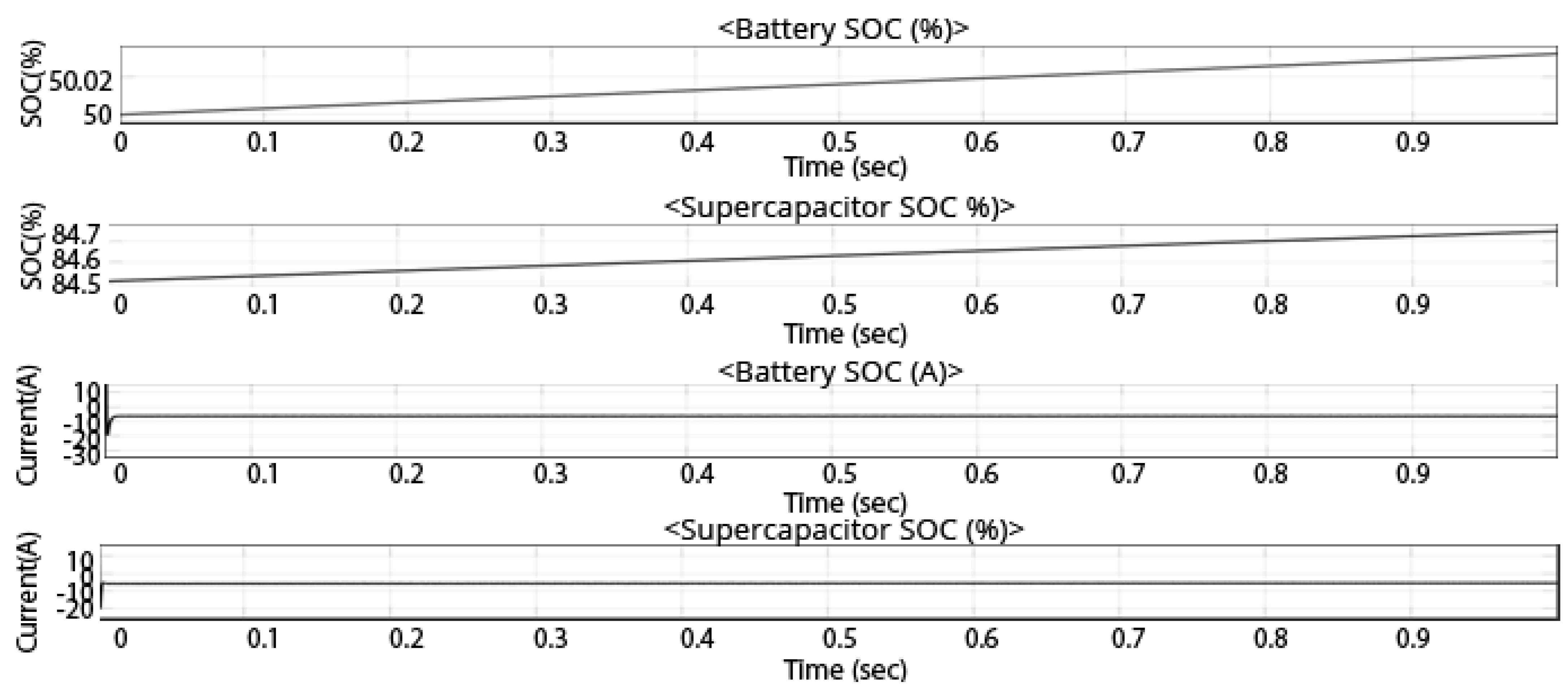
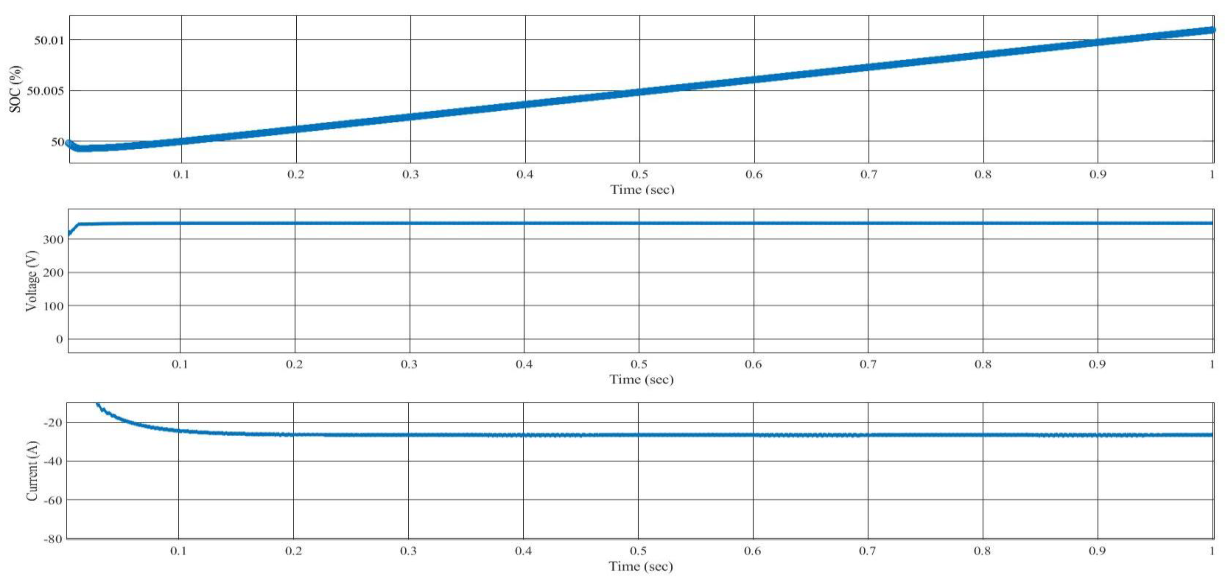
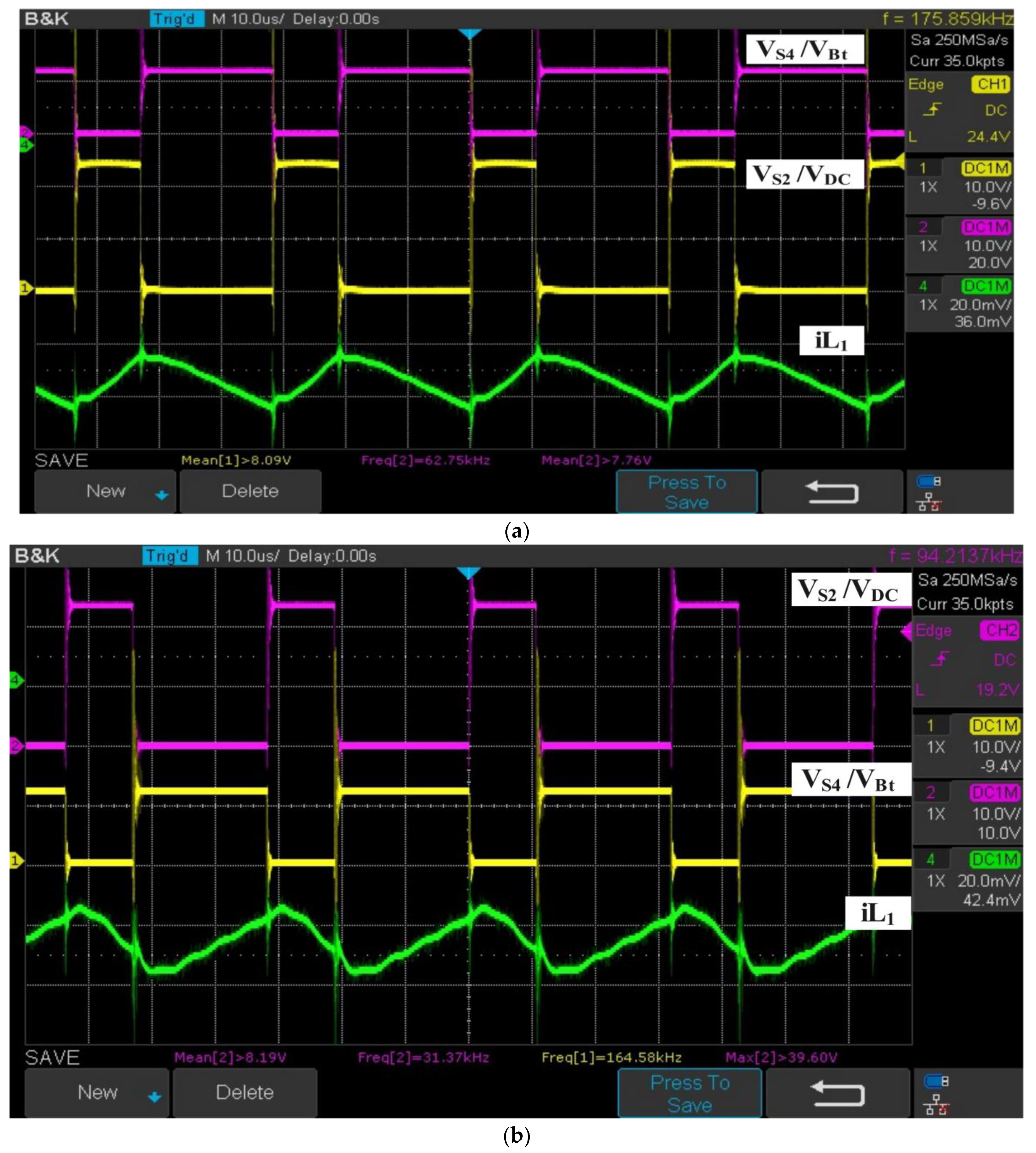
5.2.1. Supplying the DC Link from the Battery Alone

The battery’s voltage was boosted from 12 V to 24 V with complementary signals, as shown in Figure 18a, by switching the MOSFETs S3 and S2 complementarily with S1 and S4. Inductor L1 is charged when switches S3 and S2 are turned on from the battery and discharged in the DC link when the S1 and S4 are turned on, as the voltage across S 2 presents the DC link’s voltage, and the voltage across S 4 presents the battery’s voltage. Vice versa, the DC link voltage buck from approximately 24 V to 12, as shown in Figure 18b, by operating switches S1 and S4. complementary with S3 and S2. The charging current is reversed in L1 to charge the battery from the DC link, as shown in Figure 18b, which also indicates the reversal of the direction of power to approve the bidirectional power flow capability of the proposed converter.

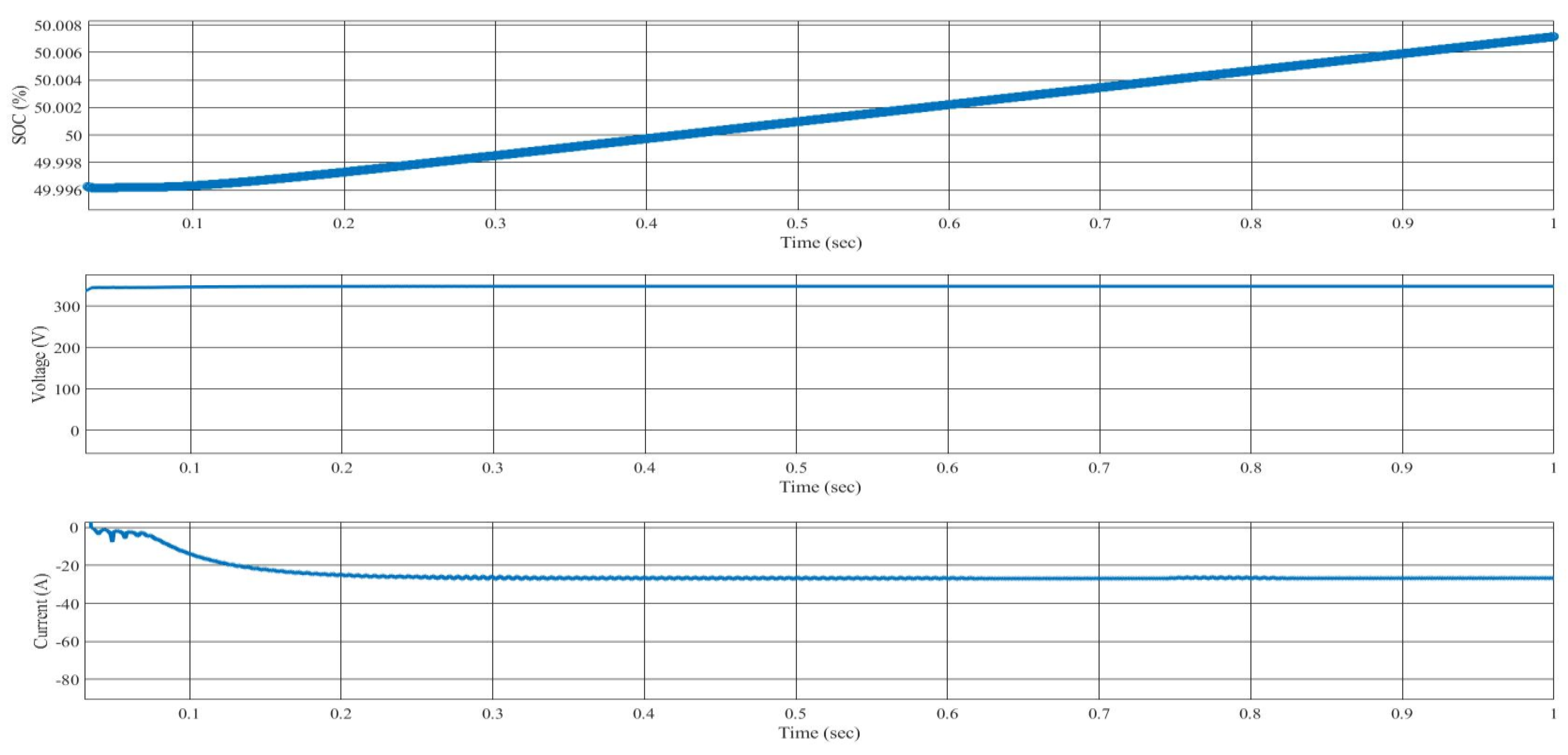
5.2.2. Supplying the DC Link from the Supercapacitor Only

Identical to the previous mode, the supercapacitor’s voltage was boosted from 15 V to 24 V with complementary signals, as shown in Figure 19a, but by switching the MOSFETs S5 and S2 complementary with S1 and S6. At this operation mode, the inductor L L2 is charged and discharged to transfer the power from the supercapacitor to the DC link. Inductor L2 is charged when the switches S5 and S2 are turned on and discharged in the DC link when the switches S1 and S6 are turned on, as shown in Figure 19a, in which the slope of the inductor current returns towards the zero value. Vice versa. the DC link voltage bucks from approximately 24 V to 15, as shown in Figure 19b, by operating switches S1 and S6 complementarily with S5 and S2. As presented in Figure 19b, the current of inductor L2 reverses its current in mode 2(b), so the iL2 slope returns to zero, which means the inductor L2 is discharging when the switches S5 and S2 are turned on.

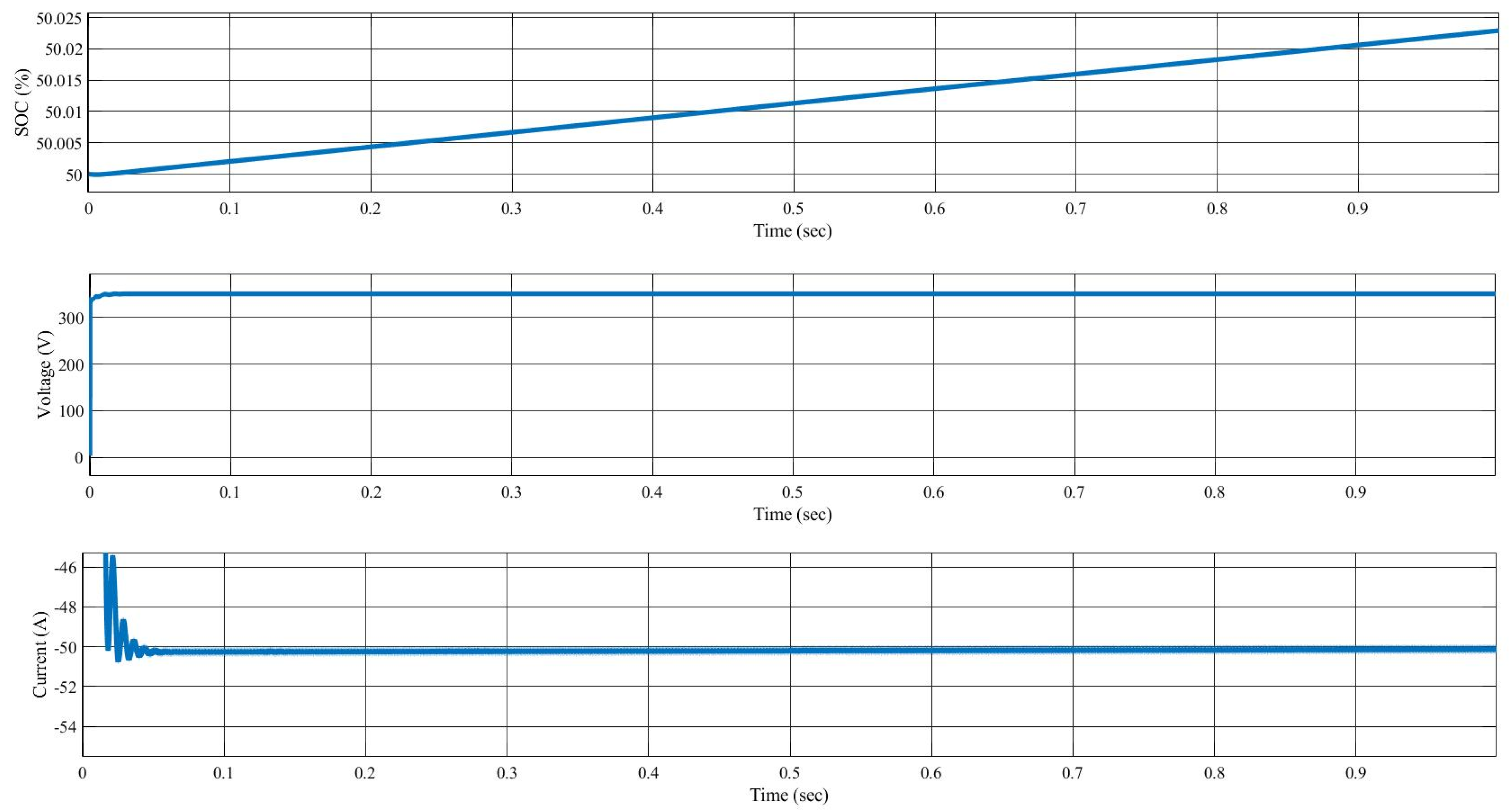
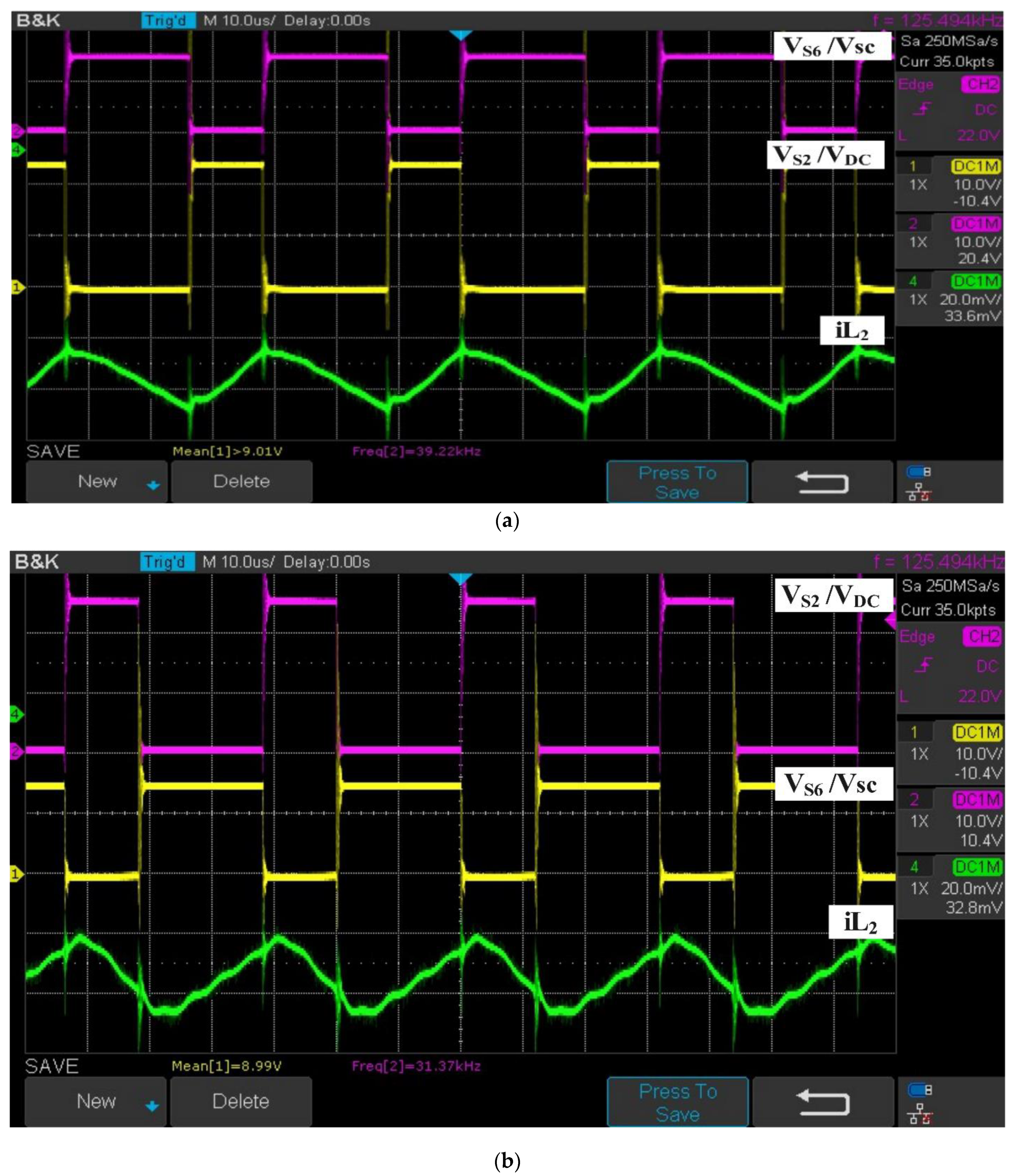
5.2.3. Supplying the Battery from the Supercapacitor

To extend the lifetime of the battery, this operation mode was used and tested as the supercapacitor voltage bucked from 15 V to 12 V using switches S3, S5, and S6. As shown in Figure 20a, the inductors L1 and L2 are charged at the same time from the supercapacitor to discharge in the battery, and vice versa, the battery voltage is boosted from approximately 12 V to 15, as shown in Figure 20b, by reversing the currents in inductors L1 and L2. Additionally, the figures below show the current ripples reduce; hence, the two inductors are series.

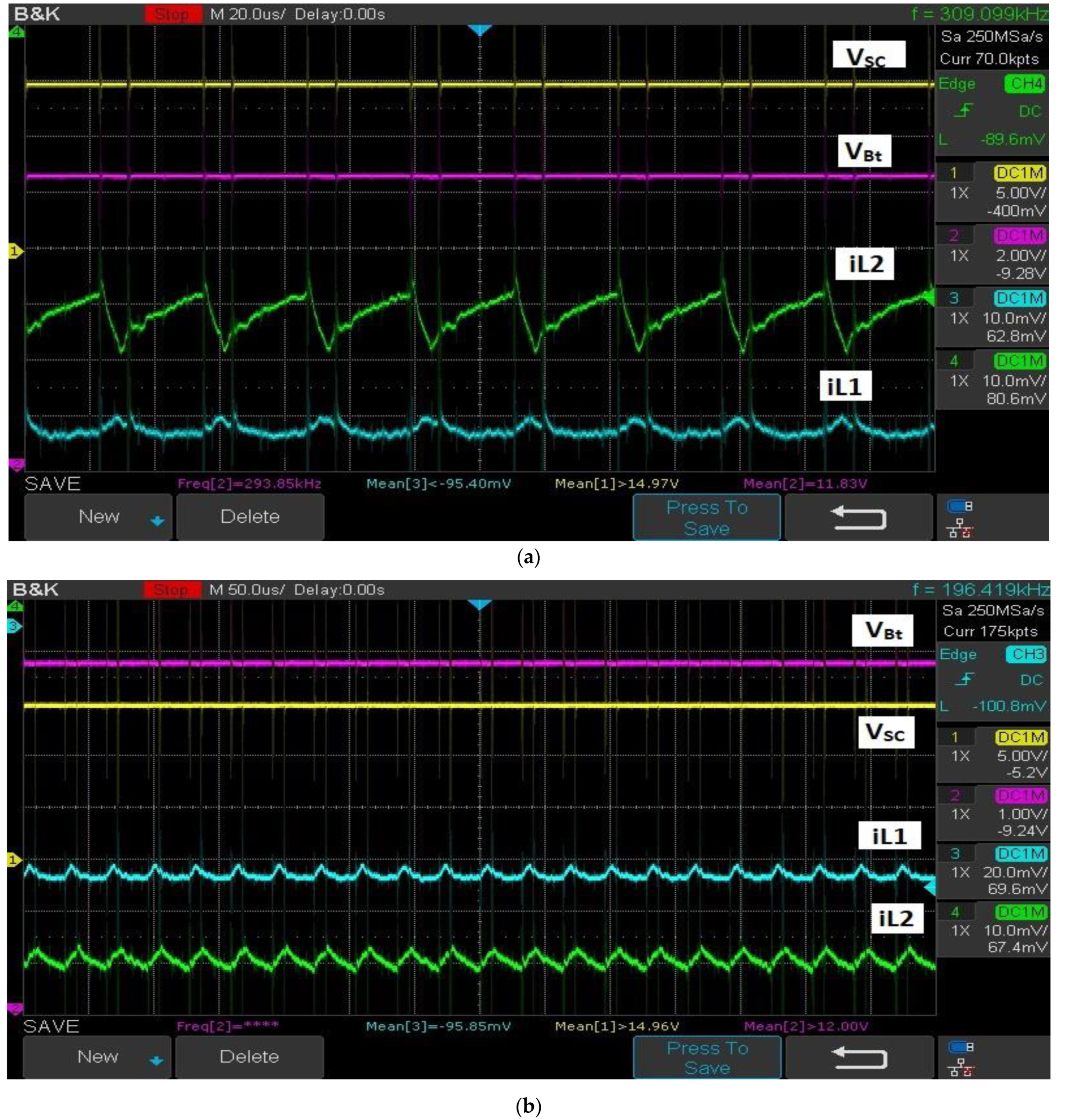
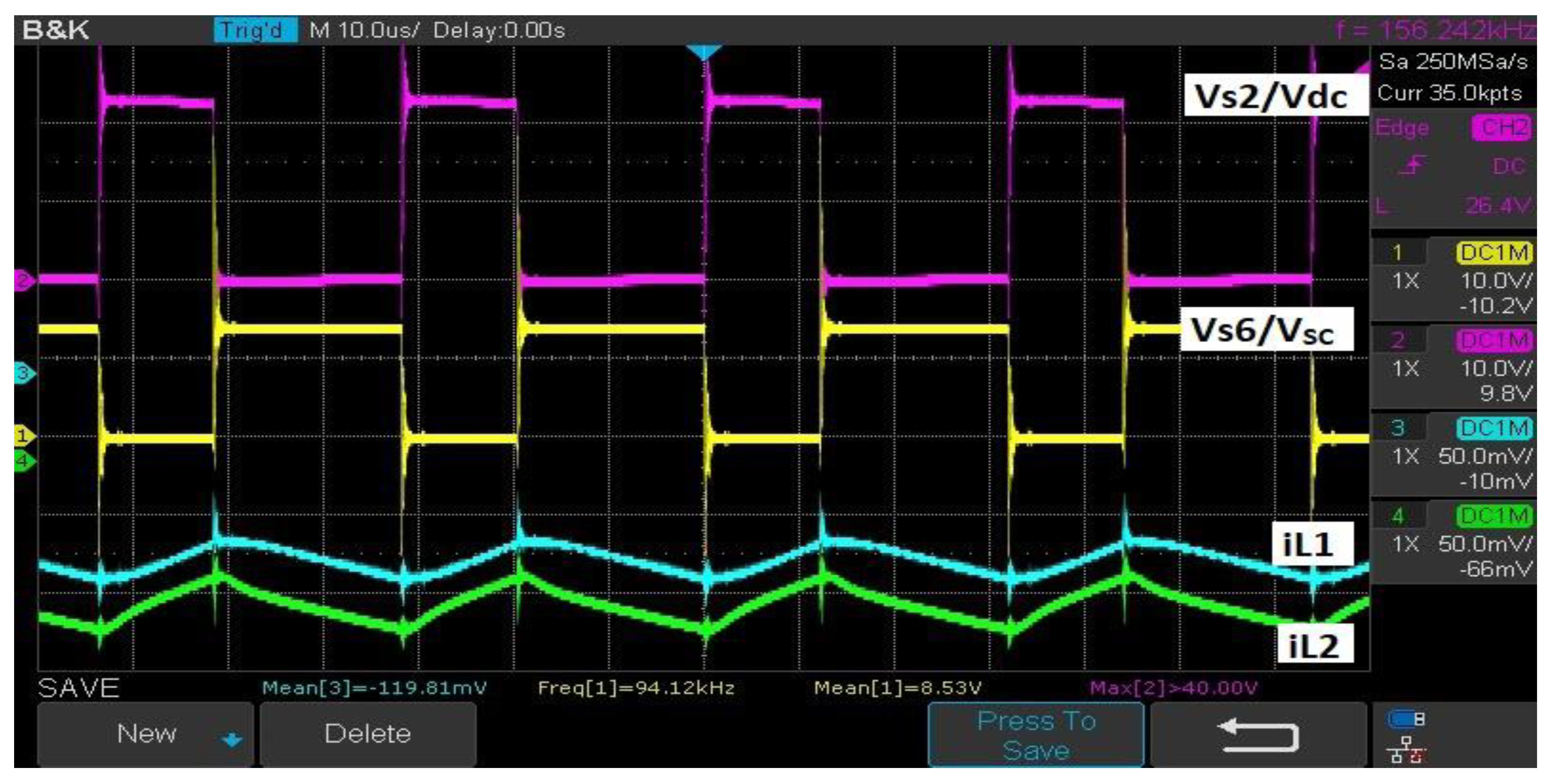
5.2.4. Supplying the DC Link from the Battery and the Supercapacitor

The inductors L1 and L2 are charged simultaneously in this operation mode from the battery, and the supercapacitor uses switches S2, S3, and S5, as shown in Figure 21. Then, the inductors discharge their energy at the DC link using switches S1, S4, and S6 to boost the DC link voltage to 24 V, as shown in Figure 21. The voltage across switch S2 represents the DC link’s voltage, and the voltage across switch S6 shows the supercapacitor’s voltage.

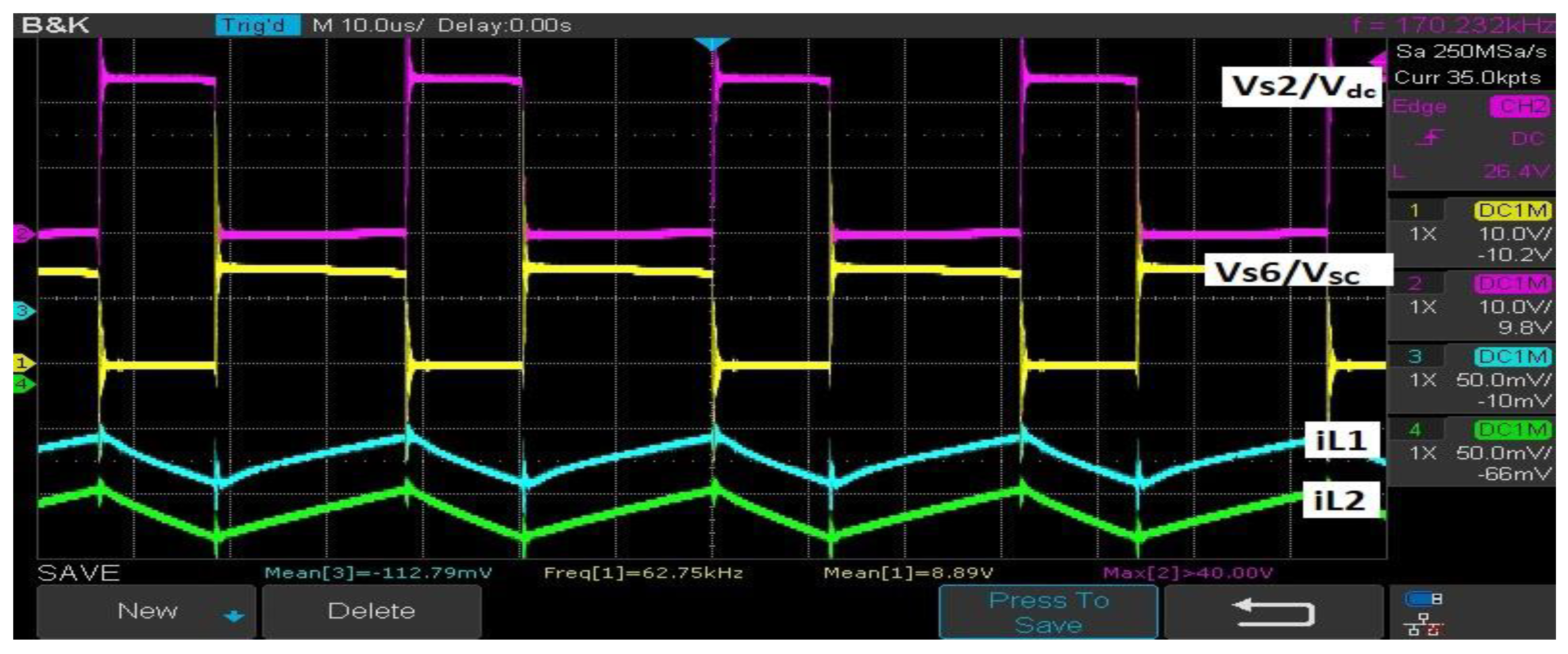
5.2.5. Charging the Battery and the Supercapacitor from the DC Link

In this operation mode, the battery and supercapacitor are charged simultaneously from the DC link by reversing the L1 and L2 inductors’ currents compared to the previous mode. Identical to the last operation mode, the inductors L1 and L2 are charged simultaneously from the DC link using switches S1, S4, and S6, as shown in Figure 22. Then, the inductors discharge their energy at the battery and the supercapacitor using S2, S3, and S5, as shown in Figure 22. The voltage across switch S2 represents the DC link’s voltage, and the voltage across switch S6 shows the supercapacitor’s voltage.

6. Conclusions

This paper discusses and analyzes a multi-input DC/DC converter to integrate a hybrid energy system for a proposed fast-charging station of electrical vehicles. The five operating modes of the converter were simulated successfully, and the losses and the efficiency of the converter were calculated in the different operation modes. The voltage ripples during most of the operation modes were less than 5%, and the efficiency was higher than 90%. The proposed converter was tested to charge a Nissan Leaf battery (350 V, 60 Ah), individually and simultaneously from the energy storage devices. The output results show the converter successfully charges the EV’s battery individually on average with 25 A, and simultaneously on average with 50 A. The experimental results validate the concept topology of the converter, specifically the switching sequence to charge and discharge the energy storage devices in different scenarios at a low power rate of (100 W). It also shows the bidirectional power flow capability of the converter. As shown in Figure 9a, they have similar waveforms to Figure 18a, but in different values, which proves the functionality of the converter, especially the switching sequence. Similarly, the output results in Figure 10b are identical to Figure 19b, which validates the simulation results and the bidirectional power flow capability. Figure 20 validates the functionality of the converter to exchange power between two energy storage devices, as presented before in the simulation results. Figure 21 and Figure 22 show the capability of the converter to charge and discharge two sources simultaneously, as shown before in the simulation results. Therefore, to operate the converter at a high-power rate, we need to adjust the values of the specification design to match the high-power rate applications. By utilizing the feature of the modularity of the converter, the input power can be enlarged by adding more power sources, hence increasing the charging power rate, and reducing the charging time. The future scope of this work is to integrate more power sources, test the prototype at a high-power rate, and optimize the control system.

Author Contributions

Conceptualization, A.E. and H.A.G.; methodology, A.E. and H.A.G.; software, A.E.; validation, A.E. and H.A.G.; formal analysis, A.E. and H.A.G.; investigation, A.E. and H.A.G.; data curation, A.E.; writing—original draft preparation, A.E. and H.A.G.; writing—review and editing, A.E. and H.A.G.; visualization, A.E.; supervision, H.A.G.; project administration, H.A.G.; funding acquisition, H.A.G. All authors have read and agreed to the published version of the manuscript.

Funding

This research is supported by NSERC 210320.

Data Availability Statement

Data is available upon request.

Conflicts of Interest

Authors have no conflict of interest.

References

  1. Khalid, M.; Ahmad, F.; Panigrahi, B.K.; Al-Fagih, L. A comprehensive review on advanced charging topologies and methodologies for electric vehicle battery. J. Energy Storage 2022, 53, 105084. [Google Scholar] [CrossRef]
  2. Khalid, M.; Ahmad, F.; Panigrahi, B.K. Design, simulation and analysis of a fast charging station for electric vehicles. Energy Storage 2021, 3, e263. [Google Scholar] [CrossRef]
  3. Kostopoulos, E.D.; Spyropoulos, G.C.; Kaldellis, J.K. Real-world study for the optimal charging of electric vehicles. Energy Rep. 2020, 6, 418–426. [Google Scholar] [CrossRef]
  4. Chakraborty, S.; Vu, H.-N.; Hasan, M.M.; Tran, D.-D.; Baghdadi, M.E.; Hegazy, O. DC-DC Converter Topologies for Electric Vehicles, Plug-in Hybrid Electric Vehicles and Fast Charging Stations: State of the Art and Future Trends. Energies 2019, 12, 1569. [Google Scholar] [CrossRef] [Green Version]
  5. Dhananjaya, M.; Pattnaik, S. Design and implementation of a multi-input single-output DC-DC converter. In Proceedings of the 2019 IEEE International Conference on Sustainable Energy Technologies and Systems (ICSETS), Bhubaneswar, India, 26 February–1 March 2019; pp. 194–199. [Google Scholar]
  6. Athikkal, S.; Sundaramoorthy, K.; Sankar, A. Development and performance analysis of dual-input DC-DC converters for DC microgrid application. IEEE J. Trans. Electr. Electron. Eng. 2018, 13, 1034–1043. [Google Scholar] [CrossRef]
  7. Jeong, Y.; Park, J.; Rorrer, R.; Kim, K.; Lee, B. A Novel multi-input and single-output DC/DC converter for small unmanned aerial vehicle. In Proceedings of the 2020 IEEE Applied Power Electronics Conference and Exposition (APEC), New Orleans, LA, USA, 15–19 March 2020; pp. 1302–1308. [Google Scholar]
  8. Faraji, R.; Ding, L.; Esteki, M.; Mazloum, N.; Khajehoddin, S.A. Soft-switched single inductor single stage multiport bidirectional power converter for hybrid energy systems. IEEE Trans. Power Electron. 2021, 36, 11298–11315. [Google Scholar] [CrossRef]
  9. Hegazy, O.; Barrero, R.; Van Mierlo, J.; Lataire, P.; Omar, N.; Coosemans, T. An Advanced Power Electronics Interface for Electric Vehicles Applications. IEEE Trans. Power Electron. 2013, 28, 5508–5521. [Google Scholar] [CrossRef]
  10. Meshkati, E.; Packnezhad, M.; Farzanehfard, H. Single Inductor Bidirectional Multi-Input Converter with Continuous Battery Current Based on Integration of Buck and Three Port Boost Topologies. In Proceedings of the 2022 13th Power Electronics, Drive Systems, Tehran, Iran, 1–3 February 2022; IEEE: Piscataway, NJ, USA; pp. 362–367.
  11. Saadatizadeh, Z.; Heris, P.C.; Liang, X.; Babaei, E. Expandable Non-Isolated Multi-Input Single-Output DC-DC Converter with High Voltage Gain and Zero-Ripple Input Currents. IEEE Access 2021, 9, 169193–169219. [Google Scholar] [CrossRef]
  12. Cai, J.; Zhong, Q.-C. Compact bidirectional DC-DC converters with two input sources. In Proceedings of the 2014 IEEE 5th International Symposium on Power Electronics for Distributed Generation Systems (PEDG), Galway, Ireland, 24–27 June 2014; pp. 1–5. [Google Scholar]
  13. Hintz, A.; Prasanna, U.R.; Rajashekara, K. Novel Modular Multiple-Input Bidirectional DC–DC Power Converter (MIPC) for HEV/FCV Application. IEEE Trans. Ind. Electron. 2015, 62, 3163–3172. [Google Scholar] [CrossRef]
  14. Hasan, A.R. Modeling, Design, Control and Validation of a Multiple-Input DC-DC Converter Topology for Effective Renewable Energy Management. Ph.D. Thesis, Ontario Tech University, Oshawa, ON, Canada, 2019. [Google Scholar]
  15. Lopa, S.A.; Hossain, S.; Hasan, M.K.; Chakraborty, T.K. Design and Simulation of DC-DC Converters. Int. Res. J. Eng. Technol. 2016, 3, 62–70. [Google Scholar]
  16. SAE International Website. Available online: https://www.sae.org/standards/content/j1772_201001/ (accessed on 14 November 2020).
Figure 1. The configuration of the fast-charging station of electric vehicles.
Technologies 10 00113 g001
Figure 2. The proposed converter configuration.
Technologies 10 00113 g002
Figure 3. General PID controller.
Technologies 10 00113 g003
Figure 4. System block diagram with feedback control.
Technologies 10 00113 g004
Figure 5. Multi-input DC/DC converter process with closed-loop controller.
Technologies 10 00113 g005
Figure 6. (a). Mode 1(a): T1 charging L1 from battery. (b) Discharging from L1 in DC link through the diodes. (c) Discharging from L1 in DC link through the switches.
Technologies 10 00113 g006aTechnologies 10 00113 g006b
Figure 7. Circuit diagram of buck converter.
Technologies 10 00113 g007
Figure 8. Buck converter controller.
Technologies 10 00113 g008
Figure 9. (a) Voltages of switches S4 and S2 and current of L1 in mode 1(a). (b) Voltages of switches S4 and S2 and current of L1 in mode 1(b).
Technologies 10 00113 g009aTechnologies 10 00113 g009b
Figure 10. (a) Voltages of switches S6 and S2 and current of L2 in mode 2(a). (b) Voltages of switches S6 and S2 and current of L2 in mode 2(b).
Technologies 10 00113 g010aTechnologies 10 00113 g010b
Figure 11. (a) SOC, voltage, and current of supercapacitor in mode 3(a). (b) SOC, voltage, and current of battery in mode 3(b).
Technologies 10 00113 g011aTechnologies 10 00113 g011b
Figure 12. Currents of L2 and L1 and DC link voltage in mode 4.
Technologies 10 00113 g012
Figure 13. SOC and charging currents of battery and supercapacitor in mode 5.
Technologies 10 00113 g013
Figure 14. Charging the EV’s battery from the battery alone.
Technologies 10 00113 g014
Figure 15. Charging the EV’s battery from the supercapacitor alone.
Technologies 10 00113 g015
Figure 16. Charging the EVs from both sources simultaneously.
Technologies 10 00113 g016
Figure 17. Multi input converter prototype.
Technologies 10 00113 g017
Figure 18. (a) Voltage across switch S2, VS2 (scale: 20 V/div), and voltage across switch S4, VS4 (scale: 10 V/div). (b) Mode 1(b): voltage across switch S2, VS2 (scale: 20 V/div), and voltage across switch S4, VS4 (scale: 10 V/div).
Technologies 10 00113 g018
Figure 19. (a) Mode 2(a): charging and discharging of inductor L2. (b) Mode 2(b): charging and discharging of inductor L2.
Technologies 10 00113 g019
Figure 20. (a) Mode 3(a): charging battery from the supercapacitor using inductors L1 and L2. (b) Mode 3(b): Charging supercapacitor from the battery by reversing the currents in inductors L1 and L2.
Technologies 10 00113 g020
Figure 21. Simultaneously charging the DC link from the battery and supercapacitor.
Technologies 10 00113 g021
Figure 22. Simultaneously charging the battery and supercapacitor from the DC link in mode 5.
Technologies 10 00113 g022
Table 1. Different characteristics of the multi-input DC/DC converters in the literature review.
ReferenceTitleNumber of the ComponentsNumber of Operation ModesPower Flow CapabilityModularity
[5]Design and implementation of a multi-input single-output DC-DC converter.72UnidirectionalNo
[6]Development and performance analysis of dual-input DC-DC converters for DC microgrid application.42UnidirectionalNo
[7]A Novel multi-input and single-output DC/DC converter for small unmanned aerial vehicle72BidirectionalNo
[8]Soft-switched single inductor single stage multiport bidirectional power converter for hybrid energy systems.146BidirectionalNo
[9]An Advanced Power Electronics Interface for Electric Vehicles Applications.102BidirectionalYes
[10]Single Inductor Bidirectional Multi-Input Converter with Continuous Battery Current Based on Integration of Buck and Three Port Boost Topologies.97BidirectionalNo
[11]Expandable Non-Isolated Multi-Input Single-Output DC-DC Converter with High Voltage Gain and Zero-Ripple Input Currents.142UnidirectionalYes
[12,13,14]Dual-Input Non-isolated DC-DC Converter with Vehicle to Grid Feature.56BidirectionalYes
Table 2. Inductance equations for different operation modes.
Mode12345
L 1 , m i n ( 1 D ) · T s Δ I L 1 · V D C - D · T s 2 Δ I L · V B t V D C · ( 1 d 2 ) · T s Δ I L ( V D C V B t ) d 1 · T s Δ I L 1
L 2 , m i n - ( 1 D ) · T s Δ I L 2 · V D C D · T s 2 Δ I L · V B t V D C · ( 1 d 2 ) · T s Δ I L ( V D C V S C ) d 1 · T s Δ I L 2
Table 3. Design specifications of the proposed converter.
Specification Battery   Voltage   ( V B T ) Supercapacitor   Voltage   ( V S C ) DC   Link   Voltage   ( V D C ) Switching Frequency (fs) Inductors   ( L 1 and   L 2 ) Capacitor     ( C ) Power
Values200 V160 V500 V20 kHz0.75 mH and 0.75 mH500 μF17 kW
Table 4. Modes (1), (2), and (3) switching states.
Mode 1(a)Mode 1(b)Mode 2(a)Mode 2(b)Mode 3(a)Mode 3(b)
T 1 S 2 ,   S 3 S 1 ,   S 4 S 2 ,   S 5 S 1 ,   S 6 S 3 ,   S 6 S 3 ,   S 5
T 2 D 4   , D 1 D 2   , D 3 D 6   , D 1 D 2   , D 5 S 3 , D 5 D 6   , S 3
T 3 S 1 ,   S 4 S 2 ,   S 3 S 6 ,   S 1 S 2 ,   S 5 S 3 ,   S 5 S 6 ,   S 3
Table 5. Switching states in modes (4) and (5).
T 1 T 2 T 3 T 4 T 5
mode 4 S 2 , S 3 ,   S 5 S 2 , D 4   , S 5 S 2 , S 4 , S 5 D 1   , S 4 , D 6 S 1   , S 4 , S 6
mode 5 S 1 , S 3 ,   S 5 D 2   , S 3 ,   S 5 S 2 , S 3 , S 5 S 2 , S 4 ,   S 5 S 1   , D 3   , S 5
Table 6. Switching losses of the five operation modes.
S 1 S 2 S 3 S 4 S 5 S 6 Total
mode 1(a)2.8 W6.6 W55.9 W23. 7 W--89 W
mode 1(b)6.7 W16.3 W9.5 W3.8 W--36.3 W
mode 2(a)3 W13.11 W--14.2 W4 W33 W
mode 2(b)63 W183 W--176 W57 W479 W
mode 3(a)--48 W-32 W13 W96 W
mode 3(b)--45 W-32 W13 W90 W
mode 43 W12 W3.2 W3.7 W1.2 W0.38 W23 W
mode 55.6 W12.4 W4.3 W0.9 W3.8 W0 W27 W
Table 7. Conduction losses of the five operation modes.
S 1 S 2 S 3 S 4 S 5 S 6 Total
mode 1(a)0.25 W6.6 W52 W2.12 W--63.97 W
mode 1(b)6.7 W1.5 W0.87 W3.8 W--12.87 W
mode 2(a)0.27 W13.2 W--14.24 W0.37 W28.08 W
mode 2(b)62.7 W16.5 W--15.8 W57 W152 W
mode 3(a)--855 W-40 W400 W1295 W
mode 3(b)--4 W-31.7 W1.6 W37.3 W
mode 40.28 W12 W3.25 W0.33 W1.26 W0.035 W17.16 W
mode 55.6 W1.12 W0.39 W0.94 W0.35 W0 W8.4 W
Table 8. The efficiency of the converter of the five operation modes.
Mode 1(a)Mode 1(b)Mode 2(a)Mode 2(b)Mode 3(a)Mode 3(b)Mode 4Mode 5
P in 4000 W2100 W1520 W2100 W9000 W2200 W1200 W2100 W
P op 3847 W2051 W1471 W1469 W7609 W2073 W1160 W2065 W
Efficiency96.18%97.60%96.70%70%85%98.70%96.70%98.30%
Table 9. Design specification of the buck converter.
SpecificationsInput VoltageOutput VoltageSwitching Frequency (fs) Inductor   ( L ) Capacitor   ( C ) Power
Values500 V350 V20 kHz5 mH50 μF17 kW
Table 10. Design specification of the multi-input converter prototype.
SpecificationsBatterySupercapacitorDC LinkInductor (L1)Inductor (L2)Capacitor (C)Switching Frequency (fs)LoadPower
Values12 V15 V24 V2 mH2 mH100 μF30 kHz10 kΩ100 W
Publisher’s Note: MDPI stays neutral with regard to jurisdictional claims in published maps and institutional affiliations.

