
Fabrication and Characterization of SnCl2- and CuBr-Added Perovskite Photovoltaic Devices
 , ,
, ,
Abstract
:1. Introduction
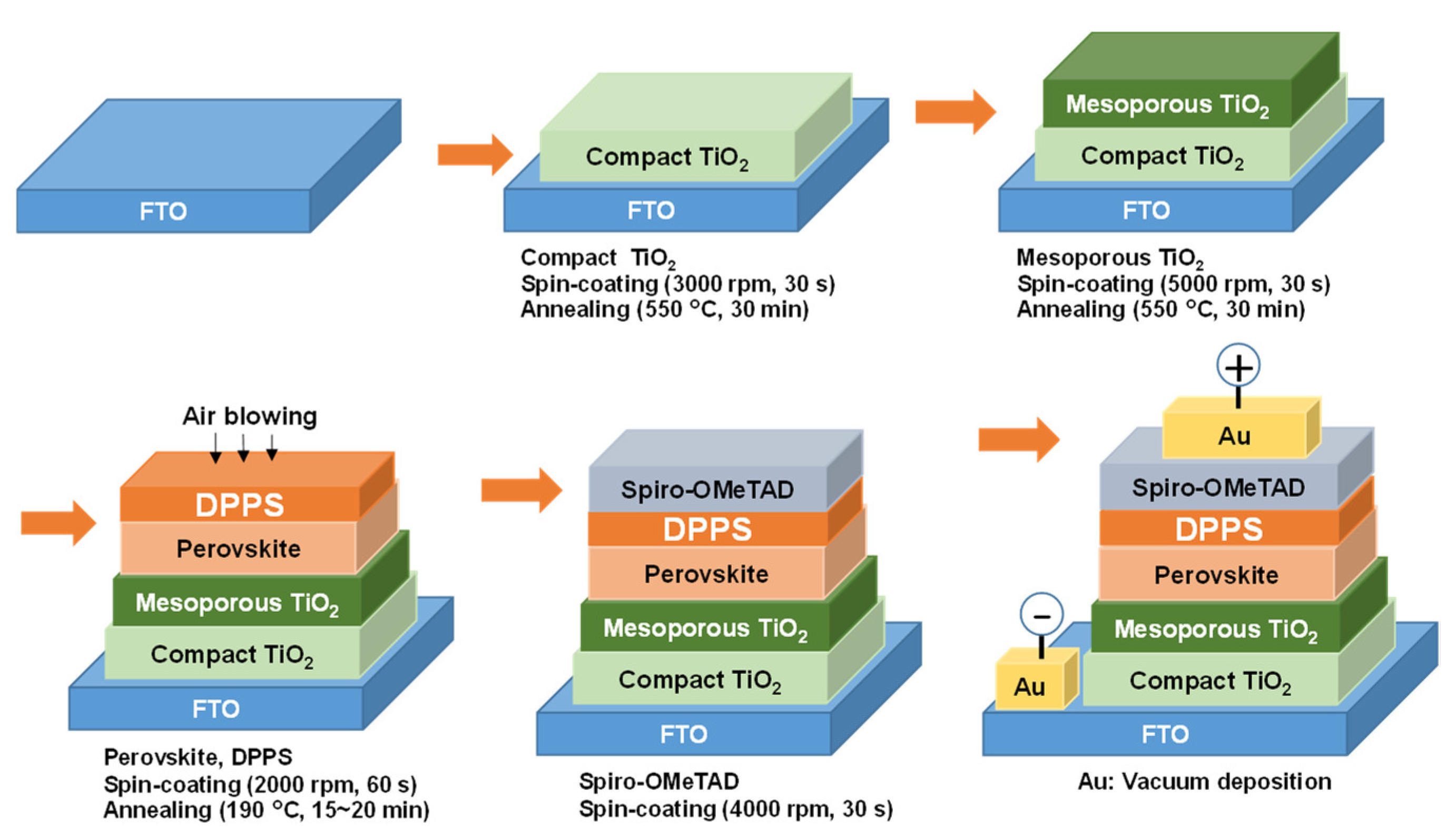
2. Materials and Methods
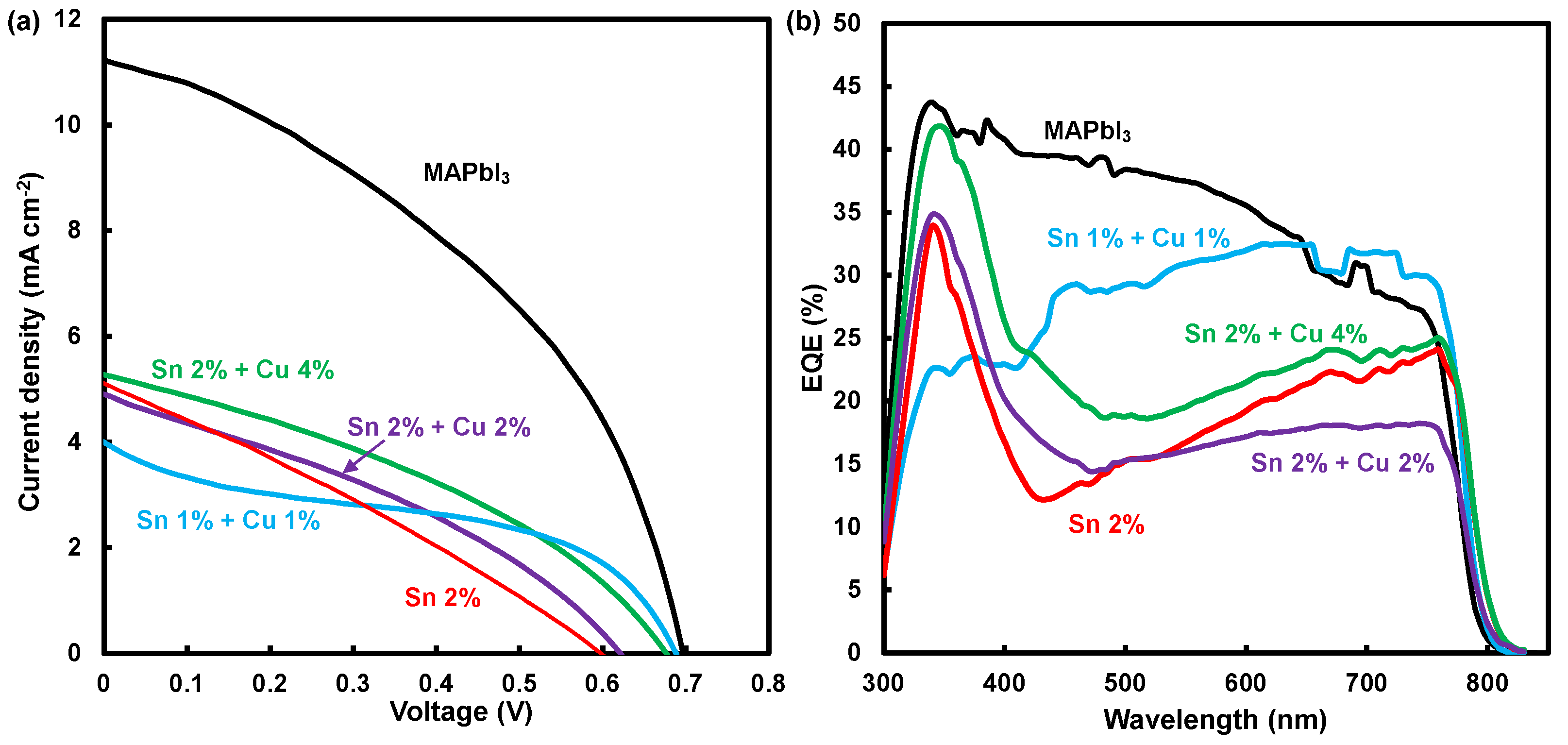
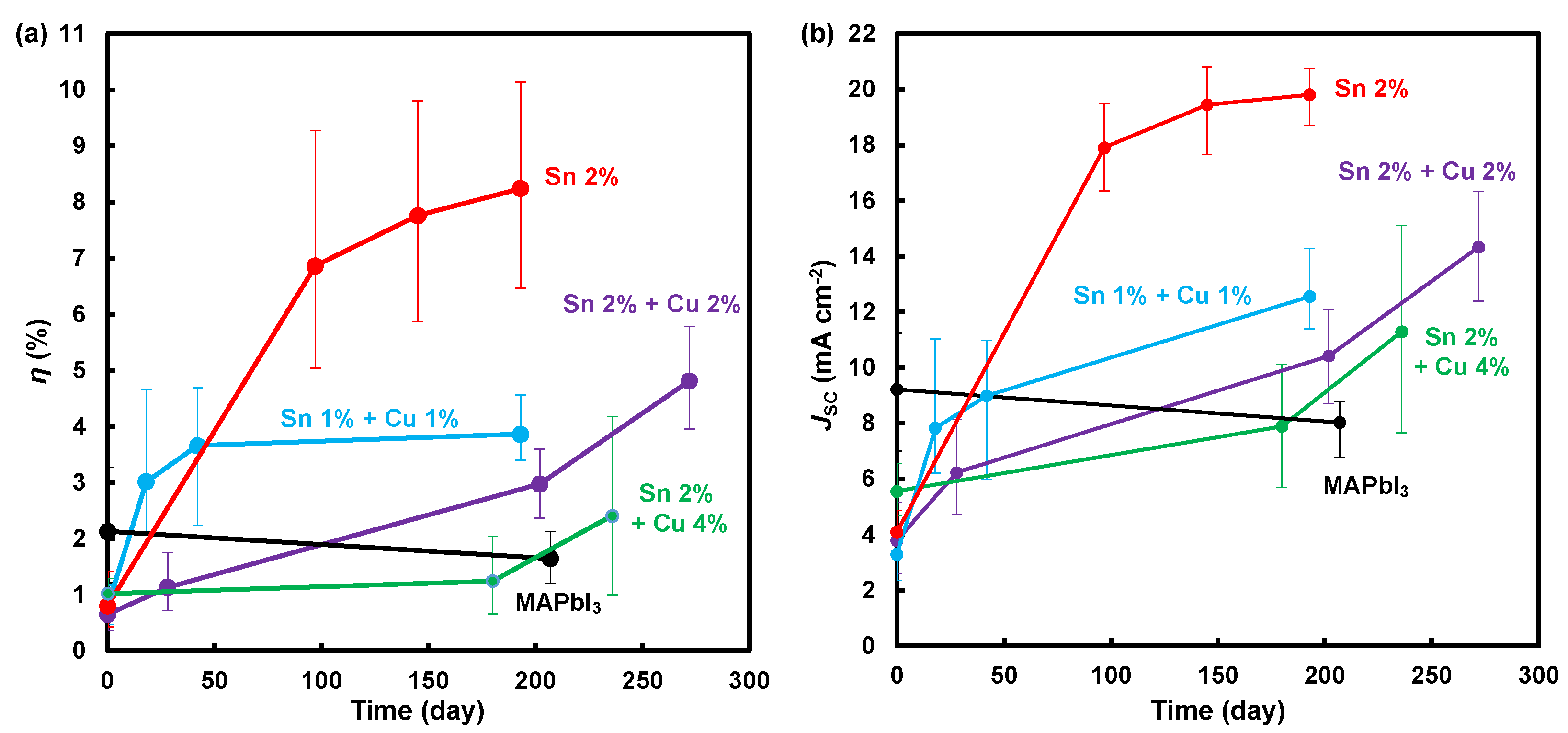
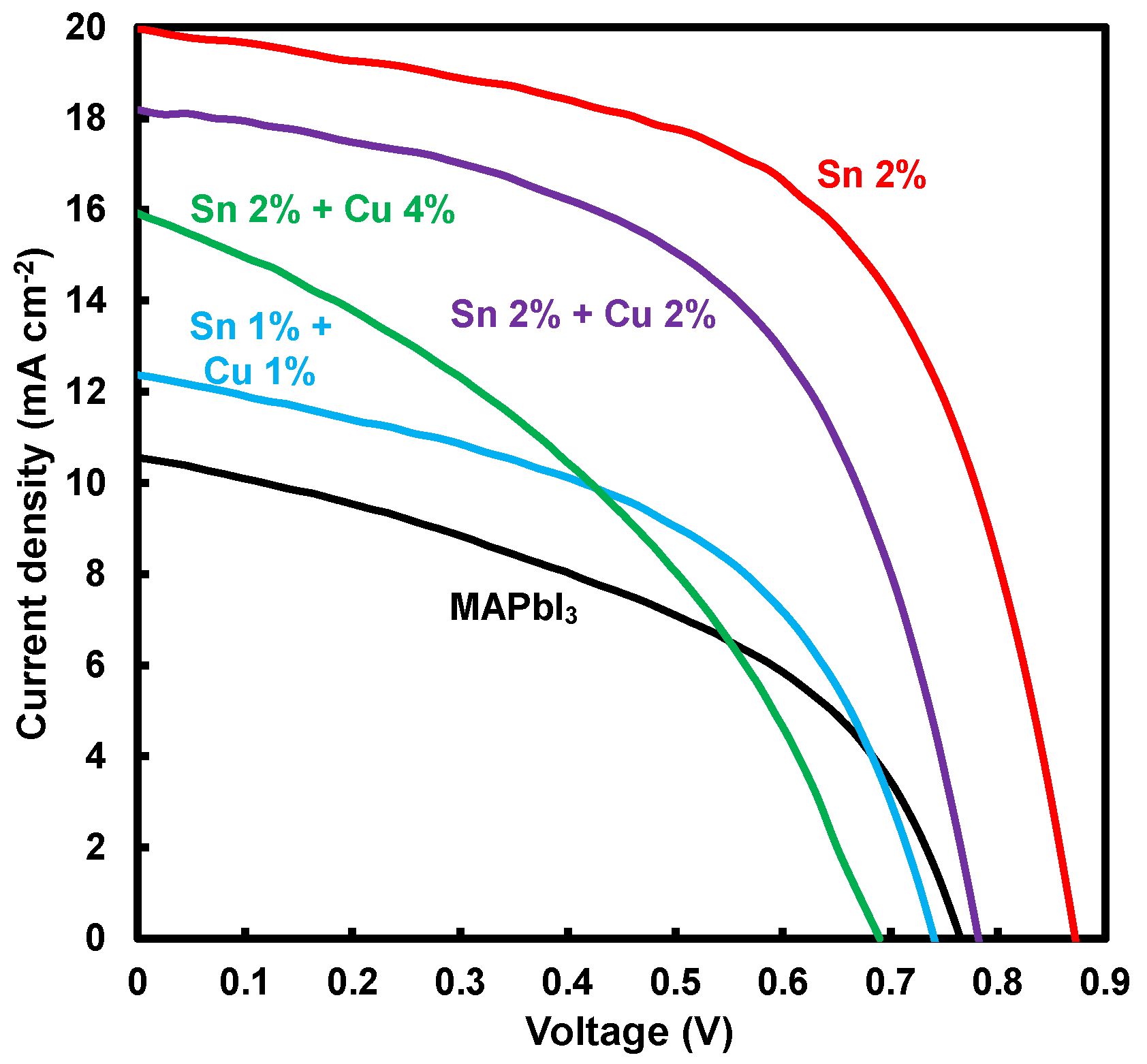
3. Results and Discussion
4. Conclusions
Author Contributions
Funding
Institutional Review Board Statement
Informed Consent Statement
Data Availability Statement
Conflicts of Interest
References
- Zhou, H.; Chen, Q.; Li, G.; Luo, S.; Song, T.B.; Duan, H.S.; Hong, Z.; You, J.; Liu, Y.; Yang, Y. Interface engineering of highly efficient perovskite solar cells. Science 2014, 345, 542–546. [Google Scholar] [CrossRef] [PubMed]
- Miyasaka, T. Perovskite photovoltaics: Rare functions of organo lead halide in solar cells and optoelectronic devices. Chem. Lett. 2015, 44, 720. [Google Scholar] [CrossRef] [Green Version]
- Saliba, M.; Orlandi, S.; Matsui, T.; Aghazada, S.; Cavazzini, M.; Correa-Baena, J.-P.; Gao, P.; Scopelliti, R.; Mosconi, E.; Dahmen, K.H.; et al. A molecularly engineered hole-transporting material for efficient perovskite solar cells. Nat. Energy 2016, 1, 15017. [Google Scholar] [CrossRef]
- Li, X.; Bi, D.; Yi, C.; Décoppet, J.D.; Luo, J.; Zakeeruddin, S.M.; Hagfeldt, A.; Grätzel, M. A vacuum flash–assisted solution process for high-efficiency large-area perovskite solar cells. Science 2016, 353, 58–62. [Google Scholar] [CrossRef] [PubMed]
- Chen, Z.; Turedi, B.; Alsalloum, A.Y.; Yang, C.; Zheng, X.; Gereige, I.; AlSaggaf, A.; Mohammed, O.F.; Bakr, O.M. Single-crystal MAPbI3 perovskite solar cells exceeding 21% power conversion efficiency. ACS Energy Lett. 2019, 4, 1258–1259. [Google Scholar] [CrossRef] [Green Version]
- Lee, J.; Baik, S. Enhanced crystallinity of CH3NH3PbI3 by the pre-coordination of PbI2–DMSO powders for highly reproducible and efficient planar heterojunction perovskite solar cells. RSC Adv. 2018, 8, 1005–1013. [Google Scholar] [CrossRef] [Green Version]
- Eze, V.O.; Lei, B.; Mori, T. Air-assisted flow and two-step spin-coating for highly efficient CH3NH3PbI3 perovskite solar cells. Jpn. J. Appl. Phys. 2016, 55, 02BF08. [Google Scholar] [CrossRef]
- Nishi, K.; Oku, T.; Kishimoto, T.; Ueoka, N.; Suzuki, A. Photovoltaic Characteristics of CH3NH3PbI3 Perovskite Solar Cells Added with Ethylammonium Bromide and Formamidinium Iodide. Coatings 2020, 10, 410. [Google Scholar] [CrossRef] [Green Version]
- Dunfield, S.P.; Bliss, L.; Zhang, F.; Luther, J.M.; Zhu, K.; van Hest, M.F.A.M.; Reese, M.O.; Berry, J.J. From defects to degradation: A mechanistic understanding of degradation in perovskite solar cell devices and modules. Adv. Energy Mater. 2020, 10, 1904054. [Google Scholar] [CrossRef]
- Lee, J.W.; Kim, S.G.; Yang, J.M.; Yang, Y.; Park, N.G. Verification and mitigation of ion migration in perovskite solar cells. APL Mater. 2019, 7, 041111. [Google Scholar] [CrossRef]
- Shi, Z.; Guo, J.; Chen, Y.; Li, Q.; Pan, Y.; Zhang, H.; Xia, Y.; Huang, W. Lead-free organic–inorganic hybrid perovskites for photovoltaic applications: Recent advances and perspectives. Adv. Mater. 2017, 29, 1605005. [Google Scholar] [CrossRef]
- Saliba, M.; Matsui, T.; Seo, J.Y.; Domanski, K.; Baena, J.P.C.; Nazeeruddin, M.K.; Zakeeruddin, S.M.; Tress, W.; Abate, A.; Hagfeldt, A.; et al. Cesium-containing triple cation perovskite solar cells: Improved stability, reproducibility and high efficiency. Energy Environ. Sci. 2016, 9, 1989–1997. [Google Scholar] [CrossRef] [Green Version]
- Yu, Y.; Wang, C.; Grice, C.R.; Shrestha, N.; Chen, J.; Zhao, D.; Liao, W.; Cimaroli, A.J.; Roland, P.J.; Ellingson, R.J.; et al. Improving the performance of formamidinium and cesium lead triiodide perovskite solar cells using lead thiocyanate additives. ChemSusChem 2016, 9, 3288–3297. [Google Scholar] [CrossRef]
- Oku, T. Crystal structures of perovskite halide compounds used for solar cells. Rev. Adv. Mater. Sci. 2020, 59, 264–305. [Google Scholar] [CrossRef]
- Wang, Y.; Dar, M.I.; Ono, L.K.; Zhang, T.; Kan, M.; Li, Y.; Zhang, L.; Wang, X.; Yang, Y.; Gao, X.; et al. Thermodynamically stabilized β-CsPbI3–based perovskite solar cells with efficiencies >18%. Science 2019, 365, 591–595. [Google Scholar] [CrossRef]
- McMeekin, D.P.; Sadoughi, G.; Rehman, W.; Eperon, G.E.; Saliba, M.; Hörantner, M.T.; Haghighirad, A.; Sakai, N.; Korte, L.; Rech, B.; et al. A mixed-cation lead mixed-halide perovskite absorber for tandem solar cells. Science 2016, 351, 151–155. [Google Scholar] [CrossRef] [Green Version]
- Oku, T.; Ohishi, Y.; Suzuki, A. Effects of antimony addition to perovskite-type CH3NH3PbI3 photovoltaic devices. Chem. Lett. 2016, 45, 134–136. [Google Scholar] [CrossRef] [Green Version]
- Suzuki, A.; Kishimoto, K.; Oku, T.; Okita, M.; Fukunishi, S.; Tachikawa, T. Additive effect of lanthanide compounds into perovskite layer on photovoltaic properties and electronic structures. Synth. Met. 2022, 287, 117092. [Google Scholar] [CrossRef]
- Enomoto, A.; Suzuki, A.; Oku, T.; Okita, M.; Fukunishi, S.; Tachikawa, T.; Hasegawa, T. Effects of Cu, K and guanidinium addition to CH3NH3PbI3 perovskite solar cells. J. Electron. Mater. 2022, 51, 4317–4328. [Google Scholar] [CrossRef]
- Okumura, R.; Oku, T.; Suzuki, A.; Okita, M.; Fukunishi, S.; Tachikawa, T.; Hasegawa, T. Effects of adding alkali metals and organic cations to Cu-based perovskite solar cells. Appl. Sci. 2022, 12, 1710. [Google Scholar] [CrossRef]
- Zhao, Y.; Tan, H.; Yuan, H.; Yang, Z.; Fan, J.Z.; Kim, J.; Voznyy, O.; Gong, X.; Quan, L.N.; Tan, C.S.; et al. Perovskite seeding growth of formamidinium-lead iodide-based perovskites for efficient and stable solar cells. Nat. Commun. 2018, 9, 1607. [Google Scholar] [CrossRef] [Green Version]
- Adjokatse, S.; Kardula, J.; Fang, H.H.; Shao, S.; ten Brink, G.H.; Loi, M.A. Effect of the device architecture on the performance of FA0.85MA0.15PbBr0.45I2.55 planar perovskite solar cells. Adv. Mater. Interfaces 2019, 6, 1801667. [Google Scholar] [CrossRef] [Green Version]
- Yan, W.; Rao, H.; Wei, C.; Liu, Z.; Bian, Z.; Xin, H.; Huang, W. Highly efficient and stable inverted planar solar cells from (FAI)x(MABr)1−xPbI2 perovskites. Nano Energy 2017, 35, 62–70. [Google Scholar] [CrossRef]
- Tosado, G.A.; Zheng, E.; Yu, Q. Tuning cesium–guanidinium in formamidinium tin triiodide perovskites with an ethylenediammonium additive for efficient and stable lead-free perovskite solar cells. Mater. Adv. 2020, 1, 3507–3517. [Google Scholar] [CrossRef]
- Kandori, S.; Oku, T.; Nishi, K.; Kishimoto, T.; Ueoka, N.; Suzuki, A. Fabrication and characterization of potassium- and formamidinium-added perovskite solar cells. J. Ceram. Soc. Jpn. 2020, 128, 805. [Google Scholar] [CrossRef]
- Oku, T.; Kandori, S.; Taguchi, M.; Suzuki, A.; Okita, M.; Minami, S.; Fukunishi, S.; Tachikawa, T. Polysilane-inserted methylammonium lead iodide perovskite solar cells doped with formamidinium and potassium. Energies 2020, 13, 4776. [Google Scholar] [CrossRef]
- Suzuki, A.; Taguchi, M.; Oku, T.; Okita, M.; Minami, S.; Fukunishi, S.; Tachikawa, T. Additive effects of methyl ammonium bromide or formamidinium bromide in methylammonium lead iodide perovskite solar cells using decaphenylcyclopentasilane. J. Mater. Sci. Mater. Electron. 2021, 32, 26449–26464. [Google Scholar] [CrossRef]
- Maqsood, A.; Li, Y.; Meng, J.; Song, D.; Qiao, B.; Zhao, S.; Xu, Z. Perovskite solar cells based on compact, smooth FA0.1MA0.9PbI3 film with efficiency exceeding 22%. Nanoscale Res. Lett. 2020, 15, 89. [Google Scholar] [CrossRef] [Green Version]
- Li, M.; Wang, Z.K.; Zhuo, M.P.; Hu, Y.; Hu, K.H.; Ye, Q.Q.; Jain, S.M.; Yang, Y.G.; Gao, X.Y.; Liao, L.S. Pb–Sn–Cu ternary organometallic halide perovskite solar cells. Adv. Mater. 2018, 30, 1800258. [Google Scholar] [CrossRef]
- Isikgor, F.H.; Li, B.; Zhu, H.; Xu, Q.; Ouyang, J. High performance planar perovskite solar cells with a perovskite of mixed organic cations and mixed halides, MA1−xFAxPbI3−yCly. J. Mater. Chem. A 2016, 4, 12543–12553. [Google Scholar] [CrossRef]
- Elseman, A.M.; Shalan, A.E.; Sajid, S.; Rashad, M.M.; Hassan, A.M.; Li, M. Copper-substituted lead perovskite materials constructed with different halides for working (CH3NH3)2CuX4-based perovskite solar cells from experimental and theoretical view. ACS Appl. Mater. Interfaces 2018, 10, 11699–11707. [Google Scholar] [CrossRef] [PubMed]
- Ueoka, N.; Oku, T.; Suzuki, A.; Sakamoto, H.; Yamada, M.; Minami, S.; Miyauchi, S. Fabrication and characterization of CH3NH3(Cs)Pb(Sn)I3(Cl) perovskite solar cells with TiO2 nanoparticle layers. Jpn. J. Appl. Phys. 2018, 57, 02CE03. [Google Scholar] [CrossRef]
- Hao, F.; Stoumpos, C.C.; Cao, D.H.; Chang, R.P.H.; Kanatzidis, M.G. Lead-free solid-state organic–inorganic halide perovskite solar cells. Nat. Photonics 2014, 8, 489–494. [Google Scholar] [CrossRef]
- Ueoka, N.; Oku, T.; Suzuki, A. Additive effects of alkali metals on Cu-modified CH3NH3PbI3−δClδ photovoltaic devices. RSC Adv. 2019, 9, 24231. [Google Scholar] [CrossRef] [PubMed] [Green Version]
- Ueoka, N.; Oku, T. Effects of co-addition of sodium chloride and copper(ii) bromide to mixed-cation mixed-halide perovskite photovoltaic devices. ACS Appl. Energy Mater. 2020, 9, 24231. [Google Scholar] [CrossRef]
- Ueoka, N.; Oku, T.; Suzuki, A. Effects of doping with Na, K, Rb, and formamidinium cations on (CH3NH3)0.99Rb0.01Pb0.99Cu0.01I3−x(Cl, Br)x perovskite photovoltaic cells. AIP Adv. 2020, 10, 125023. [Google Scholar] [CrossRef]
- Oku, T.; Ohishi, Y.; Ueoka, N. Highly (100)-oriented CH3NH3PbI3(Cl) perovskite solar cells prepared with NH4Cl using an air blow method. RSC Adv. 2018, 8, 10389–10395. [Google Scholar] [CrossRef] [Green Version]
- Oku, T.; Ohishi, Y. Effects of annealing on CH3NH3PbI3 (Cl) perovskite photovoltaic devices. J. Ceram. Soc. Jpn. 2018, 126, 56–60. [Google Scholar] [CrossRef] [Green Version]
- Taguchi, M.; Suzuki, A.; Oku, T.; Ueoka, N.; Minami, S.; Okita, M. Effects of annealing temperature on decaphenylcyclopentasilane-inserted CH3NH3PbI3 perovskite solar cells. Chem. Phys. Lett. 2019, 737, 136822. [Google Scholar] [CrossRef]
- Oku, T.; Taguchi, M.; Suzuki, A.; Kitagawa, K.; Asakawa, Y.; Yoshida, S.; Okita, M.; Minami, S.; Fukunishi, S.; Tachikawa, T. Effects of polysilane addition to chlorobenzene and high temperature annealing on CH3NH3PbI3 perovskite photovoltaic devices. Coatings 2021, 11, 665. [Google Scholar] [CrossRef]
- Suzuki, A.; Kato, M.; Ueoka, N.; Oku, T. Additive effect of formamidinium chloride in methylammonium lead halide compound-based perovskite solar cells. J. Electron. Mater. 2019, 48, 3900–3907. [Google Scholar] [CrossRef]
- Oku, T.; Zushi, M.; Imanishi, Y.; Suzuki, A.; Suzuki, K. Microstructures and photovoltaic properties of perovskite-type CH3NH3PbI3 compounds. Appl. Phys. Express 2014, 7, 121601. [Google Scholar] [CrossRef]
- Jokar, E.; Chien, C.H.; Tsai, C.M.; Fathi, A.; Diau, E.W.G. Robust tin-based perovskite solar cells with hybrid organic cations to attain efficiency approaching 10%. Adv. Mater. 2019, 37, 1804835. [Google Scholar] [CrossRef] [PubMed]
- Kim, G.; Min, H.; Lee, K.S.; Lee, D.Y.; Yoon, S.M.; Seok, S.I. Impact of strain relaxation on performance of α-formamidinium lead iodide perovskite solar cells. Science 2020, 370, 108–112. [Google Scholar] [CrossRef]
- Yang, W.S.; Park, B.W.; Jung, E.H.; Jeon, N.J.; Kim, Y.C.; Lee, D.U.; Shin, S.S.; Seo, J.; Kim, E.K.; Noh, J.H.; et al. Iodide management in formamidinium-lead-halide–based perovskite layers for efficient solar cells. Science 2017, 356, 1376–1379. [Google Scholar] [CrossRef] [Green Version]
- Konstantakou, M.; Stergiopoulos, T. A critical review on tin halide perovskite solar cells. J. Mater. Chem. A 2017, 5, 11518–11549. [Google Scholar] [CrossRef]
- Ferdani, D.W.; Pering, S.R.; Ghosh, D.; Kubiak, P.; Walker, A.B.; Lewis, S.E.; Johnson, A.L.; Baker, P.J.; Islam, M.S.; Cameron, P.J. Partial cation substitution reduces iodide ion transport in lead iodide perovskite solar cells. Energy Environ. Sci. 2019, 12, 2264–2272. [Google Scholar] [CrossRef] [Green Version]
- Osherov, A.; Feldman, Y.; Ashiri, I.K.; Cahen, D.; Hodes, G. Halide diffusion in MAPbX3: Limits to topotaxy for halide exchange in perovskites. Chem. Mater. 2020, 32, 4223–4231. [Google Scholar] [CrossRef]
- Eames, C.; Frost, J.M.; Barnes, P.R.F.; O’Regan, B.C.; Walsh, A.; Islam, M.S. Ionic transport in hybrid lead iodide perovskite solar cells. Nat. Commun. 2015, 6, 7497. [Google Scholar] [CrossRef] [Green Version]
- Suzuki, A.; Oe, M.; Oku, T. Fabrication and characterization of Ni-, Co-, and Rb-incorporated CH3NH3PbI3 perovskite solar cells. J. Electron. Mater. 2021, 50, 1980–1995. [Google Scholar] [CrossRef]
- Suzuki, A.; Oku, T. Effects of mixed-valence states of Eu-doped FAPbI3 perovskite crystals studied by first-principles calculation. Mater. Adv. 2021, 2, 2609–2616. [Google Scholar] [CrossRef]
- Suzuki, A.; Kitagawa, K.; Oku, T.; Okita, M.; Fukunishi, S.; Tachikawa, T. Additive effects of copper and alkali metal halides into methylammonium lead iodide perovskite solar cells. Electron. Mater. Lett. 2022, 18, 176–186. [Google Scholar] [CrossRef]
- Kishimoto, T.; Oku, T.; Suzuki, A.; Ueoka, N. Additive effects of guanidinium iodide on CH3NH3PbI3 perovskite solar cells. Phys. Status Solidi A 2021, 218, 2100396. [Google Scholar] [CrossRef]
- Ono, I.; Oku, T.; Suzuki, A.; Asakawa, Y.; Terada, S.; Okita, M.; Fukunishi, S.; Tachikawa, T. Fabrication and characterization of CH3NH3PbI3 solar cells with added guanidinium and inserted with decaphenylpentasilane. Jpn. J. Appl. Phys. 2022, 61, SB1024. [Google Scholar] [CrossRef]
- Terada, S.; Oku, T.; Suzuki, A.; Okita, M.; Fukunishi, S.; Tachikawa, T.; Hasegawa, T. Ethylammonium bromide- and potassium-added CH3NH3PbI3 perovskite solar cells. Photonics 2022, 9, 791. [Google Scholar] [CrossRef]


| Device Notation | Sn (%) | Cu (%) | t-Factor |
|---|---|---|---|
| Standard | 0 | 0 | 0.9115 |
| Sn 2% | 2 | 0 | 0.9209 |
| Sn 1% + Cu 1% | 1 | 1 | 0.9213 |
| Sn 2% + Cu 2% | 2 | 2 | 0.9235 |
| Sn 2% + Cu 4% | 2 | 4 | 0.9262 |
| Device | JSC (mA cm−2) | VOC (V) | FF | RS (Ω cm2) | RSh (Ω cm2) | η (%) | ηave (%) | Eg (eV) |
|---|---|---|---|---|---|---|---|---|
| Standard | 11.2 | 0.696 | 0.419 | 16.2 | 217 | 3.28 | 2.13 | 1.57 |
| Sn 2% | 5.12 | 0.598 | 0.287 | 68.7 | 149 | 0.879 | 0.546 | 1.54 |
| Sn 1% + Cu 1% | 4.00 | 0.688 | 0.427 | 24.8 | 586 | 1.17 | 0.802 | 1.55 |
| Sn 2% + Cu 2% | 4.91 | 0.621 | 0.342 | 47.8 | 200 | 1.04 | 0.653 | 1.54 |
| Sn 2% + Cu 4% | 5.28 | 0.677 | 0.364 | 42.8 | 245 | 1.30 | 1.02 | 1.54 |
| Device | Time (Day) | JSC (mA cm−2) | VOC (V) | FF | RS (Ω cm2) | RSh (Ω cm2) | η (%) | ηave (%) |
|---|---|---|---|---|---|---|---|---|
| Standard | 0 | 11.2 | 0.696 | 0.419 | 16.2 | 217 | 3.28 | 2.13 |
| Sn 2% | 193 | 20.0 | 0.871 | 0.583 | 6.14 | 323 | 10.14 | 8.24 |
| Sn 1% + Cu 1% | 193 | 12.4 | 0.740 | 0.499 | 9.38 | 217 | 4.56 | 3.86 |
| Sn 2% + Cu 2% | 386 | 18.2 | 0.781 | 0.550 | 7.36 | 345 | 7.81 | 7.23 |
| Sn 2% + Cu 4% | 236 | 15.1 | 0.712 | 0.389 | 16.9 | 107 | 4.17 | 2.77 |
| Device | Time (Day) | JSC (mA cm−2) | VOC (V) | FF | RS (Ω cm2) | RSh (Ω cm2) | η (%) | ηave (%) |
|---|---|---|---|---|---|---|---|---|
| Sn 2% | 817 | 16.3 | 0.823 | 0.514 | 4.61 | 287 | 6.90 | 6.55 |
| Sn 1% + Cu 1% | 818 | 6.57 | 0.747 | 0.541 | 2.56 | 442 | 2.65 | 2.44 |
| Sn 2% + Cu 2% | 680 | 15.8 | 0.761 | 0.587 | 3.35 | 375 | 7.04 | 6.34 |
| Sn 2% + Cu 4% | 660 | 14.1 | 0.471 | 0.270 | 4.95 | 37.8 | 1.79 | 1.38 |
| Device | Time (Day) | JSC (mA cm−2) | VOC (V) | FF | RS (Ω cm2) | RSh (Ω cm2) | η (%) | ηave (%) |
|---|---|---|---|---|---|---|---|---|
| Sn 5% | 0 | 3.00 | 0.704 | 0.344 | 65.7 | 357 | 0.724 | 0.432 |
| Sn 5% | 83 | 8.17 | 0.894 | 0.560 | 10.3 | 613 | 4.10 | 3.25 |
| Sn 5% | 115 | 11.60 | 0.922 | 0.577 | 7.53 | 564 | 6.16 | 5.84 |
| Sn 5% + Cu 5% | 0 | 1.82 | 0.360 | 0.322 | 67.8 | 420 | 0.211 | 0.170 |
| Sn 5% + Cu 5% | 76 | 11.6 | 0.750 | 0.457 | 13.1 | 192 | 3.96 | 2.84 |
| Sn 5% + Cu 5% | 115 | 10.75 | 0.788 | 0.384 | 22.7 | 229 | 3.25 | 2.88 |
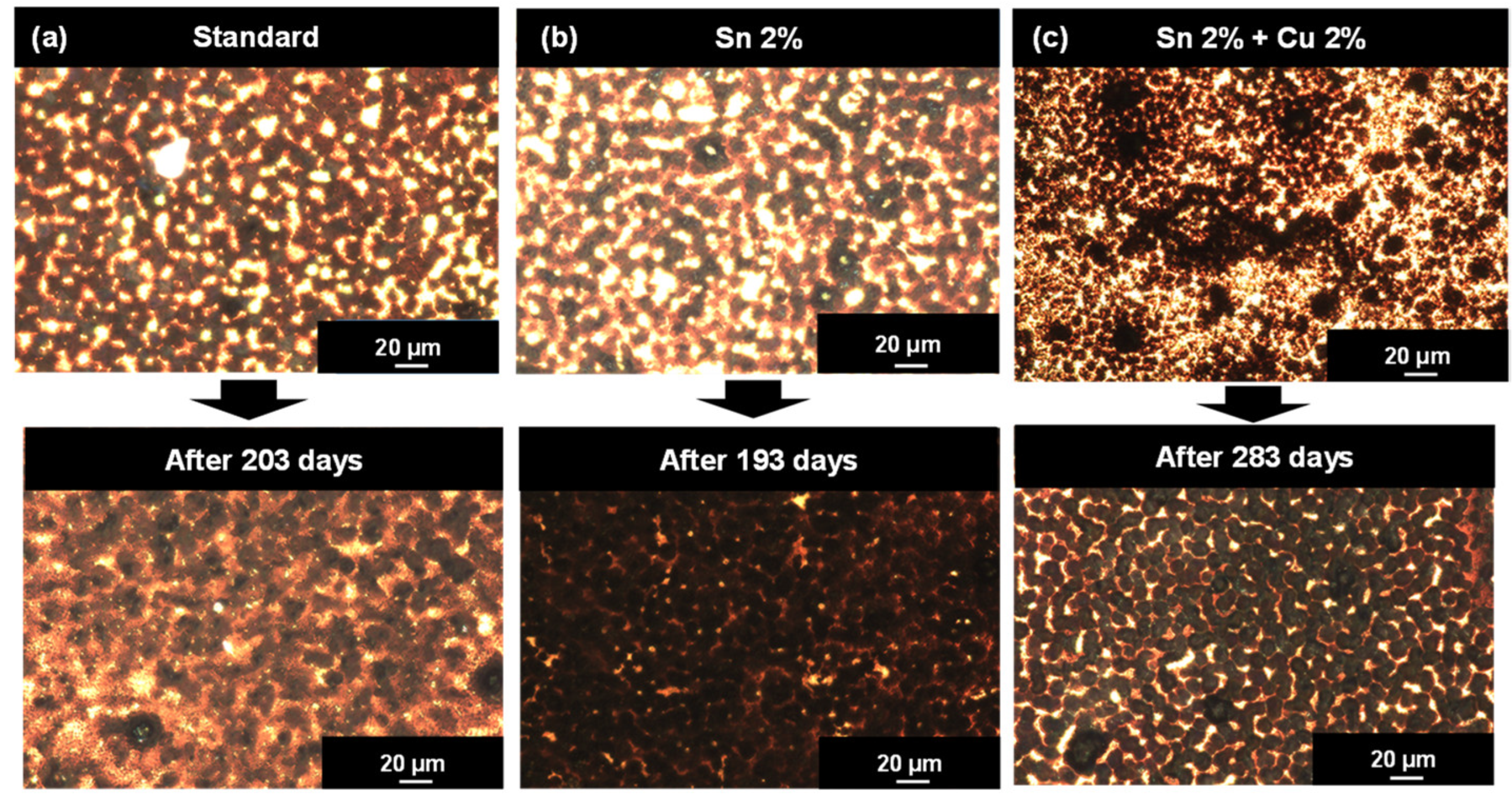
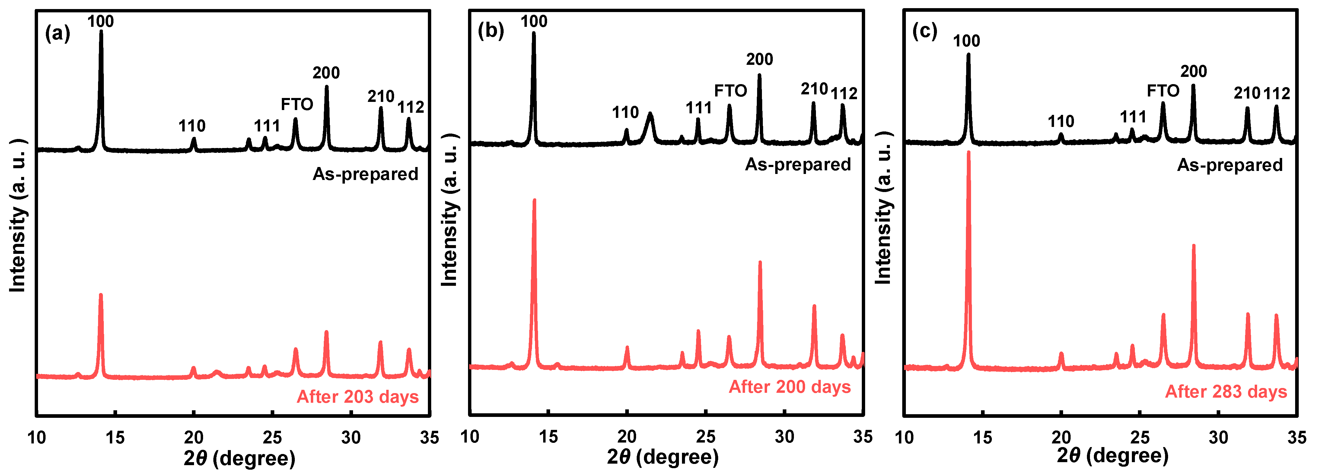
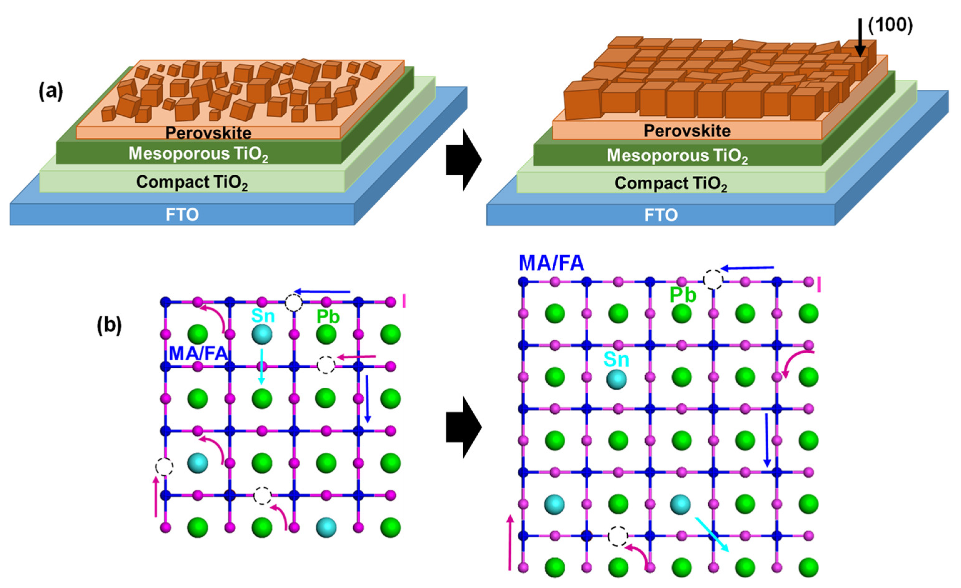
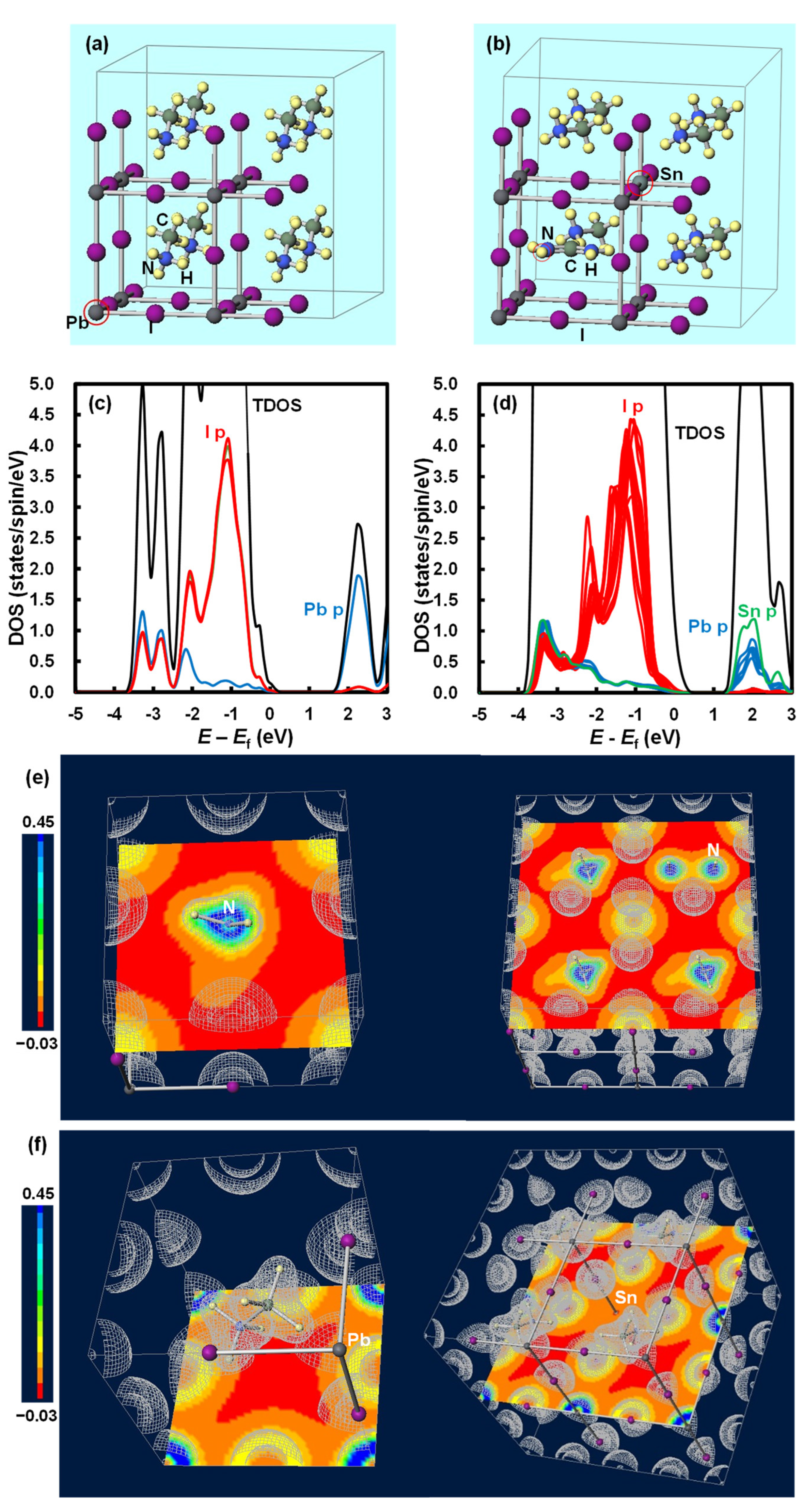
| Device | Time (Days) | Lattice Constant (Å) | I100/I210 | Grain Size (μm) | Coverage (%) | K (10−19 m2 s−1) |
|---|---|---|---|---|---|---|
| Standard | 0 | 6.271(1) | 2.5 | 6.77 | 75.6 | |
| 203 | 6.269(1) | 2.1 | 6.46 | 68.0 | −2.34 | |
| Sn 2% | 0 | 6.280(1) | 2.4 | 5.45 | 67.9 | |
| 193 | 6.270(1) | 2.6 | 7.68 | 93.3 | 17.6 | |
| Sn 2% + Cu 2% | 0 | 6.282(1) | 2.3 | 5.06 | 75.5 | |
| 283 | 6.277(0) | 3.7 | 7.57 | 86.7 | 13.0 |
Publisher’s Note: MDPI stays neutral with regard to jurisdictional claims in published maps and institutional affiliations. |
© 2022 by the authors. Licensee MDPI, Basel, Switzerland. This article is an open access article distributed under the terms and conditions of the Creative Commons Attribution (CC BY) license (https://creativecommons.org/licenses/by/4.0/).
Share and Cite
Asakawa, Y.; Oku, T.; Kido, M.; Suzuki, A.; Okumura, R.; Okita, M.; Fukunishi, S.; Tachikawa, T.; Hasegawa, T. Fabrication and Characterization of SnCl2- and CuBr-Added Perovskite Photovoltaic Devices. Technologies 2022, 10, 112. https://doi.org/10.3390/technologies10060112
Asakawa Y, Oku T, Kido M, Suzuki A, Okumura R, Okita M, Fukunishi S, Tachikawa T, Hasegawa T. Fabrication and Characterization of SnCl2- and CuBr-Added Perovskite Photovoltaic Devices. Technologies. 2022; 10(6):112. https://doi.org/10.3390/technologies10060112
Chicago/Turabian StyleAsakawa, Yugo, Takeo Oku, Masashi Kido, Atsushi Suzuki, Riku Okumura, Masanobu Okita, Sakiko Fukunishi, Tomoharu Tachikawa, and Tomoya Hasegawa. 2022. "Fabrication and Characterization of SnCl2- and CuBr-Added Perovskite Photovoltaic Devices" Technologies 10, no. 6: 112. https://doi.org/10.3390/technologies10060112