Article

Design of True Time Delay Millimeter Wave Beamformers for 5G Multibeam Phased Arrays

by
Dimitrios I. Lialios
1,
Nikolaos Ntetsikas
2,
Konstantinos D. Paschaloudis
2,
Constantinos L. Zekios
1,*,
Stavros V. Georgakopoulos
1 and
George A. Kyriacou
2,*
1
College of Engineering & Computing, Florida International University, Miami, FL 33174, USA
2
Department of Electrical & Computer Engineering, Democritus University of Thrace, 67100 Xanthi, Greece
*
Authors to whom correspondence should be addressed.
Electronics 2020, 9(8), 1331; https://doi.org/10.3390/electronics9081331
Submission received: 15 July 2020 / Revised: 6 August 2020 / Accepted: 10 August 2020 / Published: 18 August 2020

Abstract

:
Millimeter wave (mm-Wave) technology is likely the key enabler of 5G and early 6G wireless systems. The high throughput, high capacity, and low latency that can be achieved, when mm-Waves are utilized, makes them the most promising backhaul as well as fronthaul solutions for the communication between small cells and base stations or between base stations and the gateway. Depending on the channel properties different communication systems (e.g., beamforming and MIMO) can accordingly offer the best solution. In this work, our goal is to design millimeter wave beamformers for switched beam phased arrays as hybrid beamforming stages. Specifically, three different analog beamforming techniques for the frequency range of 27–33 GHz are presented. First, a novel compact multilayer Blass matrix is proposed. Second, a modified dummy-ports free, highly efficient Rotman lens is introduced. Finally, a three-layer true-time-delay tree topology inspired by microwave photonics is presented.

1. Introduction

The evolution of fifth generation (5G) wireless systems toward high microwave and millimeter wave (mm-Wave) frequencies provides significant advantages because of the wide available spectrum (i.e., high throughput, high capacity, and low latency) and improved features resulting from the smaller wavelength [1,2,3,4,5,6,7,8,9,10,11,12]. Of course, higher frequencies are characterized by challenges of higher propagation losses, higher phase noise in local oscillators, and higher insertion loss in the RF-front-end. This is accompanied by possible shadowing even by trees, limited propagation range due to rain attenuation, atmospheric and molecular absorption, and lower or impossible penetration to buildings [13,14,15,16]. The latter can be compensated by ensuring line-of-sight links, thereby requiring dense base stations even down to distances of 150–200 m [17]. Therefore, mm-Wave communications are mainly used for indoor environments and small cell access. This densification is anyways needed to ensure the excessively high communication rates of 5G. Of course, densely deployed small cells demand high cost to connect 5G base stations (BSs) to other BSs and to the network by fiber-based backhaul [18]. In contrast, wireless backhaul in mm-Wave bands that offers high speed, wide bandwidth, several G b p s data rates is by far more cost-effective, flexible and much easier to deploy. As shown in Figure 1, a wireless mm-Wave communication system is an extremely promising backhaul solution for small cells that can support the desired high speed transmission between the small cell base stations (BSs) or between BSs and the gateway. However, high antenna gain (or narrow beamwidth) is needed to compensate for high propagation losses; therefore, beamforming is required.
Besides beamforming, antenna diversity (two or more antennas at different positions) has been used at low microwave frequencies (i.e., below 6 GHz) to compensate the effects of multipath propagation. Even though multipath effects are negligible at millimeter waves or above 7 GHz ( F R 3 band) as they require line–of–sight paths, antenna diversity is still beneficial at these frequencies. Specifically, it has been shown that the capacity of communication systems at these frequencies can be increased by employing multiple antennas (i.e., MIMO) to receive signals. A MIMO configuration can be deployed in single-user systems, where it offers the best throughput, or for multi-user systems to increase the overall cell capacity. On the other hand, beamforming needs antenna elements with the same polarization. A beam can be made directive even with two antenna elements, but with very poor results. Instead, four antennas offer acceptable directivity, while eight antennas provide the best compromise [e.g., especially for the 7–24 GHz ( F R 3 range)]. Additionally, it has been shown that beamforming is more efficient than MIMO in hard–to–cover areas (cell edges or through buildings) where the SNR is low [19]. On the contrary, MIMO is more efficient than beamforming in areas with strong S N R (best for S N R > 17 dB), i.e., near the center of a cell, where multiple layers of MIMO are used. Therefore, the most practically feasible configuration of a passive antenna at frequencies below 6 GHz, is one that implements both beamforming and MIMO operations. The established configuration, which incorporates both beamforming and MIMO, is known as “Hybrid Beamforming’’ and it is generally accepted as the best option for the upper microwave (7–33 GHz) and millimeter wave bands [20,21,22,23].
Hybrid beamforming has been adopted since 1970. In addition, various hybrid beamforming systems have been presented in recent papers (e.g., [22,24]). Specifically, such systems are comprised of the following components, as shown in Figure 2: (i) the antenna array; (ii) the “RF precoding”, i.e., the analog RF beamformer that is driven by a number of transmitting RF chains; and (iii) a number of digital–to–analog converters (DACs) that combine the “digital baseband precoding” (which plays the role of the software defined radio (SDR) for the transmitter) into the analog RF beamforming networks. The receiver follows the same logic and appears at the bottom of Figure 2. Notably, hybrid beamforming combines the low cost, simplicity, and ease of implementation of analog beamformers with powerful abilities of digital beamformers, such as comprehensive interference rejection and beamsteering towards any desired position (at least theoretically) [25]. Therefore, by combining the analog and digital beamformers, novel communication systems can be developed that meet the needs of 5G [26]. Our paper is focused on analogue beamformers that represent an important component of hybrid beamforming systems.
Many different analog RF beamforming implementations have been developed during the last 60 years following the topologies proposed by Butler [27], Blass [28], and Nolen [29] matrices, as well as Rotman lenses [30]. The most common analog beamforming network is based on the Butler matrix, which is known for its high efficiency. However, it can only produce uniform amplitude distributions that are known for their high side-lobe level ( S L L ) values [31], and high number of crossovers that cause many undesired effects, such as increased insertion loss, mismatched junctions, etc. [32]. In the literature, limited works have been proposed for the development of Butler matrices with non-uniform amplitude distributions [33] and the reduction of crossovers [34]. Additionally, Butler matrices exhibit significantly narrower bandwidths than the most wideband antenna arrays currently available. A design with bandwidth of 3:1 (based on a 10 d B return loss), 1 d B insertion loss variation, and 7 ° phase deviation was recently reported by Chen et al. [35]. Even though Butler matrices have been extensively used at the frequency range of 1–4 GHz, there are limited works at higher frequencies and mm-Waves. Nedil et al. [36] introduced a 4 × 4 two-layer Butler matrix at 5.8 GHz using coplanar wave-guide technology. Cao et al. [37], introduced a compact substrate integrated waveguide (SIW) multi-folded 4 × 8 Butler matrix combined with a 8 × 10 SIW slot-coupled patch array at 38 GHz accomplishing a size reduction of 53.5 % in its longitudinal direction. Tornielli di Crestvolant et al. [38] introduced a new class of Butler matrices with inherent bandpass filter transfer functions. Specifically, they presented the synthesis and design of a 2 × 2 , 180 hybrid coupler at 10 GHz and a 4 × 4 Butler matrix with an equal-ripple four-pole Chebyshev bandpass characteristic centered at 12.5 GHz. More recently Dyad et al. [39] presented a dually-polarized Butler matrix for base stations with polarization diversity operating at 60 GHz. Finally, Tamayo-Dominguez et al. [40] utilized additive manufacturing techniques to introduce a 3 D -printed modified butler matrix for a monopulse radar based on gap waveguides at W-Band.
Nolen matrices outperform Butler matrices as they can produce an arbitrary number of beams. However, similar to Butler matrices, they are usually limited to uniform amplitude tapering and only few reported attempts have attempted to fix this problem [41]. In addition, Nolen networks operate at relatively narrowband frequency range, compared to wideband antenna arrays. Djerafi et al. [42], introduced a relatively broadband Nolen matrix using substrate integrated waveguide (SIW) technology, which provided constant phase over a 11.7 % frequency bandwidth centered at 77 GHz. More recently, a Nolen matrix with slightly wider bandwidth of 1.4:1, amplitude imbalance less than 0.75 dB, phase variation 6 ° , and return loss better than 16 dB was proposed by Ren et al. [43].
The Blass matrix is the ordinary case of the Nolen matrix. In addition, the Blass matrix can provide non-uniform amplitudes (thereby overcoming Nolen matrix limitations for uniform amplitudes) but exhibits higher losses due to the use of matched loads. Moreover, the Blass matrix can be designed as a true time-delay network, thereby resolving (at least in theory) the bandwidth limitations of both Butler and Nolen matrices. A true time-delay Blass matrix with an instantaneous bandwidth of 5:1 was first reported by Chu et al. [44]. However, this was an active network design that used amplifiers as directional couplers.
Finally, Rotman lenses are passive topologies that have been used to implement true time-delay beamforming networks. The main advantage of Rotman lenses is that they require low number of switching elements, compared to Blass matrices. Rotman lenses have been extensively used with relatively wideband performance, such as 3.4:1 by Lambrecht et al. [45] and 10:1 by Merola et al. [46]. However, Rotman lenses suffer from relatively low efficiency (e.g., 20–50% efficiency was reported by Merola [46]).
In this work, three novel analog beamforming networks are proposed as 5G mm-wave candidates. Each network separately tackles and solves specific limitations and drawbacks of its prior counterparts. First, a multilayer Blass matrix design is presented. To our knowledge, this is the first multilayer, circular Blass topology. Typical Blass networks are big in size and suffer from excessive losses. Aiming towards compact and highly efficient mm-Wave beamforming networks, we first transform the classical Blass matrix topology [28] into a circular design [47], and then implement it in a two-layer topology. The challenge of this attempt is the appropriate design of the couplers. Typical approaches use bondwires and bridges [48], two factors that decrease the efficiency of beamformers and increase the design complexity. In this work, to minimize the losses and significantly reduce the design complexity, a dual-layer directional coupler is designed and used. As a proof of concept, a 3 × 4 Blass matrix is designed, which shows excellent performance. Compared to the typical single-layer Blass matrix the proposed dual-layer network achieves 60 % size reduction.
The second topology, which is presented here, is a modified Rotman lens topology. Rotman lenses, similar to the Blass matrix topologies have large footprints, while their efficiency is limited due to the existence of dummy ports. Aiming towards a compact, low cost and highly efficient design, we minimize the number of dummy ports by using field absorbers. Specifically, by imitating perfect matched layers (PMLs), we engineer the substrate by doping it with conductive material. This key modification essentially increases the loss tangent about ten times, yielding an almost perfect absorber and thereby eliminating the undesired reflections. As a proof of concept, a simple 3 × 3 structure, which shows very good results, is presented here.
Our last topology is a tree topology inspired by microwave photonics. Specifically, this implementation provides ultra-wideband operation; eliminates the problems of crossovers faced by Butler, Nolen, and Blass matrices; and is capable of providing significantly higher efficiencies than ordinary Rotman lenses. The primary novelty of this topology is the minimal number of delay lines. By hierarchically repeating the same feature, using successive power divisions (equal and un-equal) and by doubling the delay as we move diagonally from the first antenna port to its last port and towards the network input, we achieve the desired amplitude and phase difference. As a proof of concept, a three-layer 1 × 4 network, which shows excellent results, is designed.

2. Beamforming Networks Design

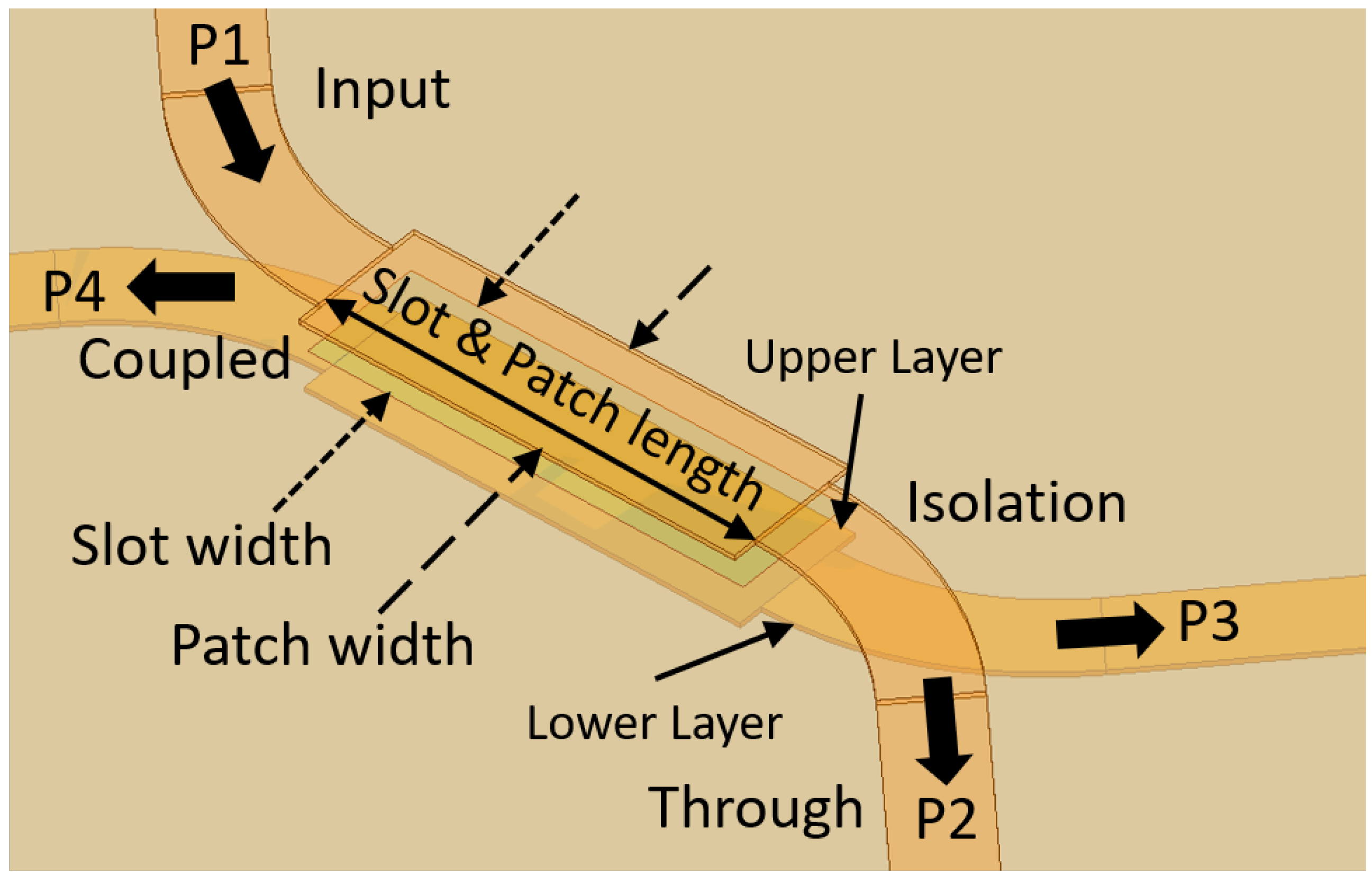
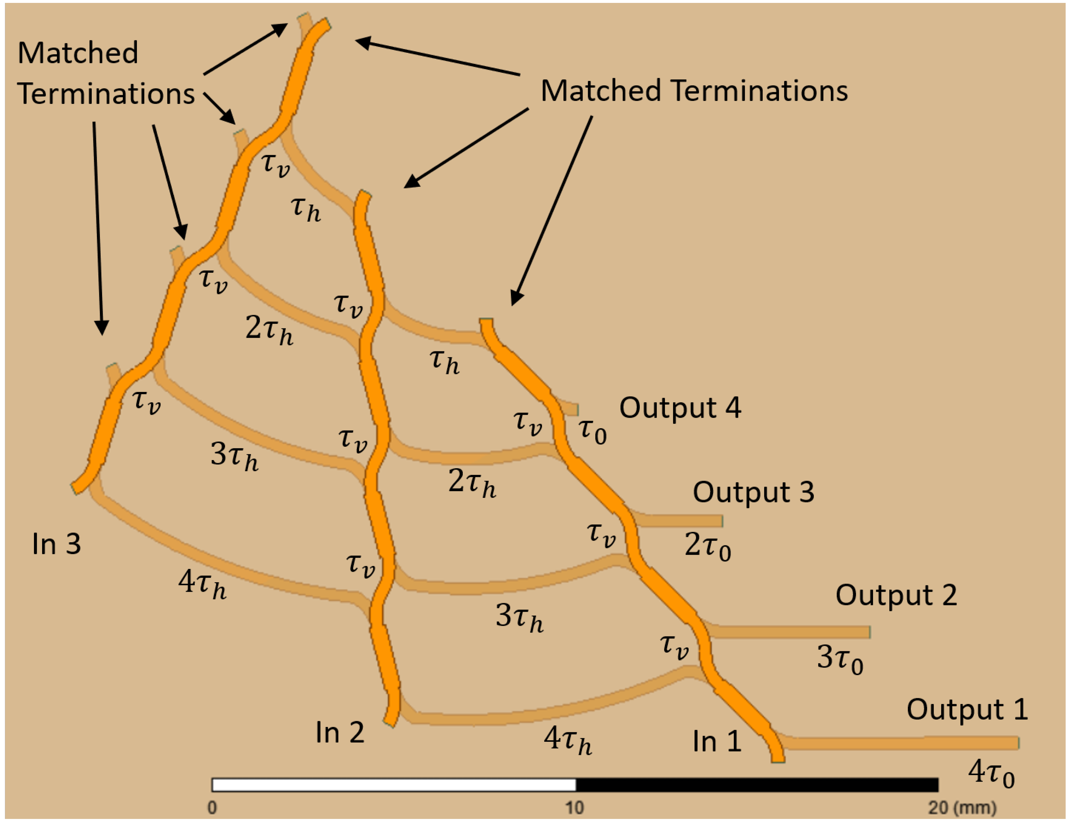
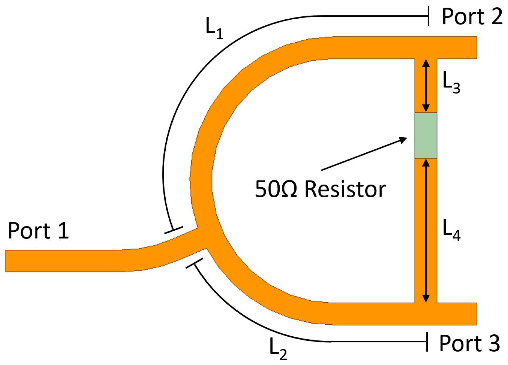
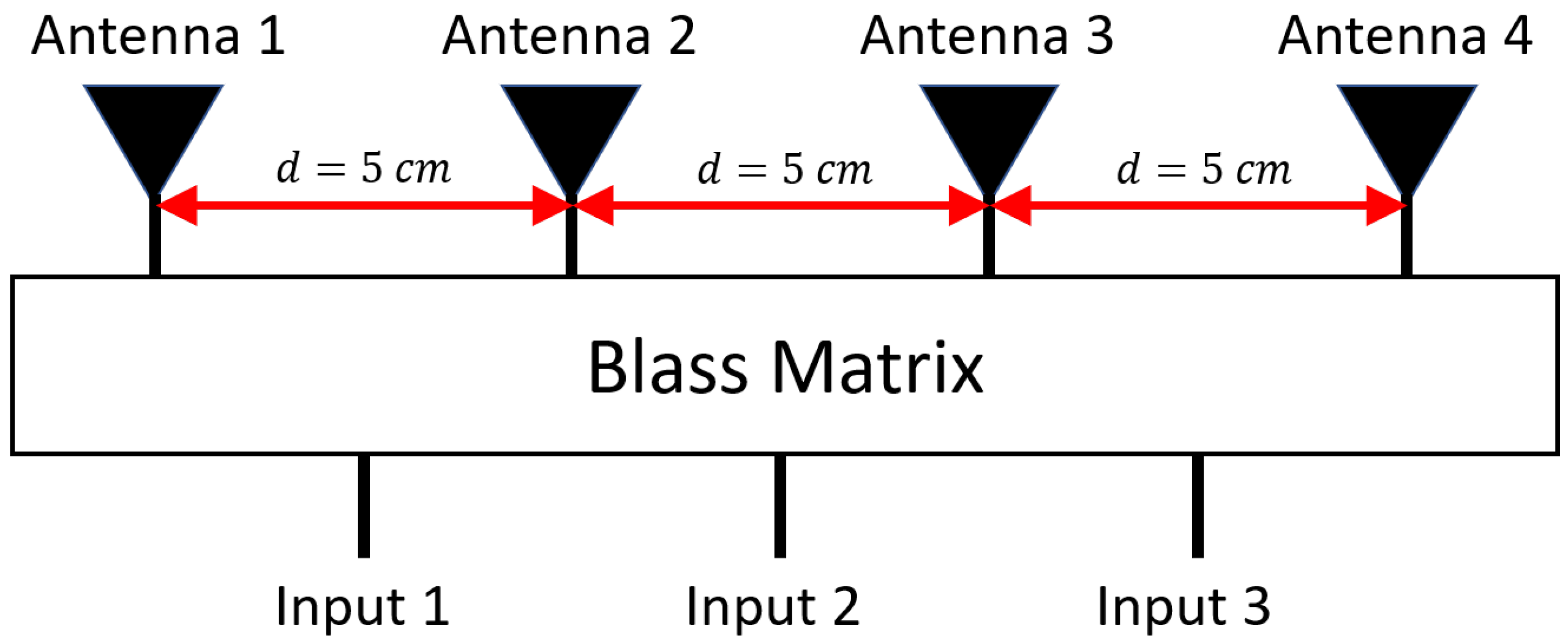
2.1. Blass Matrix Architecture

In this task, we pursue the development of a novel dual-layer Blass matrix. Typical Blass matrices are large in size and suffer from excessive losses. Aiming to compact and highly efficient mm-Wave beamforming networks in this work, the classical Blass matrix topology is first transformed into a circular design, and then implemented in a two-layer topology. To our knowledge, this is the first multi-layer Blass design. Compared to the typical single-layer Blass matrix, the proposed dual-layer network achieves 60 % size reduction. An additional key point of our implementation are the couplers. Typical approaches use bondwires and bridges [48], two factors that decrease the efficiency of the beamformer and increase the design complexity in regular Blass matrices. Here, to minimize the losses and significantly reduce the design complexity, a dual-layer directional coupler is designed and used.
The Blass matrix was first introduced in 1960 [28], and its network is shown in Figure 3. In its original form, the Blass matrix consists of N traveling wave feed lines (rows) cross-connected to a set of M transmission lines (columns), each one feeding an antenna element of the array. M and N are independent and they can be chosen arbitrarily, but always the number of beams M should be less (or equal) to the number of antenna elements. The other end of the line is terminated in a matched load (see Figure 3). This beamforming network provides M beams with an array of N elements. The interconnections are implemented with directional couplers of unequal power divisions as shown in Figure 3. For a uniform amplitude excitation of the array, the first (out of N) row of couplers divides the power to a 1 / N portion that flows towards the antenna element and a ( N 1 ) / N portion that flows along the column towards the rest of the network. Likewise, the second row of couplers divides the power into ratios of 1 / ( N 1 ) and ( N 2 ) / ( N 1 ) and so on. In addition, as long as we are moving farther away from the feeding ports and towards the radiating elements (element 1, element 2, …, element N) additional electrical length is introduced causing a true time delay (TTD) difference between the elements, which is responsible for the beam-steering of our array. By appropriately choosing the lengths of these paths, we can steer the beam at the desired direction. However, as long as we are moving towards higher port number (port 1, port 2, …, port M), the signal may travel to a specific radiating element along different paths (Figure 3). Take for example port 2 when it excites the radiating element 2. As shown in Figure 3, the desired signal is the one that can follow the path denoted with green line. However, there is also an additional path that the signal can take, which is the one denoted with red line. This second path is undesired and is referred to as spurious path, which is responsible for some performance degradation of the Blass matrix.
Aiming to a compact mm-Wave beamforming network, a dual-layer semi-circular Blass matrix adopted herein is introduced [47]. Figure 4 shows a graphical representation of the circular topology. The semi-circular Blass matrix is designed so that beams 2 and 3 are identical to beam 1, but smartly rotated so that the transmission line between them introduces the desired time delays. Therefore, for the first beam, the time delay for the nth element is n τ v e r t i c a l , for the second beam is n ( τ v e r t i c a l + τ h o r i z o n t a l ) , while for the third beam is n ( τ v e r t i c a l + 2 τ h o r i z o n t a l ) . By determining τ v e r t i c a l and τ h o r i z o n t a l , each beam can be accurately steered in the desired direction.
A critical component of the Blass matrix is, as expected, the coupler. The couplers used in this work are directional, but, unlike traditional couplers [48], they have their through port on the opposite side of the coupled port. Traditional couplers can exhibit this behavior by using either bondwires and bridges, such as the Lange directional coupler (see Figure 5b) or branch-line directional couplers (see Figure 5a). However, the first approach increases significantly the losses as well as the fabrication complexity especially at mm-Wave frequencies, while the second approach leads into a significantly larger design. To avoid both the bondwires’ complexity and minimize the undesired losses, a dual layer directional coupler is used [49], as shown in Figure 6. This coupler is comprised of two rectangular patches (Figure 6) printed on the top and bottom surface of a two-sided substrate with a common ground plane. The two patches are coupled through a rectangular slot etched on the common ground plane. The dimensions of the patches and the slot are selected to achieve the desired coupling coefficient. To design the coupler, a quasi-static approach is initially used, utilizing the design formulas given by Wong [50]. Then, the design is optimized by running full-wave simulations.
As mentioned above, one of the most critical components of the Blass topology are the directional couplers. Let us take the case when all couplers have the same coupling coefficient as proposed in [28]. In this case, the higher are the coupling values (see Figure 3), the higher is the circuit efficiency we can achieve. This is expected as more power will be distributed to the radiating elements, instead of getting dissipated at the lines’ terminations. Moreover, it can be easily observed that, for every non-spurious path case, the input signal realizes only one coupling value (see in Figure 3 how the signal flows from input port 2 to output port 2) before it reaches any output port. Therefore, an effect of the order of C [e.g., O ( C ) ] is introduced on this signal, both in amplitude and phase. On the other hand, for the case of a spurious path, the signal has to travel through at least three “coupled ports”, introducing an effect of at least O ( C 3 ) . Thus, the lower the coupling coefficient of the coupler is, the lower the effect of the spurious path is. Therefore, there is a trade-off between the efficiency of the network and the errors introduced on both the amplitude and phase of the excitations. For our case, we choose as a good balance coupling values of C = 11.5 dB [see Figure 7a]. In the next subsection, the design methodology of the proposed N × M Blass matrix beamforming network is presented.

Blass Matrix Design Methodology

As mentioned above, a Blass matrix consists of M traveling wave feed lines (columns) cross-connected to a set of N transmission lines (rows), each one feeding an antenna element of the array. The first step of the design process is to choose the number of inputs M and outputs N, respectively (in this work, M = 3 and N = 4 ). Aiming to steer the beams of our antenna array in a specific direction, the desired phase differences Δ ϕ ( n + 1 , n ) ( m ) between the output ports for each m beam are computed, utilizing array theory [51]. Recall that, for a linear phased array with interelement distance d, phase difference Δ ϕ , or group delay τ , to steer the beam toward an angle θ 0 from broadside is (e.g., [51]):
Δ ϕ = ω d sin θ 0 c o r τ = d sin θ 0 c
where c is the speed of light in vacuum and ω is the angular frequency. Although a true-time-delay beamformer is sought, its design is based on the corresponding phase differences. These are first estimated at the center frequency based on standard antenna array synthesis. In turn, phase differences are transformed to the corresponding group delays to implement the desired wideband true-time-delay antenna array. Note that, since we are proposing a Blass matrix implemented in a semi-circular dual-layer topology, which to our knowledge has never been reported before, significant modifications have to be done on the design approach compared to the classical Blass matrix [28]. Namely, the directional couplers as well as the feed-lines’ lengths between the couplers have to be appropriately chosen and designed.
The Blass matrix design methodology is a serial process, which is performed column-wise. Namely, we start with the design of column 1 adding the appropriate couplers and lengths of lines at each row 1 M , respectively. A dual-layer directional coupler in Figure 6 is used herein to accommodate our novel implementation. Since this Blass matrix has N = 4 output ports, four directional couplers are needed at each column. Between the couplers, a transmission line with a group delay τ v is added. The purpose of this line is to introduce some physical separation between the couplers for fabrication purposes and is usually chosen to be around 8.3 p s at the frequency band we have chosen to operate. In addition, the couplers have to be symmetric and form a “cross”, as shown in the schematic of Figure 3. To achieve this geometrical configuration, the top and bottom patches of the coupler are tilted at 45 ° , while in addition 45 ° arcs are introduced at the ends of the patches, as shown in Figure 6. Note that the radius of the arcs has to be chosen wisely as firstly the characteristic impedance of the corresponding lines have to remain unaffected, and secondly the coupler has to remain compact. The length as well as the width of the slot and the patch are designed following the methodology in [49,50]. The total phase difference between the coupler’s input-port and its through-port is denoted as Δ ϕ c and the corresponding delay τ c . In addition, the coupling value is decided by the patch and slot width, and are always 90 ° in terms of electrical length. Thus, the phase introduced due to the coupling value is negligible. Therefore by looking at the Blass matrix schematic (see Figure 8) the total phase introduced at the nth output-port, when input port m = 1 is used as a reference, is:
Δ ϕ n , 1 ( 1 ) = n Δ ϕ c ( N n ) Δ ϕ 0 τ n , 1 ( 1 ) = n τ c ( N n ) τ 0
where Δ ϕ 0 is the phase introduced by line τ 0 . From Equation (2), it can be seen that the phase difference between two adjacent output-ports ( n , n + 1 ) is:
Δ ϕ n + 1 , n ( 1 ) = Δ ϕ c Δ ϕ 0 τ n + 1 , n ( 1 ) = τ c τ 0 = τ
Using Equation (3), the electrical length of line τ 0 can be specified. Since τ is the desired group delay estimated from the antenna array in order for the beam maximum to point toward the pre-specified direction θ 0 , it can similarly be seen that for column 2 the phase differences between adjacent output ports are:
Δ ϕ n + 1 , n ( 2 ) = Δ ϕ c Δ ϕ 0 Δ ϕ h τ n + 1 , n ( 2 ) = τ c τ 0 τ h
where Δ ϕ h is the phase introduced by line τ h . In a similar manner, the rest of the matrix columns are designed. The last step of the design methodology is to choose the coupling coefficient of the couplers. As mentioned above, all beams except from the first one suffer from spurious excitations. These excitations degrade the performance of the Blass matrix by introducing perturbations in amplitude and phase, as shown in [28] (Equation (6)). It can be seen that the higher the coupling value is, the stronger the effect of these perturbations is, ultimately degrading SLL. On the other hand, if a low coupling value is chosen, only a small portion of the power will be coupled to the output ports, and the rest will be consumed by the terminations (see Figure 3). Therefore, the coupling value is determined by the application and how tolerant this application is to high SLL values.

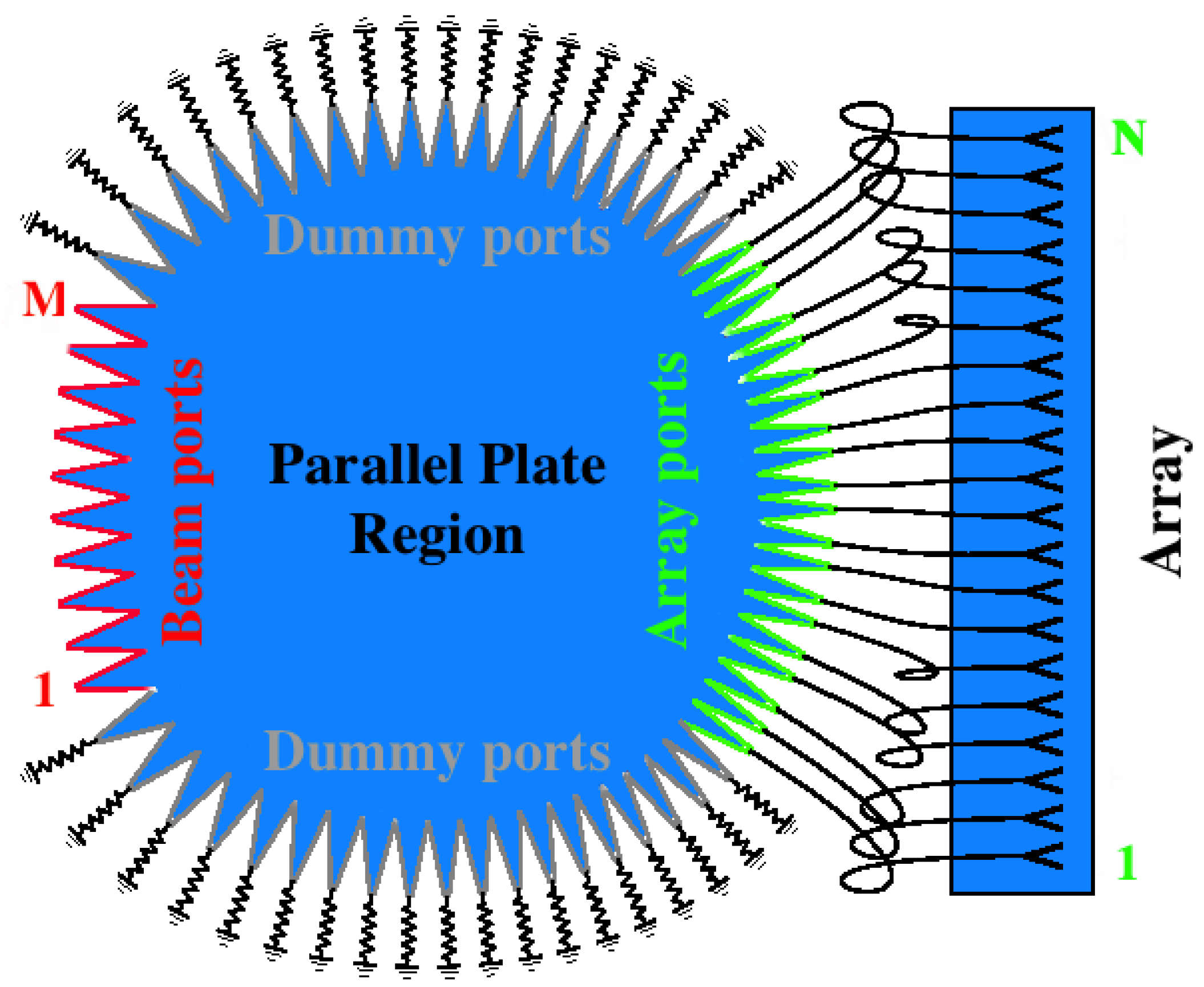
2.2. Rotman Lens Architecture

In our second approach, a novel true time delay Rotman lens is used. Rotman lenses, similar to classical Blass topologies, are known for two main limitations: their large footprint and their limited efficiencies (typically 50–60%) due to the dummy ports. Aiming at high efficiency, we propose a novel dummy-ports-free Rotman lens utilizing the idea of field absorbers. Specifically, imitating perfect matching layers (PMLs), we engineer the substrate by doping it with conductive material. This key modification essentially increases the loss tangent about ten times, yielding an almost perfect absorber and eliminating the undesired reflections.
As is well known, the original Rotman lens is a metallic plate waveguide, loaded with dielectric for miniaturization purposes, where its input ports lie upon the beam contour and the output ports lie upon the array contour. As its grounded substrate is extended beyond the waveguide boundaries for practical purposes, it resembles a printed microstrip structure, although the area between the two metallic planes remains a parallel plate waveguide operating at its TEM mode.
As shown in Figure 9, the Rotman lens is considered as a M × N beamforming network. Its functionality is: when an input port is excited, the input signal is divided into N output ports with different amplitudes and phase sequences, which create a radiated beam with its maximum directed along a specific direction. When the same input signal is fed to another input port, a beam oriented to a different scanning angle is created. The energy fed to each input port emerges as rays directed towards all possible directions inside the parallel plate region. Some of them collimate, feeding the antennas through the output ports. However, there are also rays that propagate towards the top and bottom sides of the waveguide (in Figure 9, the top and bottom sides are considered the sides where the dummy ports are placed). These rays may be reflected to arrive at the output ports (even at the input ports) interfering with the directed rays at arbitrary phase, thus "contaminating" the desired signals (or causing mismatching at the inputs). Hence, the energy of these side-propagating rays must be absorbed and dissipated when they arrive at the side edges of the lens. To reduce the reflections in the parallel plate region, the dummy ports are used, as shown in Figure 9. Essentially, the dummy ports serve as absorbers for the spillovers of the lens, reducing the multiple reflections and standing waves, which undermine the lens performance [52].

Rotman Lens Design Methodology

In this work we follow the classical Rotman lens design approach, as depicted in Figure 10 given by [52].
Aiming at a compact, low cost, and highly efficient design, our goal is to minimize the number of dummy ports. However, when a small number of dummy ports is used, the Rotman lens performance degrades radically, as the inputs are no longer well matched, and the outputs’ phase response fluctuates leading to a non-constant group delay. This is a well-recognized problem and numerous attempts have been made by researchers to confront it. Indicatively, Sorrentino et al. [53] utilized field absorbers at the side edges built up on a metamaterial approach. Here, we take a different path, imitating the perfect matching layers (PML). For this purpose, we appropriately engineer the substrate by doping it with conductive material, (e.g., carbon), on the area directly beyond the sides of the upper metal. This is considered to retain about the same dielectric constant but increasing the loss tangent about ten times. Thus, we can efficiently absorb the incident waves and in turn attenuate the standing waves of the parallel plate region. Following the principles of electromagnetic theory, the attenuation constant for the case of a TEM propagating mode in the parallel plate region when material losses are introduced is given by [48]:
a d = k t a n δ 2
where k = ω ϵ μ stands for the wavenumber. Considering the desired frequency of operation and keeping in mind that the mode attenuates at a rate of e a d x in the parallel plate region, we can evaluate the distance the wave has to cover to attenuate 1 / e in respect to its initial value. Based on this initial estimation the Rotman lens’ absorbing area is initially designed and then in turn is optimized using an EM simulator. In our proposed design, following this procedure and after the necessary optimization, the length of the structure increases almost 6 % with respect to the dummy-ports-based design, ensuring sufficient absorption of the incident waves in the side walls. Figure 11 presents how the dummy-port based design has been modified when absorbers are introduced in the side walls.
This approach is proven to yield an almost perfect absorber, eliminating reflections along with their deleterious effects on the input matching and output phase fluctuations. The challenge here is to invent practical ways for the implementation of the assumed “conductive doping”. A simple structure with only three input and three output ports is considered herein as a proof of concept, and it is proven to work very well.

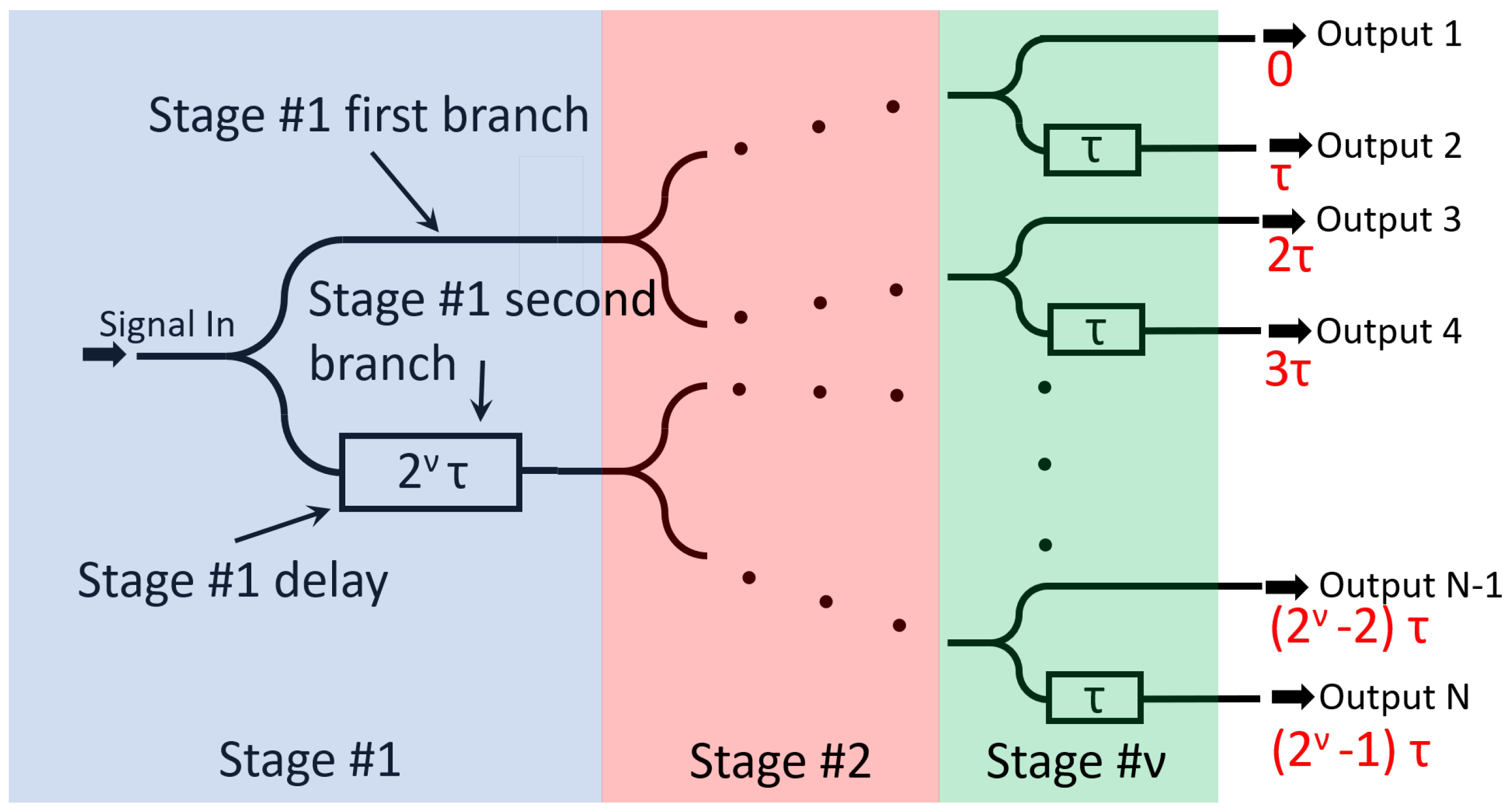
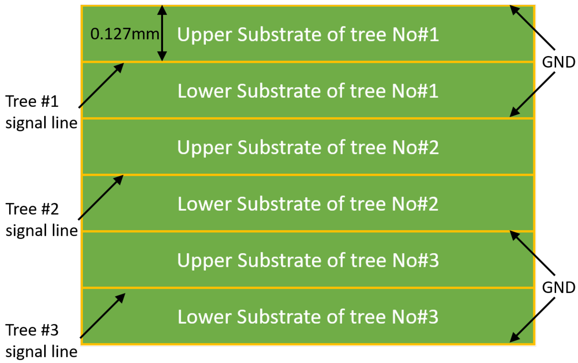
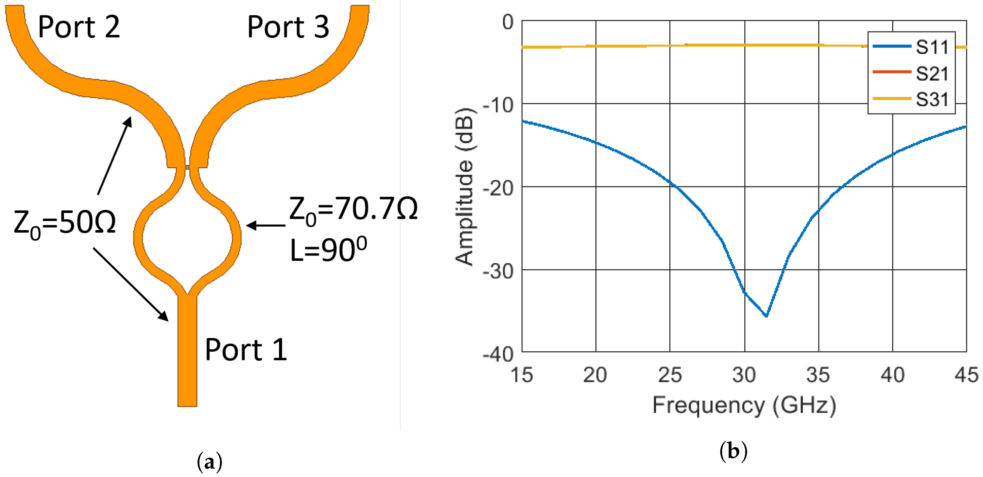
2.3. Tree Type Beamforming Network Architecture

Our last design is focused on the development of a novel tree-based beamforming network, which mimics topologies that have been employed in microwave photonics [54]. We expect that this design will enable the development of new tunable three-dimensional (3D) beamformers for next-generation hybrid phased array systems providing game-changing capabilities compared to other beamformers. Specifically, the proposed implementation provides ultra-wideband operation, eliminates the problems of crossovers faced by Butler, Nolen, and Blass matrices, and is capable of exhibiting significantly higher efficiencies than Rotman lenses. Figure 12 shows our proposed tree topology. As can be seen, the building blocks of this topology are transmission lines and power dividers, making its topology relatively simple. The primary novelty of this topology is the minimal number of the involved delay lines. This idea stems from microwave photonics, and it is exploited in microwave and millimeter wave regimes. The key feature to observe refers to the hierarchical usage of delay lines with multiples of the basic delay τ from the antenna ports level towards the transceiver port. The idea is to hierarchically repeat the same feature by doubling the delay while moving diagonally from the first antenna port towards its last port and towards the network input. Specifically, the signal entering the input port undergoes successive power divisions by reaching the output ports with both the desired amplitude and phase. Even though our proposed design looks similar to corporate-type beamforming networks [55], the time delays in the form of transmission line paths are introduced in the common branches and not before the output ports of the network. This modification is crucial as it offers two main advantages. First, in the tree topology, the total delay (or phase shift) is introduced through the common branch, instead of the multiple small branches used in the corporate network that introduce the desired time delays in parallel. This key modification makes the tree beamforming network significantly more compact compared to the corporate network. Secondly, and most importantly, the transmission lines playing the role of phase shifters are true time delay elements, which eliminates the beam squint phenomenon. As is expected, a tree-based network can introduce only a specific time delay, steering the beam towards only one specific angle. However, this limitation can be overcome using multi-layer topologies with a different tree network on each layer, where each layer is devoted to steer the beam towards a specific angle. Figure 13 shows in detail our proposed multilayer design. To connect the different layers a single pole multiple throw (SPNT) type switch is used at the input and at each antenna port to effectively activate the corresponding layer (tree-topology) and provide the desired radiated beam (thereby achieving beamsteering). The challenge here is to appropriately design the interconnecting lines so that they are compatible with the monolithic microwave integrated circuits (MMICs) of SPNT switches. To address this challenge, all the interconnecting lines are designed as striplines, an approach that has never been implemented before on these networks. This design approach not only provides the needed multilayer beamformers but also ensures low losses at mm-wave frequencies.
As is expected, a critical component of the tree beamformer is the power divider. The power divider has to be appropriately designed to support the required bandwidth while it simultaneously introduces the desired amplitude distributions at the radiating elements of the network. At this stage of our research, we are only focused on the second aim, leaving the wideband behavior as a future task. Our goal is to design a beamforming network that can introduce Chebyshev distribution at the antenna ports. To achieve the Chebyshev distribution, asymmetric power dividers have to be designed by appropriately distributing the power at their ports and throughout the network. Conventional unequal power division Wilkinson power dividers can achieve the unequal power split by introducing an asymmetry in the characteristic impedance of their two branches. This way excellent performance is achieved in relatively small power division ratios. As the power division ratio increases, however, the characteristic impedances of the branches acquire very large or very small values, which are unrealizable in microstrip or stripline technology. Large characteristic impedance lines tend to be very thin and sometimes outside of the manufacturing tolerances, while small characteristic impedance lines are very wide, introducing large parasitic capacitances, thereby making them inappropriate for our application. Therefore, unequal power division Wilkinson power dividers are not suitable for our design due to the different power ratios that we need to achieve. Specifically, Figure 14 shows the power divider used in this work. This unequal power divider is based on the design introduced in [56], which is capable of utilizing 50 Ω lines and introducing the desired asymmetry in the electrical length of its corresponding transmission lines. In our case, a 21 dB SLL Chebyshev amplitude distribution is excited among the elements. Therefore, the ratio of power arriving at the elements located at the edge of the array over the ones in the middle is 5.15 dB.

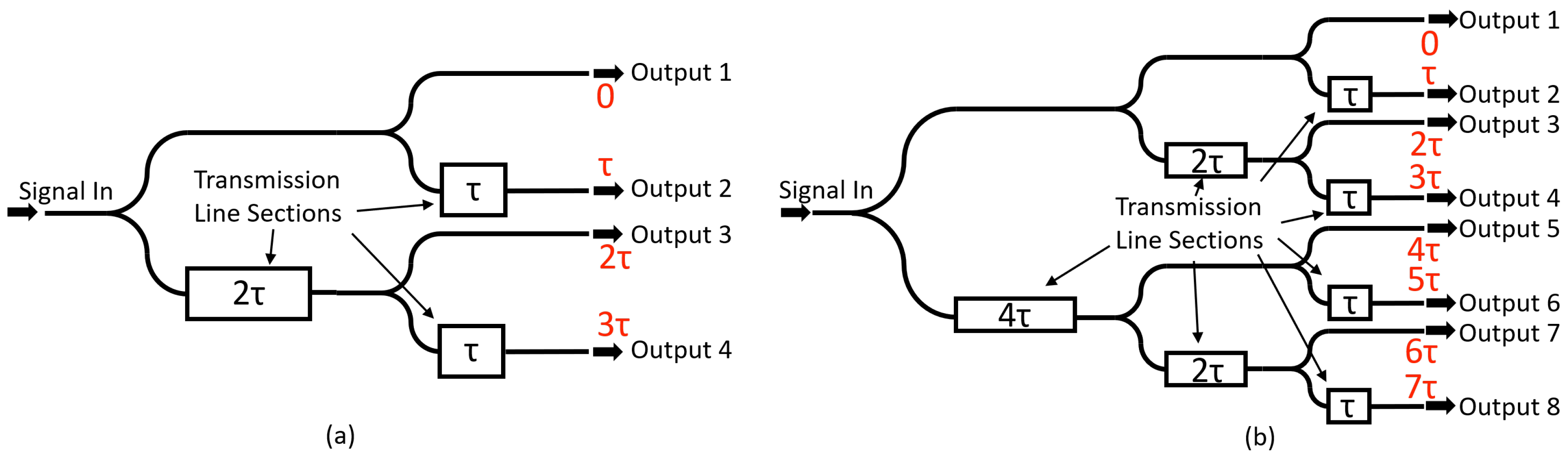
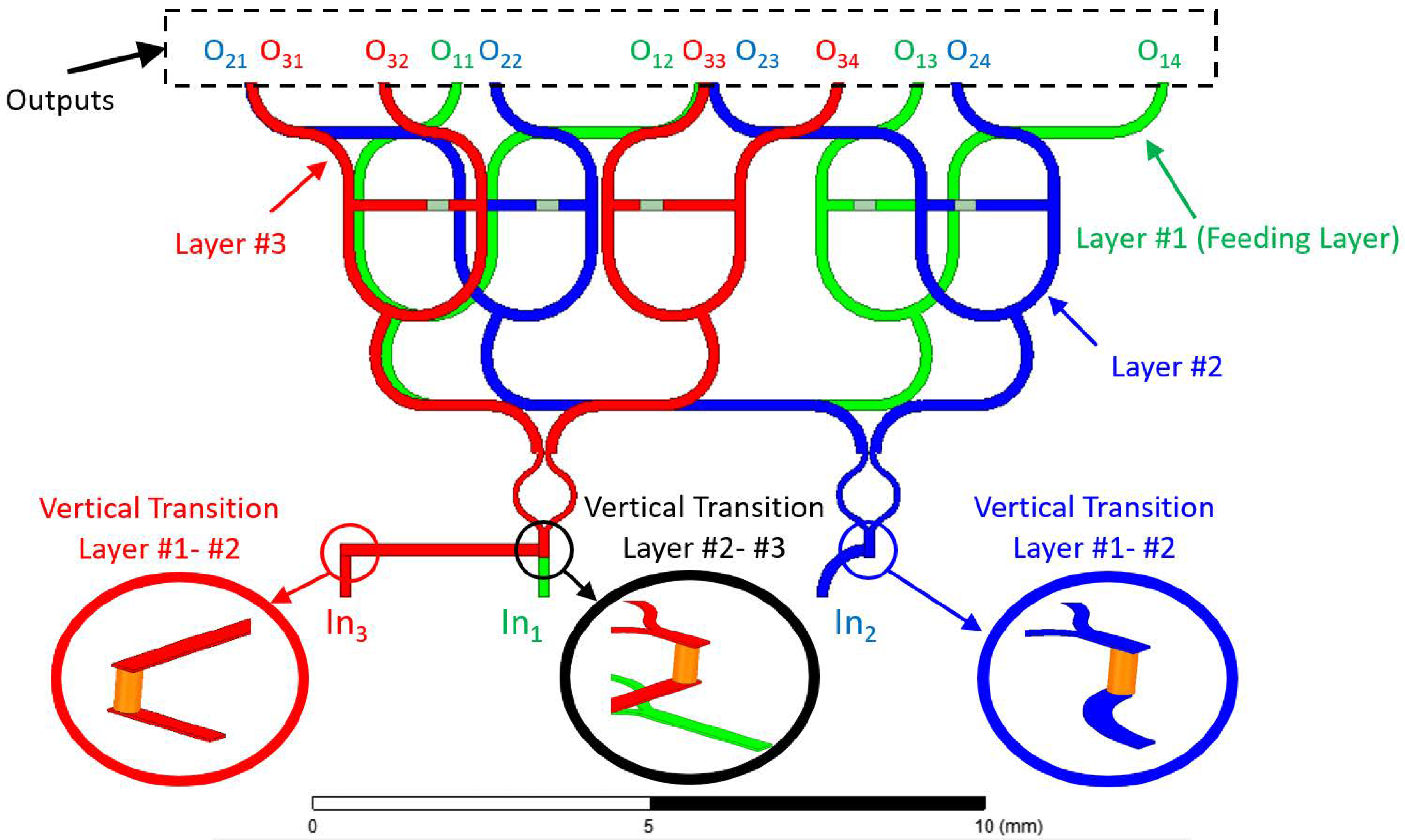
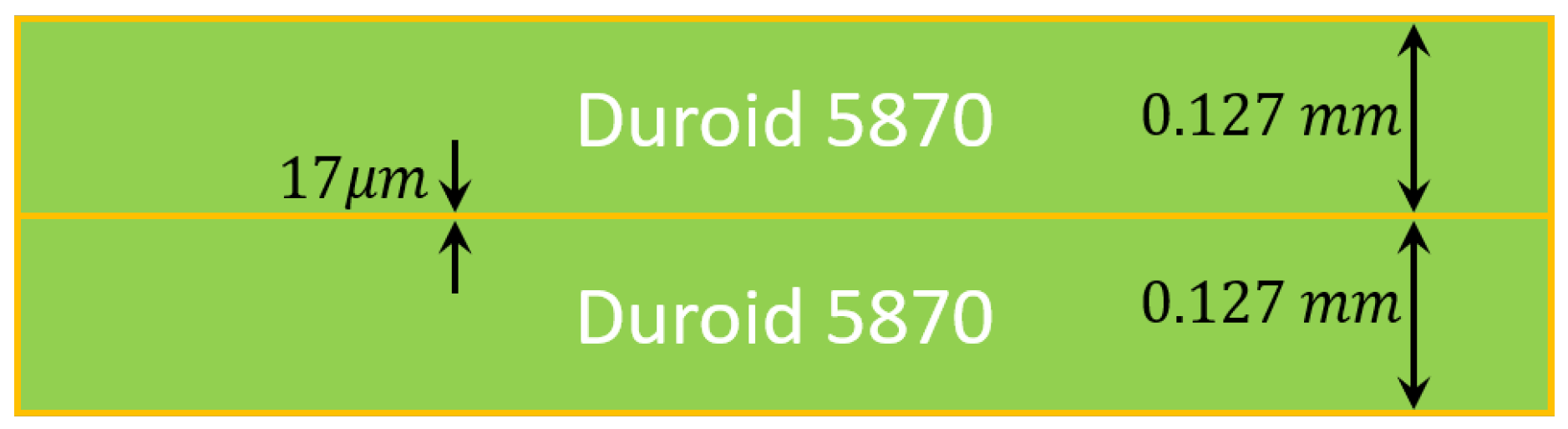
Tree Topology Design Methodology

A tree beamforming network is comprised of delay lines and power dividers. Similar to any other beamforming network design methodology, we first start by defining the number of desired output elements N and beams M. Since the tree network is capable of introducing only a specific time delay, steering the beam towards only one specific angle, for each beam direction m [ 1 , M ] , a different tree network has to be designed. In our proposed design, as we are implementing a multi-layer topology, each beam is produced by a different layer of our network. N by default can only be a power of two N = 2 ν , with ν denoting the number of stages used to implement the tree network. Figure 15 shows one layer of a general schematic for the tree type network implemented with ν stages and N outputs.
Aiming to steer the beam at a specific angle, the phase difference Δ ϕ between the adjacent output-ports, corresponding to a frequency independent delay of τ as in Equation (1). Thus, a Δ ϕ = ω 0 τ at the center frequency ω 0 , is chosen, following the array theory [51]. In addition, as the tree topology offers us the ability to apply any tapering distribution we desire, the appropriate amplitude coefficients at the output ports are chosen. Herein, a Chebyshev array with a predefined S L L = 21 dB is employed. These are achieved by appropriately choosing the power division through the network’s cascaded power dividers. The whole design philosophy is deployed as we move from stage 1 (left) to stage ν (right), as depicted with different colors in Figure 15. Assuming that P n is the power arriving at each output port, the first stage power divider (in Figure 15, it is denoted with purple color) is designed to have a power division ratio of:
C 1 = i = 1 N / 2 P i i = N / 2 + 1 N P i
Note that, when the amplitude tapering is symmetric, this ratio is equal to one. In addition, the electrical length of the first stage delay line is Δ ϕ 1 = ( N / 2 ) Δ ϕ . Moving to higher-order stages (e.g., stage 2– ν ), the power division ratios are evaluated as:
C ν j = i = ports first branch of j th divider P i i = ports second branch of j th divider P i
while the electrical lengths and the delays of the corresponding delay lines are:
Δ ϕ ν = N 2 ν Δ ϕ = ω 0 τ ν
where ω 0 is the center angular frequency. Following this design methodology, any desired amplitude distribution is feasible maintaining the beam at the desired steered angle.

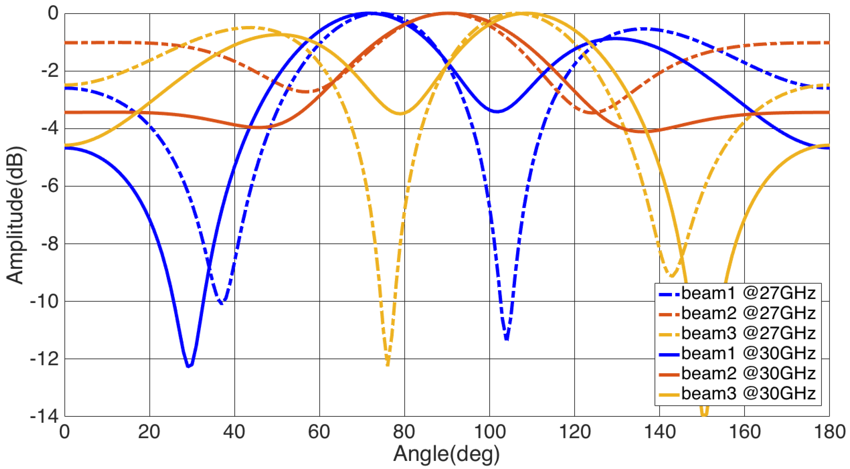
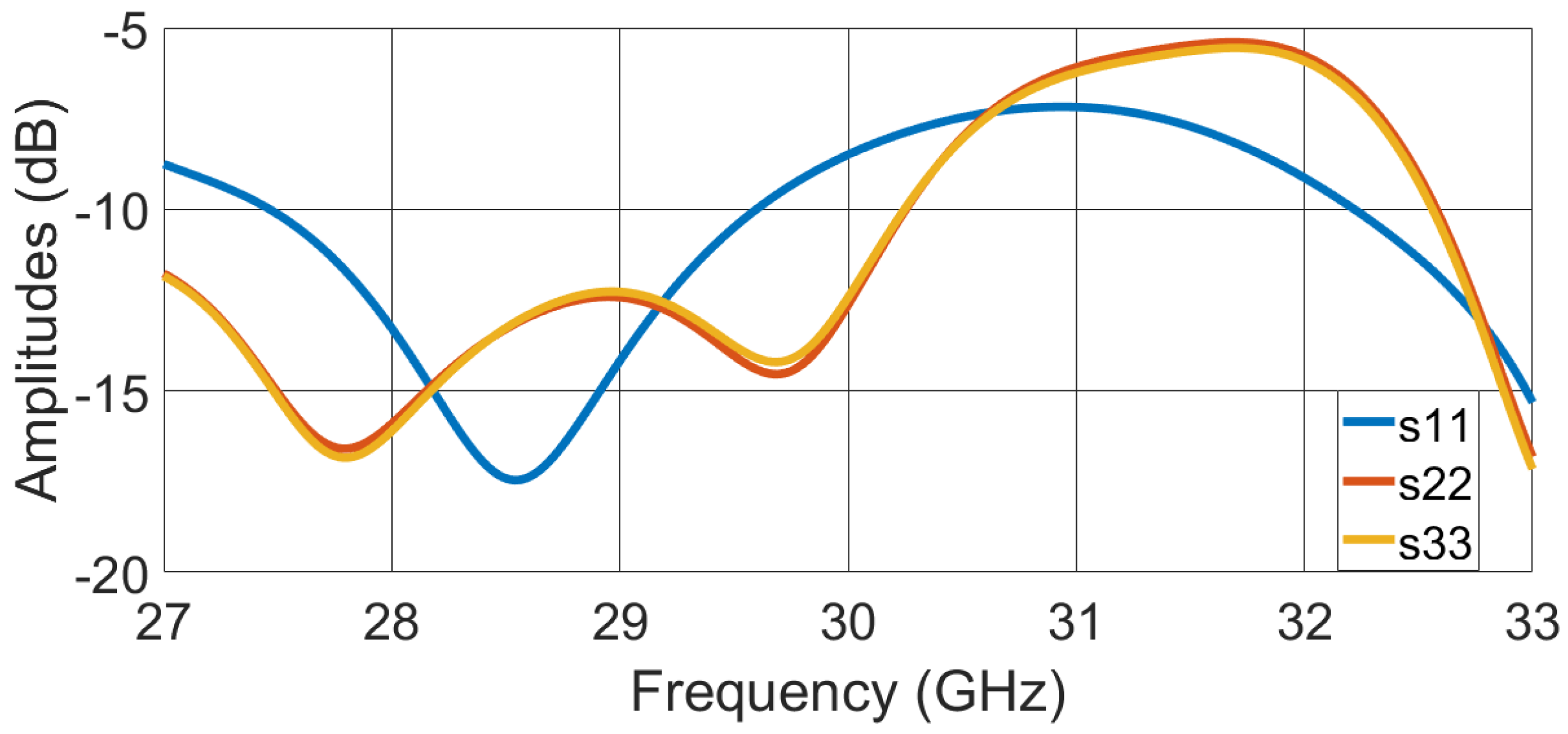
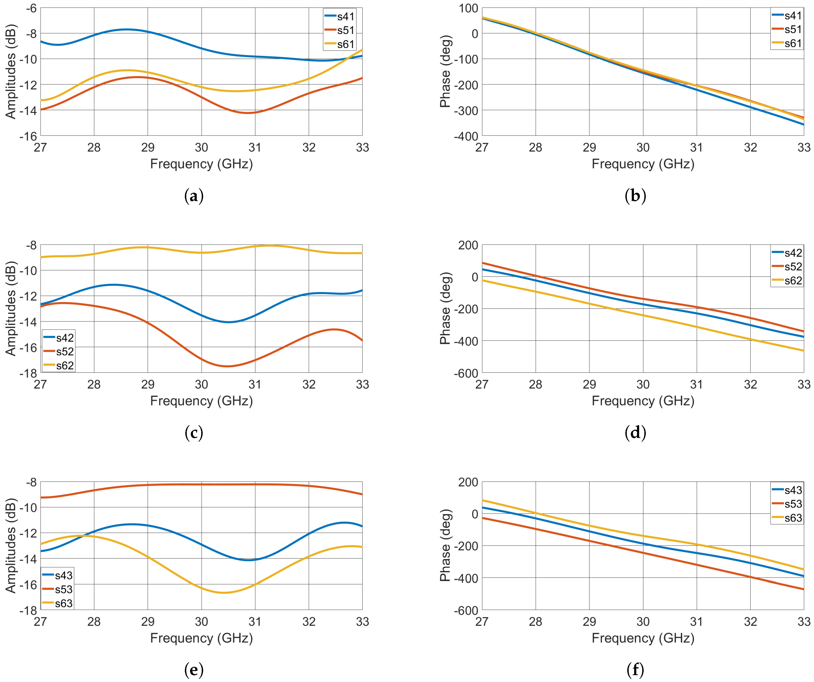
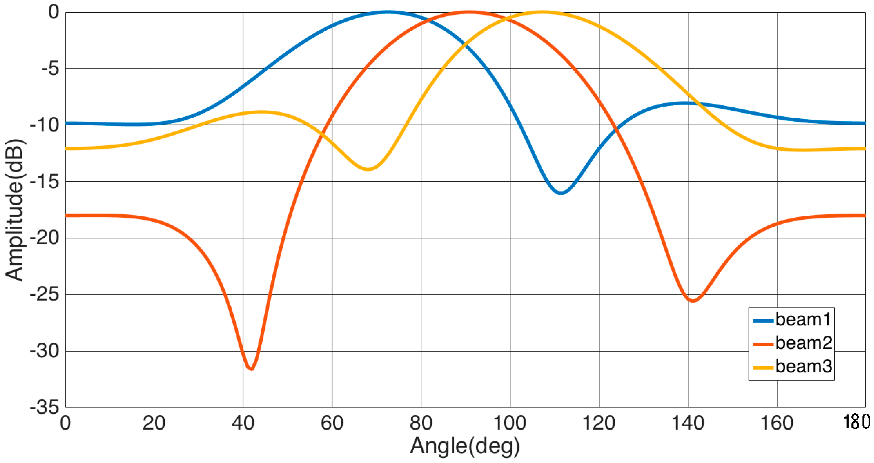
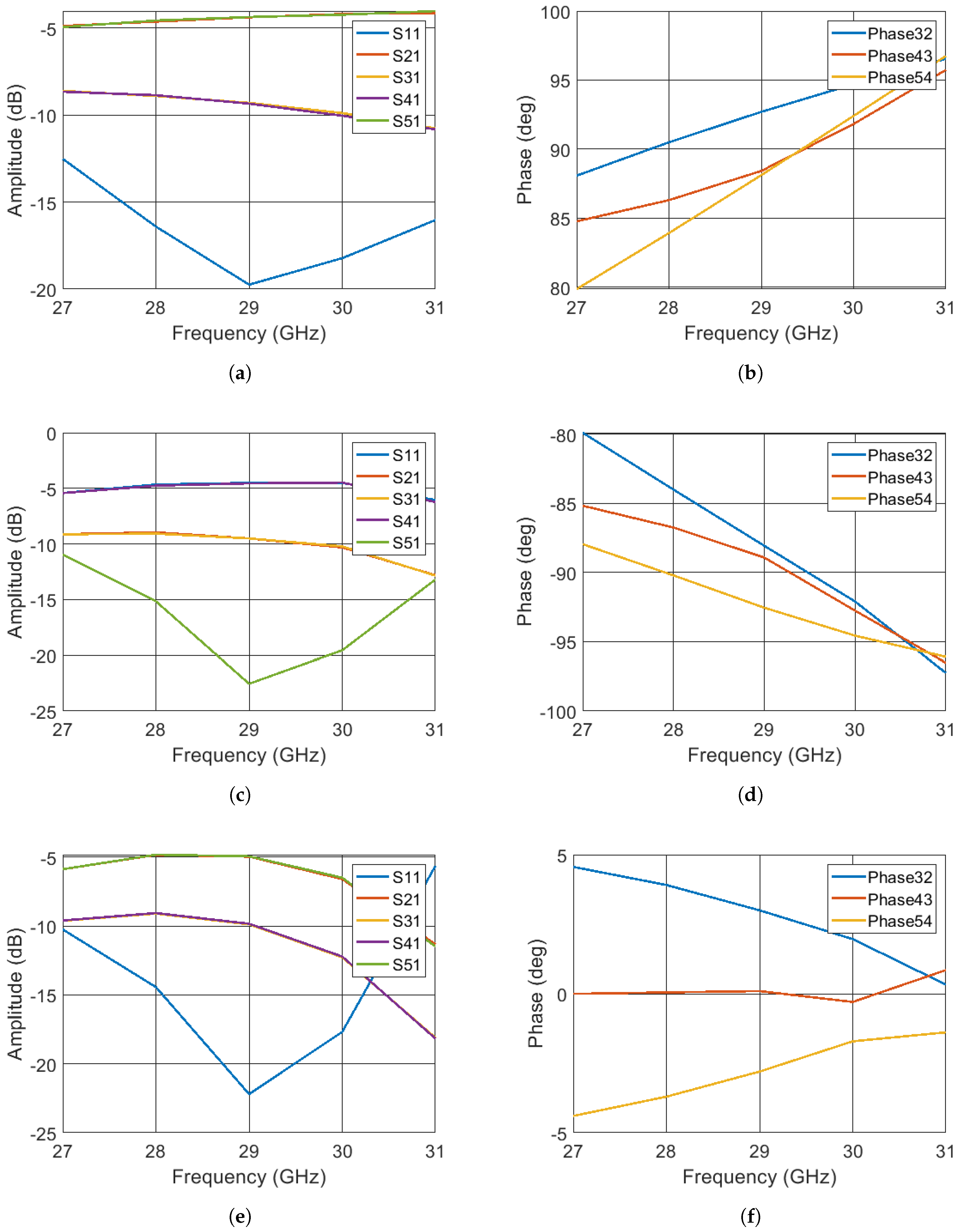
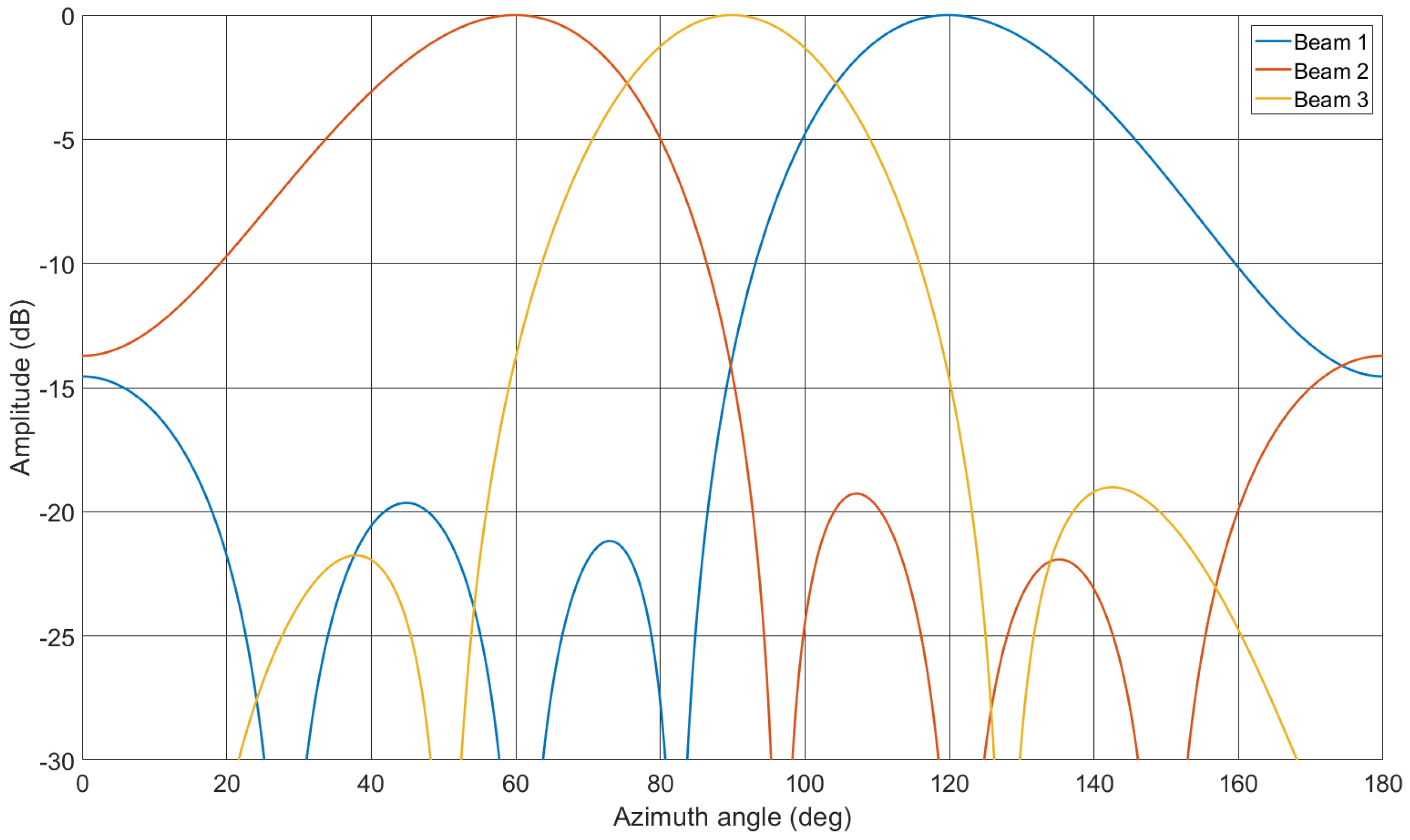
3. Numerical Results

In this section, the results of our proposed beamforming networks are organized into three corresponding subsections. Excellent performance is attained for each case network, thereby proving that they are suitable for our envisioned switched-beam phased arrays.

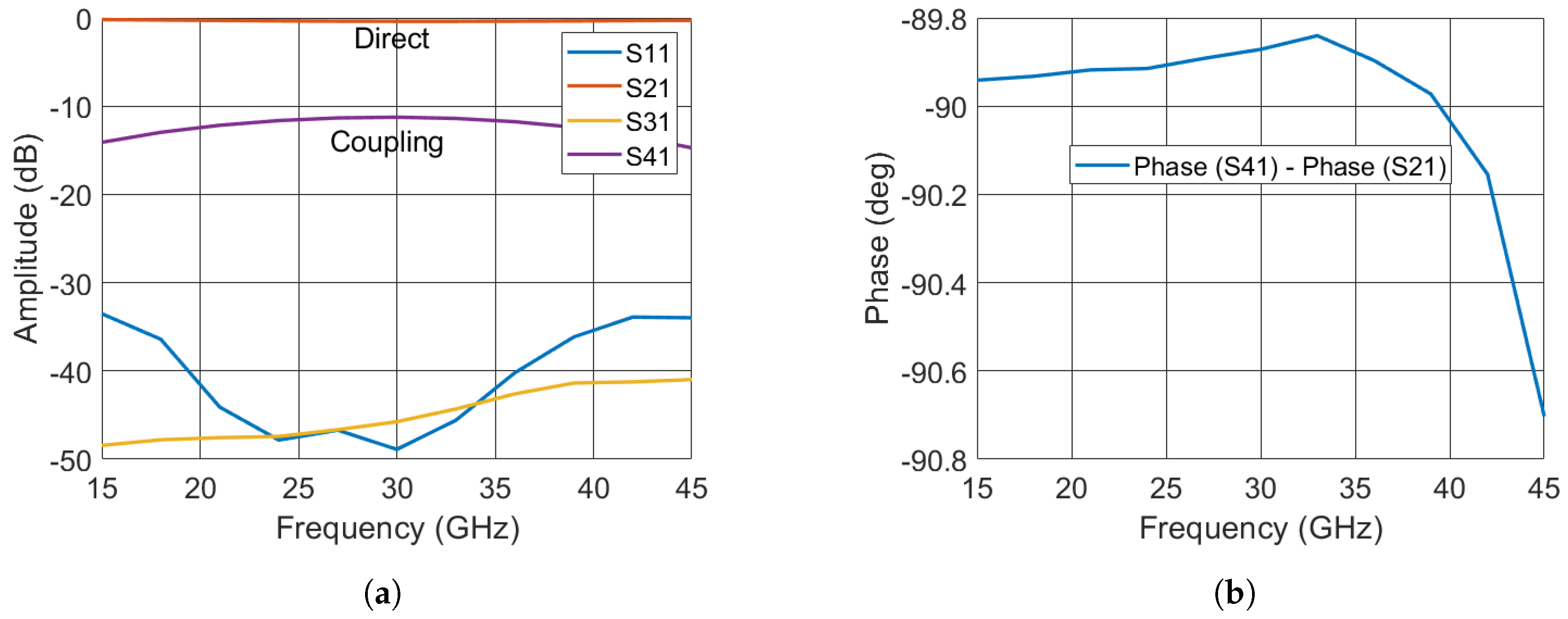
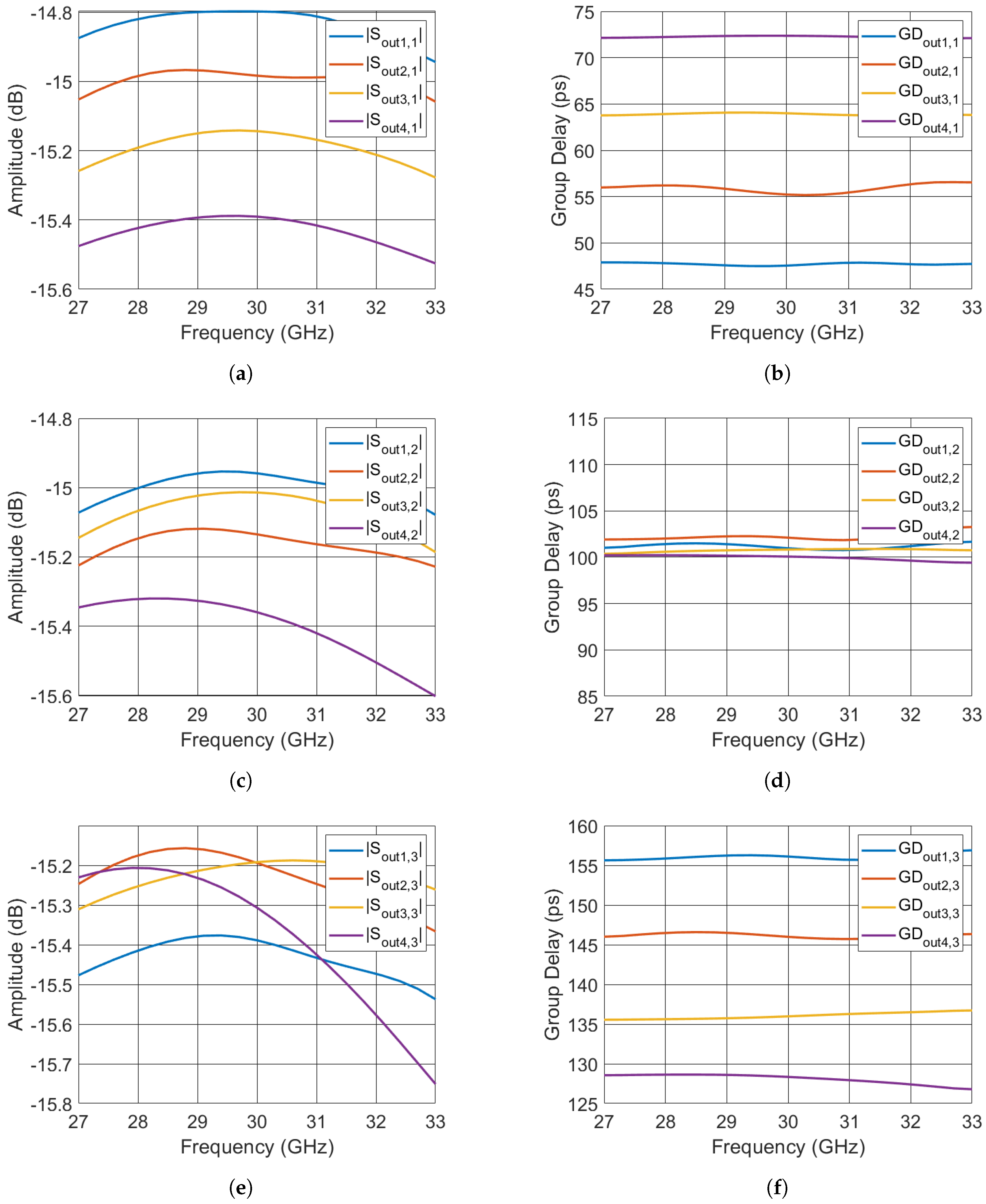
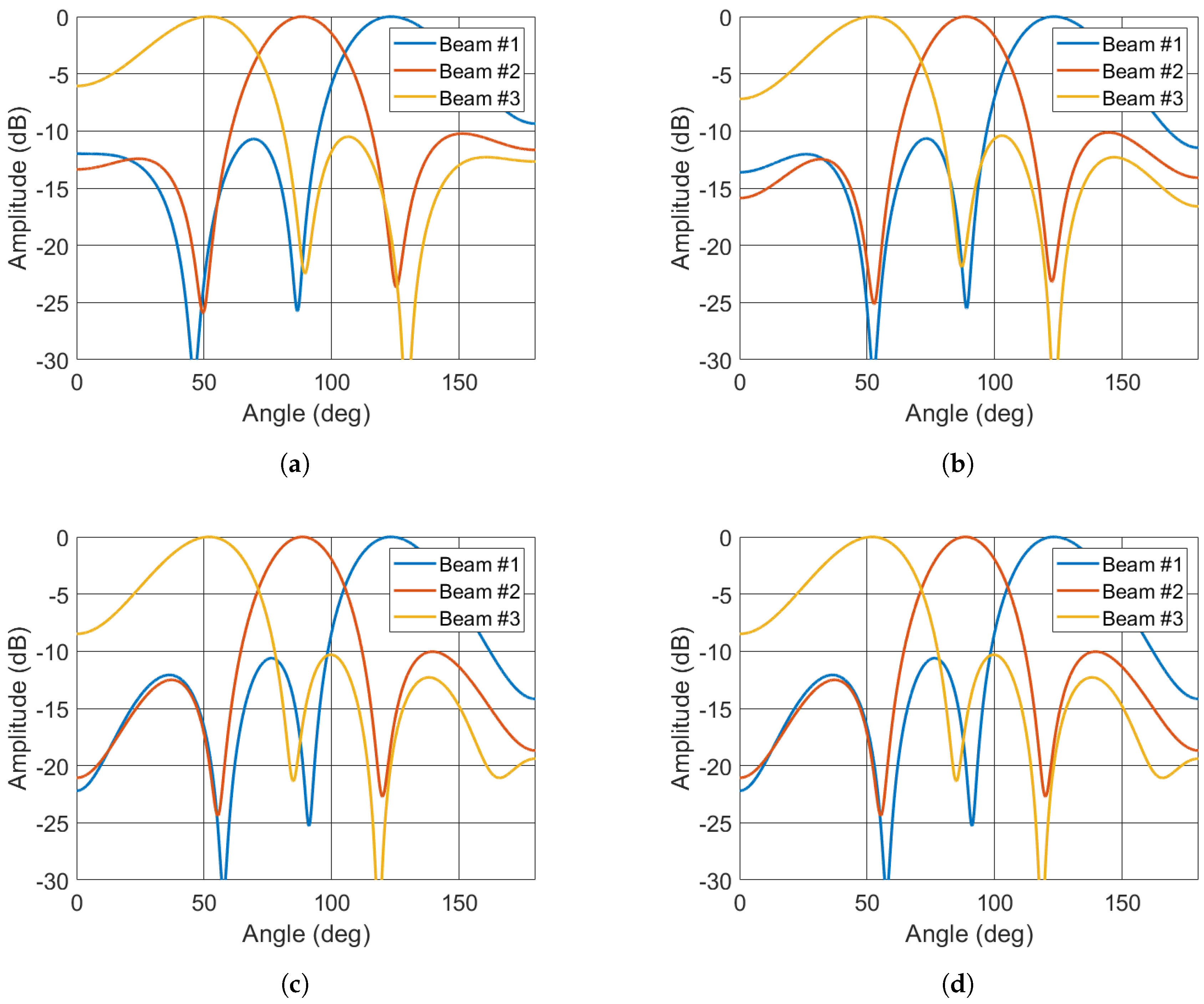
3.1. Blass Matrix Results

Figure 8 shows our proposed compact double-layer semi-circular Blass matrix that can achieve uniform amplitude distribution and steer its beam between the following three directions: broadside and ± 34 ° . Notably, the design rules of the proposed Blass architecture are based on the design equations given in the original paper by Blass [28]. The 11.5-dB dual-layer directional coupler used in our design is implemented in a double 0.127-mm-thick duroid 5870 substrate with a dielectric constant of ϵ r = 2.33 , as shown in Figure 16. The slot width is 0.4744 mm and the patch width is 0.5277 mm, which are estimated according to the methods in [49,50] to ensure an 11.5-dB coupling. The analytically estimated dimensions are 0.48 and 0.533 mm for the slot and the patch, respectively. These design parameters are optimized through the ANSYS HFSS simulation software, and the final slot and the patch lengths (see Figure 6) are 1.8 mm. Curved 50   Ω microstrip lines are attached to each side of both patches with a radius of 1.3 mm and a 45 ° arc angle. As shown in Figure 7a, the 3-dB bandwidth in terms of coupling coefficient ( S 41 ) ranges from 15 to 45 GHz, while both the return loss S 11 and isolation S 31 are satisfactory. Finally, the phase of the coupling coefficient with respect to the direct path is designed to be Δ ϕ = p h a s e ( S 41 ) p h a s e ( S 21 ) = 90 ° for all desired bands of operation, as shown in Figure 7b.
Both the second and third columns of the Blass matrix are similar to the first but rotated by 31 ° and 62 ° , respectively. The required delay lines of multiples of τ h according to Figure 4 are designed and implemented as microstrip lines, and the results are presented in Figure 17. In addition, τ 0 and its multiples are achieved through 1.987 mm straight microstrip line segments, while τ h is achieved with curved microstrip lines with a length of 2.01 mm and an arc angle of 31 ° . Multiples of τ h have the same arc angle but double the length. The vertical delay lines are chosen to have zero electrical length as, based on our simulation analysis, the coupler inserts a 18.08 p s delay on its own. Therefore, there is enough physical separation and no extra vertical lines are needed. The desired delays τ h for an array with an interelement distance d = 4.5   cm at the maximum operating frequency of f m a x = 33   GHz are illustrated in Figure 18. Notably, d = λ m i n / 2 at f m a x to avoid grating lobes. However, this could be related to higher values due to the restricted angular deflection of the radiated beam from 0 ° (broadside) to θ m a x = 34 ° degrees as d = λ 0 , m i n / ( 1 + θ m a x ) .
The simulation results of the Blass matrix topology are presented in Figure 19a–f. Specifically, Figure 19a shows that, for the first beam, which aims towards + 34 ° , the amplitudes at the corresponding elements exhibit only a ± 0.4 dB or ± 9.6 % deviation from the desired uniform amplitude distribution. As expected, the time delays of the first beam are flat for the total operational bandwidth (see Figure 19b) since spurious paths are avoided by utilizing directional couplers. As shown in the inset of Figure 19b, the time delay differences between adjacent ports are fairly constant, deviating by no more than ± 0.7 p s or ± 8.4 % . Regarding the second beam, which aims towards broadside, the amplitudes at the output ports deviate from the uniform distribution by ± 0.35 dB or ± 8.4 % , as shown in Figure 19c. Figure 19d presents the corresponding time delay of the output ports, showing a maximum difference of no more than ± 2 p s between them. Finally, for the third beam that aims towards 34 ° , which is affected the most from the spurious paths, compared to any other beam, the maximum amplitude deviation is ± 0.35 dB ± 8.4 % (see Figure 19e), and the time delay differences between the output ports differ by ± 2 p s or ± 24 % at most. It is important to note that, even though the errors seem large at a first glance, they are not systematic and they exhibit a random-like behavior. As a consequence, both the directivity and the beam pointing angle of the resulting array factors are largely unaffected. The only degradation introduced by the spurious paths can be observed at the slightly increased SLL shown in Figure 20a–d as calculated directly from the S-parameters of our network. The maximum SLL of the three beams is 10 dB and occurs for the second beam’s entire operational bandwidth. This is due to the spurious excitations, as predicted. The beam crossover level is at 4.5 dB at 33 GHz and goes up to 3 dB at 27 GHz. In summary, the operational bandwidth of the Blass design presented in this section is 27–33 GHz.

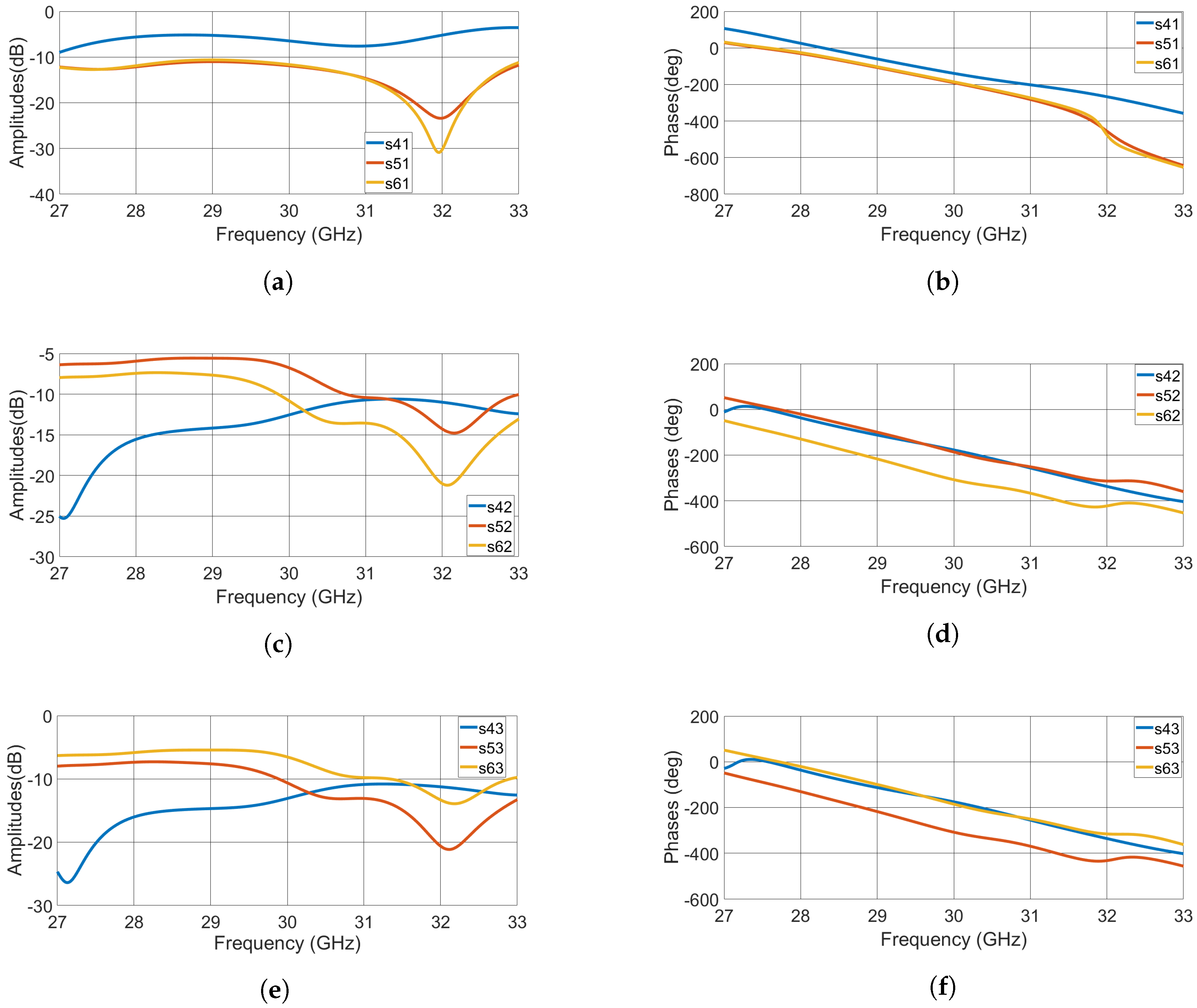
3.2. Rotman Lens Results

In this work, the classical Rotman lens architecture with dummy ports is compared with a novel design where the dummy ports are replaced by absorbers. In general, the role of dummy ports is to reduce the reflection of the incident waves at the side walls of the lens. These incident waves are responsible for the appearance of standing waves in the parallel plate region and, consequently, the degradation of lens response. By replacing the dummy ports with absorbing layers, the incident waves on the side walls are efficiently absorbed, improving the characteristics of the lens. Both designs consist of three input ports, and three output ports. Notably, the design rules of the proposed Rotman lens architectures are based on the design equations of Rotman and Turner [30]. Aiming at a compact design, a substrate Rogers RT6006 with ϵ r = 6.15 , and t a n δ = 0.0027 is chosen. All simulations were performed in the range of 27–33 GHz. The absorber material is assumed as the same substrate, but doped with conductive media (e.g., carbon) to increase its conductivity and, in turn, its loss tangent as: ϵ r = 6.15 and t a n δ = 0.7 . The presented topology serves as a proof of concept and more practical designs with higher port numbers will be investigated in the future.

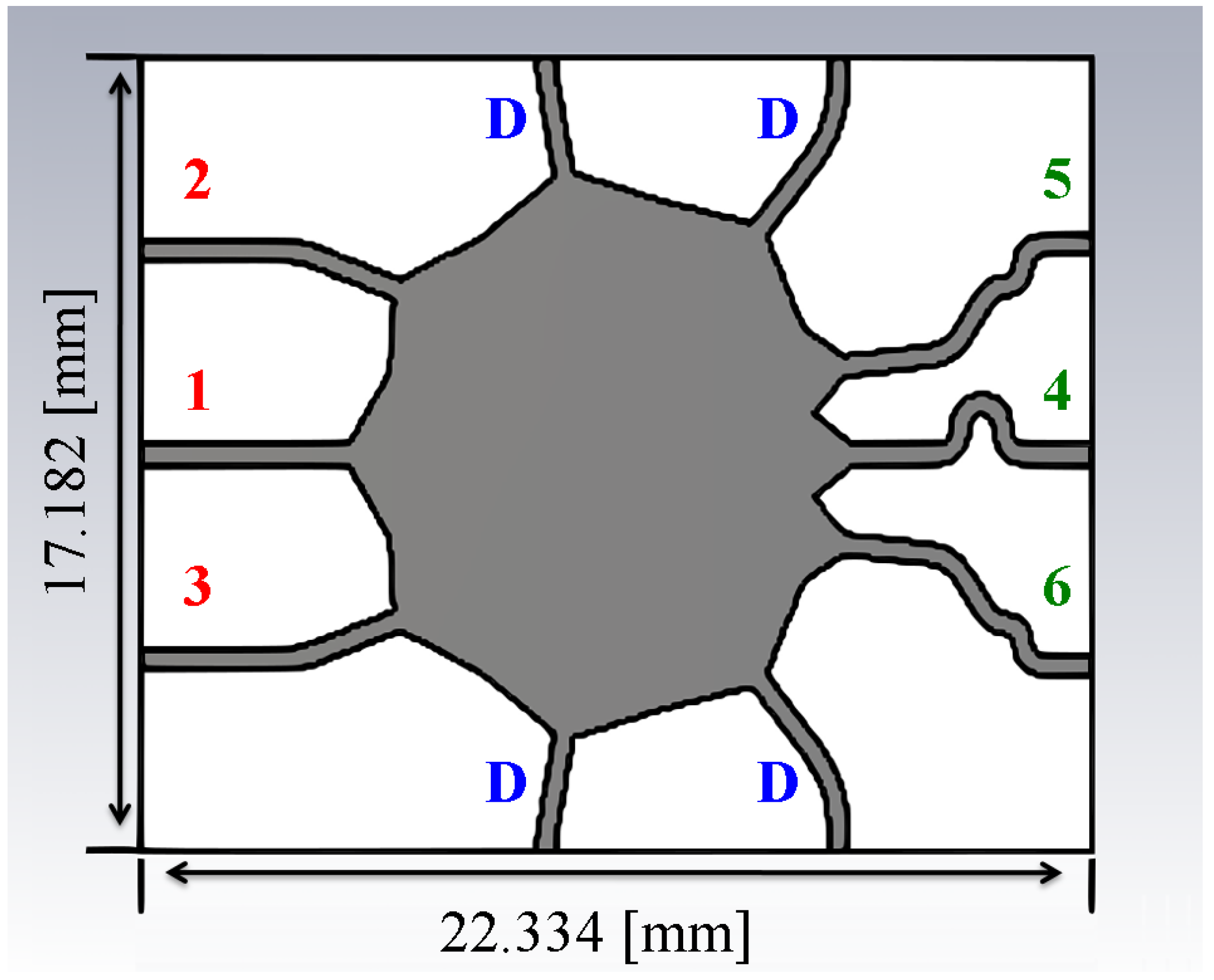
3.2.1. Rotman Lens with Four Dummy Ports

The classical Rotman lens topology studied herein consists of three input, three output, and four dummy ports, as depicted in Figure 10, with dimensions 22.334 × 17.182 × 0.3 mm 3 . The reduction of dummy ports number results in a reduced efficiency. Figure 21a–f shows the magnitude and phase distributions of the designed lens. Although the device seems to work satisfactorily in the frequency range 27–30 GHz, it has a prohibitive response in the second half of spectrum that ranges from 30 to 33 GHz. This unwanted behavior is due to the ineffective absorption of the incident waves on the side walls of the lens. These waves do not get absorbed, thereby exciting standing waves in the parallel plate region. Therefore, this deficiency affects the array factor of the feeding antenna array. Figure 22 reveals this distortion showing the occurring beam squint (i.e., undesired shifts of the beam’s pointing angle) at 27 GHz (dotted lines) and at 30 GHz (continuous lines). The magnitudes of the input reflection coefficients (return loss) are depicted in Figure 23 and as expected they present poor matching.

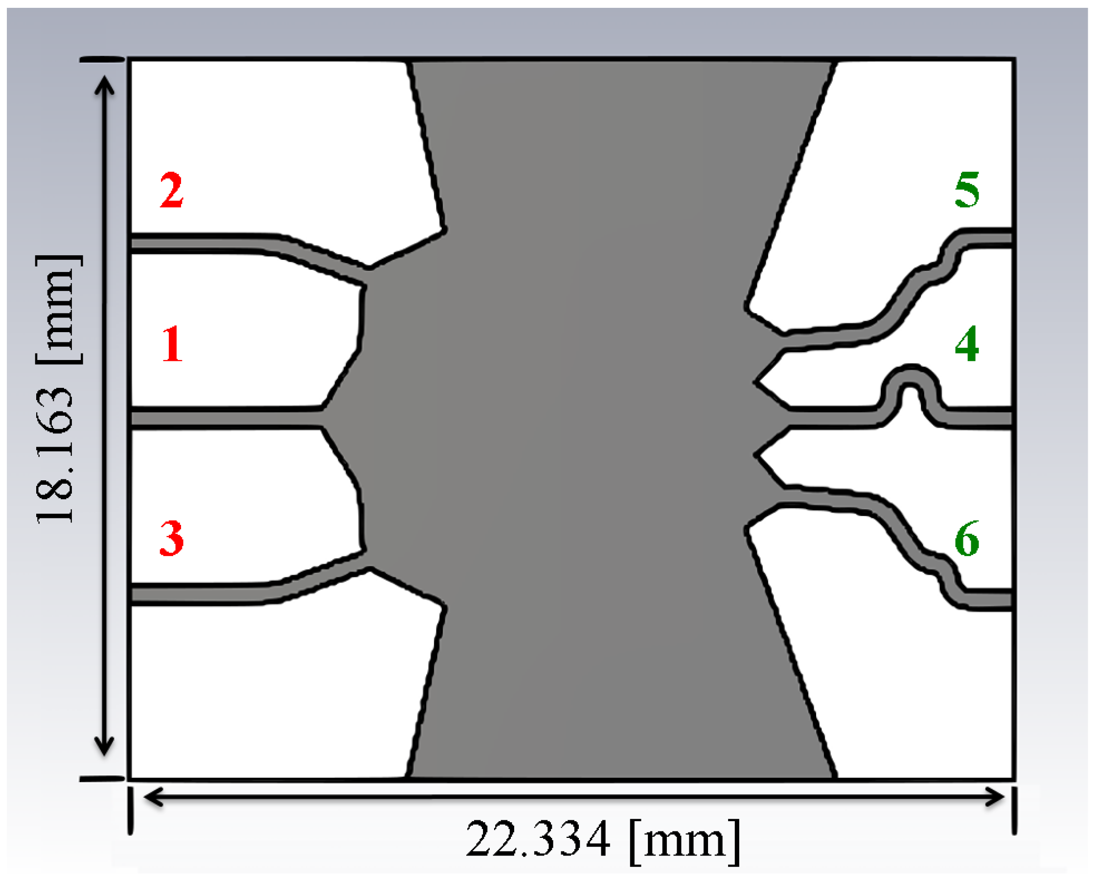
3.2.2. Rotman Lens with Absorbers

Aiming at reducing the unwanted reflections of incident waves in the side walls and enhancing the total efficiency of the lens, the dummy ports are replaced by two absorbing layers covered with metallic shields on each side wall, as shown in Figure 11. The dimensions of this structure are defined as 22.334 × 18.163 × 0.3 mm 3 . The height of the absorbers is equal to the height of the substrate, and their material characteristics are chosen with an ϵ r = 6.15 and a t a n d δ = 0.7 . These material values have been chosen theoretically, by adjusting the value between the initial material and the material is then doped with the conductive molecules as described above. By engineering the substrate, we can efficiently absorb the incident waves and thus attenuate the standing waves of the parallel plate region. Besides, the ultimate scope of this design is to prove that there is an easier to design and implement approach to absorb the incident waves in the side walls than the dummy ports.
Figure 24a–f reveals the improved Rotman lens response in the whole frequency range of 27–33 GHz. This improvement is also justified from the array factor distribution in Figure 25, which is valid in the entire frequency range.

3.2.3. Comparison of the Two Rotman Lens Topologies

The return loss (input reflection coefficient) of the two designed Rotman lenses are depicted in Figure 23 and Figure 26. An improvement by at least 4 dB is clearly observed in the topology with the absorbers, while an acceptable matching over the entire band is offered at the same time. The corresponding coefficients are presented in Figure 21a–f and Figure 24a–f when input ports 1 , 2 , 3 are activated. A reduction in the amplitude variation is first observed. However, the direct path transmission coefficient S 41 is higher. Although a theoretically uniform distribution is sought, higher signal levels at the middle output ports are observed (Figure 21a–f and Figure 24a–f), which yield shaped antenna array aperture excitation and thus lower sidelobes. Furthermore, the observed large amplitude variations in transmission coefficients are degrading the antenna array excitation, as shown in Figure 26. This may be due to the small number of output ports and we expect an improvement in a design with more output ports.
Comparing Figure 21b,d,f and Figure 24b,d,f, the output phase versus frequency linearity is impressively improved when the proposed design of the absorbers is used. Thus, the Rotman design with absorbers provides group delays with smaller variation versus frequency and thus more accurate beamsteering.

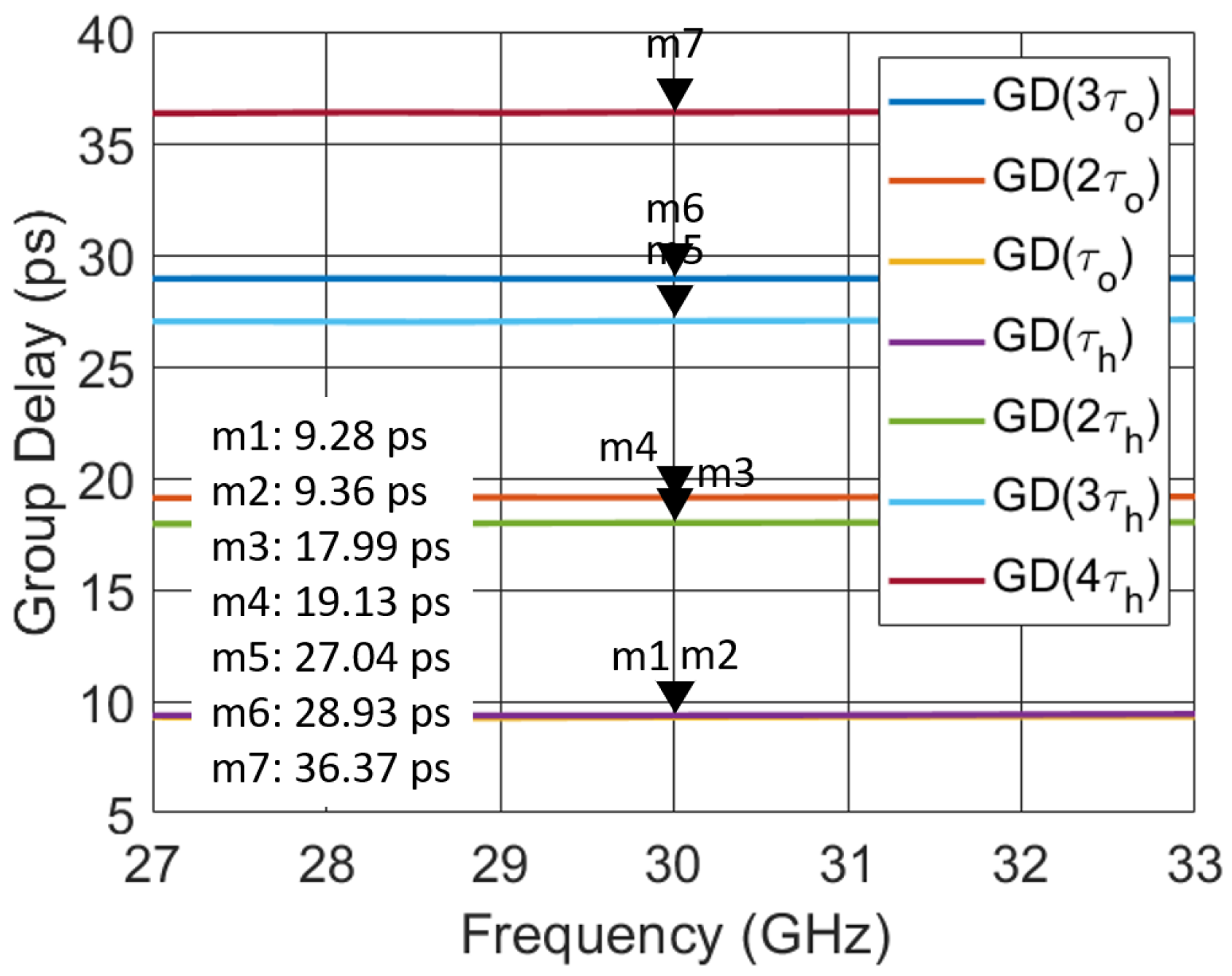
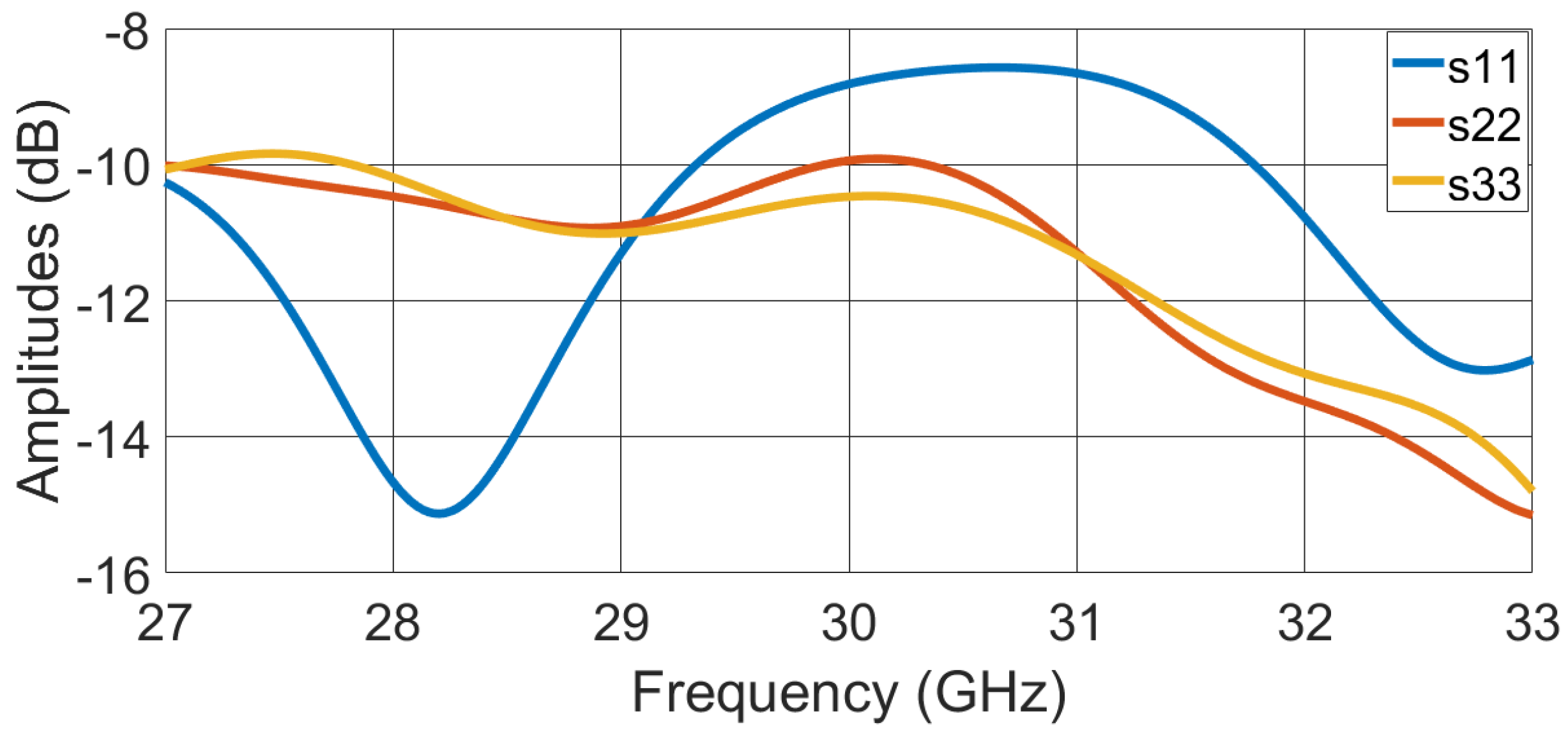
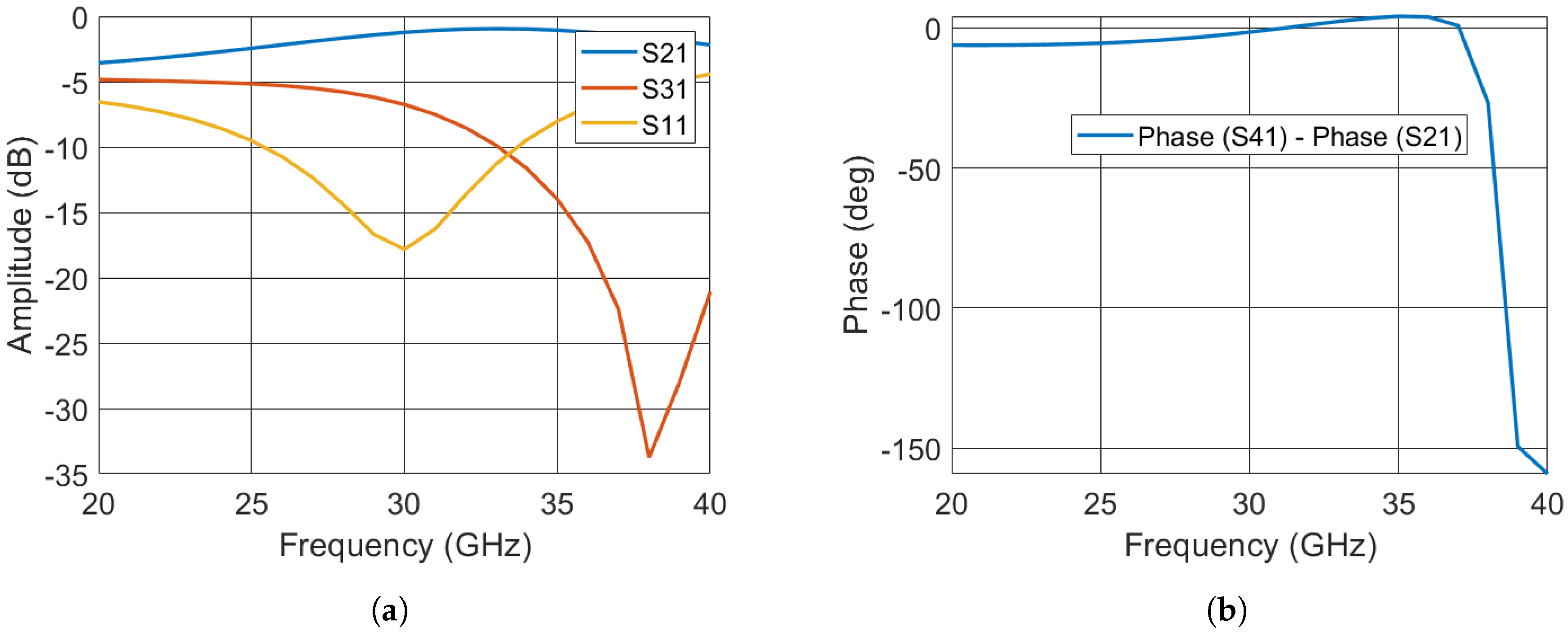
3.3. Tree Topology Results

Figure 13 shows the proposed three-layer tree beamforming network. The implementation of each layer is in stripline technology and the substrate is RT duroid 5870 with ϵ r = 2.33 and t a n δ = 0.0012 . The thickness of each board is 0.127 mm and the signal line of each tree network is sandwiched between two single plated boards, as shown in Figure 27.
All the input ports are located at the bottom layer of the network (see detail in Figure 13). Microstrip to stripline transitions are used for each layer separately. The first tree beamformer is located at the feeding layer and is designed to excite beam 1, as shown in Figure 13. The second tree beamformer at the middle of our multi-layer topology steers the beam to the left and is excited through a via that connects layer 1 with layer 2, as shown in detail in Figure 13. Finally, the third tree beamformer, at the top of our topology, is responsible for the broadside beam and is excited by utilizing two cascaded vertical transitions, as shown in detail in Figure 13.
As mentioned above, the power dividers are of high importance in the proposed topology. Two types of power dividers are incorporated in the network; an equal split Wilkinson power divider [57] and an unequal split power divider as the one reported in [56]. They are both implemented using stripline technology. Figure 28a shows the layout of the equal power divider. As shown in Figure 28b, the reflection coefficient is below 20 dB and the power is equally split through the desired bandwidth. Regarding the unequal power divider (shown in Figure 14), based on the design specifications of our tree topology, a 5-dB power division ratio has to be achieved. To achieve this power division ratio, the divider is designed to have a lower arc of an electrical length of L 1 e = 151.2 ° and an upper arc of L 2 e = 106.21 ° , as shown in Figure 29a. In addition, the lines connecting the 50 Ω resistor to the branches of the divider are designed with electrical lengths of L 3 e = 14.85 ° and L 4 e = 59.95 ° , respectively.
Figure 29a shows the amplitude response of the unequal power division power divider. It can be seen that return loss is kept low for a large bandwidth, whereas the power division ratio limits the bandwidth of this design. As shown in Figure 29b, the phase difference between the two output ports of the divider is approximately equal at the center frequency.
In the proposed design (Figure 13), the physical lengths of the transmission lines connecting the output ports with the unequal power division power dividers on layer 1 are chosen to be 2.36 and 4.05 mm for the left and the right branches, respectively, and they consist of two right angle curved bends. The lengths of the lines connecting the Wilkinson power divider of the first stage to the power dividers of the second stage are 6.24 mm for the left and 2.86 mm for the right branch. In both branches, the arcs attached to the unequal division power divider have a radius of 0.372 mm and an angle of 130 ° . The tree network of layer 2 is a the same as that of layer 1 but mirrored over the vertical axis. Finally, for the tree network in layer 3, the transmission lines connecting the output ports with the unequal power division power dividers again consist of two right angle curved bends, whose combined physical length is 2.36 mm, while the interconnecting lines between the two stages have a total length of 3.02 mm.
Figure 30a–f shows the simulated results of the proposed multilayer tree topology. As shown in Figure 30a, the two middle output ports have similar amplitude responses and are approximately 5 dB higher than the other two ports at the center frequency of 29 GHz. Figure 30b shows the phase differences between the adjacent ports, which are approximately 90 ° with a minor deviation of ± 3 ° at the center frequency. The second tree exhibits similar behavior. Figure 30c shows its amplitude responses where the difference of the two middle ports compared to the two outer ports is approximately 5 dB. The phase differences, similar to the first tree, maintain the required 90 ° between the adjacent ports with a slight deviation of ± 3 ° . Lastly, Figure 30e shows the amplitude distribution for the ports of the third tree topology. As is shown, the amplitudes follow the same trend with cases 1 and 2, while the phase differences, as shown in Figure 30f, are at 0 ° with a minor deviation of ± 3 ° . Figure 31 shows the array factor that was calculated using the S-matrix values of our network. It can be seen that the 19 dB achieved SLL is close to the desired 21 dB. The beam crossover level is at 3 dB and the beams point to broadside, + 30 ° , and 30 ° with negligible deviations.

4. Discussion

Wireless backhaul in mm-Wave bands that offers high speed, wide bandwidth, and several G b p s data rates will be a key component of 5G and early 6G communication systems. As discussed in the Introduction, depending on the channel properties, different communication systems (e.g., beamforming and MIMO) can be accordingly utilized to meet the system requirements, offering the optimal performance. In this work, we develop and show three different beamforming topologies, each with its own advantages and disadvantages, that can be appropriately used on switched beam phased arrays as hybrid beamforming stages. These are designed mainly as proofs of concept with small number of input- and output- ports. Our future work will aim to develop designs that fulfill the practical needs of 5G systems.
First, a novel semi-circular multilayer Blass matrix is proposed (Figure 8). By appropriately choosing the paths of the Blass network, we design a true-time-delay beamforming network aiming to a uniform amplitude distribution. To avoid the high number of crossovers that the typical couplers introduce at its original configuration (e.g., [28]), a double-layer directional coupler [49], is utilized, showing excellent performance throughout the desired band of operation. Notably, a size reduction is achieved compared to a regular Blass design (Figure 3). As shown in Section 3, both the amplitudes and the group delays observed at the output ports are fairly constant for the entire desired frequency band. This response offers an acceptable array factor radiation pattern with a side lobe of at most 10 dB fulfilling the purpose of the current work. For our second true-time-delay beamforming network, a 3 × 3 Rotman lens design is utilized with four dummy ports. To improve the typical poor performance of Rotman lenses with a small number of dummy ports, an innovative technique of field absorbers at the position of its dummy ports is introduced. Specifically, the dielectric substrate that surrounds the area of the dummy ports is doped with a conductive material. By engineering the substrate in this fashion, the dielectric constant remains the same, but its loss tangent increases approximately 10 times, which eliminates in turn the reflections that deteriorate the lens’ performance. Following this design approach, we were able to build a pivotal implementation of a Rotman lens with only four dummy ports, a number that is significantly smaller compared to the typical number of dummy ports used in related works found in the literature [46]. As our last true-time-delay beamforming network, a multi-layer tree topology is introduced for the first time herein (Figure 13). The primary advantage of this topology is the extremely small number of delay lines used along with the corresponding power dividers. Aiming at a Chebyshev amplitude distribution at the excited elements, power dividers of unequal power division are utilized as a proof of concept. As shown in our results for all three beams, there is only a slight phase deviation of ± 3 ° at the center frequency, while the amplitude responses of the outer ports do not deviate more than ± 0.2 dB in respect to the amplitude responses of the center ports, thereby producing a radiation pattern of 19 dB SLL. Notably, even though the tree network is inherently ultra- wideband, since its transmission lines are true time delay elements, the unequal power dividers we use in the proposed design are narrowband. Specifically, the unequal power dividers are limited to operate in a narrow frequency band around the center frequency of 29 GHz thereby making the response of the proposed tree network narrowband as well. However, this is not a big concern, as the specific power divider is only used as a proof of concept and it can be replaced by ultra-wideband unequal power dividers published in the literature (e.g., [58]).

5. Conclusions

Millimeter wave communications have become one of the most promising candidates for the future wireless networks. In this paper, we address the needs of 5G and early 6G wireless communication systems and we explain why hybrid beamforming networks have to be used to address the challenges of these networks and the corresponding channel environments. Specifically, we mention that millimeter wave beamformers are appropriate for switched beam phased arrays as hybrid beamforming stages. Three different true-time-delay analog beamforming networks are developed: a multi-layer Blass matrix, a Rotman lens, and a multi-layer tree topology. For each beamforming network, we develop separately its design methodology as well as analyze its electromagnetic performance, thereby showing their suitability for future communication systems.

Author Contributions

All authors equally contributed to the manuscript. All authors have read and agreed to the published version of the manuscript.

Funding

This work was partially supported by the Air Force Office of Scientific Research under grants FA9550-18-1-0191 and FA9550-19-1-0290.

Conflicts of Interest

The authors declare no conflict of interest.

References

  1. Parvez, I.; Rahmati, A.; Guvenc, I.; Sarwat, A.I.; Dai, H. A Survey on Low Latency Towards 5G: RAN, Core Network and Caching Solutions. IEEE Commun. Surv. Tutor. 2018, 20, 3098–3130. [Google Scholar] [CrossRef]
  2. David, K.; Berndt, H. 6G Vision and Requirements: Is There Any Need for Beyond 5G? IEEE Veh. Technol. Mag. 2018, 13, 72–80. [Google Scholar] [CrossRef]
  3. Li, R. Towards a New Internet for the Year 2030 and Beyond. In Proceedings of the 3rd Annual ITU IMT-2020/5G Workshop and Demo Day, Geneva, Switzerland, 18 July 2018. [Google Scholar]
  4. Strinati, E.C.; Barbarossa, S.; Gonzalez-Jimenez, J.L.; Ktenas, D.; Cassiau, N.; Maret, L.; Dehos, C. 6G: The Next Frontier: From Holographic Messaging to Artificial Intelligence Using Subterahertz and Visible Light Communication. IEEE Veh. Technol. Mag. 2019, 14, 42–50. [Google Scholar] [CrossRef]
  5. Haerick, W.; Gupta, M. 5G and the Factories of the Future. Available online: https://5g-ppp.eu/wp-content/uploads/2014/02/5G-PPP-White-Paper-on-Factories-of-the-Future-Vertical-Sector.pdf (accessed on 13 August 2020).
  6. Huawei. 5G: A Technology Vision. Available online: https://www.huawei.com/ilink/en/download/HW_314849 (accessed on 13 August 2020).
  7. Hossain, E.; Rasti, M.; Tabassum, H.; Abdelnasser, A. Evolution toward 5G multi-tier cellular wireless networks: An interference management perspective. IEEE Wirel. Commun. 2014, 21, 118–127. [Google Scholar] [CrossRef] [Green Version]
  8. Schulz, P.; Matthe, M.; Klessig, H.; Simsek, M.; Fettweis, G.; Ansari, J.; Ashraf, S.A.; Almeroth, B.; Voigt, J.; Riedel, I.; et al. Latency critical IoT applications in 5G: Perspective on the design of radio interface and network architecture. IEEE Commun. Mag. 2017, 55, 70–78. [Google Scholar] [CrossRef]
  9. Johansson, N.A.; Wang, Y.P.E.; Eriksson, E.; Hessler, M. Radio access for ultra-reliable and low-latency 5G communications. In Proceedings of the 2015 IEEE International Conference on Communication Workshop (ICCW), London, UK, 8–12 June 2015; pp. 1184–1189. [Google Scholar]
  10. Lema, M.A.; Antonakoglou, K.; Sardis, F.; Sornkarn, N.; Condoluci, M.; Mahmoodi, T.; Dohler, M. 5G case study of Internet of skills: Slicing the human senses. In Proceedings of the 2017 European Conference on Networks and Communications (EuCNC), Oulu, Finland, 12–15 June 2017; pp. 1–6. [Google Scholar]
  11. Ghosh, A. 5G mmWave Revolution and New Radio. 2017. Available online: https://futurenetworks.ieee.org/images/files/pdf/5GmmWave_Webinar_IEEE_Nokia_09_20_2017_final.pdf (accessed on 13 August 2020).
  12. Ghosh, A.; Maeder, A.; Baker, M.; Chandramouli, D. 5G Evolution: A View on 5G Cellular Technology Beyond 3GPP Release 15. IEEE Access 2019, 127639–127651. [Google Scholar] [CrossRef]
  13. Niu, Y.; Li, Y.; Jin, D.; Su, L.; Vasilakos, A.V. A survey of millimeter wave communications (mmWave) for 5G: Opportunities and challenges. Wirel. Netw. 2015, 21, 2657–2676. [Google Scholar] [CrossRef]
  14. Zhao, Q.; Li, L. Rain attenuation in millimeter wave ranges. In Proceedings of the 2006 7th International Symposium on Antennas, Propagation & EM Theory, Guilin, China, 26–29 October 2006; pp. 1–4. [Google Scholar]
  15. Humpleman, R.J.; Watson, P.A. Investigation of attenuation by rainfall at 60 GHz. Proc. Inst. Electr. Eng. 1978, 125, 85–91. [Google Scholar] [CrossRef]
  16. E-Band Technology. E-band Communications. Available online: http://www.e-band.com/index.php?id=86 (accessed on 13 August 2020).
  17. Rappaport, T.S.; Sun, S.; Mayzus, R.; Zhao, H.; Azar, Y.; Wang, K.; Wong, G.N.; Schulz, J.K.; Samimi, M.; Gutierrez, F. Millimeter wave mobile communications for 5G cellular: It will work! IEEE Access 2013, 1, 335–349. [Google Scholar] [CrossRef]
  18. Pleros, N.; Tsagkaris, K.; Tselikas, N.D. A moving extended cell concept for seamless communication in 60 GHz radio-over-fiber networks. IEEE Commun. Lett. 2008, 12, 852–854. [Google Scholar] [CrossRef]
  19. Mandyan, A. 4G and 5G Capacity Solution, Comparative Study. Available online: https://telecoms.com/intelligence/4g-and-5g-capacity-solutions-comparative-study/ (accessed on 13 August 2020).
  20. Sun, S.; Rappaport, T.S.; Shafi, M.; Tang, P.; Zhang, J.; Smith, P.J. Propagation models and performance evolution for 5G millimeter-wave bands. IEEE Trans. Vehicular Tech. 2018, 67, 8422–8437. [Google Scholar] [CrossRef]
  21. Molisch, A.F.; Ratnam, V.V.; Han, S.; Li, Z.; Nguyen, S.L.H.; Li, L.; Haneda, K. Hybrid Beamforming for Massive MIMO: A Survey. IEEE Commun. Mag. 2017, 55, 134–141. [Google Scholar] [CrossRef] [Green Version]
  22. Rappaport, T.S.; Xing, Y.; MacCartney, G.R.; Molisch, A.F.; Mellios, E.; Zhang, J. Overview of millimeter wave communications for fifth generation (5G) wireless networks-with a focus on propagation models. IEEE Trans. Antennas Propag. 2017, 65, 6213–6230. [Google Scholar] [CrossRef]
  23. Roh, W.; Seol, J.Y.; Park, J.; Lee, B.; Lee, J.; Kim, Y.; Cho, J.; Cheun, K.; Aryanfar, F. Millimeter-Wave beamforming as an enabling technology for 5G cellular communications: The oretical feasibility and prototype results. IEEE Commun. Mag. 2017, 52, 106–113. [Google Scholar] [CrossRef]
  24. Cameron, T. RF Technology for 5G Mmwave Radios. Available online: /https://www.analog.com/media/en/technical-documentation/white-papers/RF-Technology-for-the-5G-Millimeter-Wave-Radio.pdf (accessed on 13 August 2020).
  25. Ali, E.; Ismail, M.; Nordin, R.; Abdullah, N.F. Beamforming techniques for massive MIMO systems in 5G: Overview, classification, and trends for future research. Front. Inf. Technol. Electron. Eng. 2017, 18, 753–772. [Google Scholar] [CrossRef]
  26. Ahmed, I.; Khammari, H.; Shahid, A.; Musa, A.; Kim, K.S.; De Poorter, E.; Moerman, I. A Survey on Hybrid Beamforming Techniques in 5G: Architecture and System Model Perspectives. IEEE Commun. Surv. Tutor. 2018, 20, 3060–3097. [Google Scholar] [CrossRef] [Green Version]
  27. Butler, J.; Lowe, R. Beam forming matrix simplifiers design of electrically scanned antennas. Electron. Des. 1961, 9, 170–173. [Google Scholar]
  28. Blass, J. Multidirectional antenna—A new approach to stacked beams. In Proceedings of the 1958 IRE International Convention Record, New York, NY, USA, 21–25 March 1966; pp. 48–50. [Google Scholar] [CrossRef]
  29. Nolen, J. Synthesis of Multiple Beam Networks for Arbitrary Illuminations. Ph.D. Thesis, Radio Division, Bendix Corporation, Baltimore, MD, USA, 1965. [Google Scholar]
  30. Rotman, W.; Turner, R. Wide-angle microwave lens for line source applications. IEEE Trans. Antennas Propag. 1963, 11, 623–632. [Google Scholar] [CrossRef]
  31. Wincza, K.; Staszek, K.; Gruszczynski, S. Broadband Multibeam Antenna Arrays Fed by Frequency-Dependent Butler Matrices. IEEE Trans. Antennas Propag. 2017, 65, 4539–4547. [Google Scholar] [CrossRef]
  32. Djerafi, T.; Wu, K. A Low-Cost Wideband 77-GHz Planar Butler Matrix in SIW Technology. IEEE Trans. Antennas Propag. 2012, 60, 4549–4954. [Google Scholar] [CrossRef]
  33. Fakoukakis, F.E.; Kaifas, T.; Vafiadis, E.E.; Kyriacou, G.A. Design and implementation of Butler matrix-based beam-forming networks for low sidelobe level electronically scanned arrays. Int. J. Microw. Wirel. Technol. 2015, 7, 69–79. [Google Scholar] [CrossRef]
  34. Fakoukakis, F.E.; Kyriacou, G.A. Novel Nolen Matrix Based Beamforming Networks for Series-Fed Low SLL Multibeam Antennas. Prog. Electromagn. Res. B 2013, 51, 33–64. [Google Scholar] [CrossRef] [Green Version]
  35. Chen, Q.P.; Zheng, S.Y.; Long, Y.; Ho, D. Design of a Compact Wideband Butler Matrix Using Vertically Installed Planar Structure. IEEE Trans. Components Packag. Manuf. Technol. 2018, 8, 1420–1430. [Google Scholar] [CrossRef]
  36. Nedil, M.; Denidni, T.A.; Talbi, L. Novel butler matrix using CPW multilayer technology. IEEE Trans. Microw. Theory Tech. 2006, 54, 499–507. [Google Scholar] [CrossRef]
  37. Cao, Y.; Chin, K.; Che, W.; Yang, W.; Li, E.S. A Compact 38 GHz Multibeam Antenna Array With Multifolded Butler Matrix for 5G Applications. IEEE Antennas Wirel. Propag. Lett. 2017, 16, 2996–2999. [Google Scholar] [CrossRef]
  38. Tornielli di Crestvolant, V.; Martin Iglesias, P.; Lancaster, M.J. Advanced Butler Matrices With Integrated Bandpass Filter Functions. IEEE Trans. Microw. Theory Tech. 2015, 63, 3433–3444. [Google Scholar] [CrossRef] [Green Version]
  39. Dyab, W.M.; Sakr, A.A.; Wu, K. Dually-Polarized Butler Matrix for Base Stations With Polarization Diversity. IEEE Trans. Microw. Theory Tech. 2018, 66, 5543–5553. [Google Scholar] [CrossRef]
  40. Tamayo-Domínguez, A.; Fernández-González, J.; Sierra-Castañer, M. 3-D-Printed Modified Butler Matrix Based on Gap Waveguide at W-Band for Monopulse Radar. IEEE Trans. Microwave Theory Tech. 2020, 68, 926–938. [Google Scholar] [CrossRef]
  41. Fonseca, N.J. Printed S-Band 4 × 4 Nolen Matrix for Multiple Beam Antenna Applications. IEEE Trans. Antennas Propag. 2009, 57, 1673–1678. [Google Scholar] [CrossRef]
  42. Djerafi, T.; Fonseca, N.J.G.; Wu, K. Broadband Substrate Integrated Waveguide 4 × 4 Nolen Matrix Based on Coupler Delay Compensation. IEEE Trans. Microw. Theory Tech. 2011, 59, 1740–1745. [Google Scholar] [CrossRef]
  43. Ren, H.; Zhang, H.; Li, P.; Gu, Y.; Arigong, B. A Novel Planar Nolen Matrix Phased Array for MIMO Applications. In Proceedings of the 2019 IEEE International Symposium on Phased Array System & Technology (PAST), Waltham, MA, USA, 15–18 October 2019; pp. 1–4. [Google Scholar] [CrossRef]
  44. Chu, T.-S.; Hossein, H. True time delay based multi-beam arrays. IEEE Trans. Microw. Theory Tech. 2013, 61, 3072–3081. [Google Scholar] [CrossRef]
  45. Lambrecht, A.; Beer, S.; Zwick, T. True-time-delay beamforming with a Rotman-lens for ultrawideband antenna systems. IEEE Trans. Antennas Propag. 2010, 10, 3189–3195. [Google Scholar] [CrossRef]
  46. Merola, C.S.; Vouvakis, M.N. Massive MIMO Beamforming on a Chip. In Proceedings of the 2019 IEEE International Symposium on Antennas and Propagation and USNC-URSI Radio Science Meeting, Atlanta, GA, USA, 7–12 July 2019; pp. 1477–1478. [Google Scholar]
  47. Hansen, R.C. Microwave Scanning Antennas: Array Systems; Academic Press: Cambridge, MA, USA, 1964. [Google Scholar]
  48. Pozar, D.M. Microwave Engineering; Wiley: Hoboken, NJ, USA, 2012. [Google Scholar]
  49. Tanaka, T.; Tsunoda, K.; Aikawa, M. Slot–coupled directional couplers on a both–sided substrate MIC and their applications. Electron. Comm. Jpn. Part II 1989, 72, 91–99. [Google Scholar] [CrossRef]
  50. Wong, M.F.; Hanna, V.F.; Picon, O.; Baudrand, H. Analysis and design of slot-coupled directional couplers between double-sided substrate microstrip lines. In Proceedings of the 1991 IEEE MTT-S International Microwave Symposium Digest, Boston, MA, USA, 10–14 June 1991; Volume 2, pp. 755–758. [Google Scholar] [CrossRef]
  51. Balanis, C.A. Antenna Theory: Analysis and Design, 3rd ed.; John Wiley: Hoboken, NJ, USA, 2005. [Google Scholar]
  52. Vashist, S.; Soni, M.K.; Singhal, P.K. A Review on the Development of Rotman Lens Antenna. Chin. J. Eng. 2014, 2014, 1–9. [Google Scholar] [CrossRef] [Green Version]
  53. Sbarra, E.; Marcaccioli, L.; Gatti, R.V.; Sorrentino, R. A novel rotman lens in SIW technology. In Proceedings of the 2007 European Radar Conference, Munich, Germany, 10–12 October 2007; pp. 236–239. [Google Scholar] [CrossRef]
  54. Yao, J. Microwave Photonics. J. Lightwave Technol. 2009, 27, 314–335. [Google Scholar] [CrossRef]
  55. Mailloux, R.J. Phased Array Antenna Handbook, 3rd ed.; Artech House, Inc.: Norwood, MA, USA, 2017. [Google Scholar]
  56. Qi, T.; He, S.; Dai, Z.; Shi, W. Novel Unequal Dividing Power Divider With 50 Ω Characteristic Impedance Lines. IEEE Microw. Wirel. Components Lett. 2016, 26, 180–182. [Google Scholar] [CrossRef]
  57. Wilkinson, E.J. An N-Way Hybrid Power Divider. Ire Trans. Microw. Theory Tech. 1960, 8, 116–118. [Google Scholar] [CrossRef]
  58. Chen, J.; Xue, Q. Novel 5to1 Unequal Wilkinson Power Divider Using Offset Double-Sided Parallel-Strip Lines. IEEE Microw. Wirel. Compon. Lett. 2007, 17, 175–177. [Google Scholar] [CrossRef]
Figure 1. Illustration of different 5G communication cells.
Electronics 09 01331 g001
Figure 2. Hybrid beamforming architecture.
Electronics 09 01331 g002
Figure 3. Blass matrix schematic.
Electronics 09 01331 g003
Figure 4. Circular Blass matrix topology.
Electronics 09 01331 g004
Figure 5. Traditional implementations of directional cross couplers: (a) multi-section branch line cross-coupler; and (b) Lange directional coupler.
Electronics 09 01331 g005
Figure 6. Layout of the dual-layer directional coupler.
Electronics 09 01331 g006
Figure 7. Frequency response of the double layer directional coupler: (a) amplitude response; and (b) phase difference between the output ports of the double layer directional coupler.
Electronics 09 01331 g007
Figure 8. Layout of the proposed circular mm-Wave Blass matrix topology.
Electronics 09 01331 g008
Figure 9. Principle Rotman lens architecture.
Electronics 09 01331 g009
Figure 10. Proposed Rotman lens architecture with three inputs (red), three outputs (green), and four dummy (D) ports (blue) in the side walls. The scale is 10:3.06 mm.
Electronics 09 01331 g010
Figure 11. Rotman lens architecture with three inputs (red), three outputs (green), and two absorbers in the side walls. The scale is 10:3.06 mm.
Electronics 09 01331 g011
Figure 12. Schematic of the hierarchical true time delay tree beamformer: (a) 1 to 4; and (b) 1 to 8.
Electronics 09 01331 g012
Figure 13. Multilayer tree topology layout.
Electronics 09 01331 g013
Figure 14. Layout of unequal power divider.
Electronics 09 01331 g014
Figure 15. Schematic of the tree type network with N outputs.
Electronics 09 01331 g015
Figure 16. Blass matrix cross section.
Electronics 09 01331 g016
Figure 17. Group delay response of the delay lines of the Blass matrix.
Electronics 09 01331 g017
Figure 18. Example of array fed by the Blass matrix.
Electronics 09 01331 g018
Figure 19. Proposed Blass matrix simulation results: (a,c,e) amplitudes | S i j | for the i = 1 4 outputs when the input ports j = 1 , 2 , 3 are excited; and (b,d,f) group delay for the i = 1 4 outputs when input ports j = 1 , 2 , 3 are excited.
Electronics 09 01331 g019
Figure 20. Calculated array factor radiation pattern when the outputs of the proposed Blass matrix (Figure 8) is used to excite the phased array at: (a) 27 GHz; (b) 29 GHz; (c) 31 GHz; and (d) 33 GHz.
Electronics 09 01331 g020
Figure 21. Ordinary Rotman lens with 4 dummy ports simulation results: (a,c,e) amplitudes | S i j | for the i = 1 3 outputs when the input ports j = 1 , 2 , 3 are excited; and (b,d,f) group delay for the i = 1 3 outputs when input ports j = 1 , 2 , 3 are excited.
Electronics 09 01331 g021
Figure 22. Calculated array factor radiation patterns at 27 GHz and 30 GHz when the outputs of the proposed Rotman lens (Figure 10) are used to excite the phased array.
Electronics 09 01331 g022
Figure 23. Ordinary Rotman lens with 4 dummy ports reflection coefficients.
Electronics 09 01331 g023
Figure 24. Proposed Rotman lens with absorbers in the side walls simulation results: (a,c,e) amplitudes | S i j | for the i = 1 3 outputs when the input ports j = 1 , 2 , 3 are excited; and (b,d,f) group delay for the i = 1 3 outputs when input ports j = 1 , 2 , 3 are excited.
Electronics 09 01331 g024
Figure 25. Calculated array factor radiation pattern when the outputs of the proposed Rotman lens (Figure 11) are used to excite the phased array.
Electronics 09 01331 g025
Figure 26. Proposed Rotman lens with absorbers in the side walls reflection coefficients.
Electronics 09 01331 g026
Figure 27. Cross section of the multilayer tree beamforming network.
Electronics 09 01331 g027
Figure 28. Equal power Wilkinson power divider: (a) layout of the equal power split Wilkinson power divider; and (b) amplitude response of the equal power split Wilkinson power divider.
Electronics 09 01331 g028
Figure 29. Response of the unequal split power divider: (a) amplitudes of the unequal split power divider output ports; and (b) phase difference between the unequal split power divider output ports.
Electronics 09 01331 g029
Figure 30. Simulated results of the 3D tree beamformer: (a,c,e) amplitude of the s-parameters for the bottom top and middle network respectively; and (d,e,f) the phase by the s-parameters for the bottom, top and middle network, respectively.
Electronics 09 01331 g030
Figure 31. Calculated array factor of the tree topology.
Electronics 09 01331 g031

