3.1. Sub-Array Design
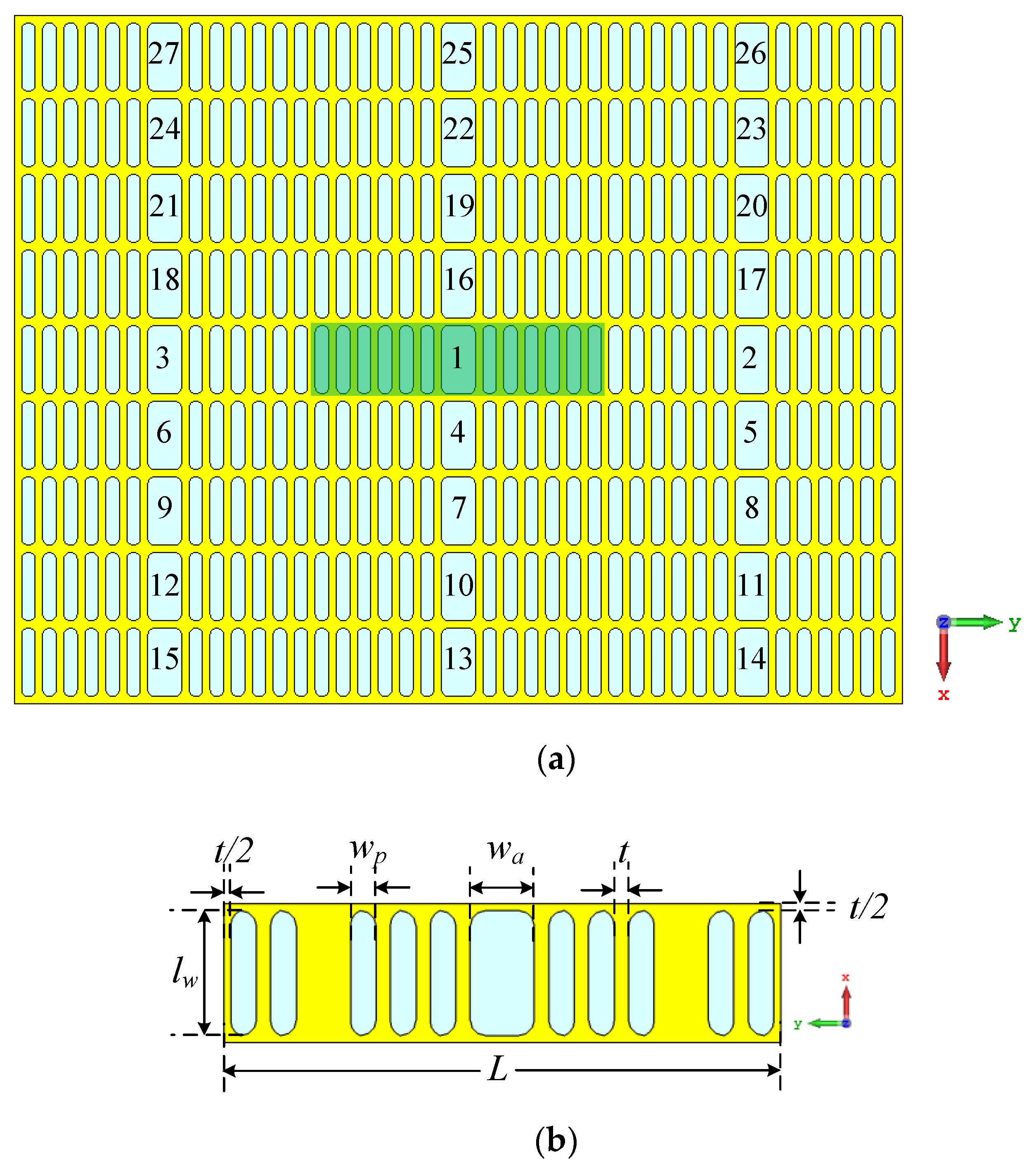
In this paper, we design a planar array built up from linear sub-arrays. The sub-arrays have to support a wide scan range in the H-plane with a reduced scanning capability in the E-plane. The design starts from the structure of
Figure 2a, where a linear antenna sub-array of N
E = 13 open-ended waveguides is placed in an N
A = 9 × 3 array configuration.
The length of the sub-array, L = 2.653λ0, with λ0 denoting the free-space wavelength, was chosen in such a way as to achieve a FoV of about ±8°. The choice of the length, lw = 0.6λ0, of the waveguides is governed by the cut-off condition of the fundamental TE01 mode, that is lw > 0.5λ0. The width of the passive waveguides, wp = 0.12λ0, the thickness of the walls, t = 0.0679λ0, as well as the relevant rounding radius of 0.8 mm were chosen so as to simplify the manufacturing process. Finally, the width of the central waveguide, wa = 0.3λ0, is optimized in a way to achieve good impedance matching characteristics. At the initial design step, the length of all the waveguides is set to 0.1λg, where λg denotes the guided wavelength of the fundamental TE01 mode of the passive waveguides. At the working frequency, f0 = 28.0 GHz, and for the specified waveguide dimensions, we get λg = 21.104 mm.
In a linear array, the angular position of the grating lobes is a function of the separation
d between antenna elements and the scan angle
θ0, and is given by:
where
p = ±1, ±2,… is chosen in such a way as to define an angle with real value, as per the condition |sin
θp| ≤ 1. The maximum scan angle of the array factor before the appearance of the first grating lobe in the field of view is
θp = −
θ0.
Using Equation (3), we can evaluate the maximum theoretical scan range in the two main planes of the array of sub-arrays in
Figure 2, which is ±10.86° along the Ε-plane and ±48.47° along the H-plane. Therefore, theoretically, in order to maximize the gain flatness and minimize the radiation to the undesired directions, the sub-array embedded radiation pattern has to have a high gain flat-top shape in the calculated scan range and should have a low gain outside this range. However, a radiation pattern with such a jump discontinuity in the relevant gain distribution cannot be synthesized using a limited-size array, unless we introduce a transition region which, however, reduces the maximum scan range.
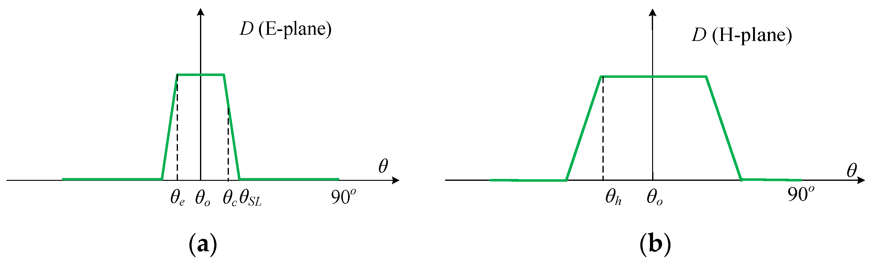
Therefore, on the basis of this observation, the flat-top region has been set to ±8.0° and ±40.0° along the E-plane and the H-plane, respectively. Additional design goals are enforced so as to achieve maximal directivity along the boresight, low side-lobe levels (SLL < −15 dB) along the E-plane, and high return loss combined with low coupling coefficients at the active ports of the array at the central operating frequency. Equation (4) shows the objective function used for the optimization:
where the first term is to minimize
,
j = 1,2,…,
Na, and, in this way, optimize the scattering parameters of the central sub-array. The second term maximizes the broadside directivity. The next two terms are introduced to maximize the flat-top regions, with
θh = 40° and
θe = 8°, along the H-plane and E-plane, respectively. Finally, the last two terms are useful to minimize the directivity outside the field of view along the E-plane, the relative directivity at the critical angle
θc = 14°, and the SLL for
θ ∈ [
θSL, 90°] with
θSL = 20°. The designed sub-array is symmetrical with boresight radiation pattern characteristics along the
z-axis. Therefore, we can confine the optimization process to the angular range
φ ∈ [
θSL, 90°].
Figure 3 shows graphically the defined angular regions.
Utilizing the objective function defined in Equation (4), the design procedure is turned into the solution of the following minimization problem:
Due to the symmetry of the considered sub-array structure, the number of design parameters is equal to half the number of passive waveguides embedded in each individual sub-array.
The optimization procedure starts with the calculation of the embedded element patterns and scattering matrix of an array of 9 × (3 × 13) elements. To this end, a suitable full-wave electromagnetic solver is used [
14]. The obtained results are then imported into an in-house developed dedicated software that implements the proposed design procedure. Next, using Equations (1) and (2), the objective function of Equation (4) is implemented. Then, the Global Search Optimization routine embedded in Matlab [
13] is adopted to address the minimization problem described by Equation (5). The Global Search Optimization technique combines a global pattern-search-based optimizer with a local gradient-based optimization algorithm. Details of the Global Search Optimization algorithm can be found in [
15].
The optimal positions of the short-circuits along the passive waveguides are listed in
Table 1, where the waveguides have been numbered starting from the closest one to the central active element. A cross-section of the resulting array is shown in
Figure 4.
The electromagnetic characteristics of the designed sub-array structure have been successfully validated by using a full-wave solver [
14]. After the optimization procedure, the number of sub-arrays has been gradually increased until the radiation pattern of the central sub-array does not change significantly any longer.
Figure 5 shows the three main cuts of the embedded radiation pattern of the central sub-array when integrated in 9 × 3, 11 × 5, and 15 × 9 array configurations.
In
Figure 5, one can notice a non-negligible change in the embedded radiation patterns along the E- and D-planes when the array size is increased from 9 × 3 to 11 × 5 sub-array elements. More specifically, even though the half-power beam-width does not vary along the H-plane, it differs significantly along the other planes, by 0.3° along the E-plane and by 1.3° along the D-plane. Furthermore, a large deviation of about 7.8 dB is observed in the sidelobe level along the E-plane. No meaningful performance variations occur for further increases of the array size, i.e., to 15 × 9 elements. As a matter of fact, the maximal difference inside the half-power beam-width along the various planes is about 0.1 dB, whereas the deviation in terms of the sidelobe level is negligible. An additional investigation has been performed on the active reflection coefficient of the central sub-array element in the 9 × 3, 11 × 5, and 15 × 9 array topologies. As it appears in
Figure 6, the active reflection coefficients featured by the central elements of the 11 × 5 and 15 × 9 arrays show rather similar behavior but differ quite significantly from the one obtained for the 9 × 3 array. On the basis of the reported results, the radiation pattern of the central element of the 11 × 5 array has been selected as the embedded sub-array pattern, whose main parameters are detailed in
Table 2.
From
Figure 5b and
Table 2, it can be concluded that the scan range along the E-plane is close to the optimization objective, whereas a gap is observed in relation to the scan range along the H-plane. The sub-array directivity for
θ0 = 0° is 15.7 dBi, which is 2.3 dB higher than the nominal directivity calculated on the basis of the physical aperture area
Aap of the individual sub-array, that is:
We can conclude that the sub-array directivity has been enhanced thanks to the overlapping with adjacent sub-arrays. This increase in directivity can be translated in a 41% reduction of the required transmit power or, equivalently, a 23% reduction in the number of required sub-arrays. In order to provide an insight into the process that is responsible for the enhancement of the directivity, the electric field distribution over the radiating aperture of the 11 × 5 array is reported in
Figure 7 when only the central sub-array is active and the other sub-arrays are terminated on matched loads.
From
Figure 7, it can be seen that the electric field propagates in a very effective way towards adjacent sub-arrays virtually in all directions. Effectively, all the sub-arrays contribute, to some extent, to the electromagnetic field radiation process. This mechanism enables the sub-array overlapping and, from there, the mentioned directivity enhancement and capability of synthesizing complex-shaped radiation pattern. It should be noted however that, while propagating, the electromagnetic field gradually decays and eventually displays a limited intensity along the edge elements of the array. This is the reason why a further increase in the number of sub-arrays (beyond the size of 11 × 5) does not significantly affect the central sub-array characteristics.In
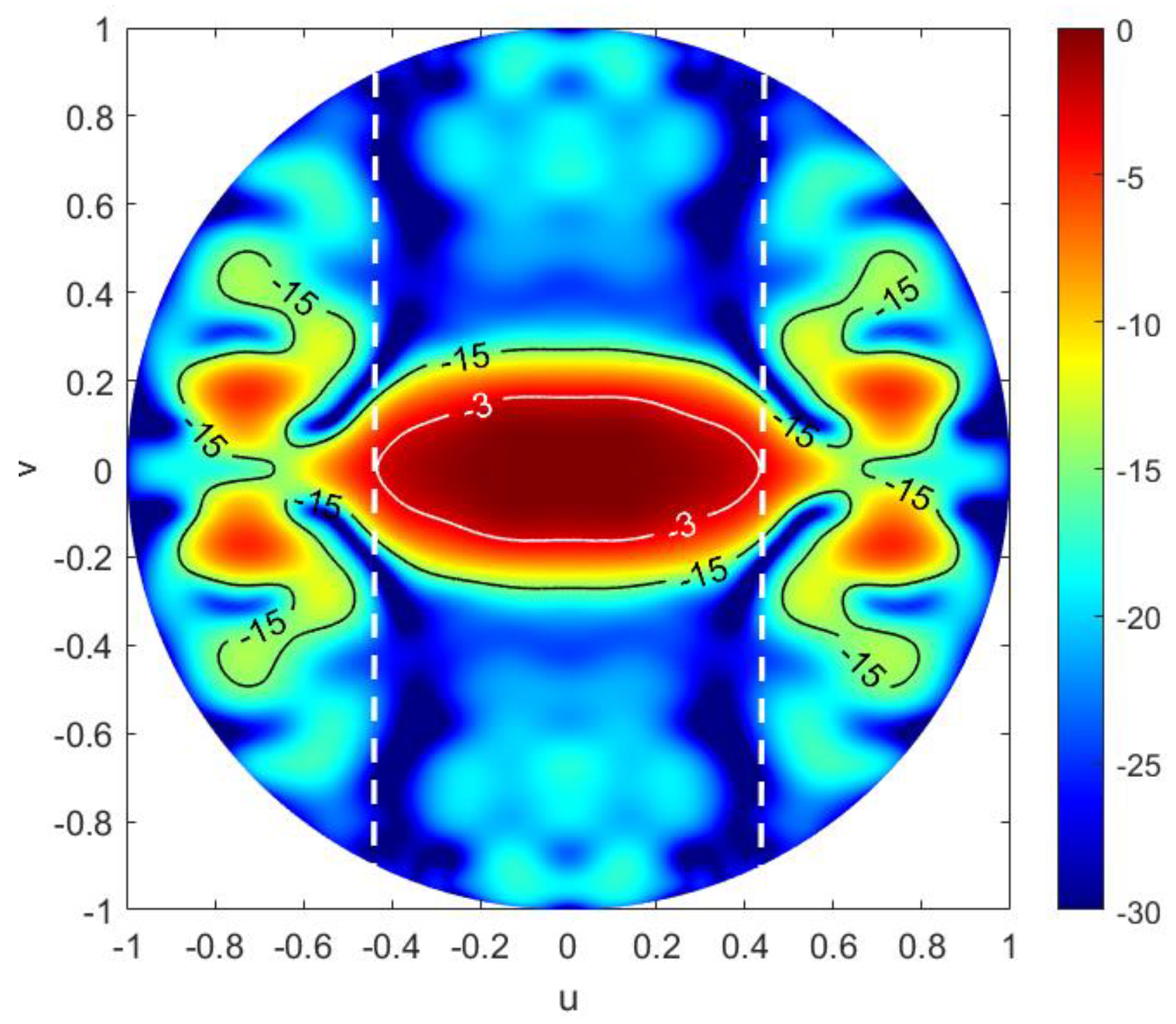
Figure 8, the embedded radiation pattern of the central sub-array of the 11 × 5 element array is presented in the uv-plane, where u = sinθcosφ and v = sinθsinφ.
Figure 8 shows that the areas where the SLL is larger than −15 dB are outside the region defined by the vertical dotted lines. This region identifies the angular sector where the grating lobes would occur assuming that the considered sub-array is used in a uniform planar array configuration. The performance of such an array can be estimated by analyzing the embedded sub-array pattern presented in
Figure 8. Along the H-plane, the grating lobes are outside the visible region over the entire scan range. However, along the E-plane, the grating lobes are inside the visible region. In order to achieve a 10 dB grating-lobe rejection level, we have to limit the scan range to ±8.7°. On the other hand, if a 15 dB grating-lobe rejection level is enforced, the scan range shrinks further to ±6.5°.
The active voltage standing wave ratio (VSWR) versus frequency and scan angle of the central sub-array of the 11 × 5 array configuration is shown in
Figure 9.
Figure 9 shows that the designed sub-array is intrinsically matched, though the relevant impedance matching band shifts with the scan angle. The maximum scanning range can be obtained on the basis of application-specific requirements for active VSWR and bandwidth. In case, where broadband behavior is needed, the integration of a suitable impedance matching network can be explored. The design of such a matching network is outside the scope of this work.
3.2. Array Design
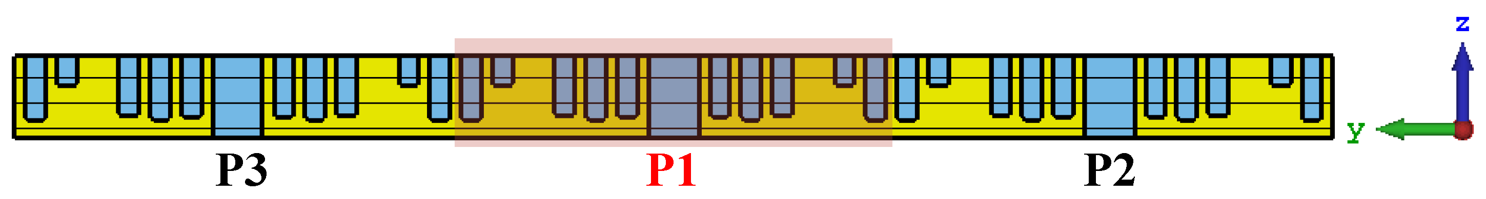
In this section, we use the designed sub-array to realize an antenna array that features a rotationally symmetric mainbeam with a high directivity level of at least 46 dBi. To achieve these goals, a planar array of 65 × 19 elements is required. The simplest approach to the design of such an array would be to adopt the same embedded radiation pattern of the central sub-array analyzed in the previous section for all the array elements. However, this approach would not account for the fact that the edge elements experience different surroundings and, therefore, are characterized by different embedded radiation patterns. A more accurate design approach consists in the use of the embedded radiation pattern of the edge elements of the small array as an approximation of the one relevant to the edge elements of the large array, as illustrated schematically in
Figure 10.
The transformation from the 11 × 5 to the 65 × 19 array configuration is performed as follows:
The radiation pattern of the central element of the 11 × 5 array (red element in
Figure 10a is used to synthesize the central 55 × 15 sub-array (highlighted in red in
Figure 10b).
The elements highlighted in orange in a are used to synthesize the corresponding domains with 55 × 1 sub-arrays highlighted in orange in
Figure 10b.
Similarly to step 2, the blue elements in
Figure 10a are used to synthesize the domains of 1 × 15 sub-arrays highlighted in blue in
Figure 10b.
Finally, the remaining green elements in
Figure 10a are used as is to complete the 65 × 19 array in
Figure 10b.
The scan characteristics along the two principal planes of the resulting 65 × 19 array are illustrated in
Figure 11. The achieved boresight directivity level is 46.5 dBi, which is 0.1 dBi smaller than that displayed by the 65 × 19 array when the embedded radiation pattern of the central sub-array is used for all the elements and, therefore, the edge effect is neglected. It is worth noting, also, that the edge effect causes faster decay of the array mainbeam with the scanning angle, as it can be observed in
Figure 11. In the absence of the edge effect, the array mainbeam would follow the profile of the central sub-array pattern. This non-ideality is responsible for a reduced scan range, which can be quantified as 7.5° in the E-plane, and 24.2° in the H-plane.
To show the impact of the edge effect on the side-lobe level characteristics, the array radiation pattern evaluated using the proposed design approach for the scan angles of 25° and 7.5° along the H- and E-plane, respectively, has been compared against the corresponding one obtained when the radiation pattern of the central sub-array is used for all elements of the array; therefore, the edge effects are neglected (see
Figure 12).
As it can be noticed in
Figure 12, neglecting the edge effect leads to an overestimation of the main-beam directivity, by 0.7 dB in the H-plane, and by 1.6 dB in the E-plane, respectively. The deviation along the E-plane is more noticeable because of the smaller number, 19, of sub-arrays in that direction, as compared to the number of elements, 65, along the H-plane. Another effect of the edge elements that can be observed in
Figure 12 is relevant for the increase of the sidelobe levels, by about 14.6 dB for
−25.0° along the H-plane, and by about 7.5 dB for
−7.5° along the E-plane. The performed comparison clearly shows the importance of including the edge effects in the analysis of the array performance.
The filtering effect of the sub-array factor for various scan angles is visualized in
Figure 13e–h. For comparison, the array factor of a 65 × 19 array is presented in
Figure 13a–d.
Figure 13a–d shows the array factor of a 65 × 19 array for various representative scanning angles. The array elements are excited with uniform amplitude, whereas the phase tapering is optimized so to steer the array beam along the desired direction. Because of the large distance between array elements along the u-axis, grating lobes appear. On the other hand, the array element separation along the v-axis is smaller than 0.6λ
0 that is instrumental in keeping the grating lobes outside the visible region, as per Equation (3), for the targeted scanning range.
Figure 13e–h shows the filtering effect on the sub-array radiation pattern that is useful in the suppression of undesired grating lobes. It is worth mentioning that even though the sidelobe level of the embedded sub-array pattern is very high in some specific directions, as is shown in
Figure 8, the radiation pattern of the total array has a sidelobe level below −30 dB, at the specified directions. This performance is achieved thanks to the fact that the array scanning is restricted to the angular region defined by the contour line at −3 dB level. Therefore, it has been shown that the requirement on the sub-array side lobe level can be relaxed for certain directions which are defined by the scan range of the full array. Finally, due to the uniform amplitude excitation, the side-lobe level of the total radiation pattern is about −13.27 dB. If further sidelobe level reduction is required, a suitable amplitude tapering scheme of the array excitation has to be adopted [
16].


