Article

Design of an Ultra-Wideband Microstrip-to-Slotline Transition on Low-Permittivity Substrate

1
School of Electronics Engineering, Kyungpook National University, Daegu 41566, Korea
2
Research Institute for Microwave and Millimeter-Wave Studies, National University of Sciences and Technology, Islamabad 44000, Pakistan
*
Author to whom correspondence should be addressed.
Electronics 2020, 9(8), 1329; https://doi.org/10.3390/electronics9081329
Submission received: 23 July 2020 / Revised: 12 August 2020 / Accepted: 13 August 2020 / Published: 17 August 2020
(This article belongs to the Special Issue Ultra-Wideband Microwave/MM-Wave Components and Packaging)

Abstract

:
Analysis and design of an ultra-wideband microstrip-to-slotline transition on a low permittivity substrate is presented. Cross-sectional structures along the proposed transition are analyzed using conformal mapping assuming quasi-TEM modes, attaining one analytical line impedance formula with varying design parameters. Although the slotline is a non-TEM transmission line, the transitional structures are configured to have quasi-TEM modes before forming into the slotline. The line impedance is optimally tapered using the Klopfenstein taper, and the electric field shapes are smoothly transformed from microstrip line to slotline. The analytical formula is accurate within 5% difference, and the final transition configuration can be designed without parameter tuning. The implemented microstrip-to-slotline transition possesses insertion loss of less than 1.5 dB per transition and return loss of more than 10 dB from 4.4 to over 40 GHz.

1. Introduction

With the advent of the 4th industrial revolution and the 5th generation mobile communication, the amount of data tends to increase rapidly, thus requiring various microwave components with wide bandwidth. High-speed digital signals typically occupy wide spectrum, necessitating very wideband transmission lines and transitions in order not to distort the signal shapes, preserving the signal integrity. Various planar transmission lines can be formed in multi-layered circuit boards, and each transmission line has unique advantages and limits. Therefore, good performing transitional structures connecting these planar transmission lines are more and more demanded.
A microstrip line (MSL) is an unbalanced transmission line supporting a quasi-TEM mode, and is most-frequently used in the microwave and mm-wave circuits. The electric field lines are shaped from a top signal conductor to the bottom ground plane mostly in vertical patterns, and achievable line impedance ranges from 20 Ω to 100 Ω. A slotline, on the other hand, is a complementary structure to the microstrip line, and has two wide conductor planes separated by a gap, formed on the top side of the substrate. The mode of propagation in the slotline is a non-TEM mode, and almost TE mode without a cutoff frequency [1]. The electric field lines are concentrated mostly in horizontally patterns between the two conductor planes, and achievable line impedance ranges from 50 Ω to 200 Ω [1]. In order to design a good-performing ultra-wideband transition from microstrip line to slotline, the line impedance along the stretch of the transition should be optimally matched, and the electric field line shapes should be smoothly transformed to conform the change of line modes.
A typical microstrip-to-slotline transition used a cross junction to magnetically couple between the two lines: i.e., using a perpendicularly crossing structure with quarter-wave stubs on both lines [1,2,3]. The resonating structure caused frequency bandwidth limitation, and efforts have been made to minimize the structure or widen the frequency bandwidth [4,5,6,7,8,9,10]. By using a multi-arm single junction or a strip-slot double junction structure, the transition bandwidth could be widened, but the structure was very sensitive to fabrication tolerances and needed high-permittivity substrates to reduce the parasitic capacitance [6,7]. In addition, for use as a compact balun of an antenna, several transition designs were attempted with a slotted microstrip structure or a novel shape stub [9,10]. Another type of transition was designed with bifurcated microstrip lines, and used a half-wave-delayed microstrip line to feed the slotline [11]. The structure was uniplanar and had compact size, but the operating bandwidth was narrower than the other types. In order to obtain a wider bandwidth, a type of transition having a continuous signal line has been studied. These transitions were designed with low-permittivity substrates [12,13,14], but had difficulties in operating at over 30 GHz due to parasitic modes at high frequencies.
In this paper, a new design method of an ultra-wideband microstrip-to-slotline transition is proposed. The line impedance along the stretch of the transition is calculated by an analytical formula based on conformal mapping. The width of the ground strip extended from the microstrip line is shaped with the upper conductor width to optimally match impedance throughout the transition. The ground plane is connected to the one conductor of the slotline using multiple vias. The design parameters for optimal impedance matching are obtained efficiently with the analytical formula without parameter tuning.

2. Design of the Microstrip-to-Slotline Transition

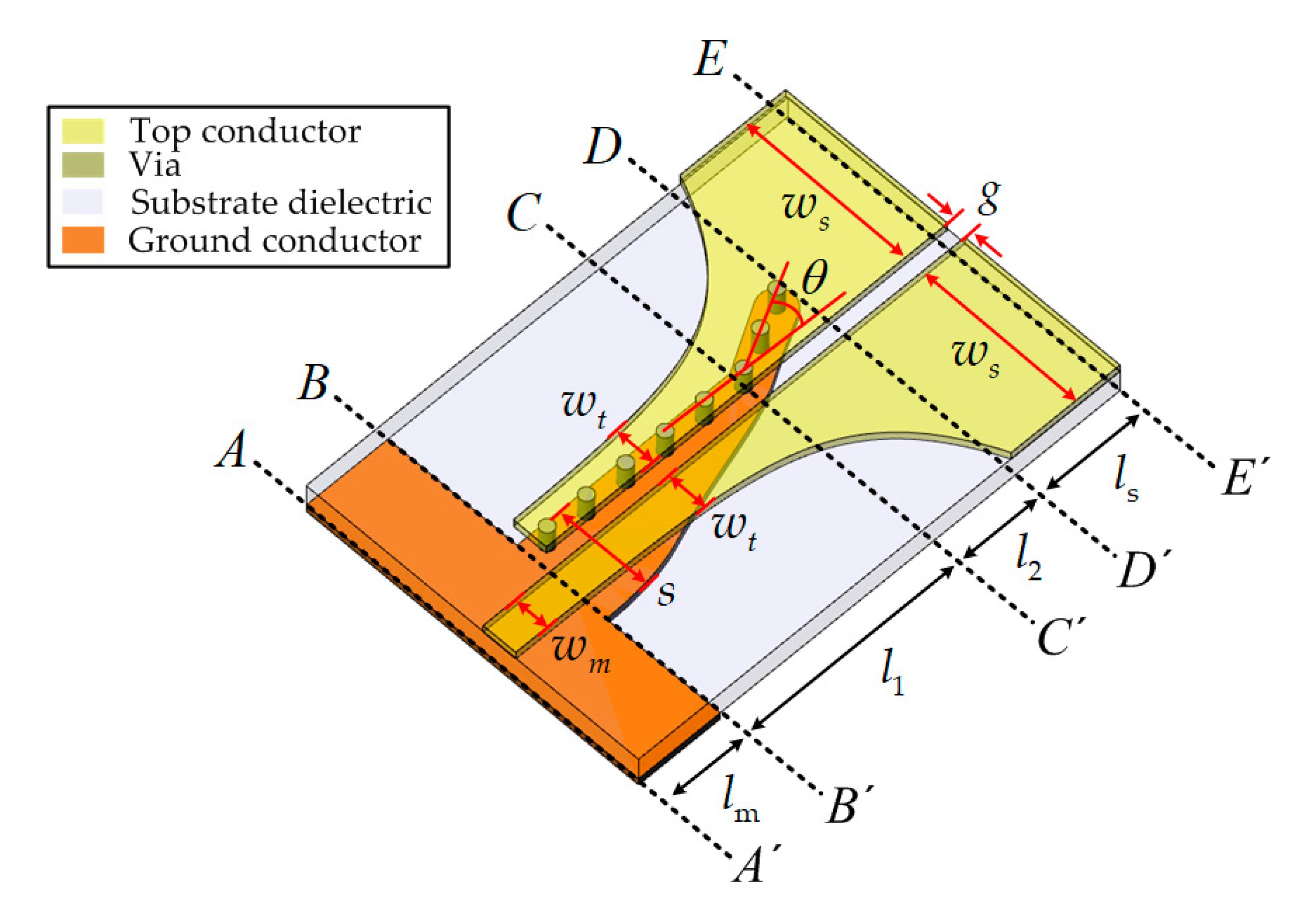
The proposed microstrip-to-slotline transition is illustrated in Figure 1. For a systematic analysis, the transition can be divided into four sections. AA′-BB′ is a microstrip line section with width wm and length lm. In BB′-CC′, the microstrip line changes to a ground-backed coplanar stripline (CPS) structure, where the microstrip ground is connected to one line of the CPS with multiple vias. For the BB′-CC′ section, the line length is l1, the width of the ground strip (s) is decreased along the stretch of the transition. The microstrip signal line is connected to the slotline conductor, and the line width (wt) is exponentially increased to the width (ws) of the slotline conductor at DD′. The slot gap on the top substrate is maintained at g. At a short CC′-DD′ section of length l2, the narrow ground strip is bent at an angle (θ) while still having multiple vias to connect to the top conductor. DD′-EE′ is a typical slotline with gap width of g and length of ls.

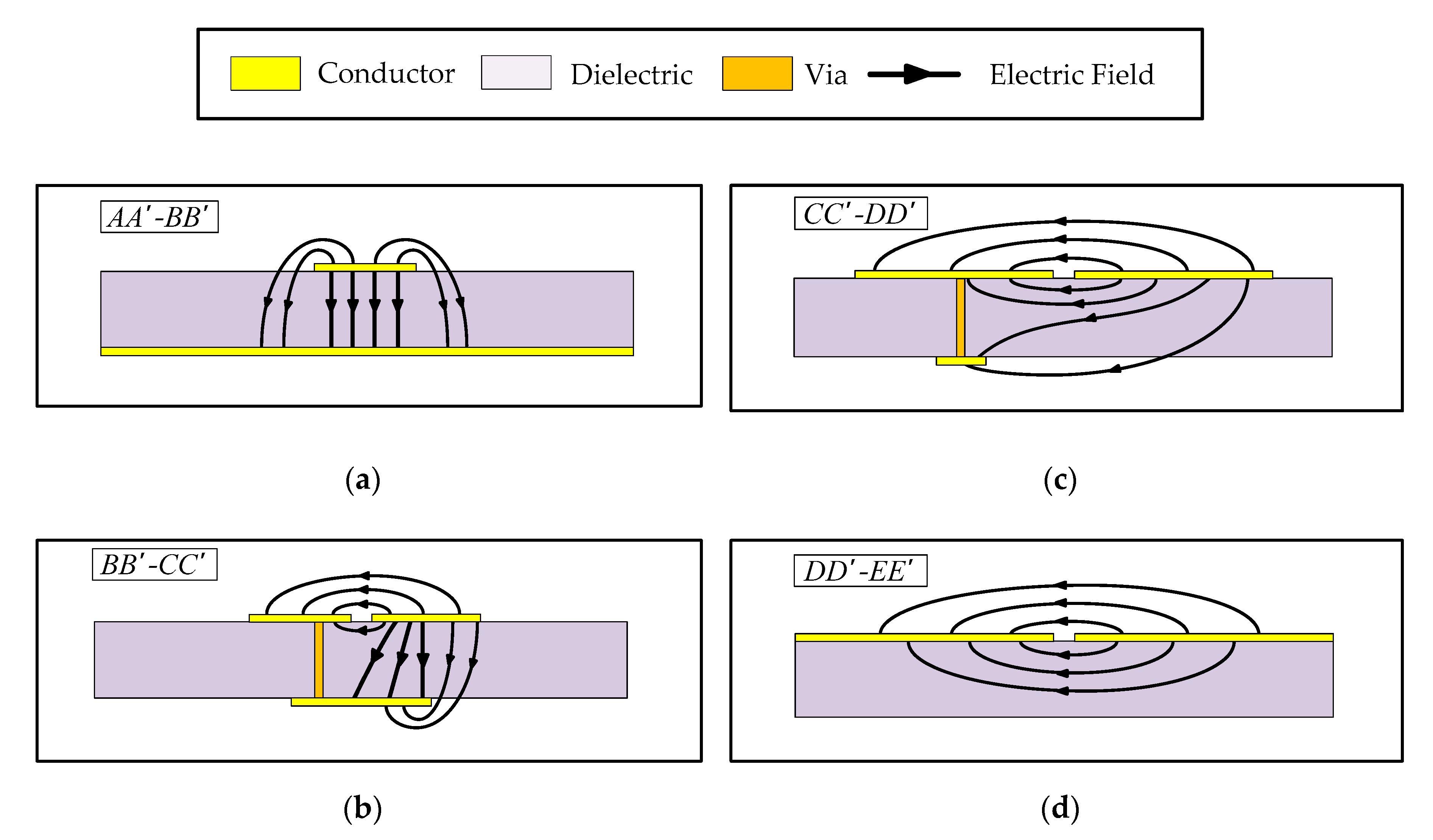
2.1. Electric Field Distributions

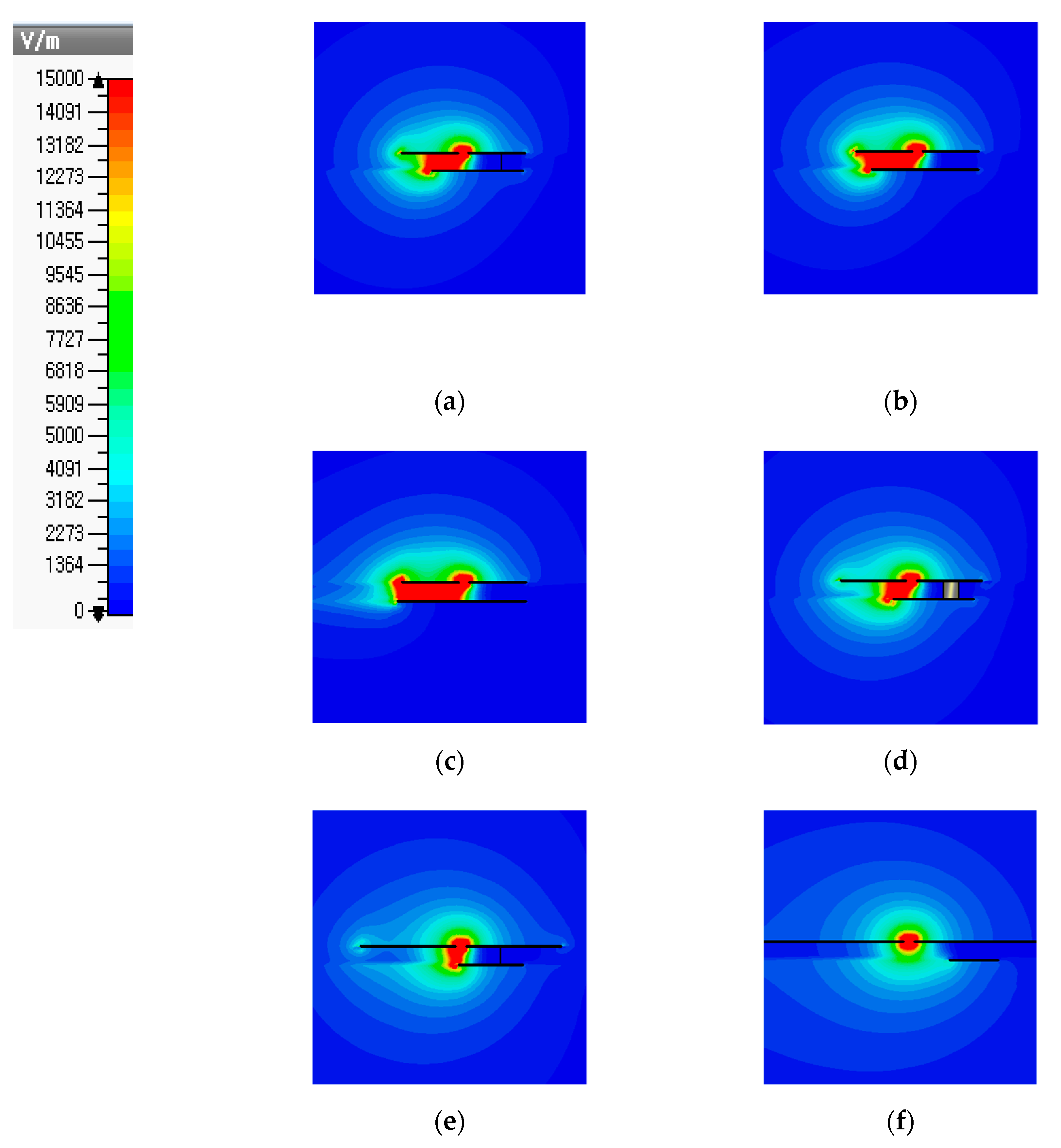
Cross-sectional electric field distributions at various stages of the transition are simplified and illustrated in Figure 2. At AA′-BB′, a typical quasi-TEM field distribution of a microstrip line, which is mostly vertical, is shown. The electric field distribution at the BB′-CC′ section consists of two contributions. First, there is a mostly horizontal CPS field distribution at the upper air region. Second, there exists a mostly vertical field distribution between the conductor strip extended from the microstrip signal line and the reduced ground strip, which is connected through multiple vias (via wall) to the upper ground line. These field lines are residing mostly inside the dielectric, but, as the ground linewidth on the bottom side further reduces, there occur some fringing field lines that pass through the dielectric region and hoop back to the bottom ground strip. At the short CC′-DD′ section, as the widths of the upper conductors are widened, the narrow bottom ground strip with vias is bent at an angle and the via locations are moved further away from the slot center to smoothly transform into the slotline field distribution. Because of the existence of the via-ed ground strip, the field inside the dielectric can be modelled as a quasi-TEM-like distribution, and finally becomes a quasi-TE field distribution of the slotline at EE′. The slotline, with wide-width conductors separated by a slot gap, has horizontally dominated field distributions similar to the CPS line, but it has almost TE mode signal with a small longitudinal magnetic component. In principle, the conformal mapping method applies only to the structures supporting quasi-TEM modes, but, in our proposed microstrip-to-slotline transition, the quasi-TEM-dominated transitional structure is retained up to a very close location to the start of slotline, enabling application of the conformal mapping in the design of the microstrip-to-slotline transition.

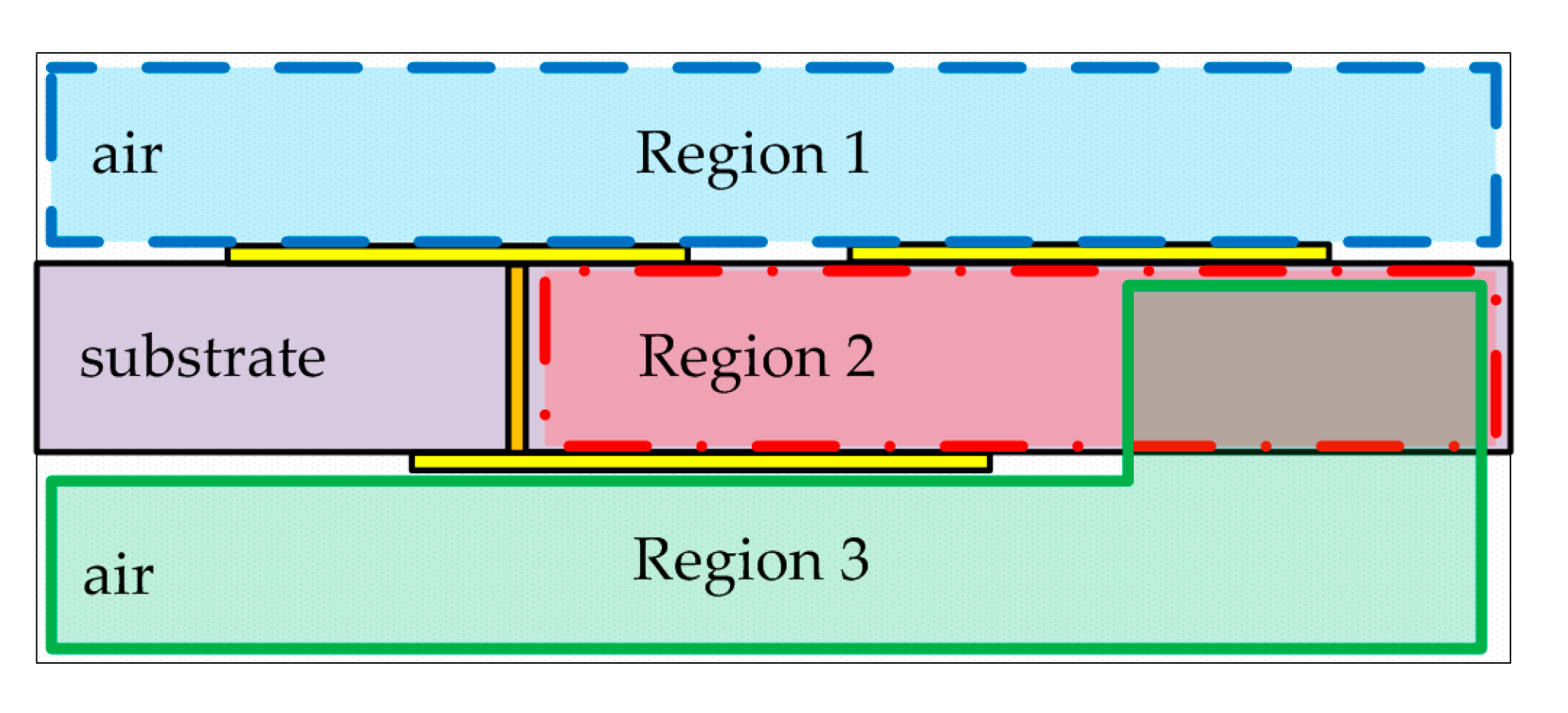
2.2. Transition Modeling for Transition Cross-Sections

Figure 3 illustrates a cross-section of the proposed transition. In order to analyze the transition based on the Schwarz-Christoffel transformation (one of conformal mapping methods), the cross-section is divided into three regions. Region 1 represents the field formation in the air because of the top-side conductors of the substrate. Region 2 covers the distributed fields inside the substrate, and Region 3 addresses the fringing field components, which pass through the substrate dielectric and hoop back to the bottom ground conductor from the bottom air portion. In the proposed cross-sectional analysis model, assuming a perfect electric wall at the via center positions, the small field contribution in the region on the other side of via is ignored.
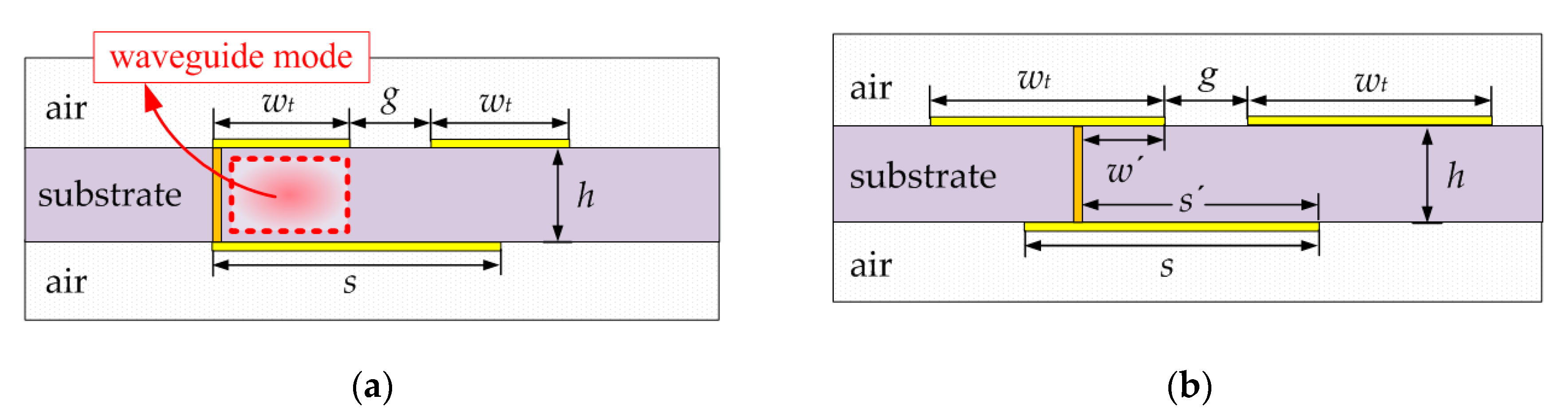
In a previous microstrip-to-CPS transition implementation, the via locations were fixed with w′ = wt, s′ = s as illustrated in Figure 4a [15]. To analyze the proposed microstrip-to-slotline transition, the via location is modified. The conductor width of the slot line is much wider than that of CPS, and the inside region wrapped by wide ground strips and vias can support a spurious half-wave SIW (substrate integrated waveguide) mode, causing increased insertion loss at specific frequencies. In addition, with wider conductor widths (i.e., in slotline), the analysis Regions 1 and 2 do not support the quasi-TEM mode, and the conformal mapping cannot be applied. Therefore, in the suggested model shown in Figure 4b, the vias are placed close to the slot. The transition model for Region 2 is modified by considering the electric field contribution due to the shorted conductor strip w′, via, and the ground conductor strip s′. If w′ is sufficiently small, most of the field lines are concentrated in Region 2 supporting the quasi-TEM mode, and the conformal mapping can be applied to obtain the line capacitance. Therefore, the transition model for the Regions 1 and 3 are same as the previous microstrip-to-CPS transition [15].
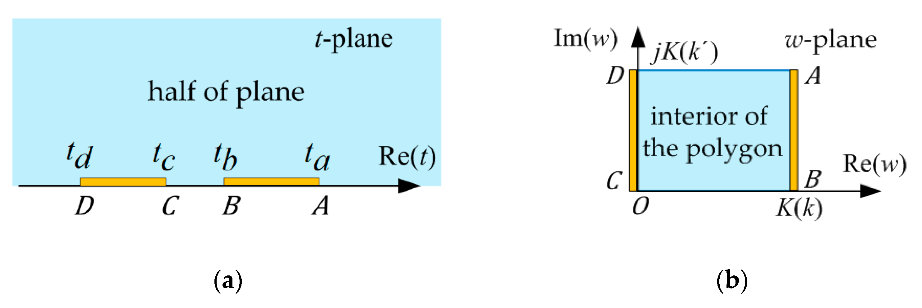
Using conformal mapping, the planar transitional structure can be transformed into a simple parallel capacitor in order to obtain the line capacitance and line impedance of the transition [16]. The field distributions of the transitional structure are assumed to be in quasi-TEM mode. The capacitance between two lines with four mapping points located at the horizontal axis of the t-plane in Figure 5a can be obtain as the capacitance of a simple capacitor in the w-plane in Figure 5b using the Schwarz-Christoffel transformation. This mapping is expressed as the following relationship in (1).
w ( t ) = U [     ( t t a ) ( α π 1 ) ( t t b ) ( β π 1 ) ( t t c ) ( γ π 1 ) ( t t d ) ( δ π 1 ) d t ] + V
where U and V are complex constants, and α, β, γ, and δ are the interior angles (all π/2, respectively) of the polygonal area at points A, B, C, and D of the w-plane. Assume that U is a normalizing constant and V is zero at boundary points. The width and height of a rectangle in the w-plane can be expressed as a form of the complete elliptic integrals of the first kind as given in (2) and (3). In this process, we use the elliptic integral theorem for arbitrary 4 points ( t a > t b > t c > t d ) on the horizontal axis [17].
A B ¯ = w ( t a ) w ( t b ) = t b t a d t ( t t a ) ( t t b ) ( t t c ) ( t t d ) = j K ( k )
B C ¯ = w ( t b ) w ( t c ) = t c t b d t ( t t a ) ( t t b ) ( t t c ) ( t t d ) = K ( k )
where K ( k ) and K ( k ) are the complete elliptic integrals, and their modulus k and k are expressed as (4) [17].
k = ( t b t c ) ( t a t d ) ( t a t c ) ( t b t d ) = 1 k 2
Region 1:
Region 1 can be regarded as part of a CPS structure having the line width of wt and the slot gap of g. Boundary points of the conductor are located as (5).
t a   = g / 2 +   w t   ,   t b   =   g / 2   ,   t c   =   g / 2 ,   t d   = g / 2 w t
Then the capacitance of Region 1 can be expressed by (6) by applying (1)–(3).
C 1 = ε 0 A B ¯ B C ¯ = ε 0 K ( k 1 ) K ( k 1 )
where modulus k 1 and k 1 of the complete elliptic integral can be obtained by using (4) and (5).
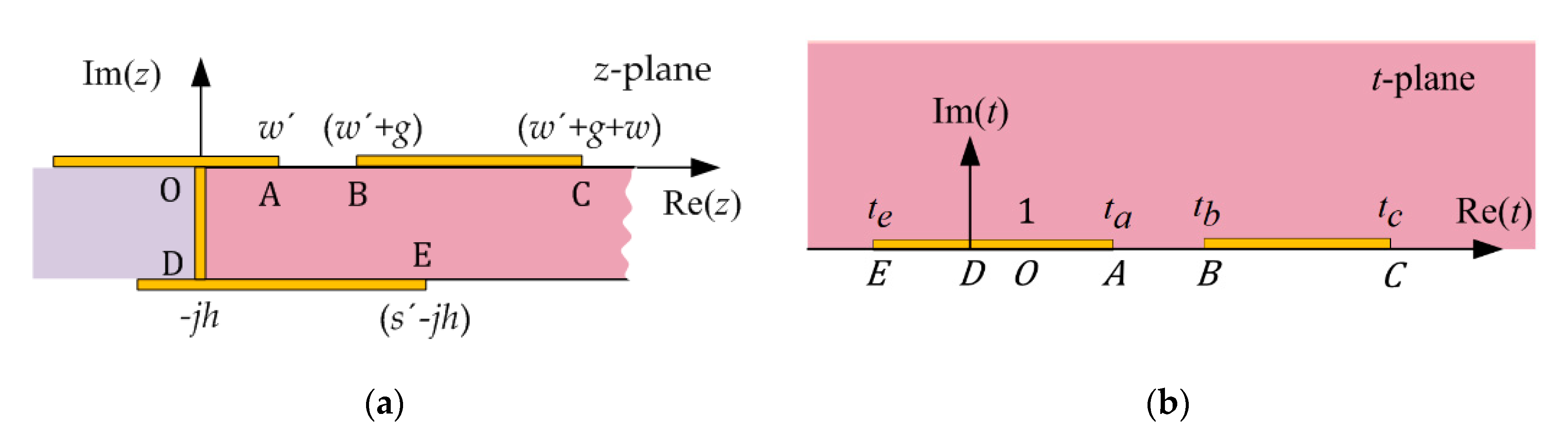
k 1 = g   ( g   +   2 w t ) ( g   +   w t ) 2 = 1 k 1 2
Region 2:
Region 2 is the internal space of the substrate dielectric as shown in Figure 6a. With the boundary conditions in Table 1, the points in the z-plane are mapped onto the t-plane points as shown in Figure 6 by applying the Schwarz-Christoffel transformation in (8).
z ( t ) = U 0 t d t t ( t 1 ) + V
where U and V are complex constants.
Let’s put t = cos h 2 θ , and d t = ( 2 sin h θ   cos h θ   ) d θ into (8). Then, we have
z ( t ) = U j π 2 θ   ( 2 sin h θ cos h θ ) d θ cosh 2 θ ( cosh 2 θ 1 ) + V = U j π 2 θ   2 d θ + V
From mapped points in Table 1, we have
z ( 0 ) = V = j h
z ( 1 ) = U j π 2 j π   2 d θ j h = 0         U = h π
Therefore, the inverse function of (9) is expressed as (12).
  t = cosh 2 ( π 2 h z + j π ) = cosh 2 ( π 2 h z )
The mapped points of A, B, C, and E can be expressed as (13) on the real-axis in the t-plane.
t a   = cosh 2 ( π w / 2 h )   ,   t b   =   cosh 2 ( π ( w + g ) / 2 h )   , t c   =   cosh 2 ( π ( w + g + w t ) / 2 h )   , t e   = sinh 2 ( π s / 2 h )
Then, these four points can be applied to the conformal mapping of Figure 5, and the capacitance C2 with modulus k 2 and k 2 of Region 2 can be expressed by (14) and (15) through applying (1)–(3).
C 2 = ε 0 ε r K ( k 2 ) K ( k 2 )
where ε r is the relative dielectric constant of substrate.
k 2 = ( t b t a ) ( t c t e ) ( t c t a ) ( t b t e ) = 1 k 2 2
Region 3:
Region 3 represents fringing fields formed between the signal line on the top of substrate and the bottom ground plane. By applying the conformal mapping to the entire structure, ignoring the permittivity, the electric field line from point C reaches point B [18]. For the analysis of the electric fields in Region 3, the virtual signal line width w″ can be determined with dependency of the width of the ground plane and the thickness of the substrate as given in (16) and (17).
g = { h π ,             for   w + g < s + h π w + g s ,                 elsewhere
w = { w + g + w t s h π ,             for   w + g < s + h π w t ,                             elsewhere
With the boundary conditions in Table 2, the points in the z-plane are mapped onto the t-plane points as shown in Figure 7 by applying the Schwarz-Christoffel transformation in (18).
z ( t ) = U [     ( t 1 ) ( α π 1 ) ( t + 1 ) ( β π 1 ) d t ] + V         = U [ t + 1 t 1 2 sinh 1 ( t 1 2 ) ] + V
where U and V are complex constants, and α and β are the interior angles (π/2 and 3π/2, respectively) of the polygonal area at points B and O of the z-plane. From the mapped points in Table 2, we have
z ( 1 ) = V = 0
z ( 1 ) = U ( j π ) = j h         U = h π
Therefore,
z ( t ) = h π [ t + 1 t 1 2 sinh 1 ( t 1 2 ) ]
The capacitance C3 with modulus k 3 and k 3 of Region 3 are expressed as (22) and (23), similarly to Region 2.
  C 3 = ε 0 K ( k 3 ) K ( k 3 )
k 3 = ( t c + 1 ) ( t d t a ) ( t d + 1 ) ( t c t a )   = 1 k 3 2  
where the real points t a , t b (= 1), t c and t d of the t-plane can be obtained by substituting the complex values of points A, C, and D in the z-plane into (21). Therefore, the characteristic line impedance Z0 can be obtained by combining capacitances from three regions ( C 1 ,   C 2 ,   C 3 ) and the relative dielectric constant of the substrate [15].
Z 0 = 120 π ε eff   ( C 1 + C 2 / ε r + C 3 ) / ε 0
where the effective permittivity ε eff is defined as
ε eff   = ( C 1 + C 2 + C 3 ) ( C 1 + C 2 / ε r + C 3 )

2.3. Design of the Microstrip-to-Slotline Transition

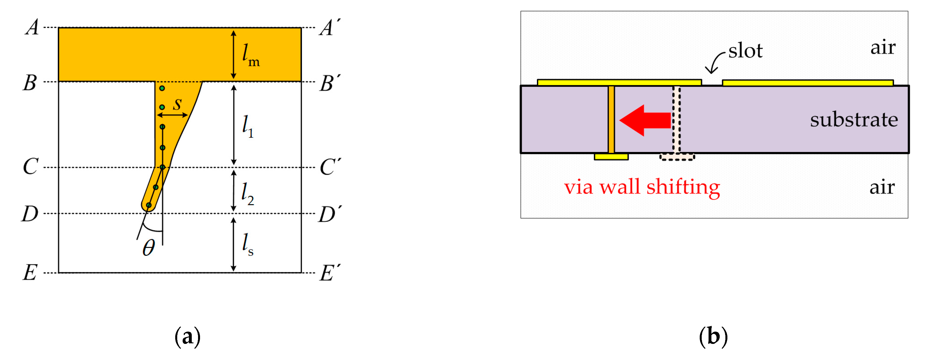
For the design of the proposed microstrip-to-slotline transition, the Rogers Duroid 5880 substrate with a thickness of 10 mil and a relative dielectric constant of 2.2 is used. Typically, high-dielectric substrates are used to implement the microstrip-to-slotline transition in order to prevent the resonating parasitic modes between stubs. In this paper, the proposed transition is composed of a continuous signal line without stubs and can be implemented on low dielectric constant substrates.
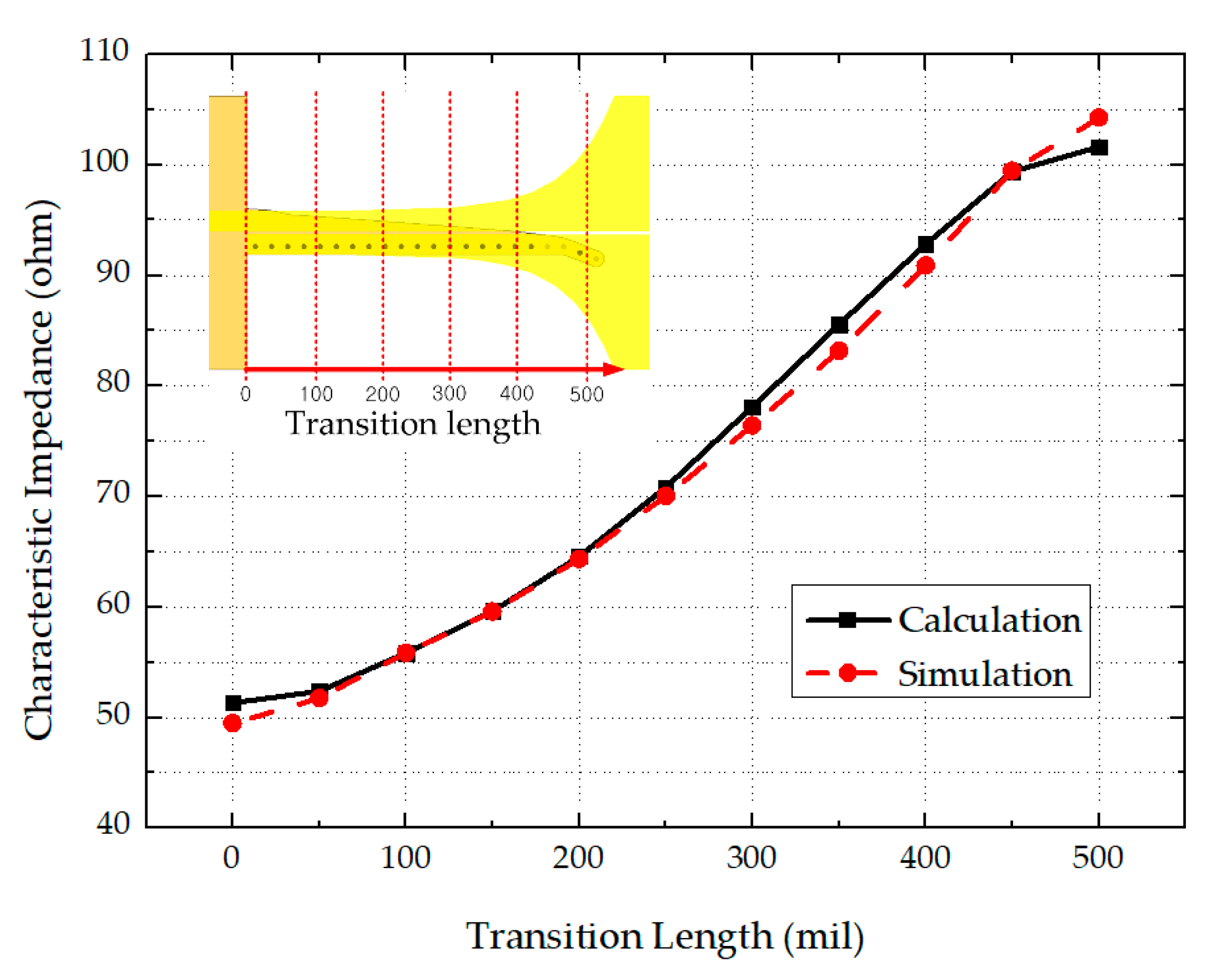
To design the proposed transition, the characteristic line impedance of the cross-section at any point of the proposed transition can be calculated using the analytical formula given in (24). To obtain ultra-wide bandwidth with the proposed transition, the line impedance from the microstrip, through the transition structure, and to the slotline should be optimally matched. In the proposed transition, the microstrip impedance is 50 Ω, and the slotline impedance is selected as 100 Ω. In the proposed transition design, the line impedance from microstrip to slotline is optimally tapered using the Klopfenstein impedance taper. With the Klopfenstein impedance taper, the target impedance value as a function of length can be determined. Then, the design parameters of the transition can be adjusted to attain the target impedance. For the transitional section (BB′-DD′), the widths of the upper two conductors of the CPS line are exponentially flared, while the bottom ground width s is determined to satisfy the Klopfenstein tapering. In BB′-CC′, the via wall is formed linearly at w′ = 18 mil, and the width of the ground strip reduces from 67.8 mil at BB′ to 24.5 mil at 
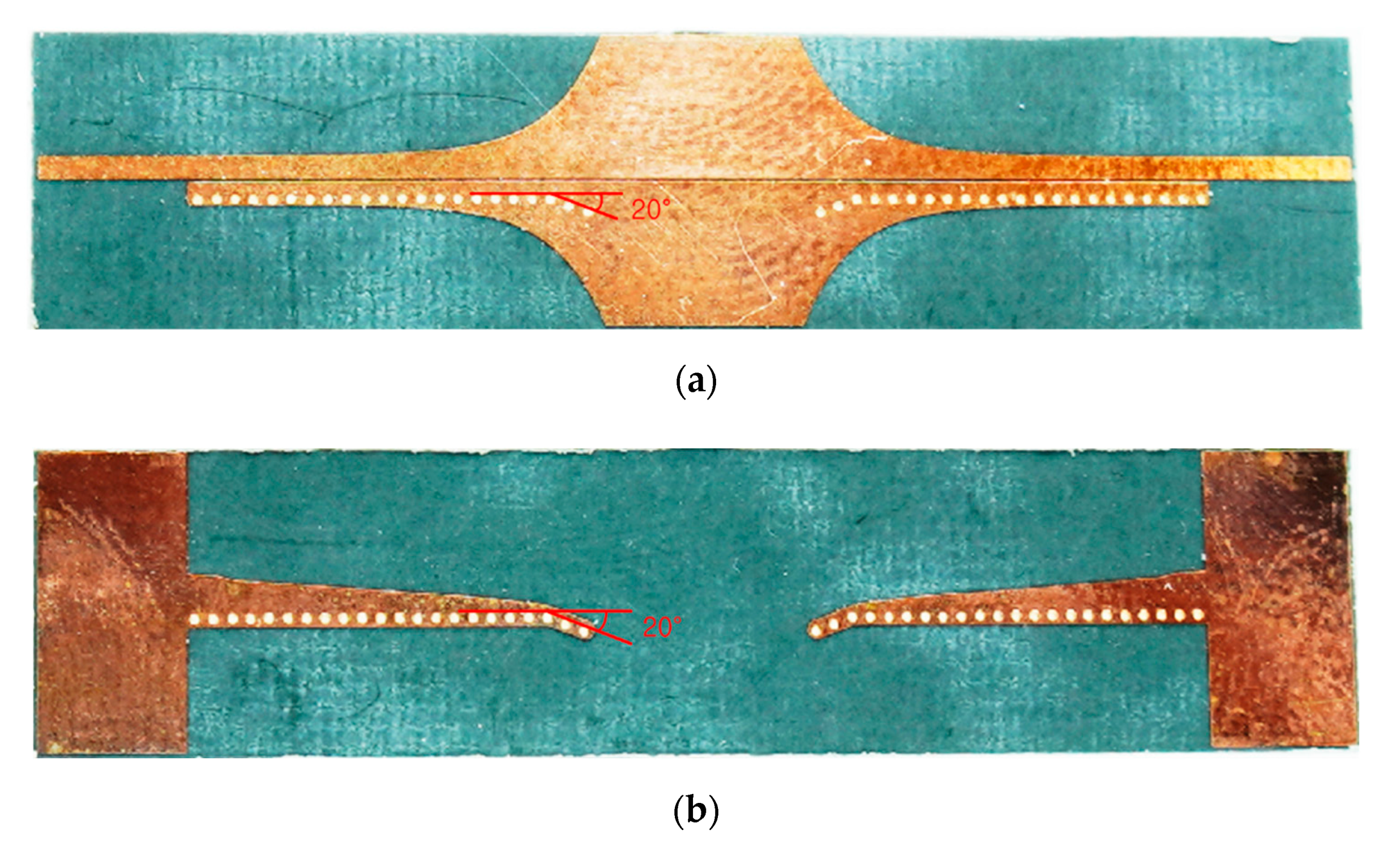
CC′ to satisfy the Klopfenstein impedance taper. In order to obtain a higher line impedance, the width of the ground strip should be further reduced, but then the conductor strip cannot accommodate the via holes. Instead, at the CC´-DD´ section, the ground strip is bent at an angle of θ as shown in Figure 8a, so that the ground strip maintains a width of 24 mil. By bending this ground strip, the via wall is also moved further away from the slot as shown in Figure 8b, helping smooth transformation of the field lines to those of slotline as well as satisfying the Klopfenstein impedance taper.
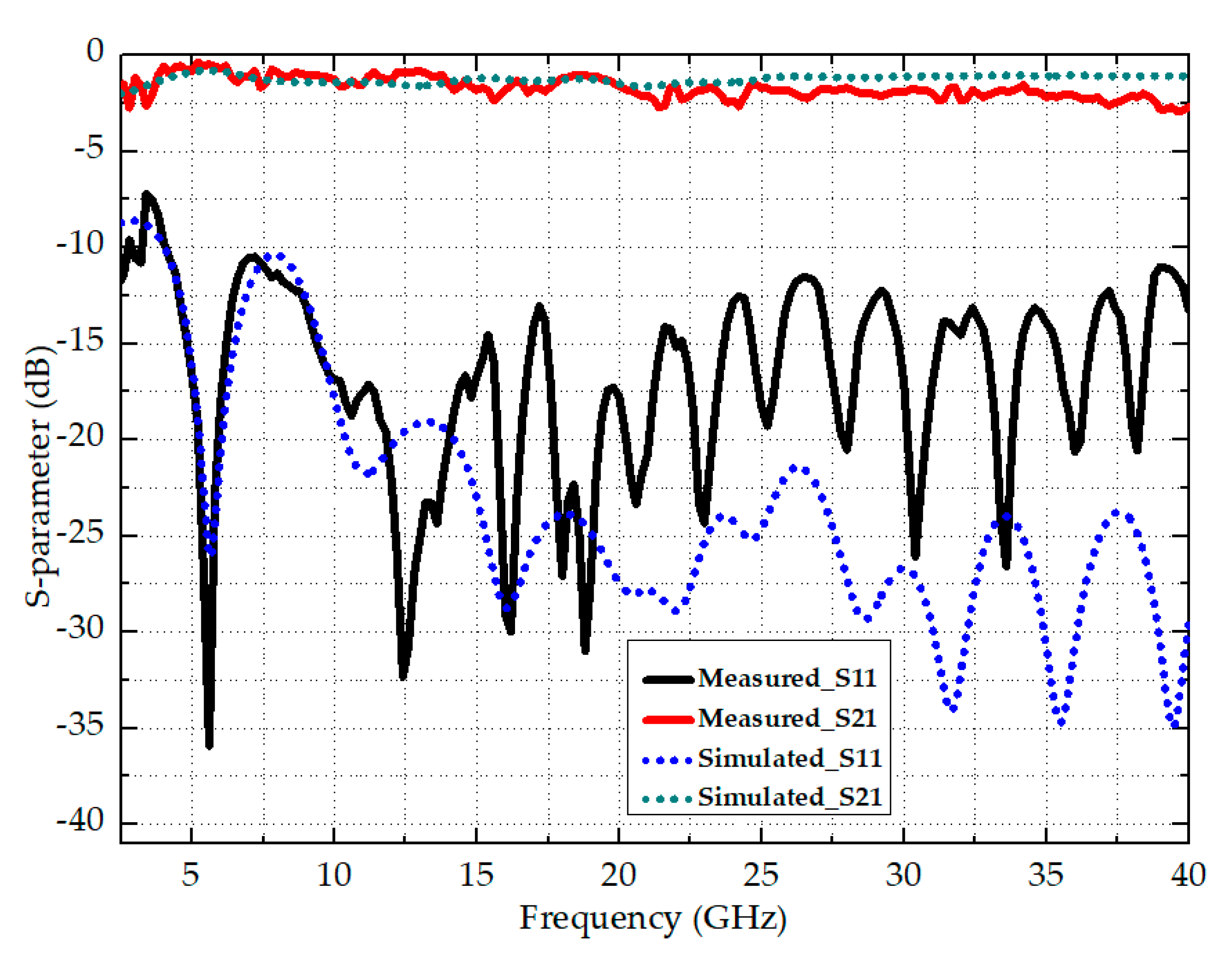
With impedance tapering, the transition length determines the lowest operating frequency; i.e., with longer transition length, the minimum operating frequency becomes lower. In addition to the impedance matching, the transition should smoothly transform electric field lines from the microstrip line to the slotline without abrupt shape changes.

3. Simulation and Measurements

The proposed microstrip-to-slotline transition is fabricated in a back-to-back configuration with size of 1735.8 mil × 405 mil × 11.4 mil as shown in Figure 9. The vias with diameter of 8 mil are arrayed by 24-mil spacing. The design parameters of the proposed transition are shown in Table 3. The bent angle of the ground strip is chosen as θ = 20° in order to satisfy the Klopfenstein impedance taper.

3.1. Simulation

To verify the proposed transition design based on the analytical formula, a commercial 3D EM simulator (CST Microwave Studio) is used to obtain characteristic line impedance, electric field distributions at various cross-sectional stages, and S-parameters. The calculated and simulated line impedance along the stretch of the proposed transition is shown in Figure 10. The difference is within 3% in the BB′-CC′ section (0 to 468 mil), and increases slightly in the CC′-DD′ section (468 mil to 543 mil). In obtaining the proposed analytical formulas, the conductor thickness is neglected, but in the EM simulation copper thickness of 0.669 mil is included. From the region close to the slot line, the quasi-TEM mode signal changes to the quasi-TE mode signal, and the accuracy of the proposed analysis model is slightly degraded in the CC′-DD′ section. With the proposed analytical model, however, the impedance difference is less than 3 Ω, and the implementation of the proposed ultra-wideband transition can be designed with the analytical formulas without a time-consuming parameter tuning process.
The electric field distributions at several cross-sections by a 100 mil interval along the transition are shown in Figure 11. For the cross-sectional regions where wide width of the ground plane is present, the field lines are distributed mostly inside the dielectric as shown in Figure 11a–e, thus validating the assumption of the quasi-TEM mode. In Figure 11f, the field is mostly concentrated at the slot gap between the two wide conductors, consisting of mixed TEM and TE modes.

3.2. Measurements

The fabricated microstrip-to-slotline transition in the back-to-back configuration (Figure 9) is measured with the Anritsu universal test fixture and MS4644B vector network analyzer. The measured and simulated insertion loss (|S21|) and return loss (|S11|) are shown in Figure 12. The proposed transition exhibits insertion loss less than 2.9 dB (1.5 dB per transition) and return loss more than 10 dB from 4.4 GHz to 40 GHz. The performance tends to degrade at higher frequencies, possibly due to fabrication tolerances, substrate loss tangent, and the test fixture to mount the proposed transition. The performance comparison with previously reported designs is listed in Table 4.
As compared with the reported results in the open literature, the proposed transition designed in a low dielectric constant substrate possesses much wider performance bandwidth than the transitions with cross-junctions with stubs, and higher operation frequency than the ground coupling transition having a continuous signal line without via. In addition, if the proposed transition is designed with a high dielectric constant substrate, the transition can perform better because the electric field lines can be concentrated inside the dielectric and approach the TEM mode.

4. Conclusions

The proposed ultra-wideband microstrip-to-slotline transition is designed and implemented by applying optimal impedance matching and smooth field transformation using an analytical line impedance formula based on conformal mapping. Even though the slotline supports non-TEM mode signals, the parallel ground strip with the via wall helps to retain most of field lines inside the dielectric substrate, thus permitting the use of the quasi-TEM-based conformal mapping for this transition design. The calculated characteristic line impedances enable to directly design an optimal impedance taper through the stretch of the transition without a time-consuming parameter tuning process using EM simulators. Also, the proposed transition design demonstrates ultra-wideband performance even with a low permittivity substrate, providing flexibility in integrating with various microwave circuit boards and antennas.

Author Contributions

Conceptualization, J.S.L., G.H.L., H.C.C., and K.W.K.; methodology, J.S.L. and G.H.L.; software, J.S.L.; validation, J.S.L., G.H.L., H.C.C., and K.W.K.; formal analysis, J.S.L., G.H.L., W.M., H.C.C., and K.W.K.; investigation, J.S.L., G.H.L., H.C.C., and K.W.K.; resources, J.S.L., G.H.L., H.C.C., and K.W.K.; data curation, J.S.L., G.H.L., W.M., H.C.C., and K.W.K.; writing—original draft preparation, J.S.L. and G.H.L.; writing—review and editing, J.S.L., G.H.L., W.M., H.C.C., and K.W.K.; visualization, J.S.L.; supervision, H.C.C. and K.W.K.; project administration, H.C.C. and K.W.K.; funding acquisition, H.C.C. and K.W.K. All authors have read and agreed to the published version of the manuscript.

Funding

This research was supported by the National R&D Program through the National Research Foundation of Korea (NRF) funded by the Ministry of Education, Science and Technology [NRF-2019M1A7A1A02085630] and the BK21 Plus Project funded by the Ministry of Education, Korea [No. 21A20131600011].

Conflicts of Interest

The authors declare no conflict of interest.

References

  1. Edwards, T.C.; Steer, M.B. Foundations for Microstrip Circuit Design, 4th ed.; Wiley: West Sussex, UK, 2016; pp. 443–464. [Google Scholar]
  2. Gupta, K.C.; Garg, R.; Bahl, I.J.; Bhartia, P. Microstrip Lines and Slotlines, 3rd ed.; Artech House: Boston, MA, USA, 1996; pp. 239–297. [Google Scholar]
  3. Cohn, S.B. Slot line on a dielectric substrate. IEEE Trans. Microw. Theory Tech. 1969, 17, 768–778. [Google Scholar] [CrossRef]
  4. Shuppert, B. Microstrip/slotline transitions: Modeling and experimental investigation. IEEE Trans. Microw. Theory Tech. 1988, 36, 1272–1282. [Google Scholar] [CrossRef]
  5. U-yen, K.; Wollack, E.J. Slotline Stepped Circular Rings for Low-Loss Microstrip-to-Slotline Transitions. Microw. Wirel. Compon. Lett. IEEE 2007, 17, 100–102. [Google Scholar] [CrossRef]
  6. Akhavan, H.G.; Mirshekar-Syahkal, D. Analysis of broadband microstrip-slotline transitions with multi-arm stubs. Electron. Lett. 1996, 32, 2106–2108. [Google Scholar] [CrossRef]
  7. Schiek, B.; Kohler, J. An improved microstrip-to-microstrip transition. IEEE Trans. Microw. Theory Tech. 1976, MTT-24, 231–233. [Google Scholar] [CrossRef]
  8. Guo, X.; Zhu, L.; Wang, J.; Wu, W. Wideband microstrip-to-microstrip vertical transitions via multiresonant modes in a slotline resonator. IEEE Trans. Microw. Theory Tech. 2015, 63, 1902–1909. [Google Scholar] [CrossRef]
  9. Nasr, A.M.H.; Safwat, A.M.E.; Elhennawy, H. Via-free microstrip to slotline Baluns using slotted microstrip cross-junction. In Proceedings of the 2017 47th European Microwave Conference (EuMC 2017), Nuremberg, Germany, 21 December 2017; pp. 85–88. [Google Scholar]
  10. Ta, S.X.; Han, J.J.; Choo, H.; Park, I. High gain 60 GHz band printed quasi-Yagi antenna using a novel microstrip-slotline transition feed. In Proceedings of the 5th Global Symposium on Millimeter-Waves, Harbin, China, 27 September 2012; pp. 1–4. [Google Scholar]
  11. Dib, N.I.; Simons, R.N.; Katehi, L.P.B. Broadband uniplanar microstrip to slot-line transitions. In Proceedings of the 1995 IEEE MTT-S International Microwave Symposium, Orlando, FL, USA, 16–20 May 1995; pp. 683–686. [Google Scholar]
  12. Li, J.L.; Shao, W.; Yang, X.S. An ultra-wideband microstrip-to-slotline transition. J. Electromagn. Waves Appl. 2012, 26, 1889–1896. [Google Scholar] [CrossRef]
  13. Tu, W.H.; Chang, K. Wide-band microstrip-to-coplanar stripline/ slotline transitions. IEEE Trans. Microw. Theory Tech. 2006, 54, 1084–1089. [Google Scholar]
  14. Fei, P.; Jiao, Y.C.; Zhang, Z.; Hu, W.; Zhang, F.S. Compact coupled line broadband microstrip to slotline transition. Electron. Lett. 2011, 47, 751–752. [Google Scholar] [CrossRef]
  15. Lee, G.H.; Mohyuddin, W.; Choi, H.C.; Kim, K.W. Asymmetric ultra-wideband microstrip-to-coplanar stripline transition. IEEE Microw. Wirel. Compon. Lett. 2018, 28, 386–388. [Google Scholar]
  16. Schinzinger, R.; Laura, P.A.A. Conformal Mapping: Methods and Applications; Dover Publications: New York, NY, USA, 2003; pp. 266–319. [Google Scholar]
  17. Hancock, H. Elliptic Integral; John Willey&Sons Inc.: New York, NY, USA, 1917; pp. 47–48. [Google Scholar]
  18. Pesonen, N.; Kahn, K. Application of conformal mapping approximation Techniques: Parallel conductors of finite dimensions. IEEE Trans. Microw. Theory Tech. 2004, MTT-53, 812–817. [Google Scholar] [CrossRef]
Figure 1. Proposed microstrip-to-slotline transition configuration.
Electronics 09 01329 g001
Figure 2. Electric field distribution at each section of the proposed transition: (a) AA′-BB′; (b) BB′-CC′; (c) CC′-DD′; (d) DD′-EE′.
Electronics 09 01329 g002
Figure 3. Three-regions of a cross-section of the proposed microstrip-to-slotline transition.
Electronics 09 01329 g003
Figure 4. Cross-sectional analysis model: (a) the microstrip-to- coplanar stripline (CPS) transition [15]; (b) the proposed microstrip-to-slotline transition.
Electronics 09 01329 g004
Figure 5. Mapping a rectangle in the w-plane onto arbitrary four points on the horizontal axis in the t-plane: (a) t-plane, (b) w-plane.
Electronics 09 01329 g005
Figure 6. Conformal mapping of Region 2: (a) z-plane, (b) t-plane.
Electronics 09 01329 g006
Figure 7. Conformal mapping of Region 3: (a) z-plane, (b) t-plane.
Electronics 09 01329 g007
Figure 8. Via wall shifting in the CC′-DD′ section: (a) bottom view; (b) side view.
Electronics 09 01329 g008
Figure 9. Fabricated microstrip-to-slotline transition: (a) top view; (b) bottom view.
Electronics 09 01329 g009
Figure 10. Characteristic line impedance along the transition length.
Electronics 09 01329 g010
Figure 11. Electric field distributions along the proposed transition: (a) 0 mil; (b) 100 mil; (c) 200 mil; (d) 300 mil; (e) 400 mil; (f) 500 mil position from the microstrip line.
Electronics 09 01329 g011
Figure 12. Results of the measured and simulated S-parameters.
Electronics 09 01329 g012
Table 1. Mapped points between the z-plane and t-plane in Region 2.
Symbolz-Planet-Plane
O01
Djh0
Table 2. Mapped points between the z-plane and t-plane in Region 3.
Symbolz-Planet-Plane
O01
Bjh−1
Table 3. Dimensions of the proposed transition (unit: mil).
wmwsglml1l2l3
30200520046875125
Table 4. Performance comparison of the proposed microstrip-to-slotline transition with the reported designs.
Refs.Frequency Range 1 (GHz)Min./Max. IL per Transition (dB)Relative Bandwidth 2 (%)Relative PermittivityTransition Type
[5]3–160.3/1.5136.82.9Cross Junction
[6]1–10---/1.5163.610.2Cross Junction
[7]2–9---/0.2127.310Cross junction
[8]2.46–11.00.2/1.4126.910.7Cross junction
[9]1.47–3.760.43/1.587.67Cross junction
[10]57–66---/1.014.62.2Cross junction
[11]7.5–10.50.3/1.533.310.5Phase shift
[12]1.1–16.51.2/1.5175.02.33Ground coupling
[13]2.7–10.4---/1.5117.62.33Ground coupling
[14]0.26–2.75---/1.5165.42.65Ground coupling
This work4.4–400.2/1.5160.42.2Tapering with vias
1 less than 3 dB back-to-back insertion loss (IL), and more than 10 dB return loss. 2 (Relative bandwidth) = (Frequency bandwidth)/(Center frequency).

