Article

A Ku-Band GaAs Multifunction Transmitter and Receiver Chipset

1
School of Electrical Engineering, Korea University, Anam-dong, Seongbuk-gu, Seoul 02841, Korea
2
Samsung Electronics, Samsungjeonja-ro, Hwasung-si, Gyeonggi-do 18448, Korea
3
Electronics and Communication Engineering, Republic of Korea Air Force Academy, P.O.Box 335-2, Danjae-ro, Namil-myeon, Sangdang-gu, Cheongju-si, Chungcheongbuk-do 28187, Korea
*
Author to whom correspondence should be addressed.
Electronics 2020, 9(8), 1327; https://doi.org/10.3390/electronics9081327
Submission received: 30 July 2020 / Revised: 10 August 2020 / Accepted: 11 August 2020 / Published: 17 August 2020
(This article belongs to the Section Microelectronics)

Abstract

:
This paper presents a Ku-band monolithic multifunction transmitter and receiver chipset fabricated in 0.25-μm GaAs pseudomorphic high-electron mobility transistor technology. The chipset achieves a high level of integration, including a 4-bit 360° digital phase shifter, 5-bit 15.5-dB digital attenuator, amplifier and 9-bit digital serial-to-parallel converter for digital circuit control. Since the multifunction chipset includes a medium power amplifier and a low-noise amplifier, it features high P1dB and low noise figures over the full Ku-band frequencies. The multifunction transmitter shows a peak gain of 16.5 dB with output P1dB of 19.2 dBm at 15 GHz. The multifunction receiver shows a peak gain of 17.3 dB with noise figure of 2.5 dB at 15 GHz. The attenuation range is 15.5 dB with a step of 0.5 dB and the phase shift range is 360° with a step of 22.5°. Each chip area of the transmitter and receiver is 4.2 × 2.8 mm2.

1. Introduction

Demand for phased-array systems has continued to increase for satellite/military communications and radars [1]. In the past, multiple individual modules were assembled to implement each channel element in the phased array, which increases the size, weight, complexity and cost of the system [2]. However, a multifunction chip integrates most of the functionalities required for the array element in a single chip, including the phase and amplitude control, signal amplification and digital control. This significantly reduces the system complexity and cost [3]. In particular, as the array size increases to a large scale, the benefit of the multifunction chip becomes more prominent. For this purpose, the chip should retain high integration level and compact size.
In recent years, several multifunction chips have been reported in GaAs or silicon technologies [1,4,5,6,7,8,9,10,11,12,13]. Silicon-based multifunction chips are favorable for their easy integration with digital circuits and low cost in the case of mass chip production [4]. However, GaAs technologies offer superior noise figures and output power over silicon technologies. In addition, digital circuits can be integrated even in GaAs technologies using a combination of enhancement-mode (E-mode) and depletion-mode (D-mode) transistors [14]. Therefore, it is more attractive to use GaAs technology for broadband multifunction chips with high gain, high output power and low noise figures. There are several articles which have reported on GaAs multifunction chips [1,8,9,10,11,12,13]. Nevertheless, many chips integrate only some, and not all, of the essential circuit blocks required for phased arrays, including a phase shifter, attenuator, amplifier and digital control circuit [1,8,9]. Other reports show narrowband operation [8,10] or relatively limited output power and high noise figures [11,13].
In this paper, a GaAs multifunction transmitter and receiver chipset operating over the full Ku-band (12–18 GHz) frequency is presented. A 4-bit digital phase shifter, 5-bit digital attenuator and 9-bit serial-to-parallel converter (SPC) are all integrated with a medium power amplifier (MPA) or a low-noise amplifier (LNA). This high integration level enables high output power and low noise figure and thus makes this chipset suitable for a large-scale phased-array system. This paper is organized as follows. In Section 2, the architecture of the multifunction transmitter and receiver are described. The design and measurement of each circuit building block are presented in Section 3. In Section 4, the measurement of the multifunction transmitter and receiver chipset is presented. The conclusion is presented in Section 5.

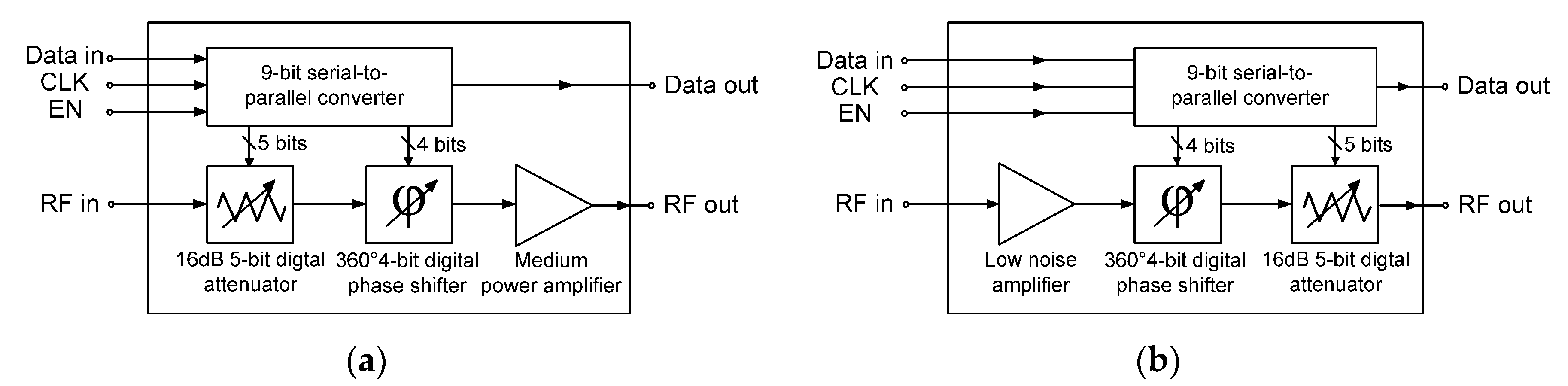
2. Ku-Band Multifunction Chip Architecture

The Ku-band multifunction chipset was designed using a commercial 0.25-μm GaAs pseudomorphic high-electron mobility transistor (pHEMT) technology. The process offers a 0.25-μm E-mode HEMT with fT = 75 GHz and a 0.5-μm D-mode HEMT with fT = 33 GHz. It also provides two metal layers, two types of capacitor (metal-insulator-metal capacitor and stack capacitor), three types of resistor (thin-film resistor, mesa resistor and epi resistor) and two types of inductor (spiral inductor and square inductor).
Figure 1 shows block diagrams of the Ku-band multifunction transmitter (a) and receiver (b). The multifunction transmitter consists of a 5-bit attenuator, 4-bit digital phase shifter, MPA and 9-bit SPC. The attenuator offers a total of 15.5 dB attenuation with a step of 0.5 dB. The phase shifter fulfills a 360° phase shift with a step of 22.5°. Both attenuator and phase shifter are digitally controlled by the SPC. The SPC converts a 9-bit serial digital code into a parallel code, which is loaded onto the attenuator and phase shifter for setting the desired attenuation and phase shift. This reduces the number of bonding pads for digital control. The attenuator is placed ahead of the phase shifter for broadband input matching. The MPA is placed in the final stage to enhance the output power and linearity of the transmitter.
The multifunction receiver is composed of an LNA, 4-bit digital phase shifter, 5-bit digital attenuator and 9-bit SPC. Similar to the transmitter, 15.5-dB attenuation and 360° phase shift are implemented in the receiver and are controlled by the SPC. The LNA is placed at the input stage for providing high gain and low noise figures.

3. Circuit Blocks of the Ku-Band Multifunction Chipset

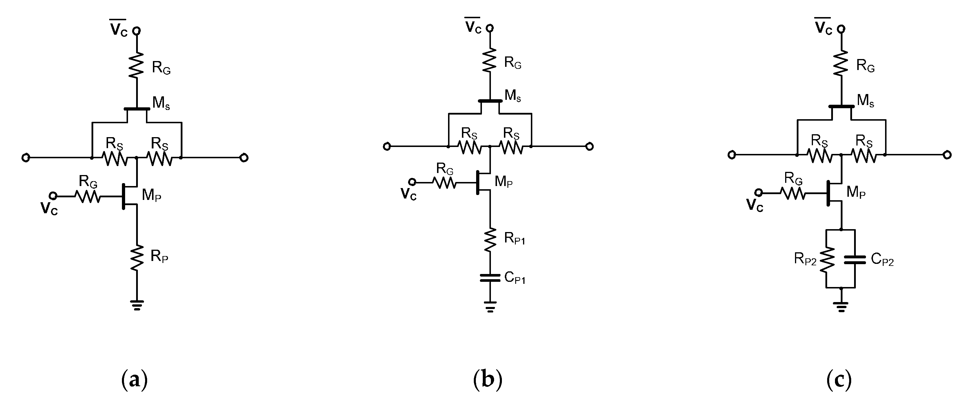
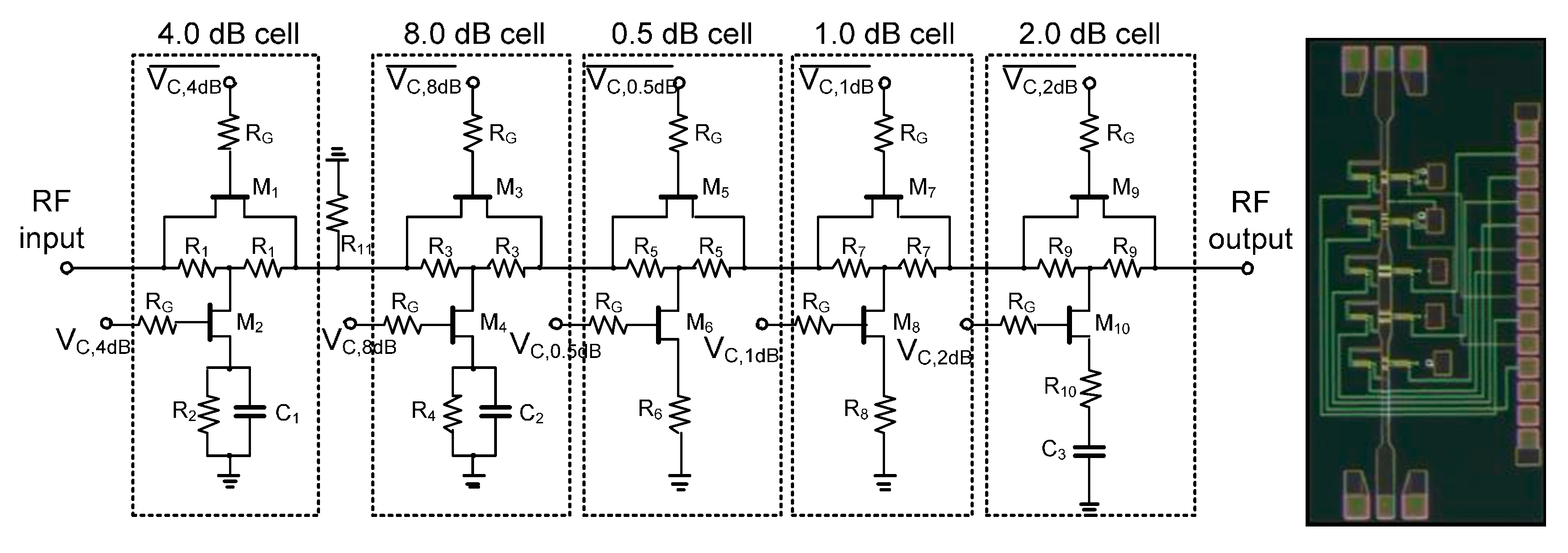
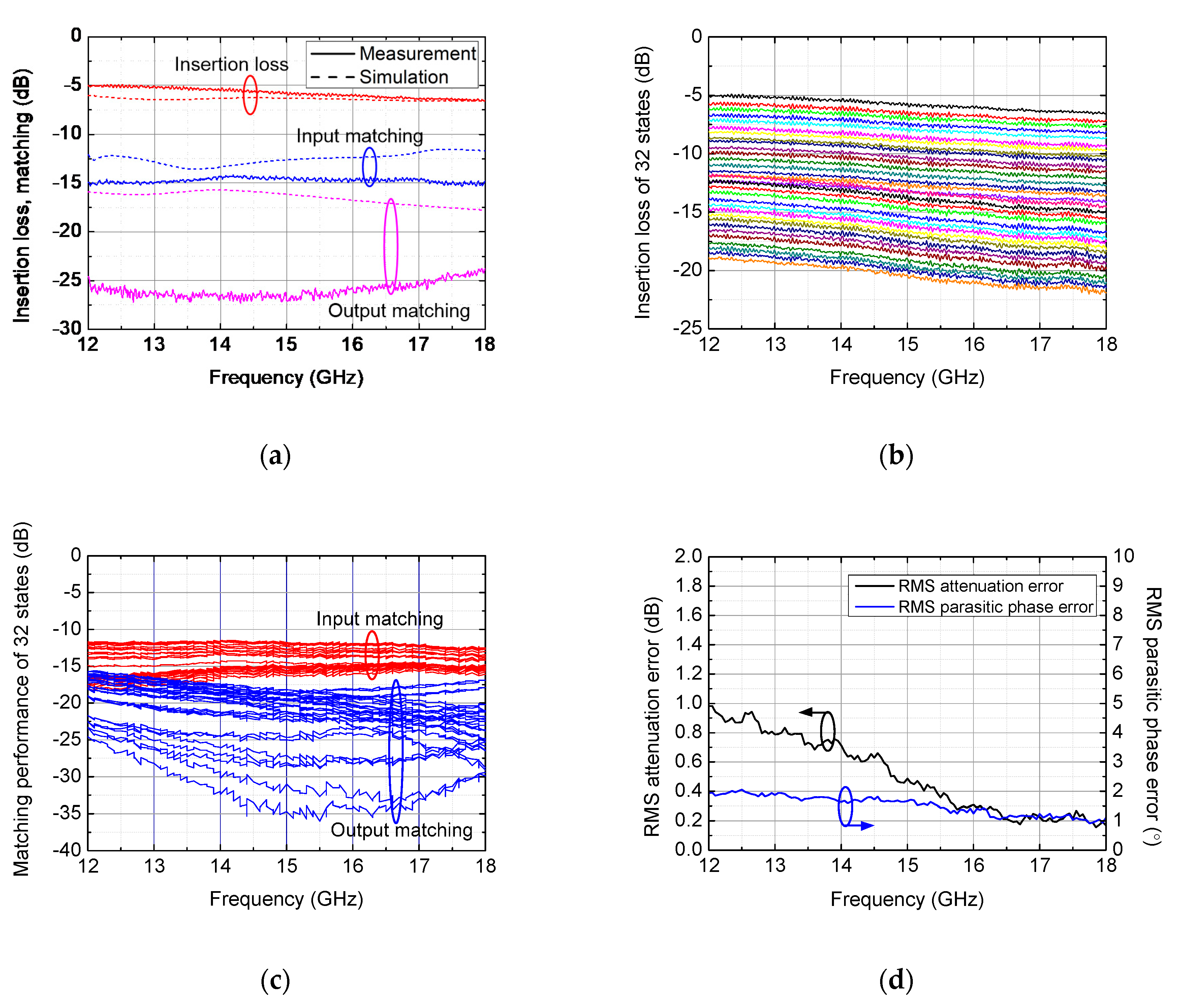
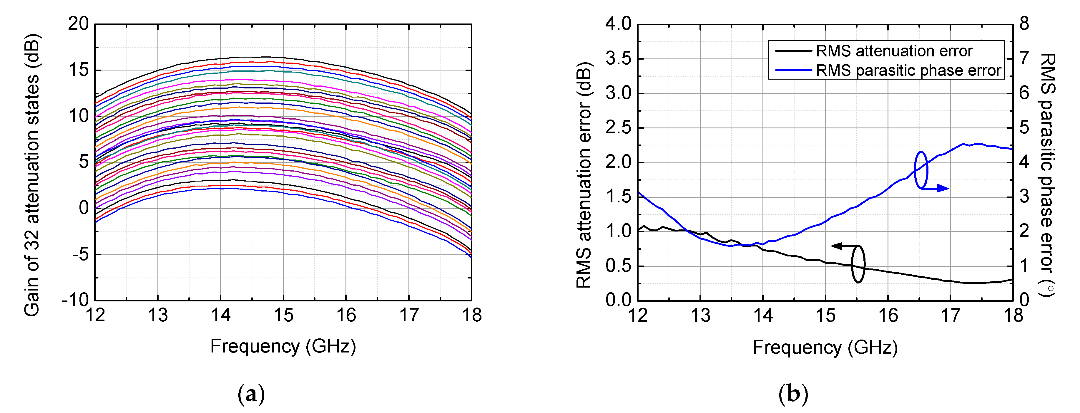
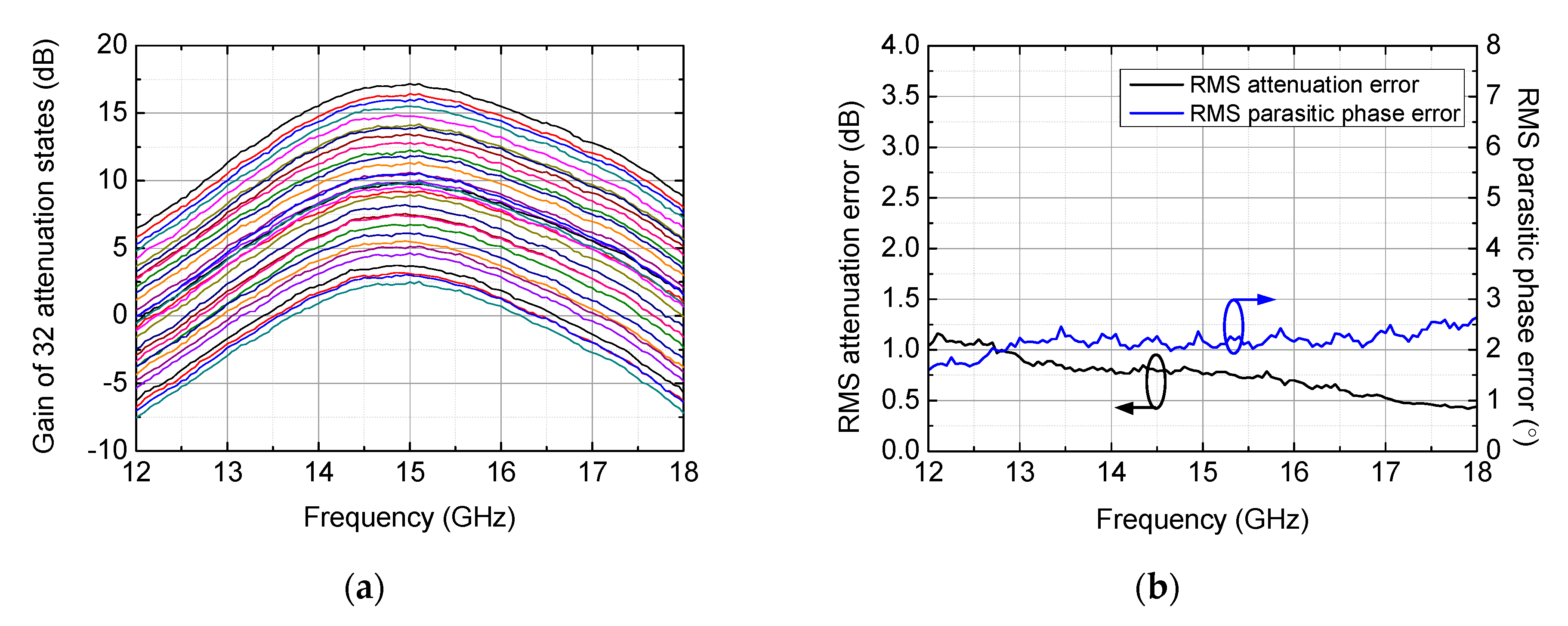
3.1. 5-Bit Digital Attenuator

The attenuator is designed in a passive type for zero DC power consumption. This is beneficial in allowing the multifunction chip to be used in a large-scale phased array system. To achieve a 15.5-dB attenuation range, five-unit attenuator cells with binary-weighted attenuation are connected in cascade. The least significant bit (LSB) and the most significant bit (MSB) are 0.5 dB and 8.0 dB, respectively. In Figure 2, the topologies of the unit attenuator cells are presented. For 0.5-dB and 1.0-dB attenuation, a switched-T structure shown in Figure 2a is adopted for low insertion loss and small chip area. A 2 × 50-μm D-mode HEMT with on-resistance of 12.2 Ω and off-capacitance of 27.3 fF is used for switching devices (Ms and Mp). As the attenuation increases, the conventional switched-T structure presents a larger phase imbalance between the reference and attenuation states. Therefore, a 2.0-dB attenuator cell is designed using the structure shown in Figure 2b. An additional capacitor, CP1, compensates for the phase imbalance by adjusting the insertion phase in the attenuation state without degrading the insertion loss and matching performance in the reference state [15]. Finally, 4.0-dB and 8.0-dB attenuator cells are designed with the structure shown in Figure 2c, where a capacitor, CP2, is connected in parallel with RP2. This not only reduces the phase imbalance but also prevents the bandwidth reduction occurring in high attenuation cells [16,17,18].
Figure 3 shows a full schematic and micrograph of the 5-bit digital attenuator. The placement order of each unit attenuator cell is determined, such that the operation bandwidth is maximized. A shunt resistor (R11) provides the attenuator with DC ground. The 5-bit digital attenuator occupies an area of 0.9 × 0.4 mm2, excluding probing pads. The parameter value of each component is presented in Table 1.
The measurement results of the 5-bit digital attenuator are shown in Figure 4. The insertion loss and matching performance in the reference state are depicted in Figure 4a. The insertion loss ranges from 4.9 to 6.6 dB over the entire Ku-band frequency. The input and output matching are below −14.2 and −23.8 dB, respectively. Figure 4b shows the measured insertion loss for all 32 attenuation states. It can be seen that the total attenuation of 13.8 to 15.5 dB is achieved with a step of 0.5 dB. Figure 4c shows the input and output matching performance for all 32 attenuation states, which are below −11.5 and −15.6 dB, respectively, in the entire Ku-band. The root mean square (RMS) attenuation and parasitic phase errors, shown in Figure 4d, are less than 1 dB and 2°, respectively.

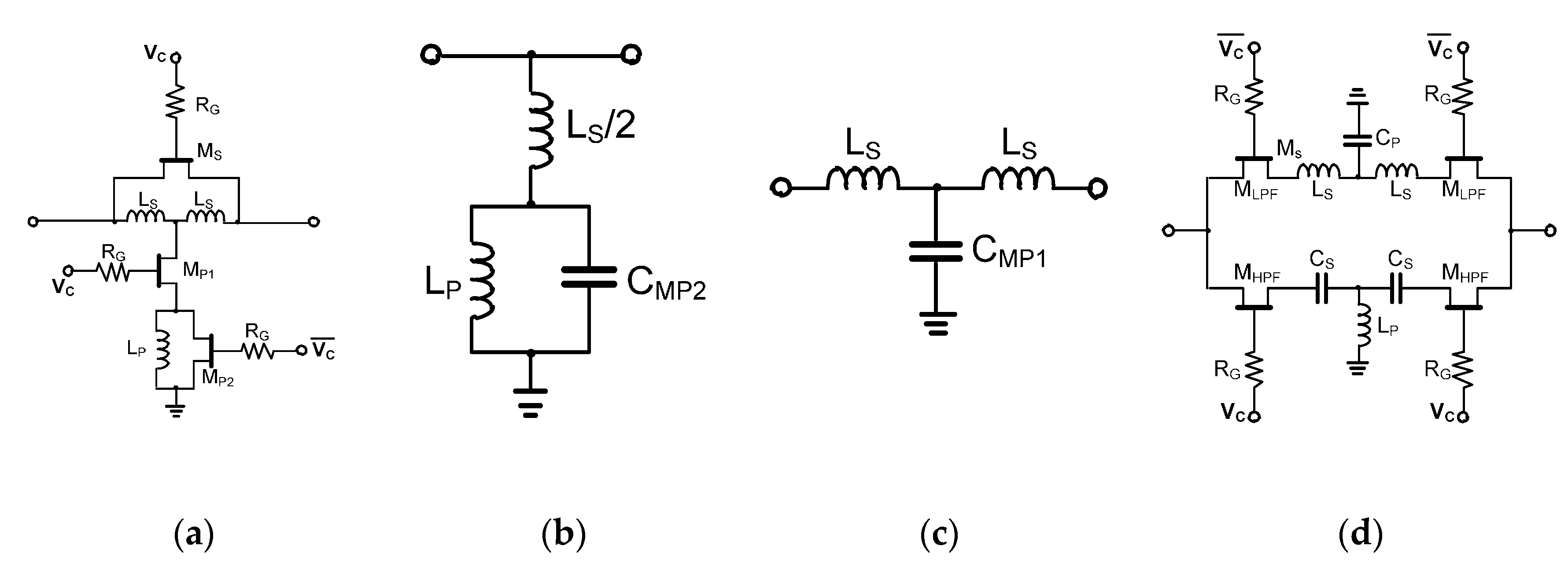
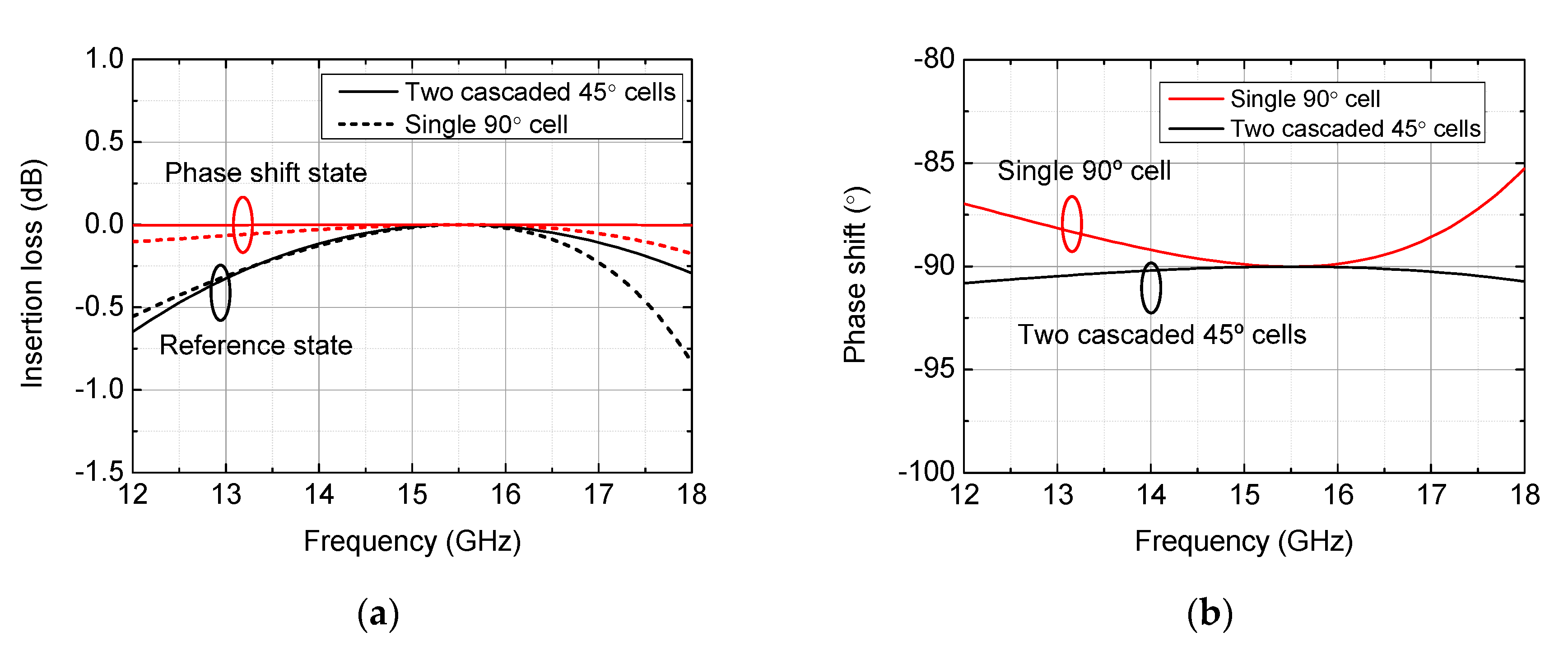
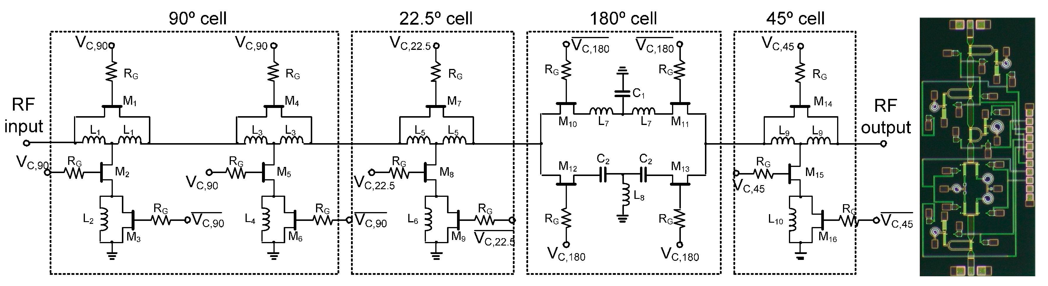
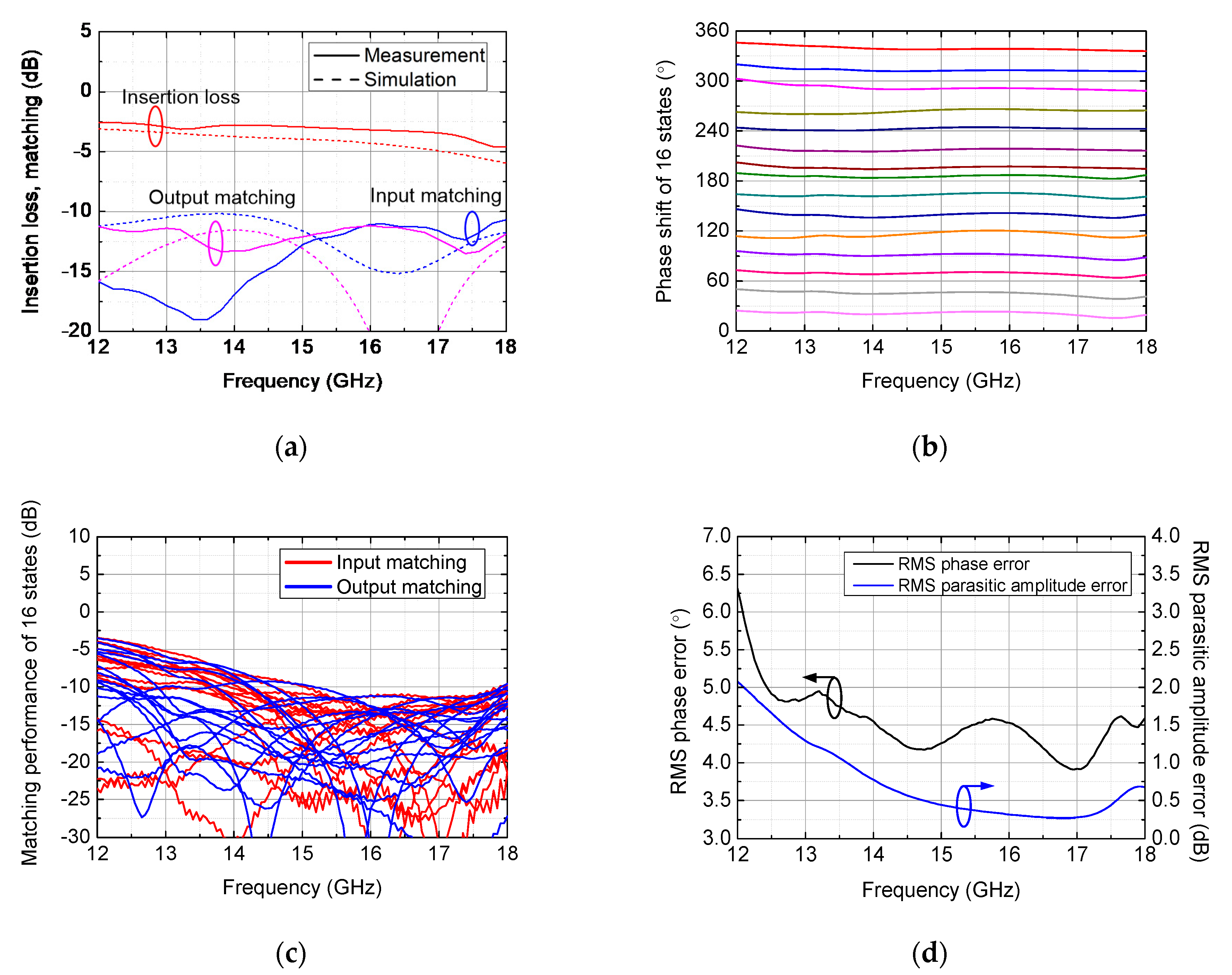
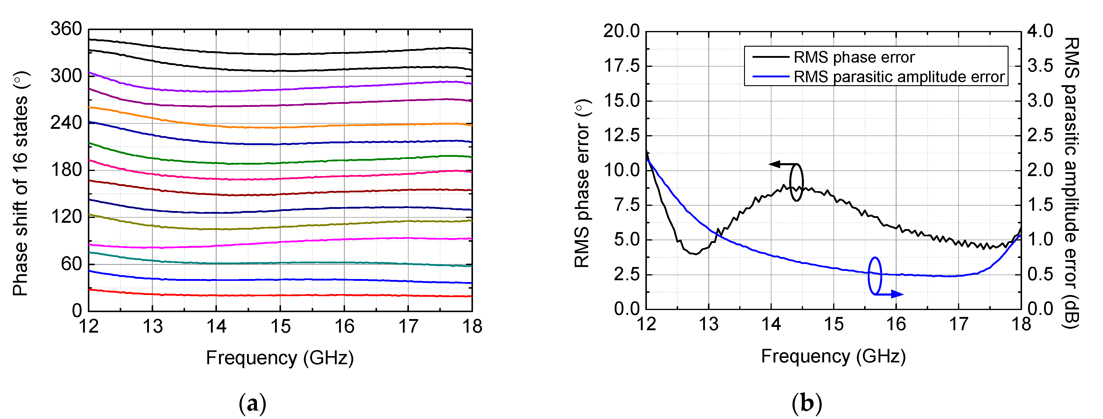
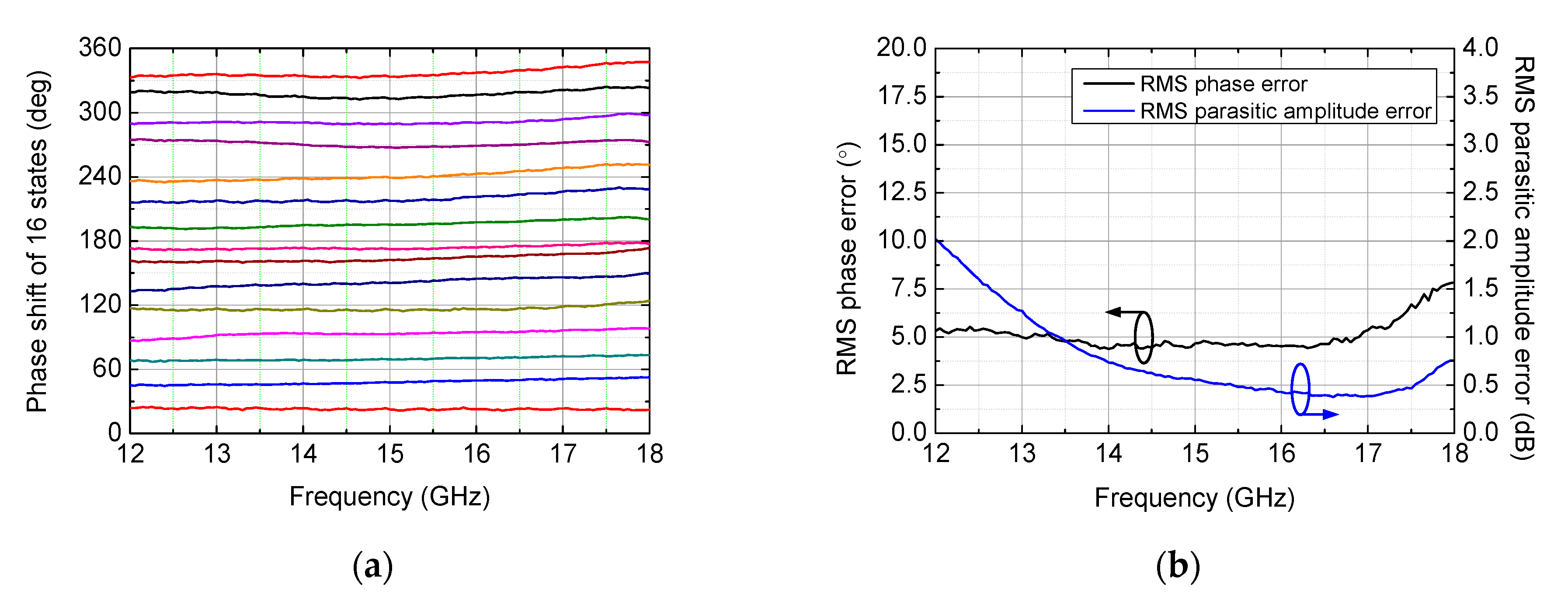
3.2. 4-Bit Digital Phase Shifter

The phase shifter is designed with a passive switched topology to reduce the DC consumption and to facilitate the digital phase control. Four unit cells, each accomplishing phase shifts of 22.5°, 45°, 90° and 180°, are connected in cascade for a full 360° shift.
The 22.5°, 45° and 90° cells adopt a bridged-T structure, as shown in Figure 5a. In the reference state, the transistors, MS and MP1, are turned on while MP2 is turned off, simplifying to the equivalent circuit of Figure 5b. The off-capacitance of MP2 (CMP2) resonates with parallel-connected LP at the operation frequency, giving an open circuit. On the other hand, in the phase-shift state, MS and MP1 are turned off while MP2 is turned on, as shown in Figure 5c. Therefore, the off-capacitance of MP1 (CMP1) and LS provide a designated phase shift. The component values are determined by the following equations [19].
L S = Z 0 ω tan ( ϕ 2 )
L P = 1 ω 2 C MP 2
C MP 1 = sin ( ϕ ) ω Z 0
C MP 2 = 2 L S Z 0 2
where Δϕ is the designated phase shift, Z0 is the characteristic impedance and ω is the operation frequency. It is noted that CMP1 and CMP2 become large as Δϕ increases to 90°. The large off-capacitance requires a large-size transistor, which limits the operation bandwidth. Therefore, the 90° cell is implemented by connecting two 45° cells in cascade. In Figure 6a,b, the insertion loss and phase shift performance are compared, respectively, when a single 90° cell and two cascaded 45° cells are used. Obviously, the two cascaded 45° cells provide a wider bandwidth for 90° phase shift.
A 180° cell is designed using the high-pass filter (HPF)/low-pass filter (LPF) structure shown in Figure 5d. The values of inductance and capacitance are calculated by the following equations [20].
L S = Z 0 tan | ϕ 2 | ω
L P = Z 0 ω sin | ϕ |
C S = 1 ω Z 0 · tan | ϕ 2 |
C P = sin | ϕ | ω Z 0
Figure 7 shows a complete schematic and micrograph of the 4-bit digital phase shifter. The placement order of each unit phase shift cell is optimized for a wide bandwidth and low insertion loss. The 4-bit digital phase shifter test cut occupies an area of 2.6 × 1.1 mm2, excluding probing pads. The parameter value of each component is presented in Table 2.
The measurement results of the 4-bit digital phase shifter are shown in Figure 8. The insertion loss and matching performance in the reference state are depicted in Figure 8a. The insertion loss ranges from 2.5 to 4.5 dB over the entire Ku-band frequency. The input and output matching are below −10.7 and −11.2 dB, respectively. Figure 8b shows the measured phase shift of all 16 states, presenting a full 360° shift in the Ku-band. Figure 8c shows the input and output matching performance for all 16 phase shift states, which are below −5 dB from 13 to 20 GHz. The RMS phase and parasitic amplitude errors, shown in Figure 8d, are less than 6.3° and 2.1 dB, respectively.

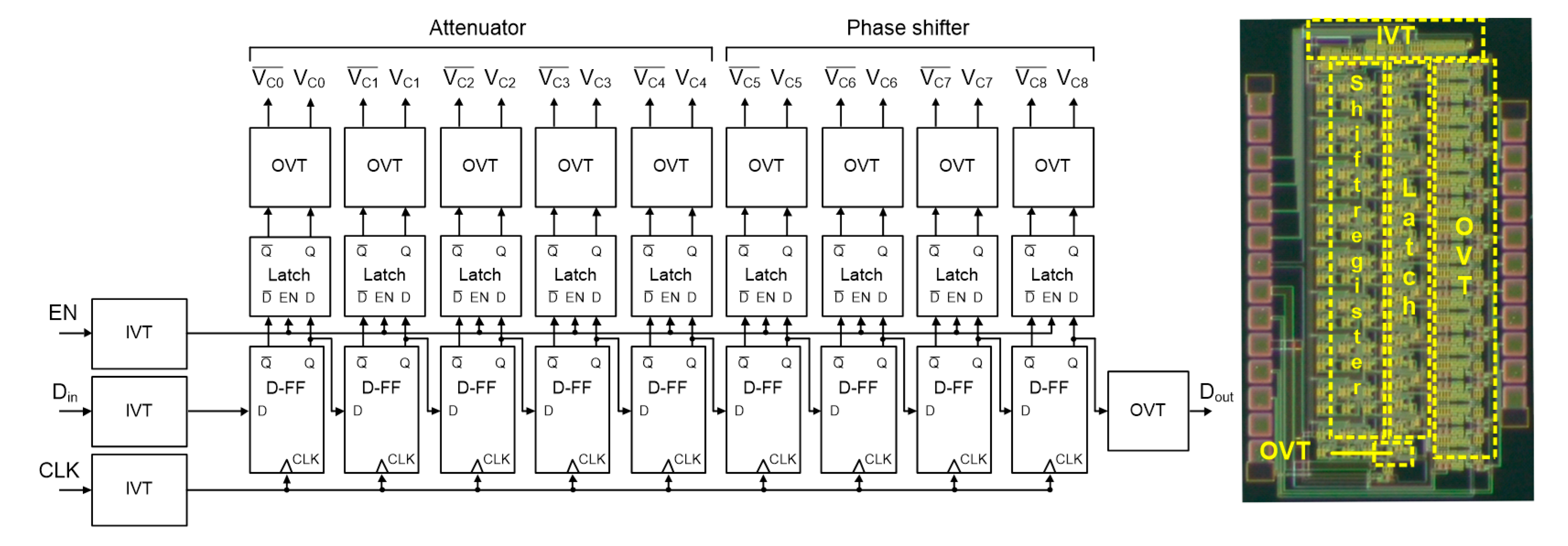
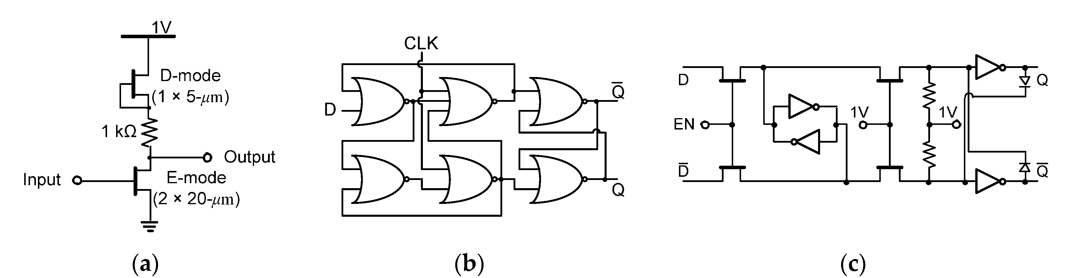
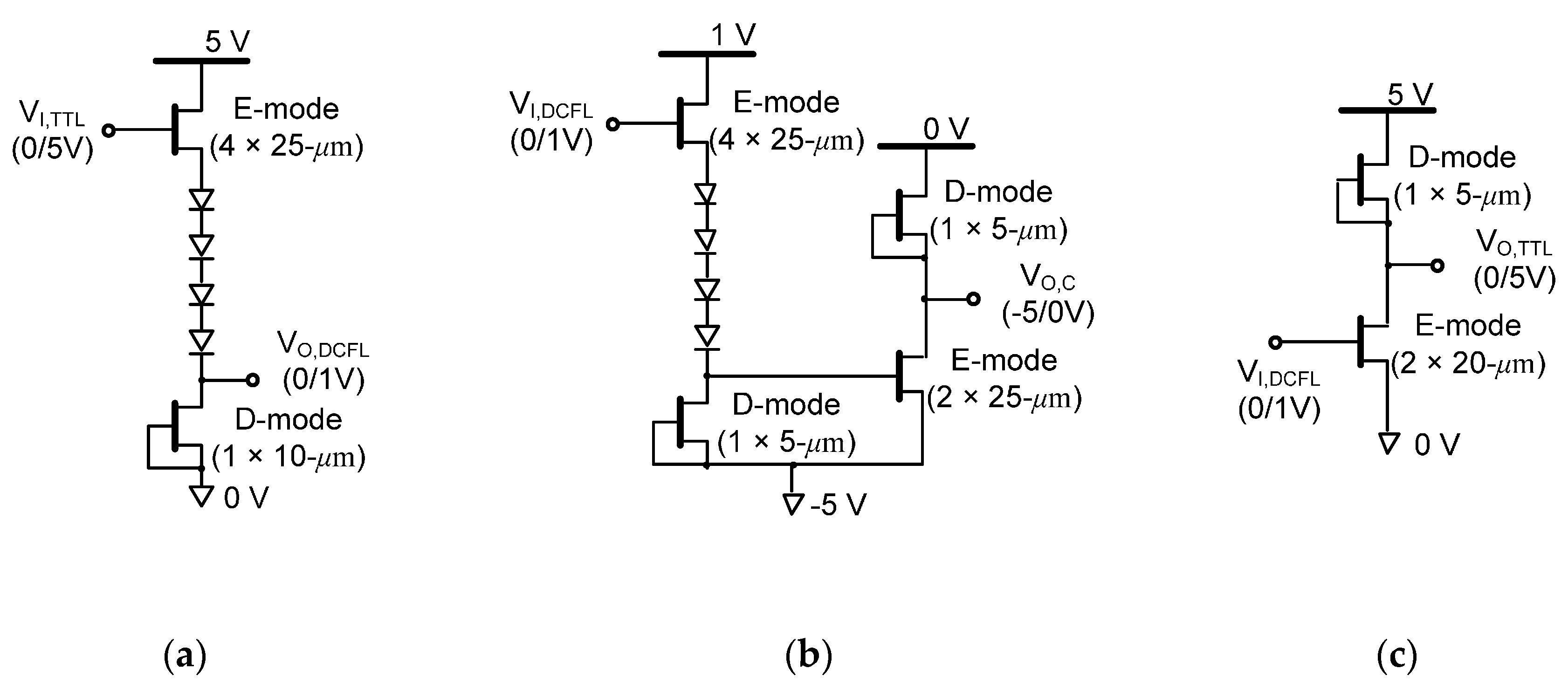
3.3. Serial-to-Parallel Converter (SPC)

As the number of digital control bits increases, the interconnection between the multifunction chip and the digital control unit becomes demanding, especially in a large-scale phased-array system. To alleviate the interconnection complexity, an SPC is integrated into the multifunction chip, which enables serial data input for controlling the 5-bit attenuator and 4-bit phase shifter.
Figure 9 shows a block diagram and micrograph of the 9-bit SPC. It consists of a 9-bit shift register, nine latches, three input voltage transformers (IVT) for serial data input (Din), clock (CLK), enable (EN), nine output voltage transformers (OVT) for control of the attenuator and phase shifter and one OVT for serial data output (Dout).
A simple direct-coupled FET logic (DCFL) is adopted for an inverter due to the small chip area and low DC consumption [21]. As shown in Figure 10a, the inverter consists of an E-mode switching HEMT and a D-mode load HEMT. By adding a 1-kΩ resistor in series with the load transistor, static power consumption can be reduced while sacrificing the switching speed. The static DC current is 0.65 mA. The shift register is based on a conventional D-flip flop, as shown in Figure 10b. Figure 10c shows the schematic diagram of the latch. A diode-coupled feedback is added to the output of the latch. This compensates for the reduced voltage swing caused by the finite on-resistance of the E-mode HEMT of the inverter logic.
The input signals (Din, CLK, EN) follow the Transistor-transistor logic (TTL), which swings from 0 to 5 V. To transform the TTL level to the DCFL inverter level (0 to 1 V), the IVT is designed as shown in Figure 11a. Similarly, two OVTs are designed for two different purposes. The first OVT, shown in Figure 11b, transforms the DCFL level to the control level of the digital attenuator and phase shifter (−5 to 0 V). The second OVT shown in Figure 11c transforms the DCFL level back to the TTL level. The SPC test cut shown in Figure 9 occupies an area of 1.8 × 0.8 mm2, excluding probing pads, and consumes DC power of 350 to 415 mW depending on the input data.

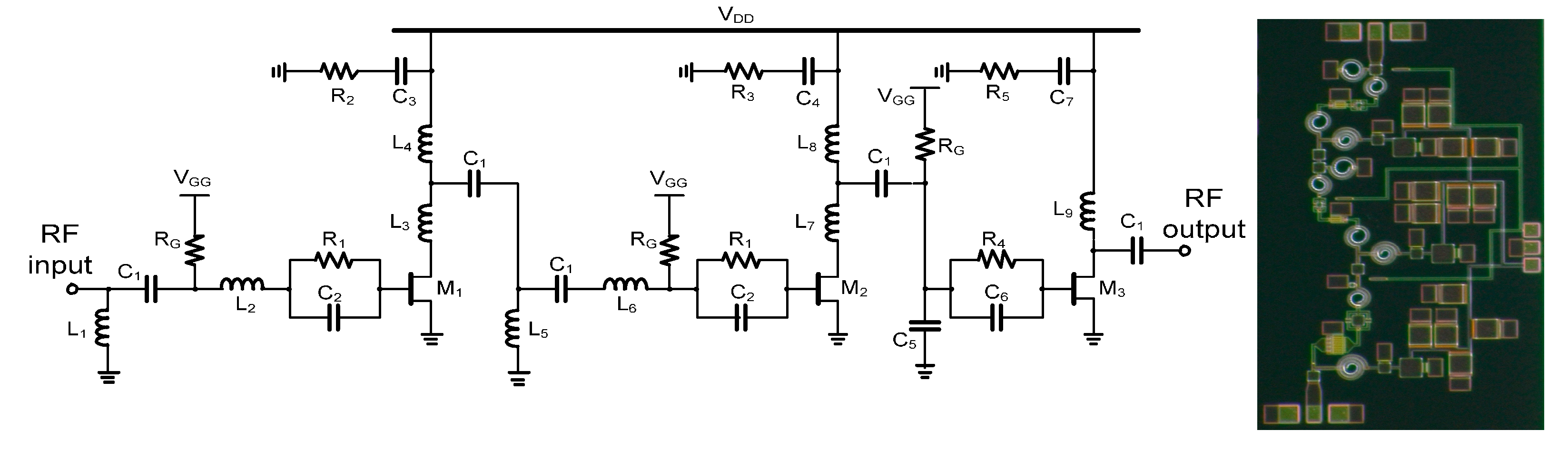
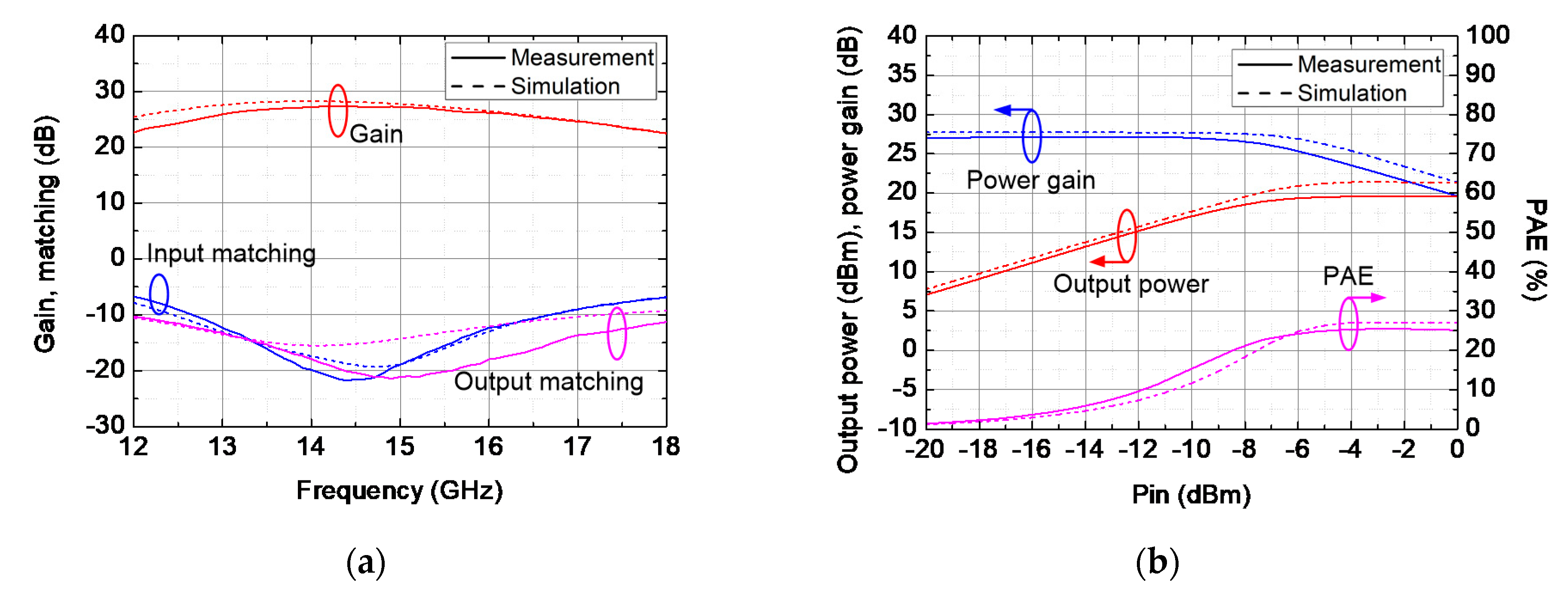
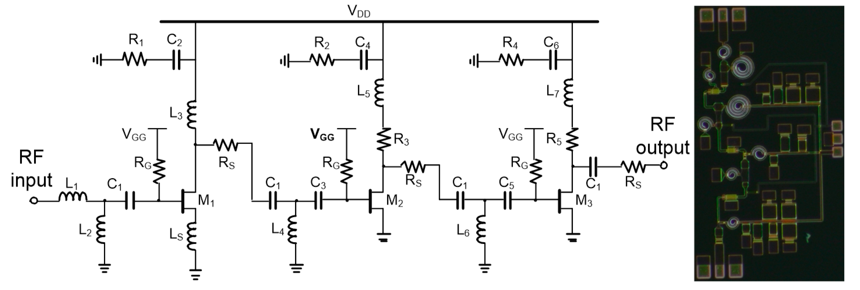
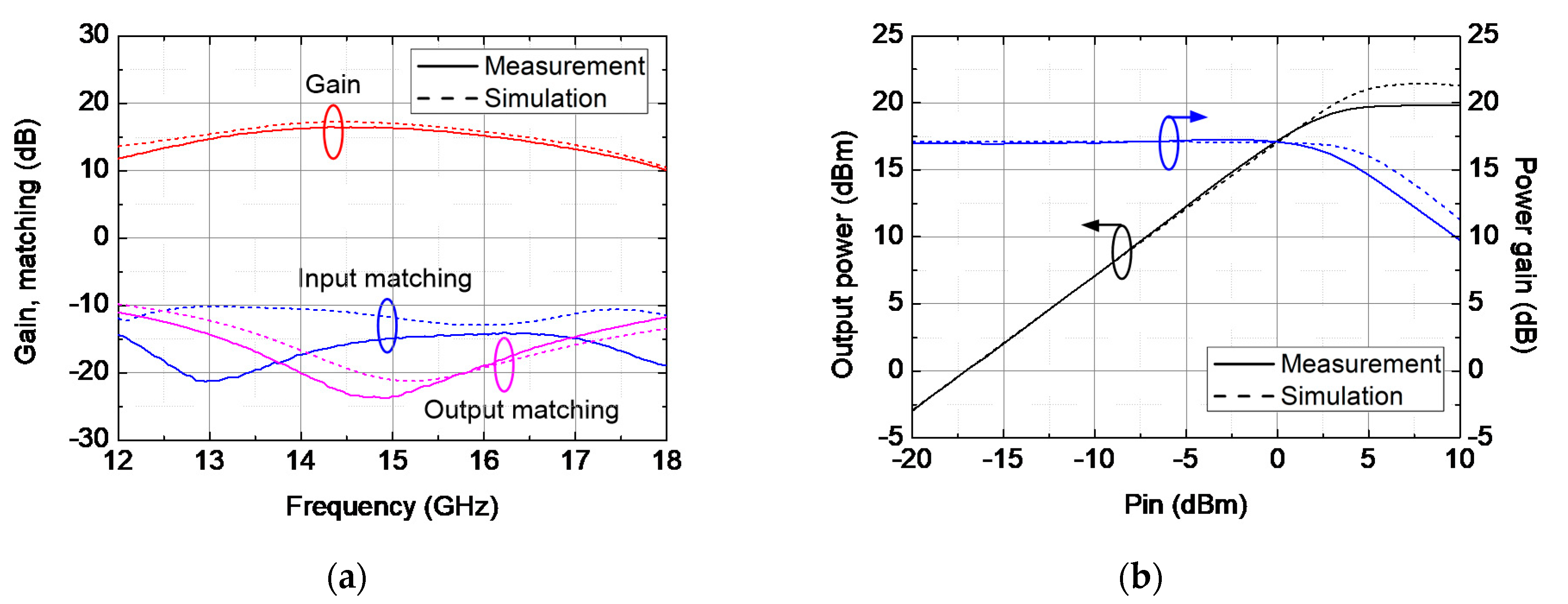
3.4. Medium Power Amplifier (MPA)

A broadband MPA with high gain and output power is designed using E-mode HEMT to compensate for loss from the digital attenuator and digital phase shifter. Figure 12 illustrates a schematic of the MPA.
A three-stage common source topology is adopted to obtain more than 20 dB gain over the Ku-band. In the first two stages, a 2 × 50-μm HEMT (M1, M2) is used for high gain and wide bandwidth. The third stage employs an 8 × 50-μm HEMT (M3) for high output power and linearity. The input is matched to 50 Ω by the L-section network of L1 and L2. Two inter-stage matching networks are implemented using L3-L4-L5-L6 and L7-L8-C5, respectively. The matching frequencies of the networks are intentionally set differently from each other, such that wideband operation is obtained. The output network (L9) is matched to the load-pull impedance for high output power. A parallel R-C network (R1 and C2) is inserted into the signal path to improve the stability at low frequencies. The MPA test cut, as shown in Figure 12, occupies 1.9 × 1.0 mm2, excluding probing pads. The MPA consumes DC power of 380 mW, with a drain bias voltage of 5 V. The measurement results are shown in Figure 13. As shown in Figure 13a, the MPA exhibits a peak gain of 27.3 dB at 14.2 GHz and more than 22.4 dB gain over the Ku-band. The input and output matching are below −6.7 and −10.3 dB, respectively, over the Ku-band. The output power, power gain and power-added efficiency (PAE) at 15 GHz are shown in Figure 13b. The output P1dB (OP1dB) and saturated power (Psat) are 18.9 and 19.6 dBm, respectively. The maximum PAE is 25.5%. A discrepancy between the measurement and simulation is presumably due to inaccuracy of the large-signal transistor model.

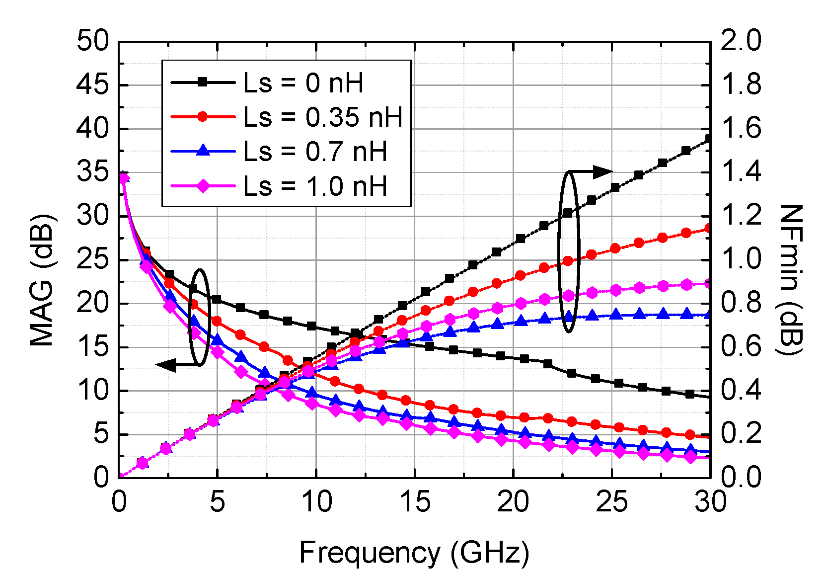
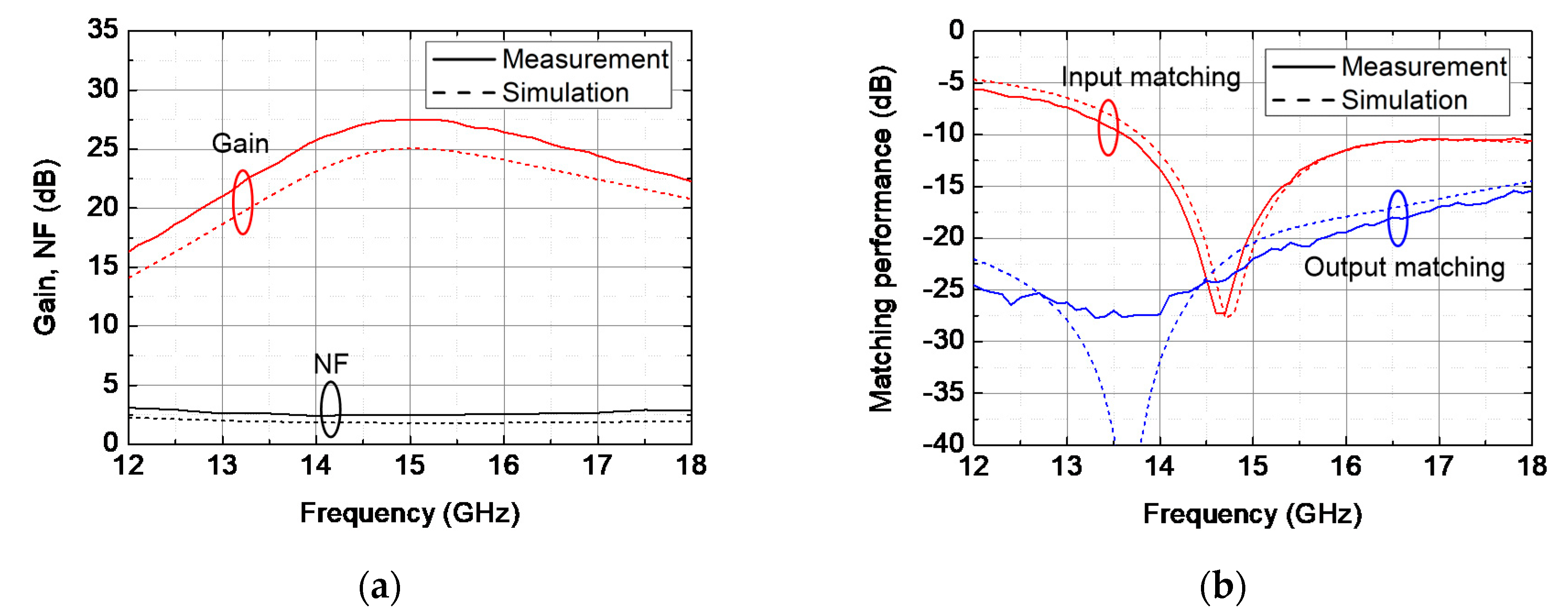
3.5. Low-Noise Amplifier (LNA)

A schematic and micrograph of the Ku-band three-stage LNA is shown in Figure 14. The first two stages employ a 2 × 50-μm HEMT (M1, M2) while the last stage uses a 2 × 75-μm (M3), considering the tradeoff among the gain, noise figure and DC power consumption. The inductive source degeneration (LS) is applied to the first stage for compromising the noise figure, input matching and gain. In Figure 15, the maximum available gain (MAG) and minimum noise figure (NFmin) are simulated with different LS values. With a compromised value of 0.35 nH, the MAG and NFmin exhibit values of 8.6 dB and 0.74 dB, respectively, at 15 GHz. A 10-Ω series resistor (RS) is inserted into the output of each stage to improve the stability.
The LNA test cut occupies an area of 1.6 × 0.9 mm2, excluding probing pads, as shown in Figure 14. The LNA consumes a DC power of 92 mW, with a drain bias voltage of 2 V. Figure 16 shows the measurement results of the LNA. The measured peak gain and noise figure, shown in Figure 16a, are 27.5 dB and 2.4 dB, respectively, at 15 GHz. In Figure 16b, the measured input matching is below −10 dB from 13.7 to 28.5 GHz. The output matching is broadband, below −10 dB, from 3.6 to above 30 GHz, due to the lossy output matching network.

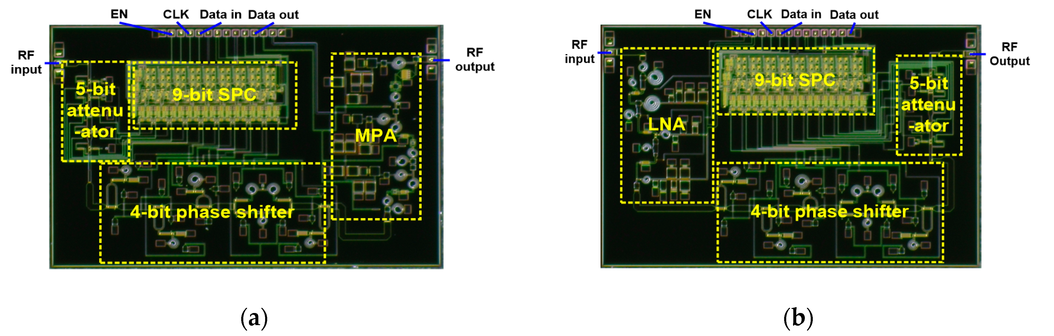
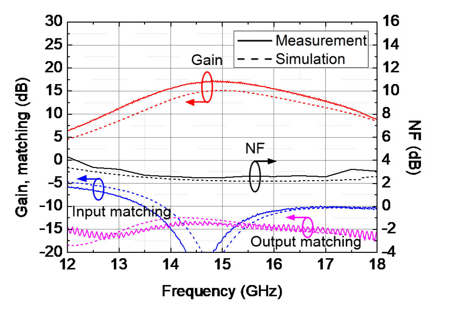
4. Multifunction Transmitter and Receiver

The transmitter and receiver are designed by integrating the circuit blocks described in Section 3. The chip micrographs are shown in Figure 17. Each chip occupies 4.2 × 2.8 mm2, including probing pads. On-wafer probing measurement is performed with a vector network analyzer, noise figure analyzer and power meter. The input digital signals of SPC (Din, CLK, EN) are generated by NI USB-6361 X series multifunction DAQ. To facilitate the measurement for 512 states, the measurement equipment and DAQ are controlled by LABVIEW.
The measured gain, matching and output power of the multifunction transmitter chip are shown in Figure 18. The gain exhibits a peak value of 16.5 dB at 14.7 GHz and more than 10 dB over the Ku-band. The input and output matching are below −10 dB over the Ku-band. The OP1dB and Psat at 15 GHz are 19.2 and 19.8 dBm, respectively.
The measured gains for 32 attenuation states of the multifunction transmitter are depicted in Figure 19a. The gain varies from 1.5 to 16.5 dB at 14.7 GHz. The attenuation range is 13.9 to 15.9 dB over the Ku-band. The RMS attenuation and parasitic phase errors over 32 attenuation states are shown in Figure 19b. The averaged RMS attenuation and parasitic phase error values over the Ku-band are 0.6 dB and 2.9°, respectively.
The measured phase shifts of the multifunction transmitter for 16 phase states are shown in Figure 20a, confirming a full 360° shift. The RMS phase and parasitic amplitude errors over 16 phase states, shown in Figure 20b, are 6.4° and 0.8 dB, respectively, on average, over the Ku-band.
The measured gain, matching and noise figures of the multifunction receiver chip are shown in Figure 21. The multifunction receiver exhibits a peak gain of 17.3 dB and noise figure of 2.5 dB at 15 GHz. The noise figure over the Ku-band is below 4.3 dB. The measured input and output matching are below −7 and −13.2 dB, respectively, over the Ku-band.
The measured gains for the 32 attenuation states of the multifunction receiver are depicted in Figure 22a. The gain varies from 2.5 to 17.3 dB at 15 GHz. The attenuation range is 13.8 to 16 dB over the Ku-band. The RMS attenuation and parasitic phase errors over the 32 attenuation states are shown in Figure 22b. The averaged RMS attenuation and parasitic phase error values over the Ku-band are 0.7 dB and 2.2°, respectively.
The measured phase shifts of the multifunction receiver for the 16 phase states are shown in Figure 23a, confirming a full 360° shift. The RMS phase and parasitic amplitude errors over the 16 phase states, shown in Figure 23b, are 5.1° and 0.8 dB, respectively, on average, over the Ku-band.
In Table 3, the performance of the multifunction transmitter and receiver in this work is summarized and compared with previously reported GaAs multifunction chips. The multifunction transmitter and receiver achieve a high level of integration, including the 5-bit digital attenuator, 4-bit digital phase shifter, 9-bit SPC and amplifier, thus presenting high gain and wideband performance. Moreover, the chipset features relatively high OP1dB and low noise figures over the full Ku-band due to the integration of MPA or LNA.

5. Conclusions

In this paper, a high-gain multifunction transmitter and receiver chipset operating over the Ku-band is presented. MPA and LNA are integrated together with attenuator and phase shifter to achieve high output power and a low noise figure. In addition, SPC is integrated to control the 5-bit attenuator and 4-bit phase shifter, thereby facilitating the digital interconnection. The multifunction chipset was fabricated in a 0.25-μm GaAs pHEMT technology. The measurement results show that the multifunction chipset offers 15.5-dB attenuation with 0.5-dB step and 360° phase shift with 22.5° step. The multifunction transmitter exhibits a peak gain of 16.5 dB and OP1dB of 19.2 dBm. The multifunction receiver exhibits a peak gain of 17.3 dB and noise figure of 2.5 dB. The multifunction chipset can be used for Ku-band phased array systems for military and satellite applications.

Author Contributions

Methodology, H.L., Y.K., K.P., and S.J.; validation, H.L. and S.J.; investigation, H.L., Y.K., I.L., D.K., K.P., and S.J.; resources, H.L., Y.K., I.L., D.K., and K.P.; data curation, H.L., Y.K., I.L., D.K., and K.P.; writing—original draft presentation, H.L., Y.K., D.K., K.P., and S.J.; writing—review and editing, H.L., and S.J.; supervision, S.J.; project administration, S.J.; funding acquisition, S.J. All authors have read and agreed to the published version of the manuscript.

Funding

This research was funded by the MSIT (Ministry of Science and ICT), Korea, under the ITRC (Information Technology Research Center) support program (IITP-2020-0-01749-001) supervised by the IITP (Institute of Information & Communications Technology Planning & Evaluation).

Conflicts of Interest

The authors declare no conflict of interest.

References

  1. Shin, D.H.; Jeong, J.C.; Moon, S.M.; Yom, I.B. Compact Ku-band GaAs Multifunction Chip for SATCOM Phase Arrays. In Proceedings of the 45th European Microwave Conference (EuMC), Paris, France, 7–10 September 2015; pp. 1471–1474. [Google Scholar]
  2. Bugeau, J.; Coughlin, W.; Priolo, M.; Onge, G.S. Advanced MMIC T/R module for 6 to 18 GHz multifunction arrays. In Proceedings of the IEEE 1992 Microwave and Millimeter-Wave Monolithic Circuits Symposium Digest of Papers, Albuquerqu, NM, USA, 1–3 June 1992; pp. 119–122. [Google Scholar]
  3. Jeong, J.C.; Shin, D.H.; Ju, I.; Yom, I.B. An S-Band Multifunction Chip with a Simple Interface for Active Phased Array Base Station Antennas. ETRI J. 2013, 35, 378–385. [Google Scholar] [CrossRef]
  4. Cao, R.; Li, Z.; Tao, X.; Sang, L. A compact X-band four-channel SiGe BiCMOS T/R chipset for digital array radar applications. In Proceedings of the IEEE MTT-S International Microwave Symposium (IMS), Honololu, HI, USA, 4–9 June 2017; pp. 1979–1982. [Google Scholar]
  5. Carosi, D.; Bentini, A.; Nanni, A.; Marescialli, L.; Cetronio, A. Mixed-signal X-band SiGe multi-function control MMIC for phased array radar applications. In Proceedings of the European Microwave Conference (EuMC), Rome, Italy, 29 September–1 October 2009; pp. 240–243. [Google Scholar]
  6. Jeong, J.C.; Yom, I.B. X-band High power SiGe BiCMOS multi-function chip for active phased array radars. Electron. Lett. 2011, 47, 618–619. [Google Scholar] [CrossRef]
  7. Cho, M.K.; Han, J.H.; Kim, J.H.; Kim, J.G. An X/Ku-band bi-directional true time delay T/R chipset in 0.13 μm CMOS technology. In Proceedings of the IEEE MTT-S International Microwave Symposium (IMS), Tampa, FL, USA, 1–6 June 2014; pp. 1–3. [Google Scholar]
  8. Kim, D.S.; Yeon, K.W. Compact 4-bit GaAs Ku-band core chips for phased arrays. Microw. Opt. Technol. Lett. 2020, 62, 2289–2299. [Google Scholar] [CrossRef]
  9. Zhou, S.; Zhou, S.; Zhang, J.; Wu, J.; Yang, H.; Wang, Z. A 7.5–9 GHz GaAs two-channel multi-function chip. Electronics 2019, 8, 395. [Google Scholar] [CrossRef] [Green Version]
  10. Ciccognani, W.; Ferrari, M.; Ghione, G.; Limiti, E.; Longhi, P.E.; Pirola, M.; Quaglia, R. A compact high performance X-Band core-chip with on board serial-to-parallel conversion. In Proceedings of the 40th European Microwave Conference (EuMC), Paris, France, 28–30 September 2010; pp. 902–905. [Google Scholar]
  11. Bentini, A.; Ferrari, M.; Longhi, P.E.; Marzolf, E.; Moron, J.; Leblanc, R. A 6–18 GHz GaAs multifunctional chip for transmit/receive modules. In Proceedings of the 44th European Microwave Conference (EuMC), Rome, Italy, 8–10 October 2014; pp. 1908–1911. [Google Scholar]
  12. Jeong, J.C.; Uhm, M.; Jang, D.P.; Yom, I.B. A Ka-band GaAs multi-function chip with wide-band 6-bit phase shifters and attenuators for satellite applications. In Proceedings of the 13th European Conference of Antennas and Propagation (EuCAP), Krakow, Poland, 31 March–5 April 2019; pp. 1–4. [Google Scholar]
  13. Van Vliet, F.E.; Van Wanum, M.; Roodnat, A.W. Fully-integrated wideband TTD core chip with serial control. In Proceedings of the Gallium Arsenide applications symposium (GAAS), Munich, German, 6–10 October 2003; pp. 89–92. [Google Scholar]
  14. Pirola, M.; Quaglia, R.; Ghione, G.; Ciccognani, W.; Limiti, E. 13-bit GaAs serial-to-parallel converter with compact layout for core-chip applications. Microelecron. J. 2014, 45, 864–869. [Google Scholar] [CrossRef]
  15. Zhang, L.; Zhao, C.; Zhang, X.; Wu, Y.; Kang, K. A CMOS K-band 6-bit attenuator with low phase imbalance for phased array applications. IEEE Access 2017, 5, 19657–19661. [Google Scholar] [CrossRef]
  16. Sun, P. Analysis of phase variation of CMOS digital attenuator. Electron. Lett. 2014, 50, 1912–1914. [Google Scholar] [CrossRef]
  17. Song, I.; Cho, M.; Cressler, J.D. Design and analysis of a low loss, wideband digital step attenuator with minimized amplitude and phase variations. IEEE J. Solid State Circuits 2018, 53, 2202–2213. [Google Scholar] [CrossRef]
  18. Luo, L.; Li, Z.; Yao, Y.; Cheng, G. A 6-Bit Ku Band Digital Step Attenuator with Low Phase Variation in 0.13-μm SiGe BiCMOS. Electronics 2019, 8, 1149. [Google Scholar] [CrossRef] [Green Version]
  19. Kang, D.W.; Lee, H.D.; Kim, C.H.; Hong, S. Ku-band MMIC phase shifter using a parallel resonator with 0.18-μm CMOS technology. IEEE Trans. Microw. Theory Tech. 2006, 54, 294–301. [Google Scholar] [CrossRef]
  20. Bahl, I.J.; Bhartia, P. Microwave Solid State Circuit Design; John Wiley & Sons: New York, NY, USA, 1988. [Google Scholar]
  21. Yanyang, X.; Xiaoguang, Z.; Jingchen, H. Direct coupled FET logic (DCFL) circuit for GaAs LSIC application. In Proceedings of the 1998 International Conference of Microwave and Millimeter Wave Technology (ICMMT’98), Beijing, China, 18–20 August 1998; pp. 913–916. [Google Scholar]
Figure 1. Block diagram of (a) the Ku-band multifunction transmitter and (b) receiver.
Electronics 09 01327 g001
Figure 2. Topologies of the unit attenuator cells. (a) 0.5-dB and 1-dB attenuator cell, (b) 2-dB attenuator cell, (c) 4-dB and 8-dB attenuator cell.
Electronics 09 01327 g002
Figure 3. Schematic and chip micrograph of the 5-bit digital attenuator.
Electronics 09 01327 g003
Figure 4. Measurement results of the 5-bit digital attenuator: (a) insertion loss and matching performance in the reference state, (b) insertion loss for all 32 attenuation states, (c) input and output matching for all 32 attenuation states, (d) root mean square (RMS) attenuation and parasitic phase errors.
Electronics 09 01327 g004
Figure 5. (a) Bridged-T structure for 22.5°, 45° and 90° unit cells, (b) equivalent circuit in the reference state, (c) equivalent circuit in the phase shift state, (d) high-pass-filter/low-pass-filter structure for 180° unit cell.
Electronics 09 01327 g005
Figure 6. Performance comparison of two structures implementing 90° phase shift: (a) insertion loss, (b) phase shift.
Electronics 09 01327 g006
Figure 7. Schematic and chip micrograph of the 4-bit digital phase shifter.
Electronics 09 01327 g007
Figure 8. Measurement results of the 4-bit digital phase shifter: (a) insertion loss and matching performance in the reference state, (b) phase shift for all 16 states, (c) input and output matching for all 16 states, (d) RMS phase and parasitic amplitude errors.
Electronics 09 01327 g008
Figure 9. Block diagram and chip micrograph of the 9-bit SPC.
Electronics 09 01327 g009
Figure 10. Schematics of (a) the inverter, (b) shift register, (c) latch.
Electronics 09 01327 g010
Figure 11. Schematics of (a) input voltage transformers (IVT), (b) output voltage transformers (OVT) for controlling the digital attenuator and phase shifter, (c) OVT for Dout.
Electronics 09 01327 g011
Figure 12. Schematic and chip micrograph of the medium power amplifier (MPA).
Electronics 09 01327 g012
Figure 13. Measurement results of the MPA. (a) Gain and matching performance, (b) output power, power gain and power-added efficiency (PAE) versus input power at 15 GHz.
Electronics 09 01327 g013
Figure 14. Schematic and chip micrograph of the low-noise amplifier (LNA).
Electronics 09 01327 g014
Figure 15. Simulated maximum available gain (MAG) and minimum noise figure (NFmin) of the 2 × 50-μm transistor with various values of LS.
Electronics 09 01327 g015
Figure 16. Measurement results of the LNA. (a) Gain and noise figure, (b) input and output matching.
Electronics 09 01327 g016
Figure 17. Chip micrographs of (a) the multifunction transmitter, (b) receiver.
Electronics 09 01327 g017
Figure 18. Measurement results of the multifunction transmitter in the reference state: (a) gain and matching performance, (b) output power and power gain versus input power at 15 GHz.
Electronics 09 01327 g018
Figure 19. Attenuation performance of the multifunction transmitter: (a) gain in the 32 attenuation states, (b) RMS attenuation and parasitic phase errors.
Electronics 09 01327 g019
Figure 20. Phase shift performance of the multifunction transmitter: (a) phase shift in the 16 phase states, (b) RMS phase and parasitic amplitude errors.
Electronics 09 01327 g020
Figure 21. Measured gain, noise figure and matching performance of the multifunction receiver.
Electronics 09 01327 g021
Figure 22. Attenuation performance of the multifunction receiver: (a) gain in the 32 attenuation states, (b) RMS attenuation and parasitic phase errors.
Electronics 09 01327 g022
Figure 23. Phase shift performance of the multifunction receiver: (a) phase shift in the 16 phase states, (b) RMS phase and parasitic amplitude errors.
Electronics 09 01327 g023
Table 1. Design parameters of the 5-bit digital attenuator.
ParameterDesign ValueParameterDesign ValueParameterDesign Value
M1–M102 × 50-μmR55.1 ΩR10498.9 Ω
R116.4 ΩR6627.0 ΩR11, RG6.7 kΩ
R2102.3 ΩR77.6 ΩC165.3 fF
R331.5 ΩR8371.2 ΩC2133.9 fF
R496.9 ΩR918.4 ΩC3122.8 fF
Table 2. Design parameters of the 4-bit digital phase shifter.
ParameterDesign ValueParameterDesign Value
M1, M4, M8, M9, M145 × 75-μmL1, L3, L9212.7 pH
M2, M5, M7, M10, M11, M12, M13, M155 × 125-μmL2, L4, L10619.7 pH
M3, M6, M169 × 100-μmL5102.1 pH
RG2.1 kΩL61.3 nH
C1, C2205.4 fFL7, L8513.4 pH
Table 3. Performance summary and comparison.
Ref.ProcessFreq. (GHz)ArchitectureGainMAX 1 (dB)OP1dB (dBm)NF 2(dB)PS/ATT 3(# of bits)RMS Atten. Error 4 (dB)RMS Phase Error 5 (°) Chip Size
(mm2)
[1]0.5-μm GaAs pHEMT12–18ATT + PS + SPC−13--4/40.53.57.6
[8]0.25-μm GaAs pHEMT10.5–13LNA + PS + SPC12 *3.3@12.25GHz24/--<63.0
[8]0.25-μm GaAs pHEMT13.5–15.5PS + DA 6 + SPC>1012.5@14.5GHz-4/--<33.0
[10]0.18-μm GaAs pHEMT8.6–10SW + AMPTx 7 + AMPRx 8 + ATT + PS + SPC11.9 (Tx)
12.3 (Rx)
--6/6--14.8
[11]0.18-μm GaAs pHEMT6–18SW + AMPTx + AMPRx + ATT + PS + SPC23.5 *>1784/40.5825.8
This work0.25-μm GaAs pHEMT12–18ATT + PS + MPA + SPC16.519.2@15GHz 4/50.66.411.7
This work0.25-μm GaAs pHEMT12–18LNA + ATT + PS + SPC17.3 4.34/50.75.111.7
1 Maximum gain over the bandwidth. 2 Maximum noise figure over the bandwidth. 3 Phase shifter/attenuator. 4 Averaged RMS attenuation error. 5 Averaged RMS phase error. 6 Drive amplifier. 7 Transmitter amplifier. 8 Receiver amplifier. * The value is estimated from plots in the article.

