Article

On-Chip Terahertz Detector Designed with Inset-Feed Rectangular Patch Antenna and Catadioptric Lens

1
Department of Microelectronics and Solid-state Electronics, School of Electrical and Information Engineering, Tianjin University, Tianjin 300072, China
2
Department of Microelectronics and Solid-state Electronics, School of Microelectronics, Tianjin University, Tianjin 300072, China
3
Department of Electrical Engineering, Faculty of Engineering, University of Malaya, Kuala Lumpur 50603, Malaysia
*
Author to whom correspondence should be addressed.
Electronics 2020, 9(6), 1049; https://doi.org/10.3390/electronics9061049
Submission received: 6 May 2020 / Revised: 18 June 2020 / Accepted: 19 June 2020 / Published: 24 June 2020
(This article belongs to the Special Issue Terahertz Technology and Its Applications)

Abstract

:
This study proposes an on-chip terahertz (THz) detector designed with on-chip inset-feed rectangular patch antenna and catadioptric lens. The detector incorporates a dual antenna and dual NMOSFET structure. Radiation efficiency of the antenna reached 89.4% with 6.89 dB gain by optimizing the antenna inset-feed and micro-strip line sizes. Simulated impedance was 85.55 − j19.81 Ω, and the impedance of the antenna with the ZEONEX horn-like catadioptric lens was 117.03 − j20.28 Ω. Maximum analyzed gain of two on-chip antennas with catadioptric lens was 17.14 dB resonating at 267 GHz. Maximum experimental gain of two on-chip patch antennas was 4.5 dB at 260 GHz, increasing to 10.67 dB at 250 GHz with the catadioptric lens. The proposed on-chip rectangular inset-feed patch antenna has a simple structure, compatible with CMOS processing and easily implemented. The horn-like catadioptric lens was integrated into the front end of the detector chip and hence is easily molded and manufactured, and it effectively reduced terahertz power absorption by the chip substrate. This greatly improved the detector responsivity and provided very high gain. Corresponding detector voltage responsivity with and without the lens was 95.67 kV/W with NEP = 12.8 pW/Hz0.5 at 250 GHz, and 19.2 kV/W with NEP = 67.2 pW/Hz0.5 at 260 GHz, respectively.

1. Introduction

Terahertz (THz) detectors have been recently employed to assist security aspects for high-speed data communication, spectroscopy, concealed weapon detection, short-range radar, aviation assistance, cancer detection, and many more applications [1,2,3,4]. The THz spectrum region is in the middle of the microwave and infrared spectra and is sometimes known as sub-millimeter waves. Terahertz radiation ranges from 3 mm to 30 µm with corresponding frequencies of 0.1–10 THz [5,6,7,8,9], which penetrate plastics, paper, and wood. The THz region is sometimes called the “THz Gap” [10,11,12] because optical and microwave theory do not fully apply for this frequency range.
Specific terahertz antennas are required to radiate and receive terahertz waves, acting as transducers to convert high-frequency current or waveguide energy into spatial electromagnetic wave energy, and directional radiation for transmission or the reverse conversion for receiving. However, designing an on-chip antenna in the terahertz band is somewhat difficult, partly because the system’s dynamic range and transmission distance between the THz wave source and detector are influenced by antenna gain. Dielectric layers between the CMOS top and bottom metal layers are too thin to construct a high gain antenna [13,14], and lossy silicon substrates significantly reduce on-chip patch antenna performance. However, problems can be solved with reasonable on-chip antenna design considering antenna gain and bandwidth.
Annular on-chip single-ended slot antennas can achieve approximately 4.5 dB gain with 50% radiation efficiency [15]. Although directional front-end antennas are unsuitable for THz detectors [16,17], Taeguk log periodic dipole antennas (LPDAs) can achieve a maximum 7.8 dBi gain at 73 GHz and circular LPDA antennas can achieve a maximum 9.25 dBi gain at 85 GHz [17,18]. The total size of these two antennas is 4.5 × 10 mm2 and they have complicated structures. Rectangular antennas are the most common on-chip design, leveraging simple structure and being compatible with standard CMOS processing [18,19]. The proposed rectangular antenna from [20] was 237.5 × 317 μm2 and operated at 300 GHz, but only achieved −2.1 dB gain. In contrast, the proposed THz dielectric resonator antenna (DRA) [21] employed a 500 µm resonator to greatly enhance antenna gain. The DRA was 290–310 µm wide and 390–410 µm long, considerably larger than the traditional rectangular patch antenna, and provided measured 6.7 dB maximum gain at 327 GHz. Thus, there is considerable ongoing research to improve THz detector antenna gain.
This study proposes an on-chip terahertz detector with on-chip rectangular inset-feed patch antennas that was implemented using a United Microelectronics Corporation (UMC) 0.18 μm standard CMOS process and ZEONEX RS420 (ZEON Corporation, Tokyo, Japan) horn-like catadioptric lens. Section 2 discusses the antenna design and Section 3 introduces the detector structure, combining plasma wave-based terahertz detection in NMOSFETs (TeraFETs). Section 4 describes the horn-like catadioptric lens and Section 5 details testing for the prototype proposed THz detector antenna and lens. Conclusions are presented in Section 6.

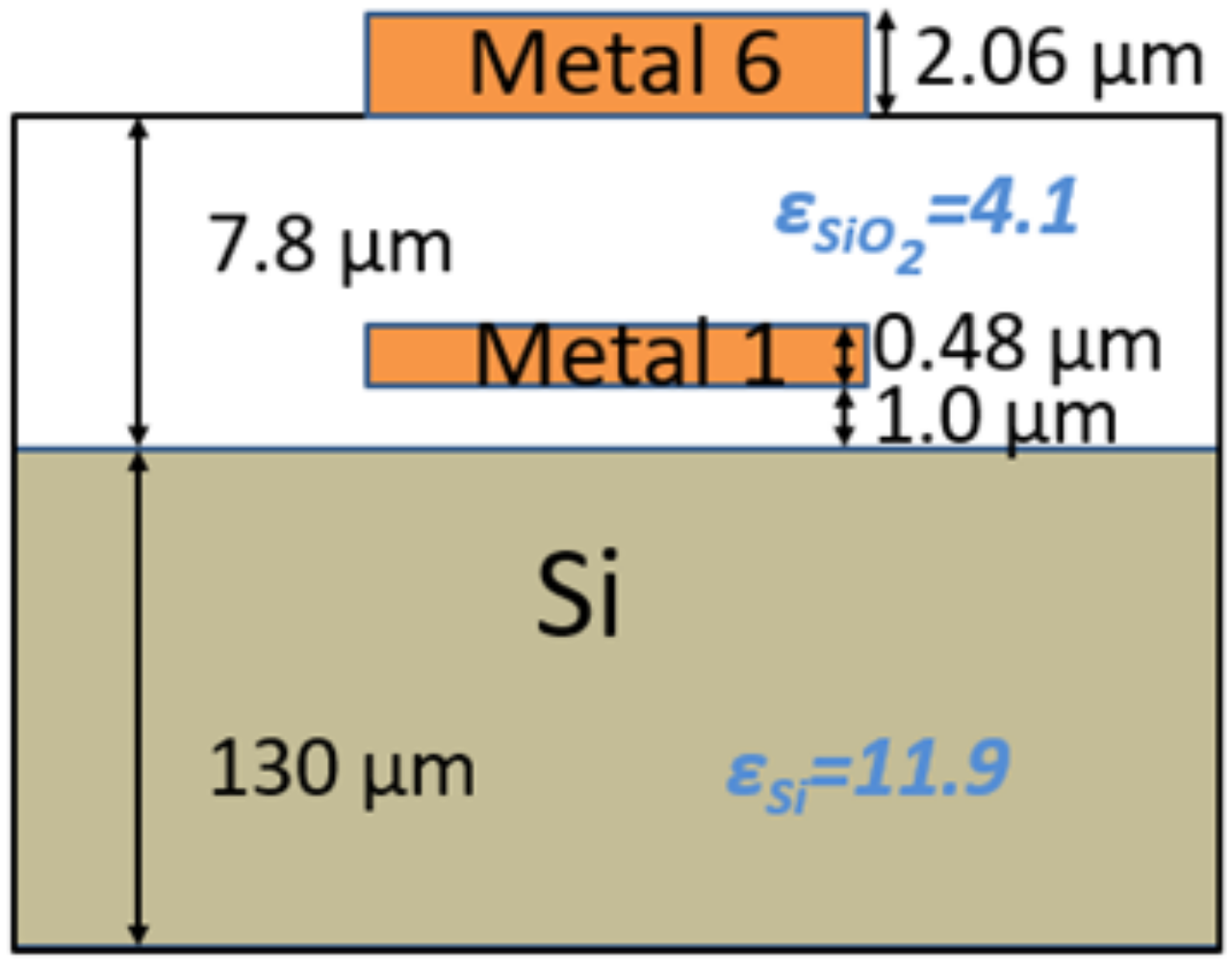
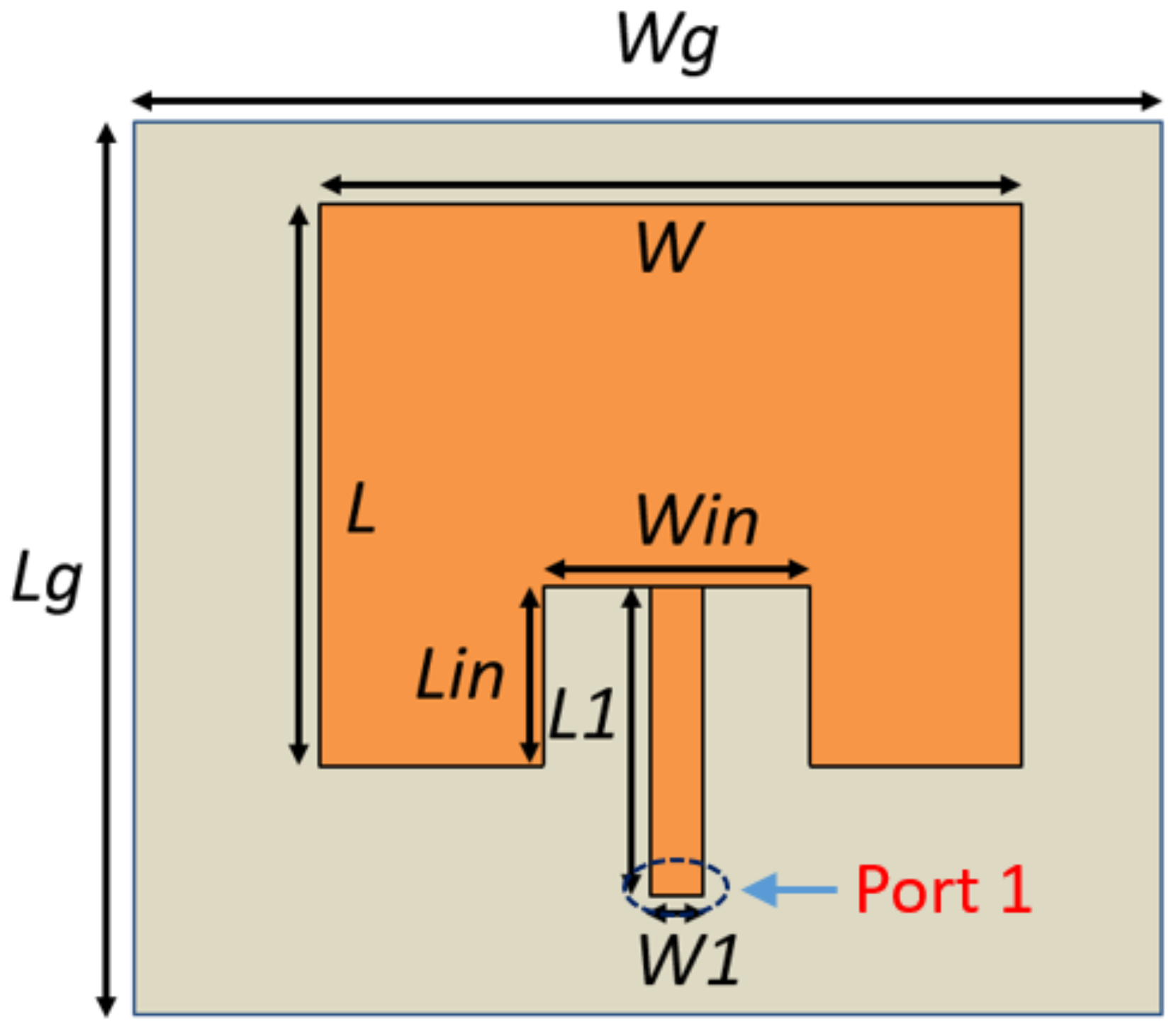
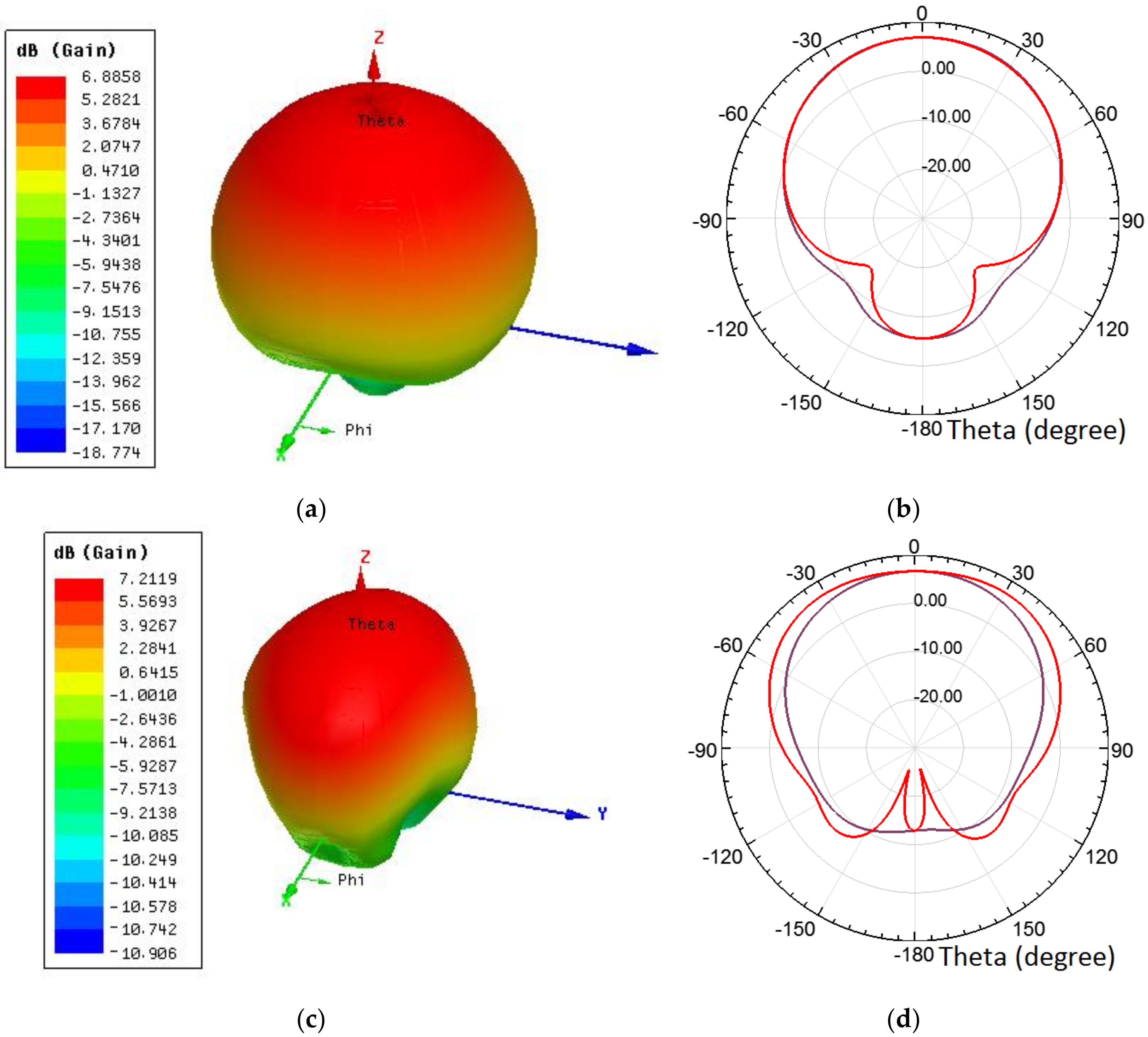
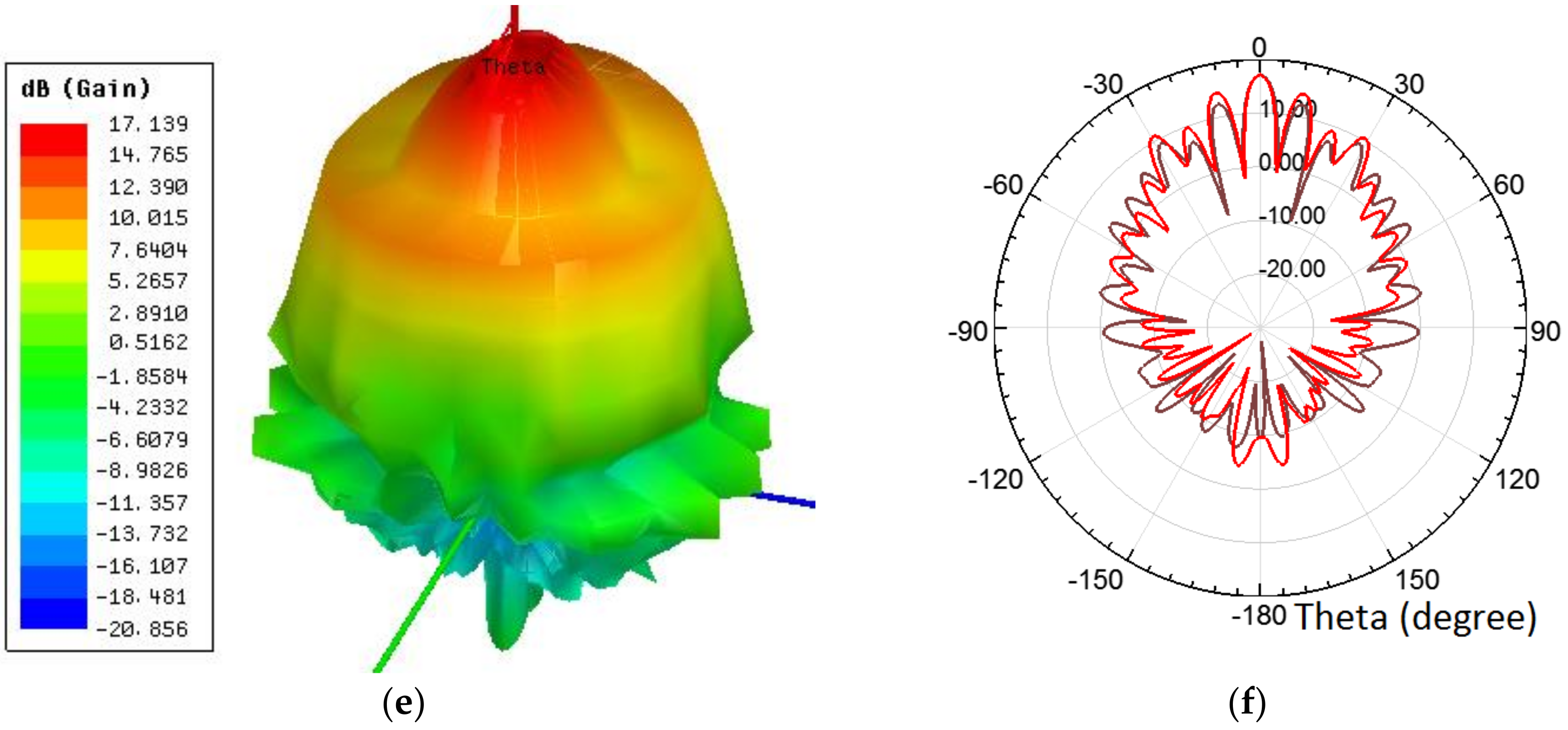
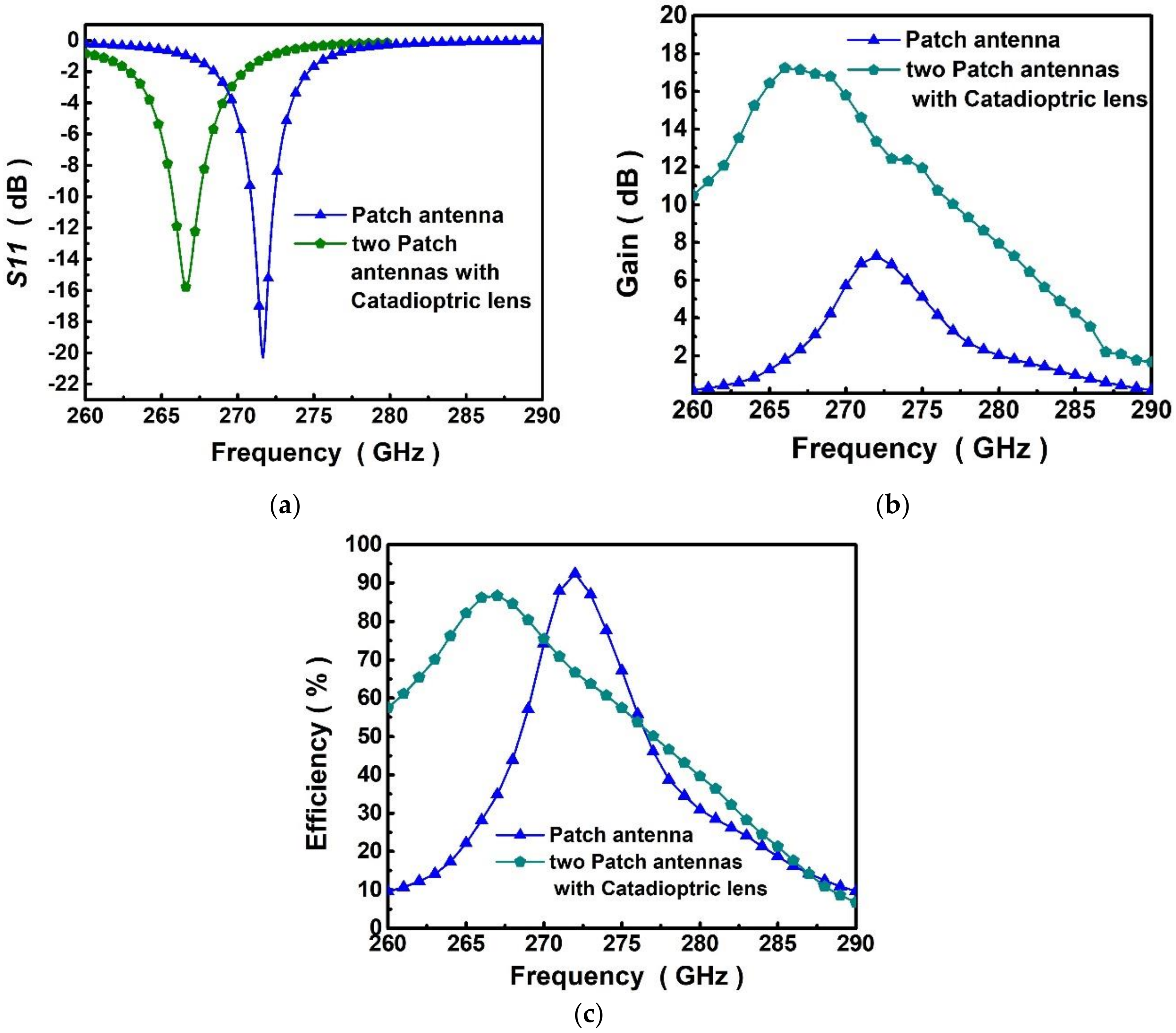
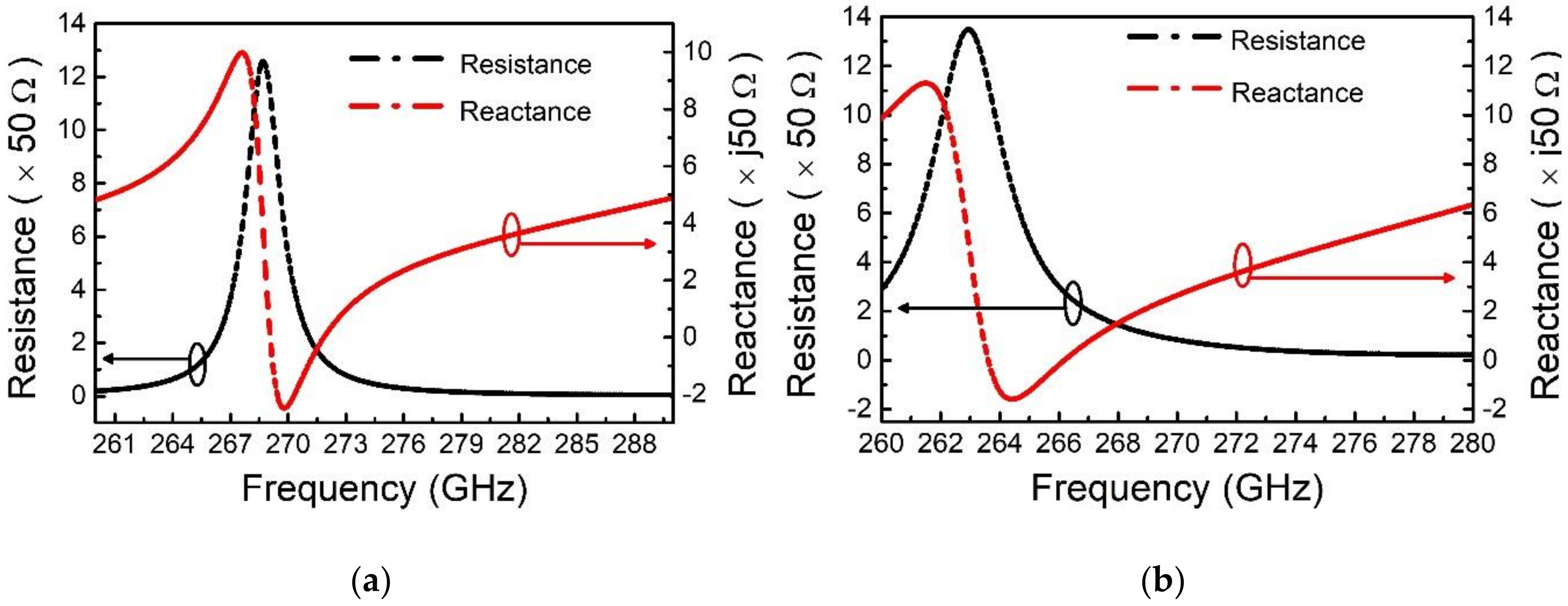
2. On-Chip THz Antenna

The UMC 0.18 μm CMOS process provides six metal layers with intermediate dielectric layers (SiO2) between them. The CMOS process can be used to design not only digital and analog circuits, but also optoelectronic devices [22,23,24]. The major advantage is that signals detected by the detector can be amplified and processed on the chip. However, silicon is lossy in the THz frequency range due to the short wavelength. Therefore, we implemented the antenna inset-feed patch in the Metal 6 (top metal) layer, using the Metal 1 (bottom metal) layer as a ground plane to reflect radiated power back to the NMOSFETs, hence reducing THz signal penetration into the lossy silicon substrate [20,21]. Metal 6 is 2.06 µm thick and the SiO2 CMOS process layer is 6.32 µm thick. Radiation efficiency was low because these layers were too thin to emit an EM field, e.g., a similar antenna design achieved only approximately 20% radiation efficiency in simulation [14,21], with −1.6 and 0.1 dB gains, respectively. In contrast, the proposed antenna achieved 89.4% simulated radiation efficiency and 6.89 dB simulated gain. Figure 1 shows a cross-section of the proposed CMOS structure and Figure 2 shows a suitable patch antenna design using UMC 0.18 μm CMOS technology. Patch height, dielectric substrate properties, and patch conductor thickness are fixed depending on the specific UMC technology employed. We adopted substrate thinning and increased the ground plane size to increase antenna gain, with a micro-strip feed line.
Rectangular patch antennas can fully meet CMOS process design rules, in contrast with circle, ring, and other irregularly shaped antennas. Harrington [25,26] provided analytical expressions to explain the relationship between antenna performance and this separation. The empirical relationships for rectangular patches can be expressed as follows [13,14]:
W = c 2 f 0 2 ε S i O 2
ε eff = ε S i O 2 + 1 2 + ε S i O 2 1 2 1 + 12 h W 1 / 2
Δ L = 0.412 h ε eff + 0.3 W / h + 0.264 ε eff 0.258 W / h + 0.8
and
L = c 2 f 0 ε eff 2 Δ L
where W is the radiation patch width, c is the speed of light in free space, f0 is the operating frequency, ε eff is the effective dielectric constant, h = 6.32 µm (for the UMC 0.18 µm CMOS process) is the dielectric thickness between the patch and ground, ε S i O 2 is the SiO2 dielectric coefficient, and L is the patch length.
Figure 2 shows the patch antenna structure, where Wg is the ground plane width, Lg is the ground plane length, Win is the insertion width, Lin is the insertion distance, W1 is the micro-strip line width, and L1 is the micro-strip line length.
Micro-strip and impedance matching networks were used to increase the input impedance. Table 1 shows the dimensions and performances of the patch antennas. Resonance is approximately 270 GHz and bandwidth is the region where S11 < −10 dB. Bandwidth for the patch antenna = 1.5 GHz with 271 GHz center frequency, and gain = 6.89 dB. Patch antenna (without lens) gain was higher than for other antennas, but still insufficient to provide a practical detector.
To ensure maximum power transmission, half the NMOSFET (TeraFET) channel impedance should be conjugated with the antenna output impedance. NMOSFET channel impedance depends on the gate voltage, hence the NMOSFETs should operate below the sub-threshold to obtain high impedance, forming a two-dimensional electronic fluid. The NMOSFET gate was powered by the antenna and matching network comprising a microstrip line and open stub line to achieve maximum power transmission. Performance comparison of terahertz antenna and lens are shown in Table 2, and without a lens or DRA, the patch antenna proposed in this study gets the highest gain of all.
Antenna radiation efficiency ηrad is defined as the ratio of desired output power to supplied input power:
η r a d = P r a d P i n = P i n P l o s s P i n = 1 P l o s s P i n
where Prad is power radiated by the antenna, Pin is power supplied to the antenna input, and Ploss is power lost in the antenna. Other factors could also contribute to effective transmitted power loss, including impedance mismatch at antenna input, or receiving antenna polarization mismatch. However, these losses are external to the antenna and could be eliminated by proper matching networks, or proper receiving antenna choice and positioning. Therefore, these losses are not usually attributed to the antenna, compared with dissipative losses due to metal conductivity or dielectric loss within the antenna.

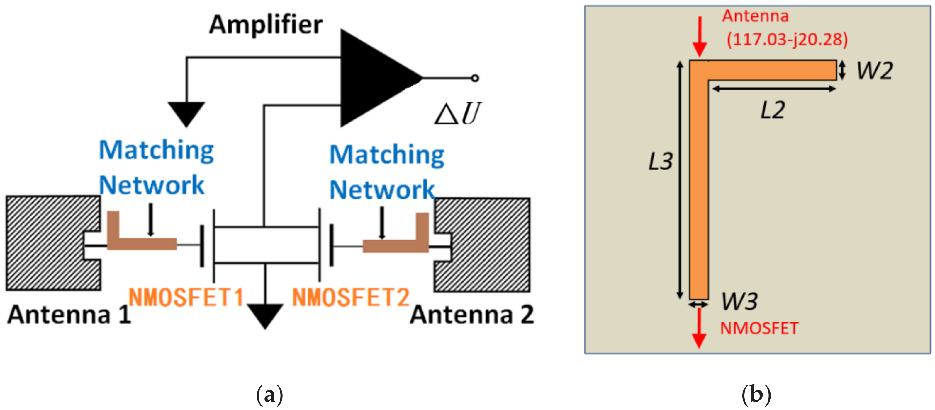
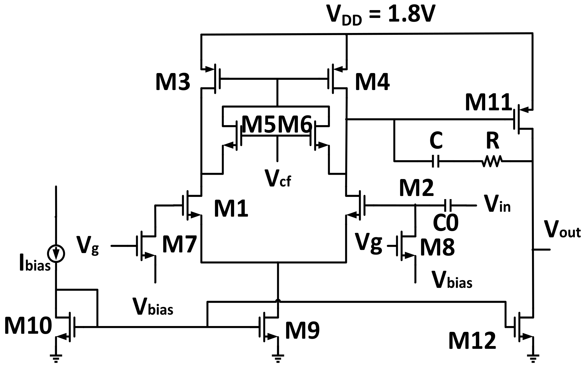
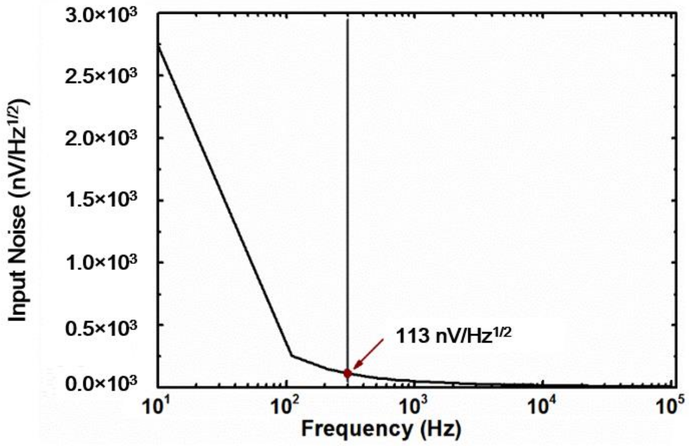
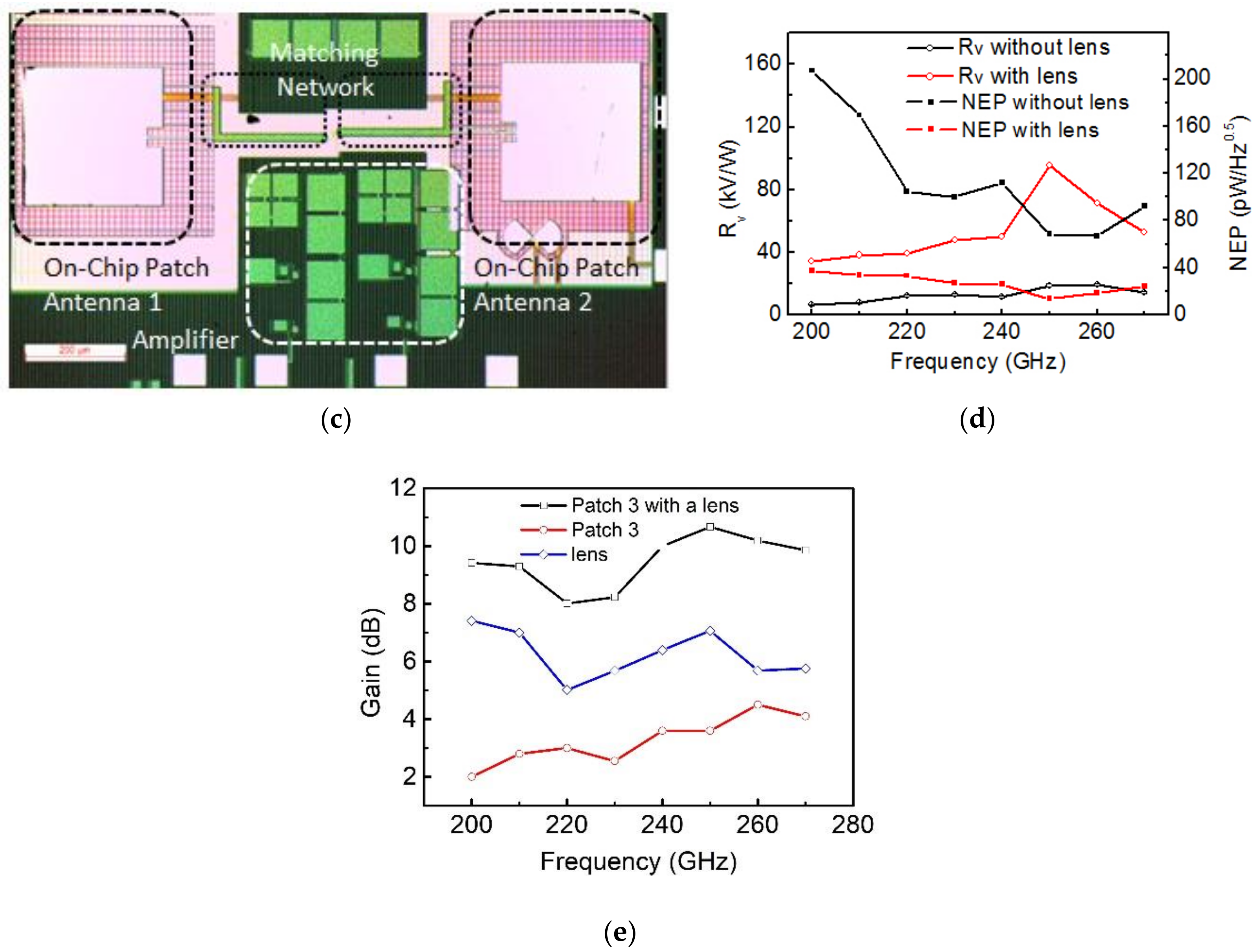
3. Terahertz Detector Circuit

Figure 3a shows the proposed detector structure. The antenna output port is connected to the matching network, and the network is connected to an NMOSFET (TeraFET) for improved power transfer efficiency. DC photoresponse ∆U of the on-chip amplifier output terminal was measured with an SR830 (Standard Research System, INC, Sunnyvale, CA, USA) lock-in amplifier which measured the ∆U amplitude submerged by noise at a determined frequency. Thus, the detector is thermal noise limited, and the detector also includes a dual antenna and dual NMOSFET (TeraFET) structure, which provides degree of noise suppression.
Antenna impedance is the ratio of input voltage to input current at the antenna feed. The best-case scenario is that antenna impedance is purely resistive and equal to half of the characteristic NMOSFET (TeraFET) impedance. There is no power reflection at the feeder terminal and no standing wave at the feed line, and antenna impedance changes slowly with frequency. Ideal matching will eliminate reactance. The NMOSFET’s characteristic resistive impedance can be adjusted by increasing the applied voltage for better performance. Impedance matching between the antenna and NMOSFET (TeraFET) was achieved using an L-type matching network comprising a microstrip open-stub and microstrip line section to reduce the imaginary part magnitude as much as possible through the matching network, as shown in Figure 3b. Selected section dimensions were L2 = 105 µm, W2 = 13.6 µm, L3 = 222 µm, and W3 = 13.36 µm.
Figure 4 shows the circuit diagram for the proposed readout amplifier, comprising two stages. Stage 1 uses a common-source structure with large differential NMOS input pair (M1 and M2), since increased size can reduce input-referred flicker noise. M3 and M4 are also large to similarly reduce any contribution to flicker noise. M5 and M6 operate in their linear region, acting as resistors to provide common-mode feedback. C0 is a 10 pF capacitor with larger equivalent resistance at low frequency. M8 must operate in the sub-threshold region to provide direct current bias for M1 and M2 to ensure that the alternating current signal passes through the capacitor to M2 and M7 gate.
Stage 2 uses a PMOS input device with a common-source single-ended structure. The R and C provide Miller compensation for circuit stability when operated as a closed loop.
The proposed on-chip low-noise amplifier (LNA) shown in Figure 4 compensates for low-gain antennas. Two key issues must be solved during circuit design, namely low-noise performance and amplification ability under low frequency. The amplifier, fabricated in the standard 0.18 µm CMOS process, provides 42 dB voltage gain and 4 MHz 3 dB bandwidth with capacitor feedback. Simulated input-referred noise is 17 nV/Hz1/2 at 10 kHz and 113 nV/Hz1/2 at 310 Hz. Amplifier power consumption is 3.5 mW with 1.8 V supply voltage. Figure 5 shows the input-referred noise curve.

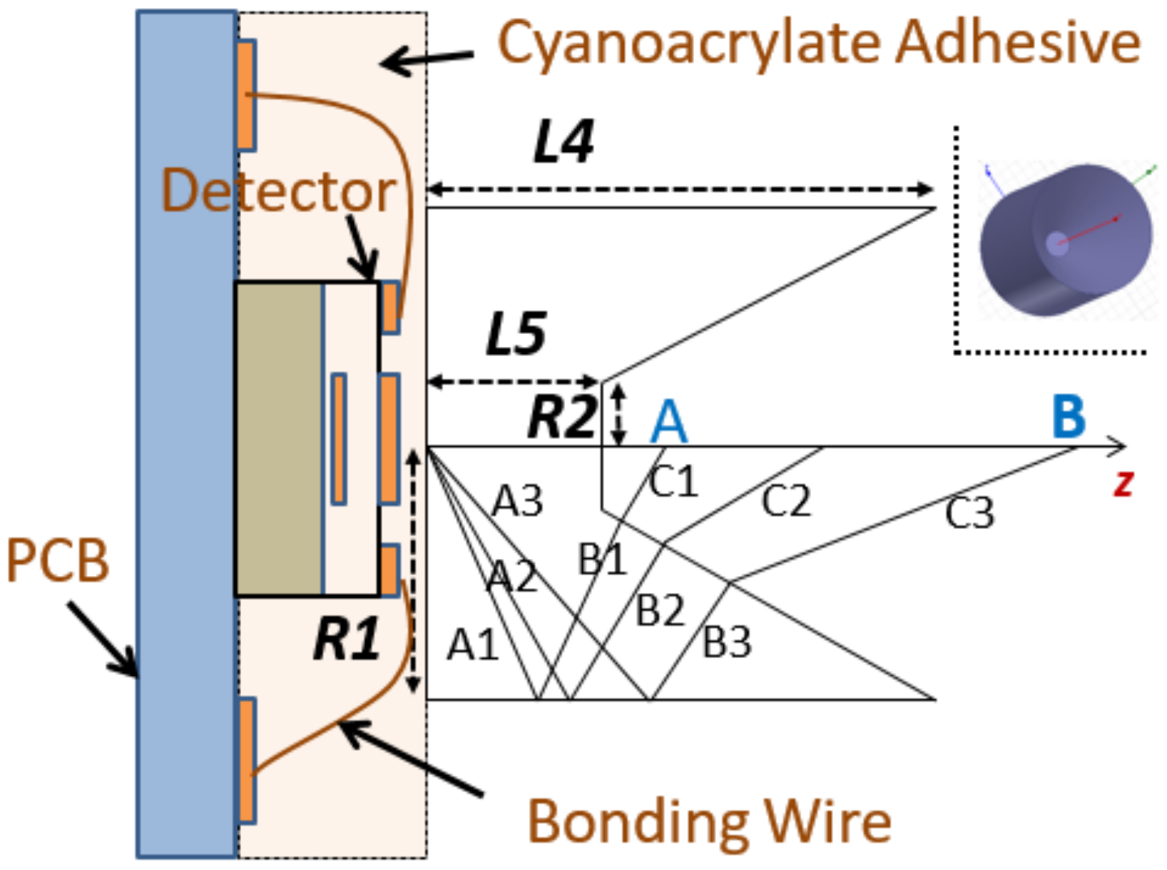
4. Catadioptric Horn-Like Lens

Traditional catadioptric optical systems are commonly used for optical telescopes, telephoto lenses, early lighthouse focusing systems, searchlights, etc., with refraction achieved by lenses and reflection by curved mirrors. This lens can be easily integrated with THz detectors in contrast with conventional quasi-optical components, as shown in Figure 6. Terahertz detector front-end antennas have been physically coupled to back-end silicon lens previously to yield a compact system [10]. Therefore, this study proposes a THz detector with front-end antenna and lens symmetric about the z-axis to reduce signal loss in the substrate.
Figure 7 shows a simulated lens, where the lens’ out-radius R1 = 3 mm and in-radius R2 = 0.6 mm (R1 is about ελ0, where λ0 is the free-space wavelength [29]). Catadioptric lens length L4 = 6 mm, corresponding to 2ελ0 at 270 GHz. Length between out-radius and in-radius L5 = 2 mm, approximately λ0. When A1, A2, and A3 rays radiate from the source, they are totally reflected at the reflection plane (B1, B2, and B3, respectively), which are then refracted at the refraction plane (C1, C2, and C3, respectively).
The THz wave power received by the antenna is proportional to the antenna area, hence the two antennas receive approximately twice the power as a single antenna. The signal is converted to a direct voltage signal by the detector. Although the two NMOSFETs (TeraFETs) are connected in parallel, the output voltage does not increase but the output current doubles. Since the equivalent impedance for the low-noise amplifier input is large, the output current is converted into a voltage, hence doubling the voltage signal after passing through the low-noise amplifier.
Figure 6 and Figure 7 show that the refracted rays are distributed and converged to the z-axis, and the distribution provides up to 17.14 dB total gain, considerably higher than that achieved without the lens. The catadioptric dielectric lens is easily fabricated and illuminated compared with a silicon lens [10]. Figure 8 shows S11, gain, and efficiency with respect to frequency, where Port 1 is shown in Figure 2. Figure 9b shows that the catadioptric dielectric lens also increases antenna impedance.

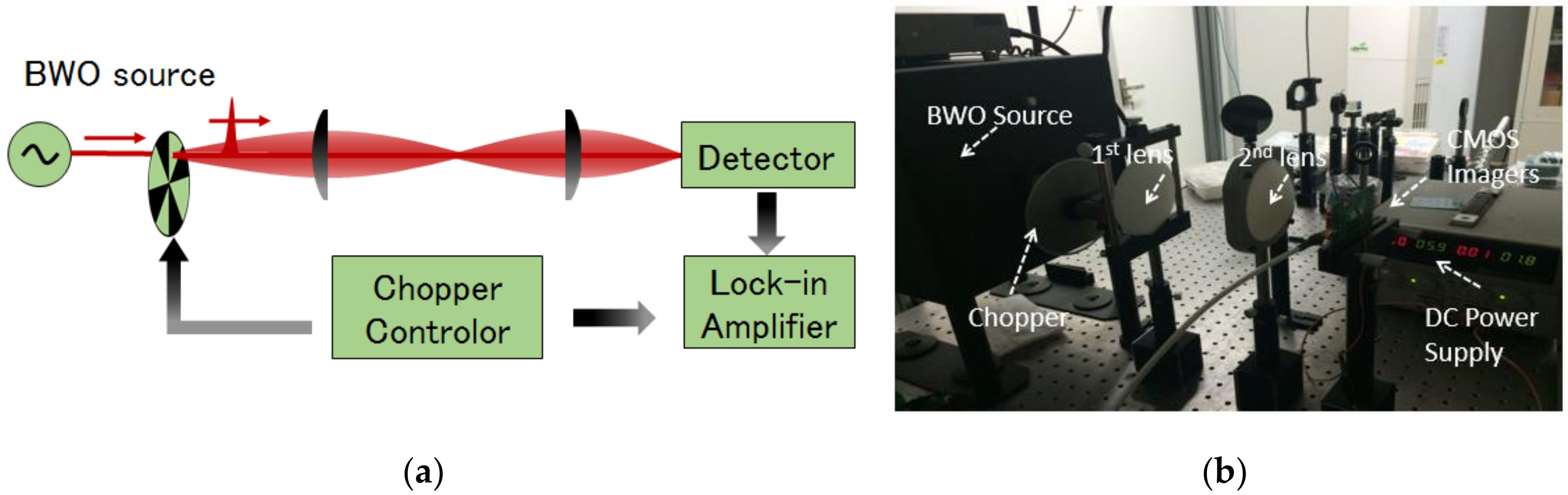
5. Terahertz Chip Measurements

The THz detector performance was modelled using Dyakonov–Shur plasma wave theory. Plasma waves at the insulator–metal interface can not only achieve THz wave detection but also achieve power amplification [11,30], where ∆U is the measured voltage from the SR830 at the amplifier output terminal, as shown in Figure 3a [31], and there is a positive correlation between ∆U and received power. Plasma waves are usually overdamped in CMOS structures [32,33], hence we propose a non-resonant broadband detector [34].
The method in [31] was used to determine voltage responsivity RV for a detector as follows:
R V = Δ U P d e t = 0 L E ( x ) d x L T H z A d e t
where Pdet is the THz power received by antennas, L is the length of the NMOSFET (TeraFET); E is the electric field intensity caused by terahertz waves, LTHz is the THz power density on the antennas measured with a large aperture THz power meter [31,33,35,36], as shown in Table 3, and Adet ≈ 0.075 mm2 is the rectangular inset-feed patch antenna size:
G A = Δ U G T λ 4 π R 2 R V P B W O
following [21], where GT is the total gain due to the first and second lenses, and on-chip and lock-in amplifiers, as shown in Figure 10b, R = 40 cm is the distance between the backward wave oscillator (BWO) and detector, PBWO is the power of the BWO wave source [21], as shown in Table 3, and λ is the wavelength. By adjusting the position of the lenses and the THz power meter, the THz power meter position of maximum LTHz is recorded, then the THz power meter is replaced with detector chip.
The gain of the horn-like lens is as follows:
G L = R V w i t h   l e n s   R V w i t h o u t   l e n s
NMOSFET channel thermal noise is the dominant noise source for a non-current biased NMOSFET detector. Noise equivalent power (NEP) determines the detector noise component with respect to the particular wavelength and measurement bandwidth, and represents the minimum optical power required for output signal-to-noise ratio = 1 [37]. Since the on-chip amplifier and detector are integrated on the same chip, low-noise amplifier noise cannot be measured separately. However, simulation shows low-noise amplifier NEP to be very small, hence amplifier flicker noise was negligible and need not be considered. Therefore, we estimated the detector NEP as follows:
N E P = 4 k T R d s / R V
where k is the Boltzmann constant, T is the measurement environment temperature (nominally 300 K), and Rds is half of the drain-source resistance.
The NMOSFET threshold voltage was approximately 0.45 V. The detectors were tested with gate voltages from 0.15 V to 0.36 V and bias voltage = 0.238 V for maximum RV. The NMOSFET is most suitable to operate in the sub-threshold region, forming a two-dimensional electronic fluid, increasing channel resistance sufficiently, and most likely to obtain maximum RV.
Figure 10e shows that the detector with catadioptric dielectric lens achieved RV = 95.67 kV/W with NEP = 12.8 pW/Hz0.5 at 250 GHz, whereas it achieved RV = 19.2 kV/W with NEP = 67.2 pW/Hz0.5 at 260 GHz without the lens. Comparing Figure 10d with Figure 8, simulated frequencies for maximum RV differed from the measured case. The most likely cause was fabrication error. Figure 10e shows patch antenna gain with and without catadioptric lens calculated from Equations (6)–(8). GA is relatively meaningless due to the on-chip and lock-in amplifiers, but GL is accurate. Patch antenna gain with a catadioptric lens was slightly lower than the simulation result.

6. Conclusions

This study proposed a THz rectangular inset-feed patch antenna that can be easily achieved in CMOS technology and can be integrated perfectly with a low-noise amplifier. However, the antenna has narrow bandwidth and is sensitive to dielectric constant and shape. The dielectric constant cannot be changed by the circuit and antenna designer for standard CMOS processing, but antenna impedances and operating frequency can be controlled by reasonable on-chip antenna design considering antenna gain and bandwidth. A front-end ZEONEX RS420 catadioptric horn-like lens greatly improved voltage responsivity of the THz detector.
Two patch antennas with lens achieved 17.14 dB maximum simulated gain at 267 GHz, while the gain of two patch antennas is 4.5 dB at 260 GHz and the gain of two antennas with catadioptric lens is 10.67 dB at 250 GHz.

Author Contributions

Methodology, Investigation, Writing—original draft, and Data curation, F.Z.; Conceptualization, Supervision, and Project administration, L.M.; Resources, W.G.; Funding acquisition, S.X.; Writing—review and editing, C.A.T.H.T. All authors have read and agreed to the published version of the manuscript.

Funding

This work was supported by the National Natural Science Foundation of China (Grant No. 51425502) and the Tianjin Natural Science Foundation (Grant Nos. 18JCQNJC04800 and 18JCZDJC31800).

Acknowledgments

The authors wish to thank Cunlin Zhang, Physics Department, Capital Normal University, Beijing, China, for providing a THz BWO source to measure the detector.

Conflicts of Interest

The authors declare no conflict of interest.

References

  1. Liu, Z.-Y.; Qi, F.; Wang, Y.-L.; Liu, P.-X.; Li, W.-F. A 220- to 299-GHz CMOS Terahertz Detector. J. Infrared Millim. Terahertz Waves 2019, 40, 606–619. [Google Scholar] [CrossRef]
  2. Choe, W.; Jeong, J. A Broadband THz On-Chip Transition Using a Dipole Antenna with Integrated Balun. Electronics 2018, 7, 236. [Google Scholar] [CrossRef] [Green Version]
  3. Zheng, Y.; Song, L.; Huang, J.; Zhang, H.; Fang, F. Detection of the three-dimensional trajectory of an object based on a curved bionic compound eye. Opt. Lett. 2019, 44, 4143–4146. [Google Scholar] [CrossRef] [PubMed]
  4. Peng, B.; Lei, J.; Fu, H.; Zhang, C.; Chua, T.-S.; Li, X. Unsupervised Video Action Clustering via Motion-Scene Interaction Constraint. IEEE Trans. Circuits Syst. Video Technol. 2020, 30, 131–144. [Google Scholar] [CrossRef]
  5. Preu, S. Introduction to the Special Issue on Terahertz Cameras and Detector Arrays. J. Infrared Millim. Terahertz Waves 2015, 36, 877–878. [Google Scholar] [CrossRef] [Green Version]
  6. Shanawani, M.; Masotti, D.; Costanzo, A. THz Rectennas and Their Design Rules. Electronics 2017, 6, 99. [Google Scholar] [CrossRef] [Green Version]
  7. Bauer, M.; Raemer, A.; Chevtchenko, S.A.; Osipov, K.Y.; Cibiraite, D.; Pralgauskaite, S.; Ikamas, K.; Lisauskas, A.; Heinrich, W.; Krozer, V.; et al. A High-Sensitivity AlGaN/GaN HEMT Terahertz Detector With Integrated Broadband Bow-Tie Antenna. IEEE Trans. Terahertz Sci. Technol. 2019, 9, 430–444. [Google Scholar] [CrossRef]
  8. Zak, A.; Andersson, M.A.; Bauer, M.; Matukas, J.; Lisauskas, A.; Roskos, H.G.; Stake, J. Antenna-Integrated 0.6 THz FET Direct Detectors Based on CVD Graphene. Nano Lett. 2014, 14, 5834–5838. [Google Scholar] [CrossRef]
  9. Qin, H.; Li, X.; Sun, J.; Zhang, Z.; Sun, Y.; Yu, Y.; Li, X.; Luo, M. Detection of incoherent terahertz light using antenna-coupled high-electron-mobility field-effect transistors. Appl. Phys. Lett. 2017, 110, 171109. [Google Scholar] [CrossRef] [Green Version]
  10. Hadi, R.A.; Sherry, H.; Grzyb, J.; Baktash, N.; Zhao, Y.; Öjefors, E.; Kaiser, A.; Cathelin, A.; Pfeiffer, U. A broadband 0.6 to 1 THz CMOS imaging detector with an integrated lens. In Proceedings of the 2011 IEEE MTT-S International Microwave Symposium, Baltimore, MD, USA, 5–10 June 2011. [Google Scholar]
  11. Zhao, F.; Zhu, C.; Guo, W.; Cong, J.; Tee, C.A.T.H.; Song, L.; Zheng, Y. Resonant Tunneling Diode (RTD) Terahertz Active Transmission Line Oscillator with Graphene-Plasma Wave and Two Graphene Antennas. Electronics 2019, 8, 1164. [Google Scholar] [CrossRef] [Green Version]
  12. Zhao, F.; Wang, Y.; Guo, W.; Cong, J.; Tee, C.A.T.; Song, L.; Zheng, Y. Analysis of the eight parameter variation of the resonant tunneling diode (RTD) in the rapid thermal annealing process with resistance compensation effect. AIP Adv. 2020, 10, 035103. [Google Scholar] [CrossRef] [Green Version]
  13. Ojefors, E.; Pfeiffer, U.R.; Lisauskas, A.; Roskos, H.G. A 0.65 THz Focal-Plane Array in a Quarter-Micron CMOS Process Technology. IEEE J. Solid State Circuits 2009, 44, 1968–1976. [Google Scholar] [CrossRef]
  14. Han, R.; Zhang, Y.; Coquillat, D.; Hoy, J.; Videlier, H.; Knap, W.; Brown, E.; Kenneth, K.O. A 280-GHz schottky diode detector in 130-nm digital CMOS. IEEE J. Solid State Circuits 2011, 46, 2602–2612. [Google Scholar] [CrossRef]
  15. Uzunkol, M.; Gurbuz, O.D.; Golcuk, F.; Rebeiz, G.M. A 0.32 THz SiGe 4x4 Imaging Array Using High-Efficiency On-Chip Antennas. IEEE J. Solid State Circuits 2013, 48, 2056–2066. [Google Scholar] [CrossRef]
  16. Yang, S.Y.; Cho, C.S.; Lee, J.W.; Kim, J. Design of Sub-THz Log-Periodic Antenna for High Input Impedance. In Proceedings of the 34th International Conference on Infrared, Millimeter, and Terahertz Waves, Busan, Korea, 21–25 September 2009; pp. 739–740. [Google Scholar]
  17. Wang, P.; Huang, Y.H.; Zuo, Z.G.; Yu, J.Z. Optimization of 0.34 THz log-periodic antenna for superconducting terahertz emitter. In Proceedings of the 2015 Asia-Pacific Microwave Conference (APMC), Nanjing, China, 6–9 December 2015; pp. 1–5. [Google Scholar]
  18. Seok, E.; Cao, C.; Shim, D.; Arenas, D.J. A 410GHz CMOS Push-Push Oscillator with an On-Chip Patch Antenna. In Proceedings of the 2008 IEEE International Solid-State Circuits Conference, San Francisco, CA, USA, 3–7 February 2008; pp. 472–629. [Google Scholar]
  19. Boppel, S.; Lisauskas, A.; Bauer, M.; Hajo, A.S.; Zdanevičius, J.; Matukas, J.; Mittendorff, M.; Winnerl, S.; Krozer, V.; Roskos, H.G. Monolithically-integrated antenna-coupled field-effect transistors for detection above 2 THz. In Proceedings of the European Conference on Antennas and Propagation, Lisbon, Portugal, 13–17 April 2015; pp. 1–3. [Google Scholar]
  20. Xu, L.J.; Tong, F.C.; Xue, B.; Qin, L. Design of miniaturised on-chip slot antenna for THz detector in CMOS. IET Microw. Antennas Propag. 2018, 12, 1324–1331. [Google Scholar] [CrossRef]
  21. Li, C.H.; Chiu, T.Y. 340-GHz Low-Cost and High-Gain On-Chip Higher Order Mode Dielectric Resonator Antenna for THz Applications. IEEE Trans. Terahertz Sci. Technol. 2017, 7, 284–294. [Google Scholar] [CrossRef]
  22. Grzyb, J.; Zhao, Y.; Pfeiffer, U.R. A 288-GHz Lens-Integrated Balanced Triple-Push Source in a 65-nm CMOS Technology. IEEE J. Solid State Circuits 2013, 48, 1751–1761. [Google Scholar] [CrossRef]
  23. Cong, J.; Mao, L.; Xie, S.; Zhao, F.; Yan, D.; Guo, W. Photoelectric Dual Control Negative Differential Resistance Device Fabricated by Standard CMOS Process. IEEE Photonics J. 2019, 11, 1–11. [Google Scholar] [CrossRef]
  24. Niu, K.; Huang, Z.; Li, M.; Wu, X. Optimization of the Artificially Anisotropic Parameters in WCS-FDTD Method for Reducing Numerical Dispersion. IEEE Trans. Antennas Propag. 2017, 65, 7389–7394. [Google Scholar] [CrossRef]
  25. Harrington, R.F. Time-Harmonic Electromagnetic Fields. Siam J. Math. Anal. 1961, 12, 323. [Google Scholar]
  26. Schneider, M.V. Microstrip Lines for Microwave Integrated Circuits. Bell Labs Tech. J. 1969, 48, 1421–1444. [Google Scholar] [CrossRef]
  27. Jameson, S.; Halpern, E.; Socher, E. A 300 GHz wirelessly locked 2*3 array radiating 5.4 dBm with 5.1% DC-to-RF efficiency in 65 nm CMOS. In Proceedings of the 2016 IEEE International Solid-State Circuits Conference, San Francisco, CA, USA, 31 January–4 February 2016; pp. 348–349. [Google Scholar]
  28. Golcuk, F.; Gurbuz, O.D.; Rebeiz, G.M. A 0.39–0.44 THz 2x4 Amplifier-Quadrupler Array With Peak EIRP of 3–4 dBm. IEEE Trans. Microw. Theory Tech. 2013, 61, 4483–4491. [Google Scholar] [CrossRef]
  29. Banik, B. Photonic THz Generation and Quasioptical Integration for Imaging Applications; Chalmers University of Technology: Goteborg, Sweden, 2009. [Google Scholar]
  30. Yu, A.Q.; Guo, X.G.; Zhu, Y.M.; Balakin, A.V.; Shkurinov, A.P. Metal-graphene hybridized plasmon induced transparency in the terahertz frequencies. Opt. Express 2019, 27, 11. [Google Scholar] [CrossRef] [PubMed]
  31. Schuster, F.; Coquillat, D.; Videlier, H.; Sakowicz, M.; Teppe, F.; Dussopt, L.; Giffard, B.; Skotnicki, T.; Knap, W. Broadband terahertz imaging with highly sensitive silicon CMOS detectors. Opt. Express 2011, 19, 7827–7832. [Google Scholar] [CrossRef]
  32. Knap, W.; Dyakonov, M.; Coquillat, D.; Teppe, F.; Dyakonova, N.; Lusakowski, J.; Karpierz, K.; Sakowicz, M.; Valusis, G.; Seliuta, D.; et al. Field Effect Transistors for Terahertz Detection: Physics and First Imaging Applications. J. Infrared Millim. Terahertz Waves 2009, 30, 1319–1337. [Google Scholar] [CrossRef] [Green Version]
  33. Lisauskas, A.; Roskos, H.G. Terahertz imaging with Si MOSFET focal-plane arrays. Proc. SPIE Int. Soc. Opt. Eng. 2009, 7215, 935–937. [Google Scholar] [CrossRef]
  34. Dyakonov, M.; Shur, M. Shallow water analogy for a ballistic field effect transistor: New mechanism of plasma wave generation by dc current. Phys. Rev. Lett. 1993, 71, 2465. [Google Scholar] [CrossRef]
  35. Lisauskas, A.; Pfeiffer, U.; Oejefors, E.; Bolivar, P.H.; Glaab, D.; Roskos, H.G. Rational design of high-responsivity detectors of terahertz radiation based on distributed self-mixing in silicon field-effect transistors. J. Appl. Phys. 2009, 105, 114511. [Google Scholar] [CrossRef]
  36. Sherry, H.; Hadi, R.A.; Grzyb, J.; Öjefors, E.; Cathelin, A.; Kaiser, A.; Pfeiffer, U.R. Lens-integrated THz imaging arrays in 65 nm CMOS technologies. In Proceedings of the 2011 IEEE Radio Frequency Integrated Circuits Symposium, Baltimore, MD, USA, 5–7 June 2011; pp. 1–4. [Google Scholar]
  37. Zheng, Y.; Song, L.; Hu, G.; Zhao, M.; Tian, Y.; Zhang, Z.; Fang, F. Improving environmental noise suppression for micronewton force sensing based on electrostatic by injecting air damping. Rev. Sci. Instrum. 2014, 85, 055002. [Google Scholar] [CrossRef]
Figure 1. Cross-sectional view for the proposed United Microelectronics Corporation (UMC) 0.18 μm CMOS design.
Electronics 09 01049 g001
Figure 2. Structures for the proposed on-chip patch antenna.
Electronics 09 01049 g002
Figure 3. (a) MOSFET detector structure and (b) matching network between on-chip antenna and NMOSFET.
Electronics 09 01049 g003
Figure 4. Proposed low-noise amplifier (LNA).
Electronics 09 01049 g004
Figure 5. Low-noise amplifier (LNA)’s input-referred noise.
Electronics 09 01049 g005
Figure 6. Cross-sectional view for the proposed catadioptric lens with inset 3D view of the lens.
Electronics 09 01049 g006
Figure 7. Simulated gain at 280 GHz (a,b) individual patch antenna, (c,d) two patch antennas working together, and (e,f) two patch antennas with catadioptric lens. Red and brown lines represent 2D simulated radiation pattern along Phi = 0° and 90° planes, respectively.
Electronics 09 01049 g007aElectronics 09 01049 g007b
Figure 8. Simulation results for (a) S11, (b) gain, and (c) efficiency.
Electronics 09 01049 g008
Figure 9. Output impedance: (a) patch antenna and (b) two patch antennas with catadioptric lens.
Electronics 09 01049 g009
Figure 10. (a) Measurement setup for the detectors, (b) micro-photo of the chip, (c) detector test platform, (d) RV and NEP, and (e) gain.
Electronics 09 01049 g010aElectronics 09 01049 g010b
Table 1. Proposed on-chip rectangular inset-feed patch antenna dimensions and performances [14].
ParameterPatch
Wg (µm)500
Lg (µm)500
W (µm)275
L (µm)275
Win (µm)90
Lin (µm)65
W1 (µm)5.5
L1 (µm)122
Gain (dB)6.89
Bandwidth (GHz)1.5
Central frequency (GHz)271
Radiation efficiency89.4%
Table 2. Performance comparison.
Ref.ProcessAntennaCenter Frequency
(GHz)
Gain
(dB)
Bandwidth (GHz)
[27]TSMC 65 nm CMOSRing2964.2-
[28]45 nm CMOS SOISlot ring3751.63
[21]0.18 µm CMOSRectangle + DRA3277.92.5
[20]TSMC 0.18 μm CMOSRectangle300–2.14.1
Circular3005.3011.3
Diamond3005.949.6
[14]0.18 μm CMOSRectangle284–17
[22]65 nm CMOSRing with silicon lens28818.3-
This workUMC 0.18 µm CMOSRectangle2716.891.5
Table 3. NMOSFET test results.
Frequency (GHz)PBWO
(mW)
LTHz
(mW/mm2)
∆U without Lens
(µV)
∆U with Lens
(µV)
2001221346.6540.8
2101424057.1707.4
220613392.3402
23022696.793.1
2404678.6246.85
25010160141.31148.04
26016267144.31338
27010187105.4749

