A 920-MHz Dual-Mode Receiver with Energy Harvesting for UHF RFID Tag and IoT †


Abstract
:1. Introduction
2. Proposed UHF RFID System
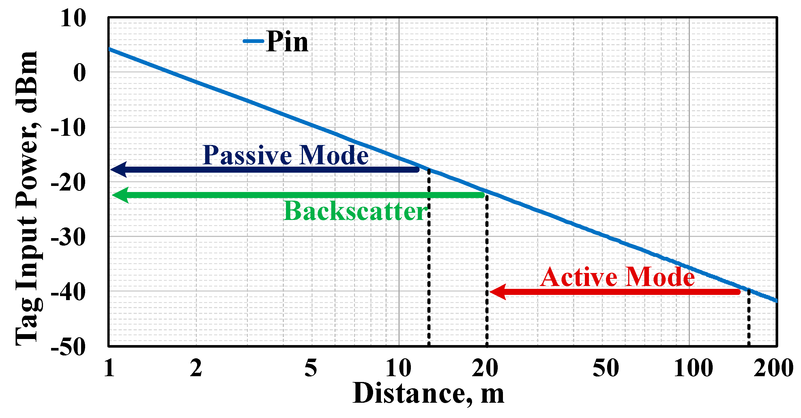
2.1. Link Budget
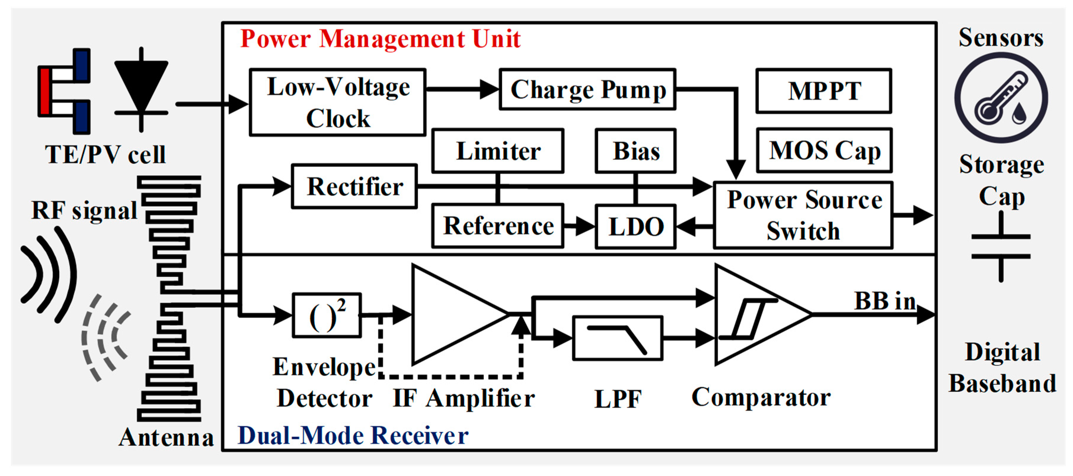
2.2. Architecture of RFID Tag
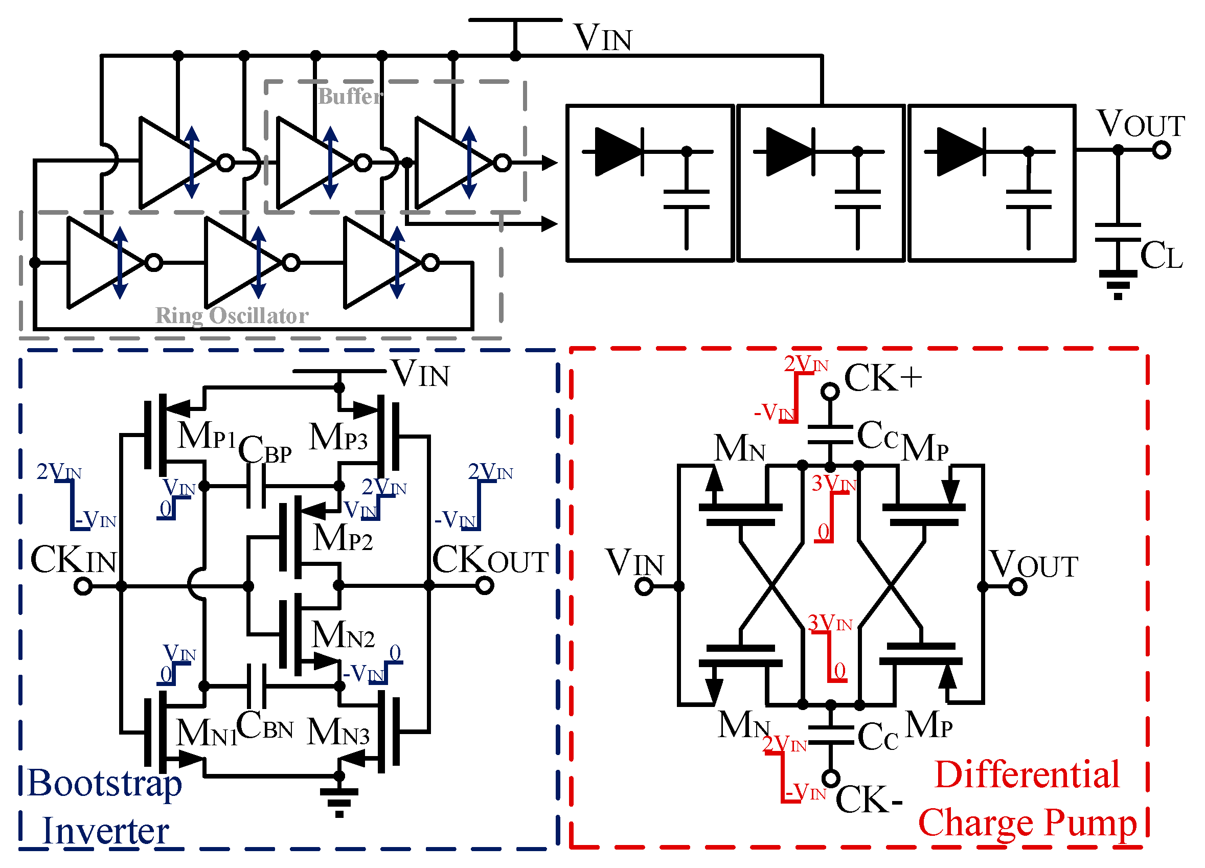
3. Proposed Energy Harvesting Topology
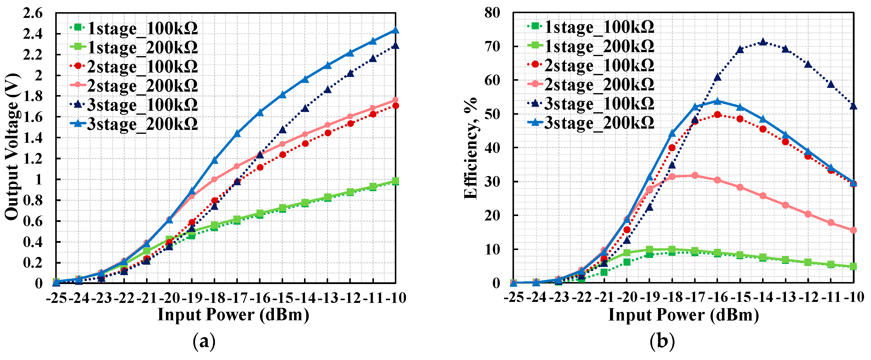
3.1. Photovoltaic and Thermoelectric Energy Harvesting
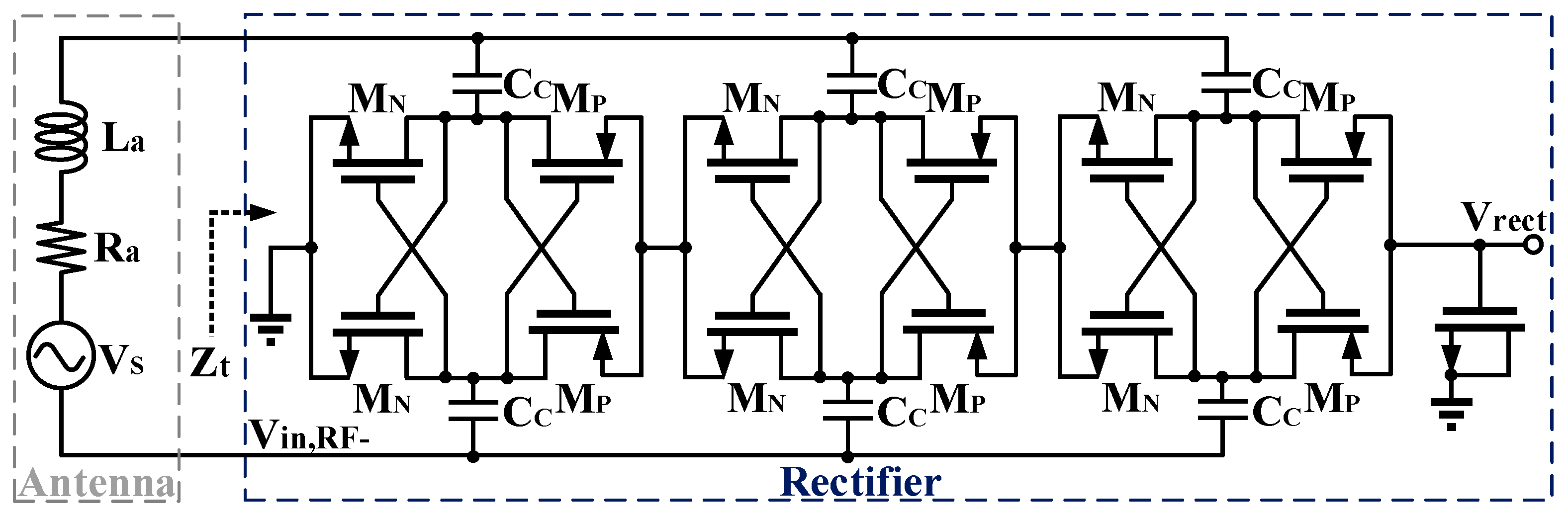
3.2. RF Energy Harvesting
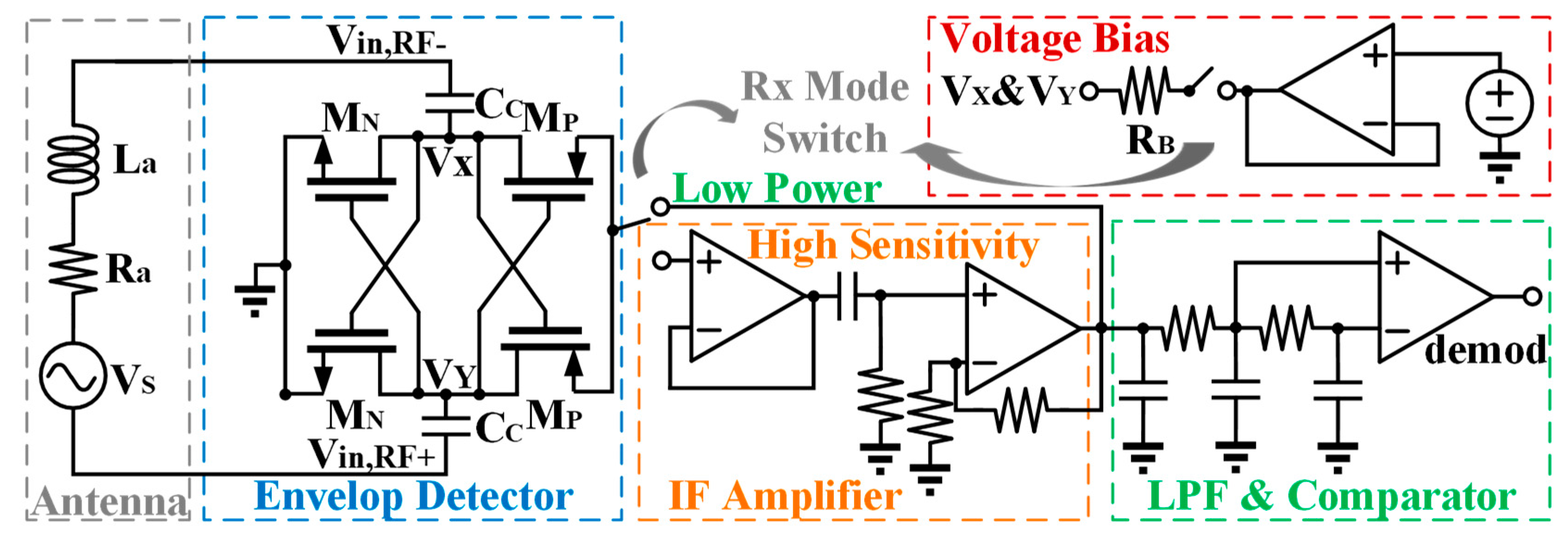
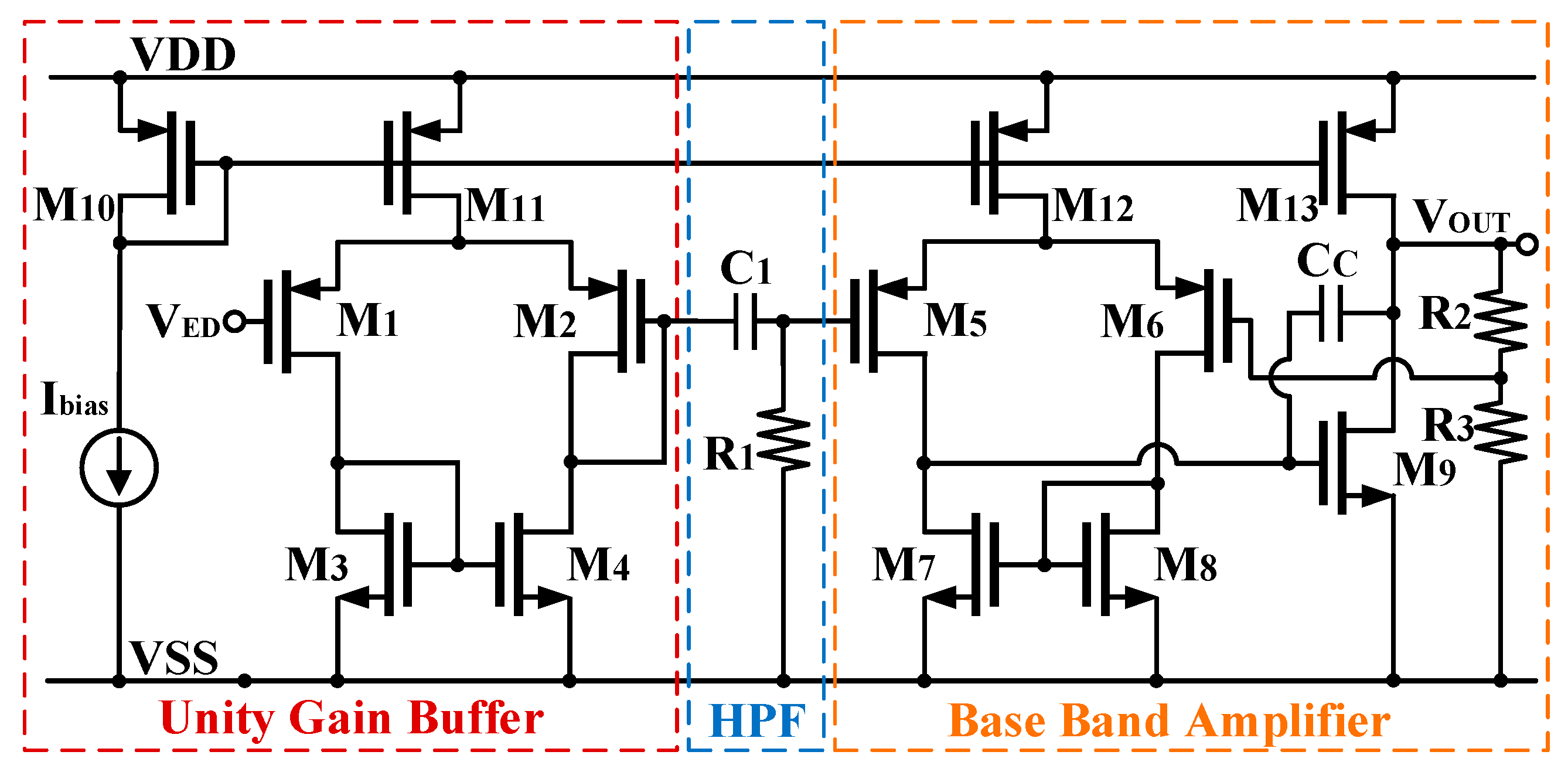
4. Proposed Dual-Mode Receiver
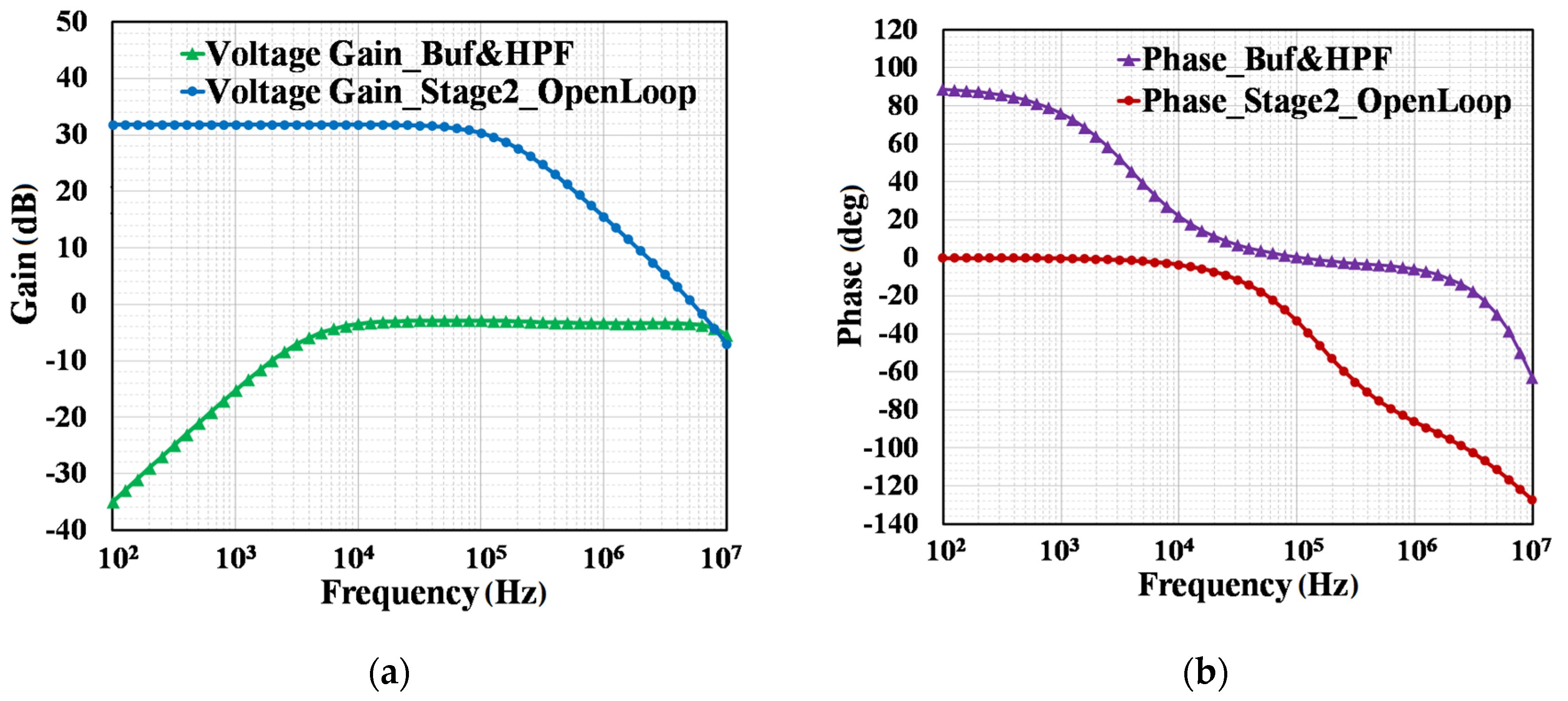
4.1. Architecture of Proposed Dual-Mode Receiver
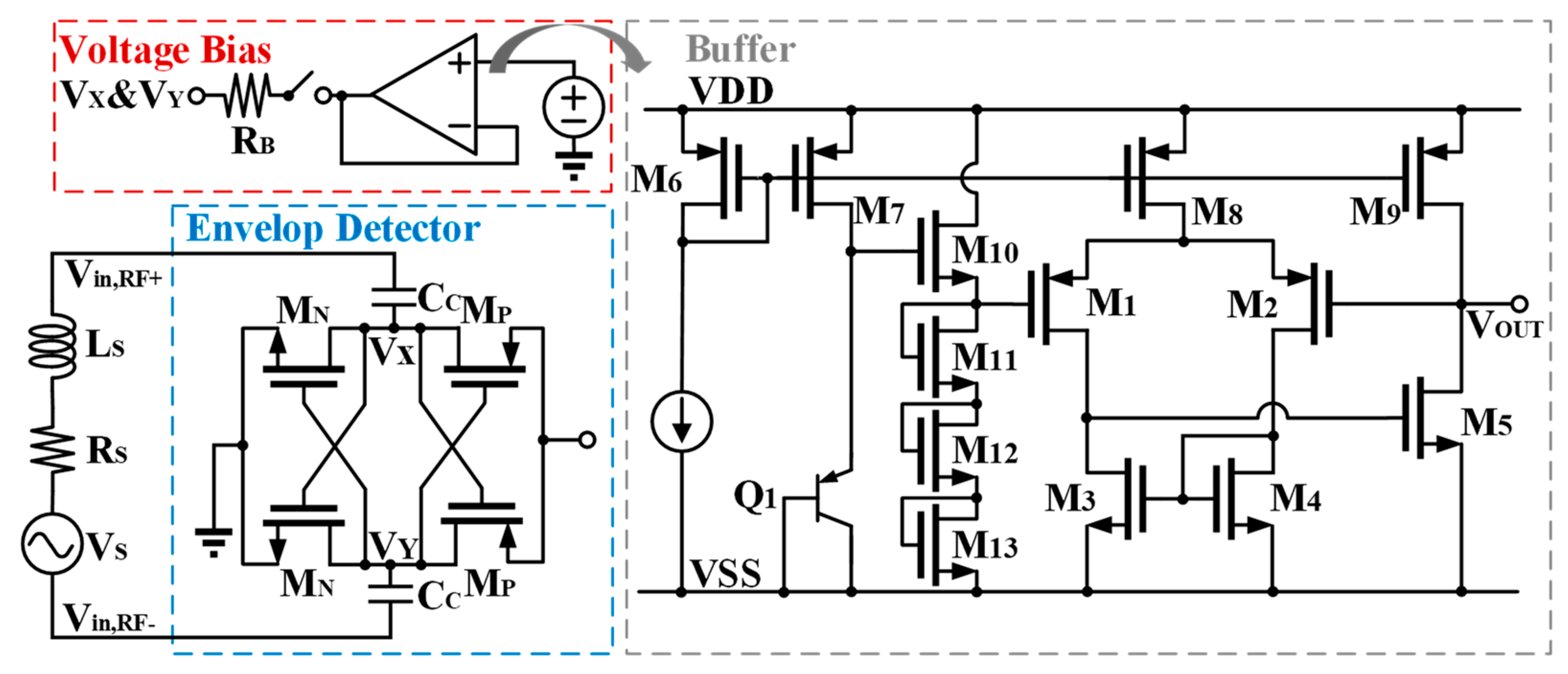
4.2. Envelop Detector with Voltage Bias
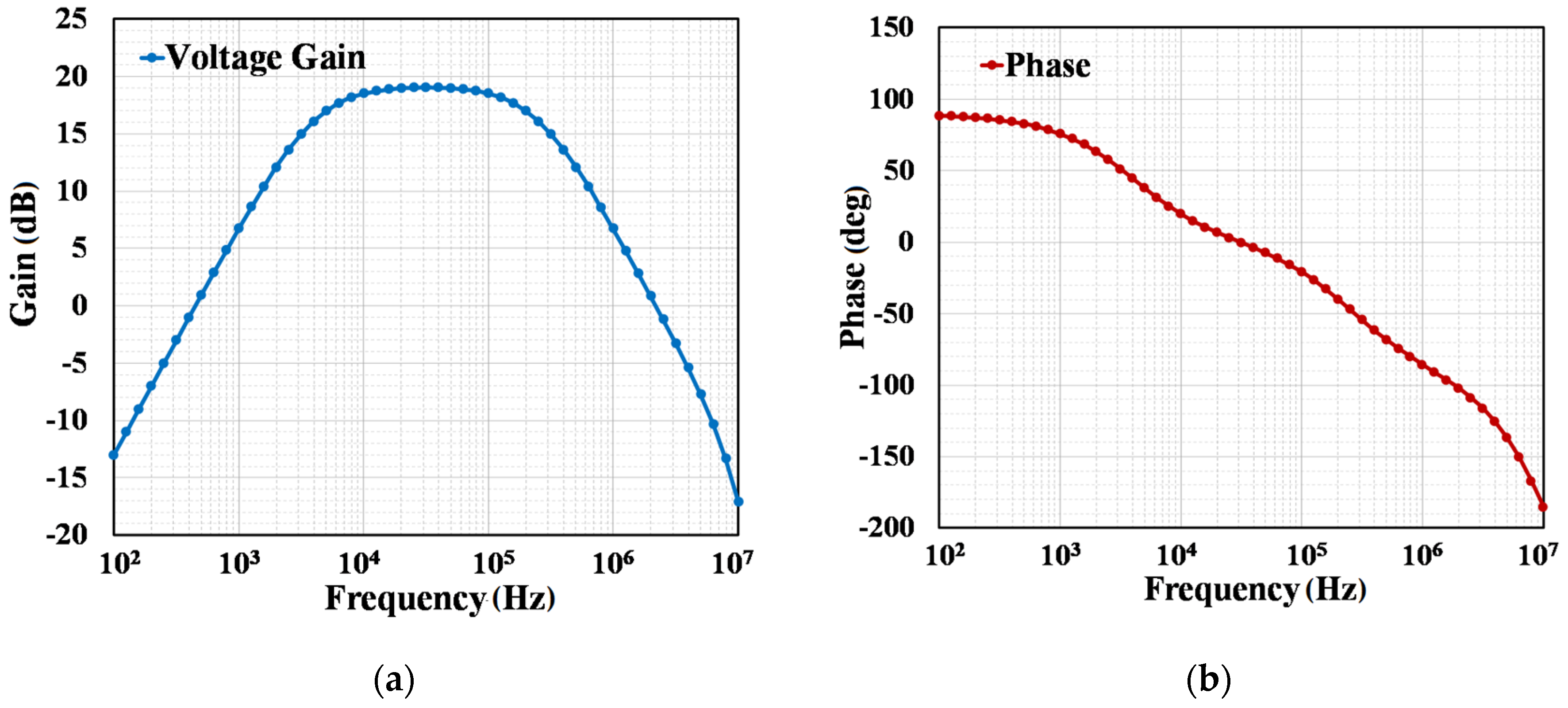
4.3. IF Amplifier
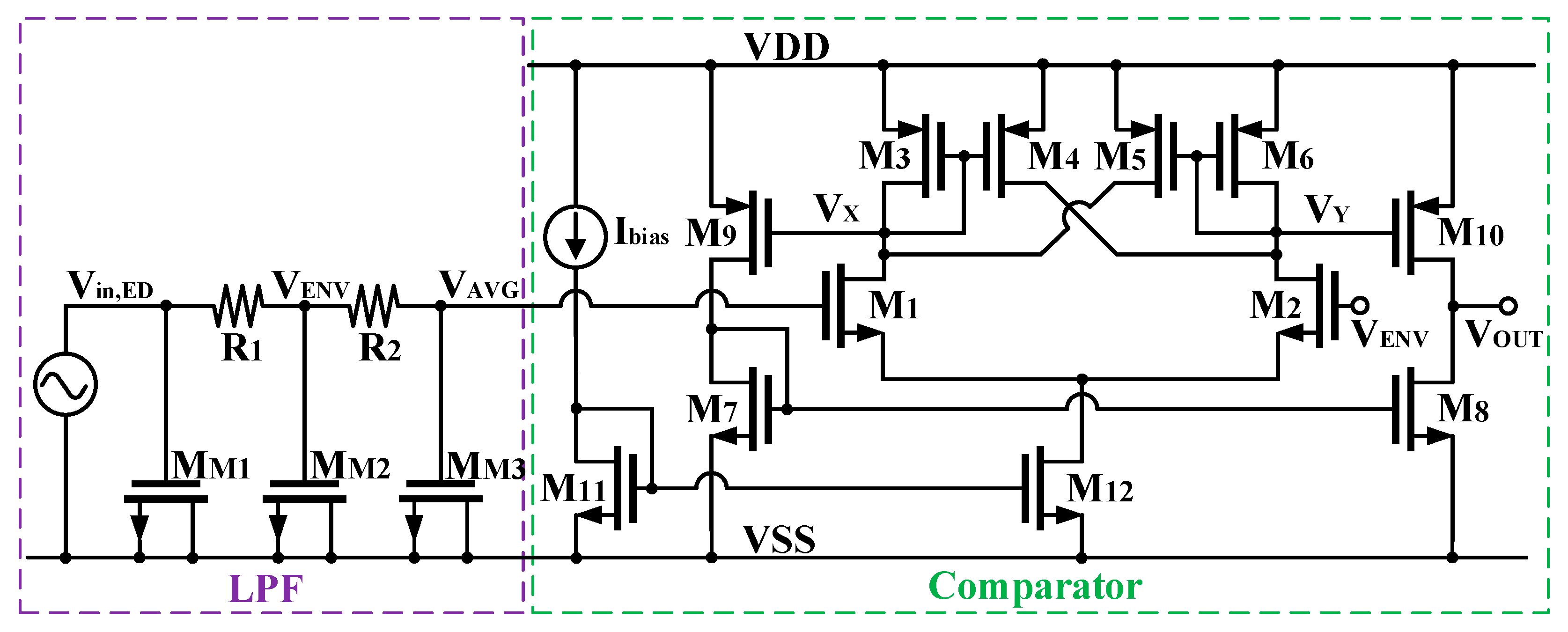
4.4. Demodulator
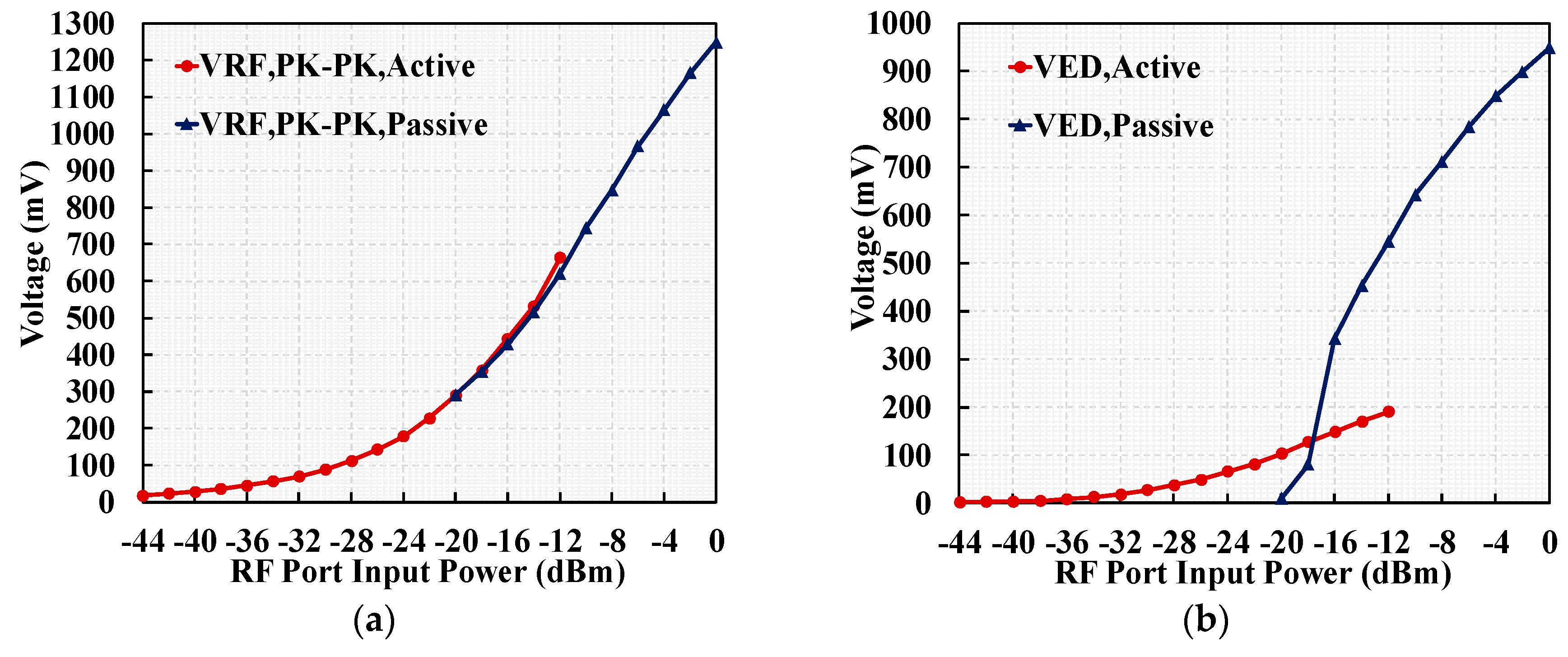
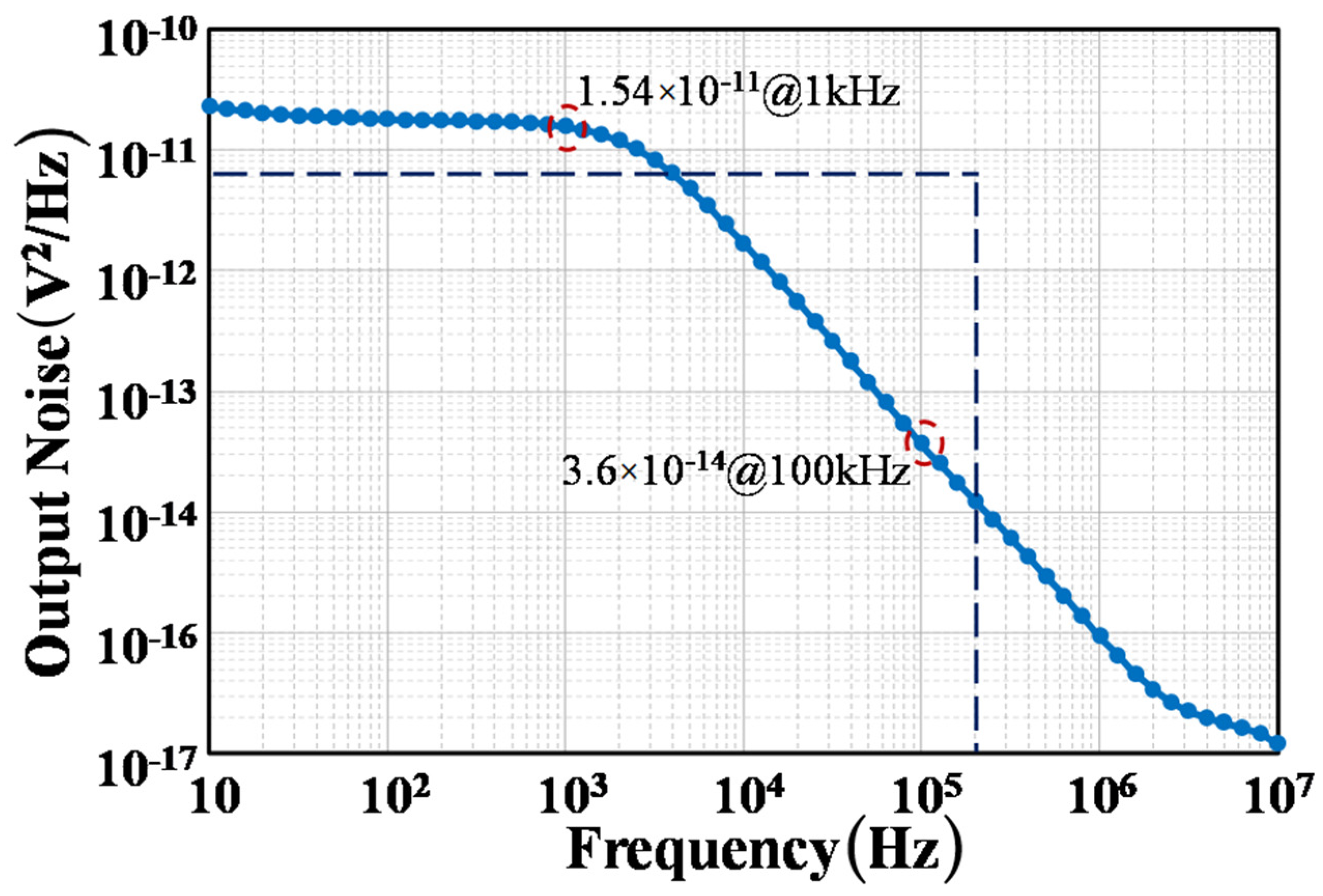
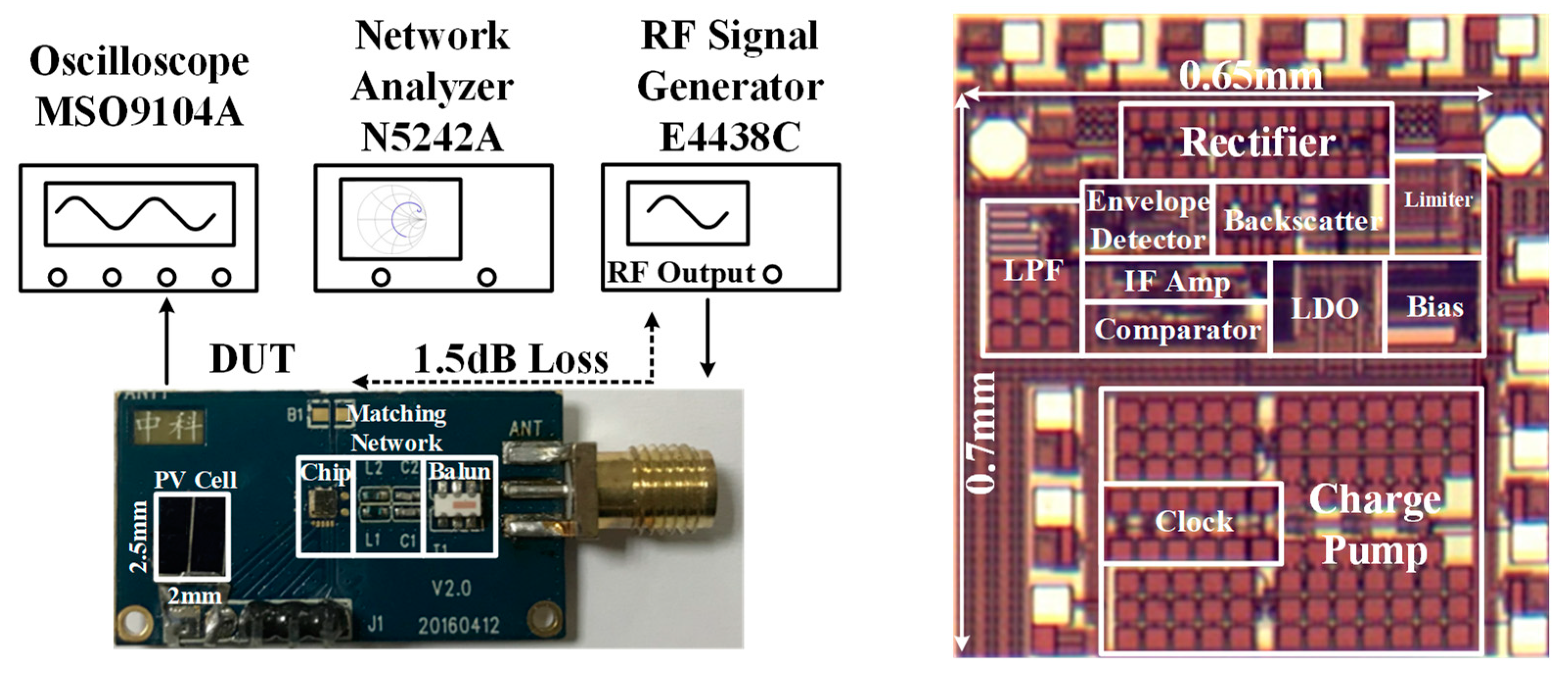
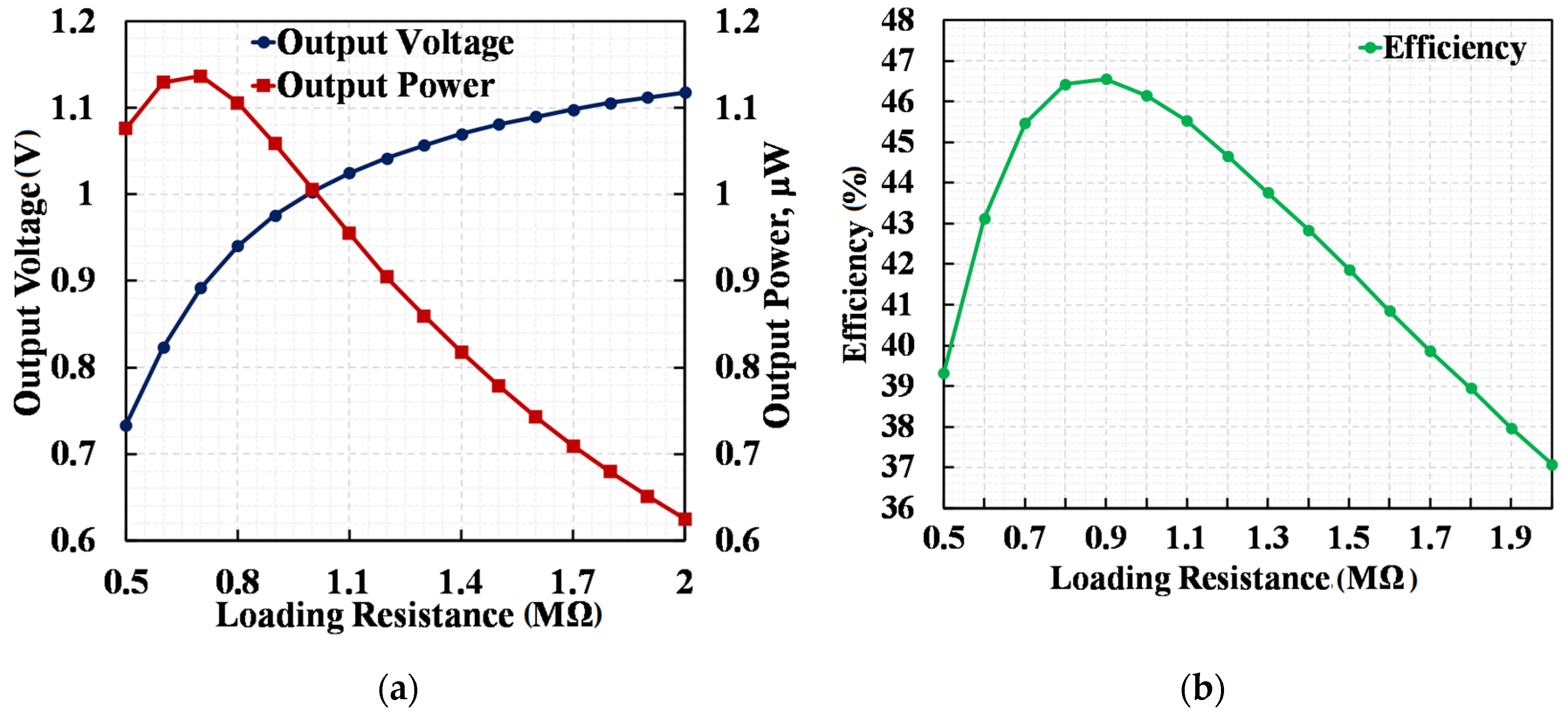
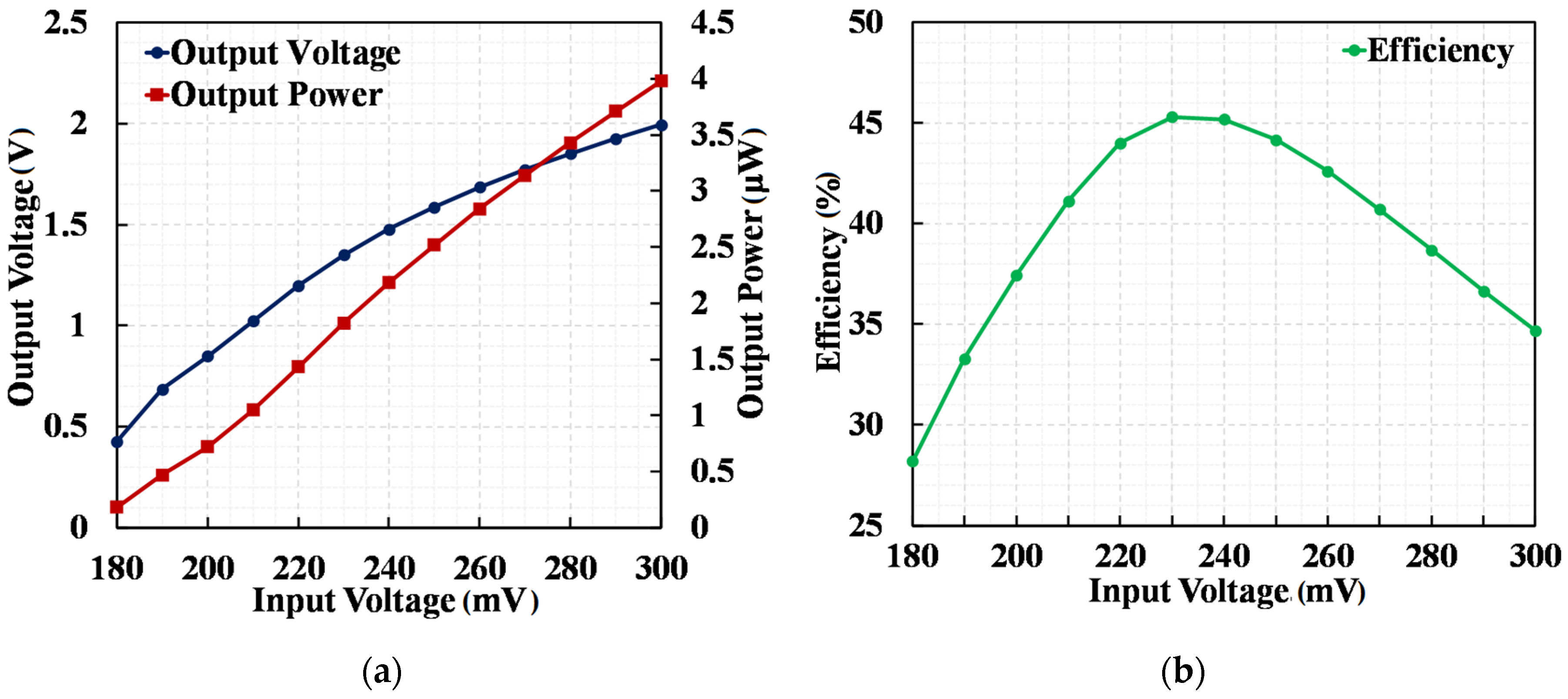
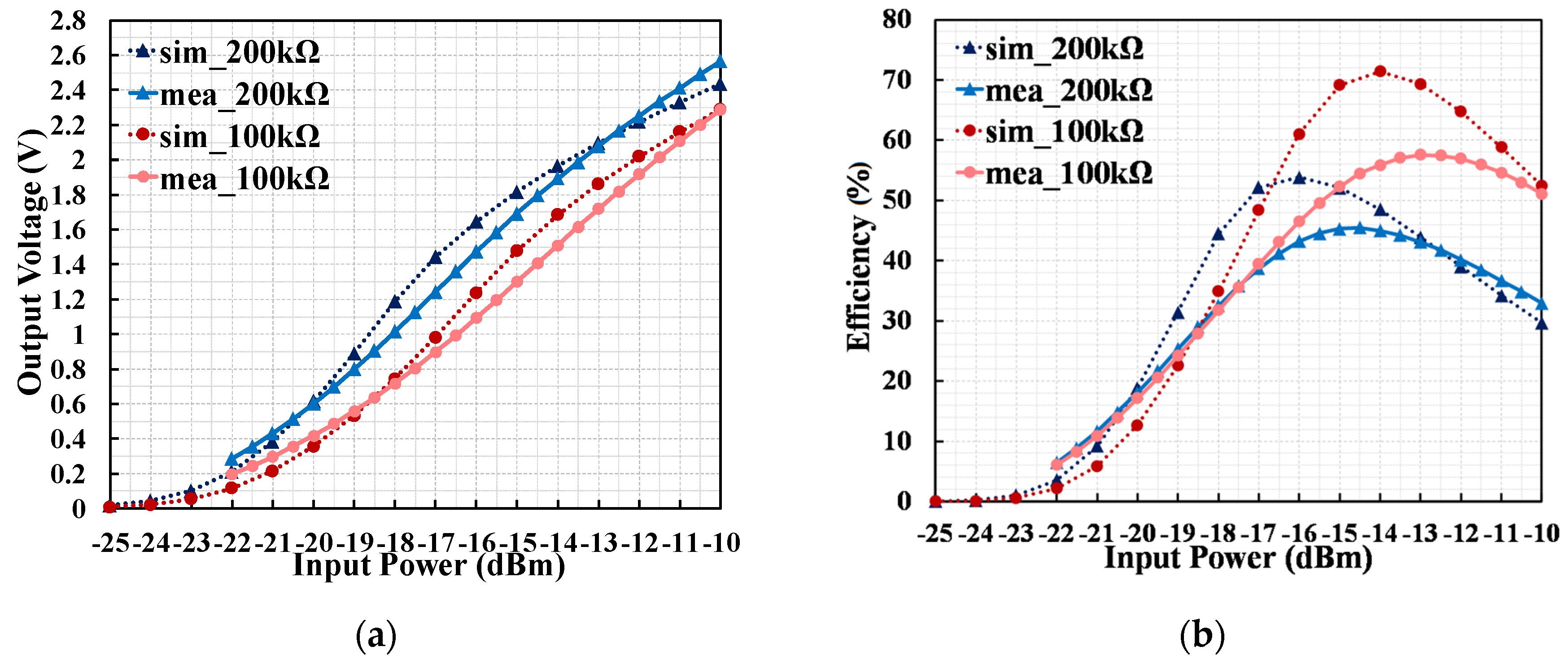
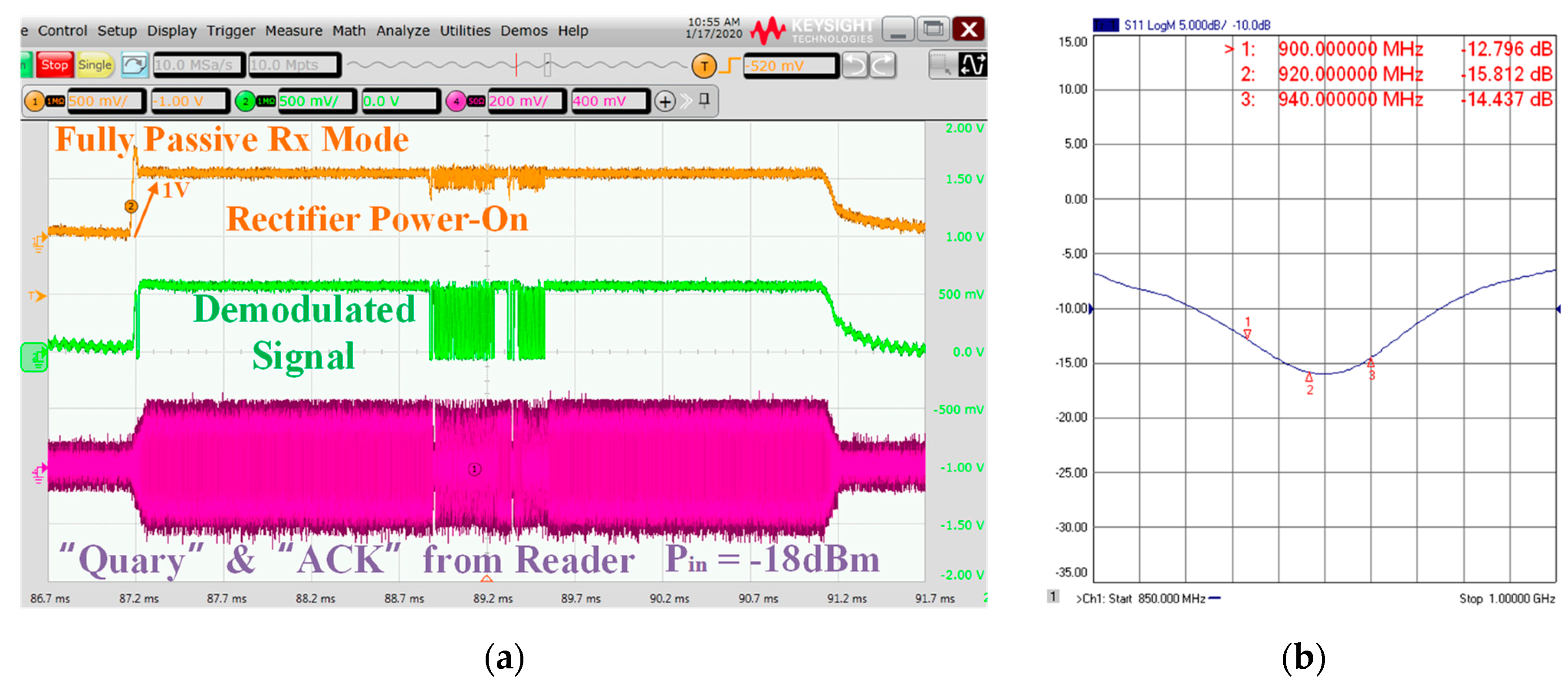
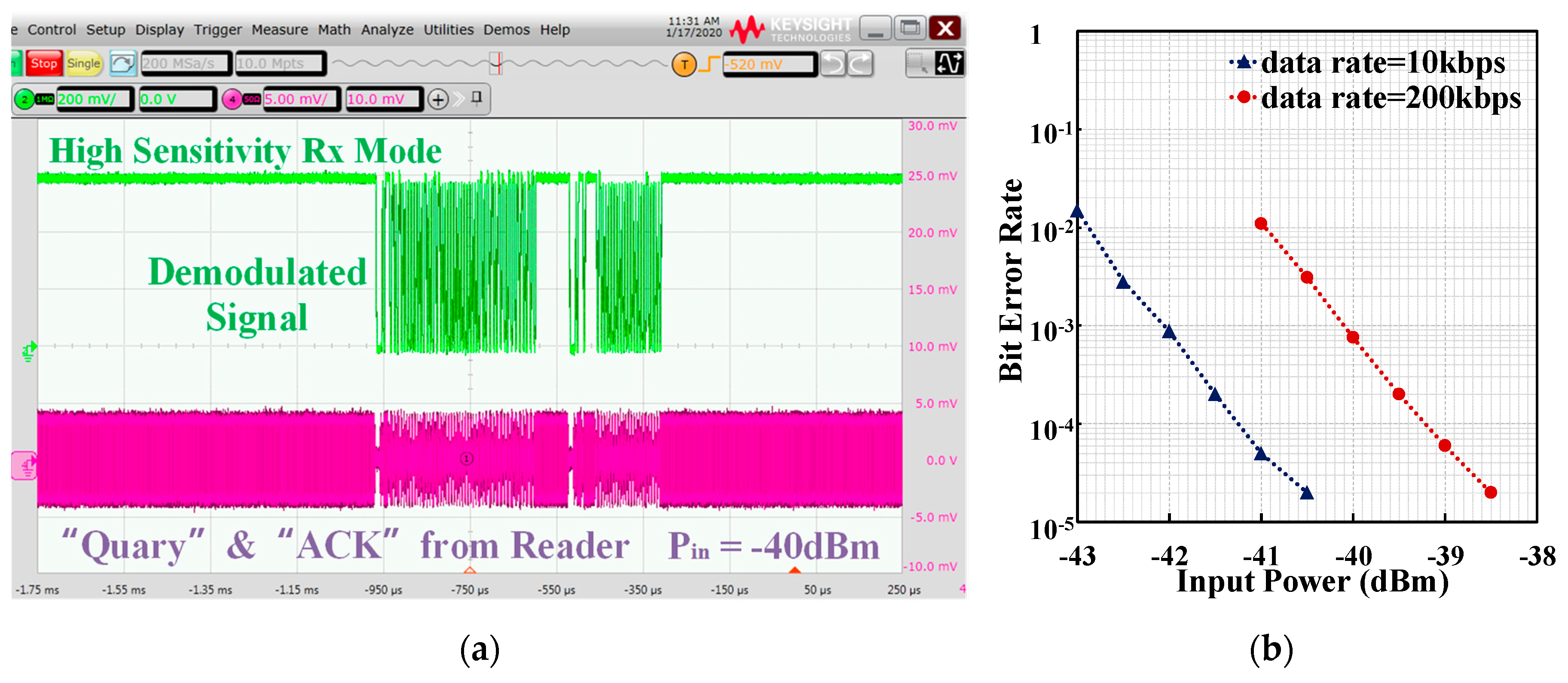
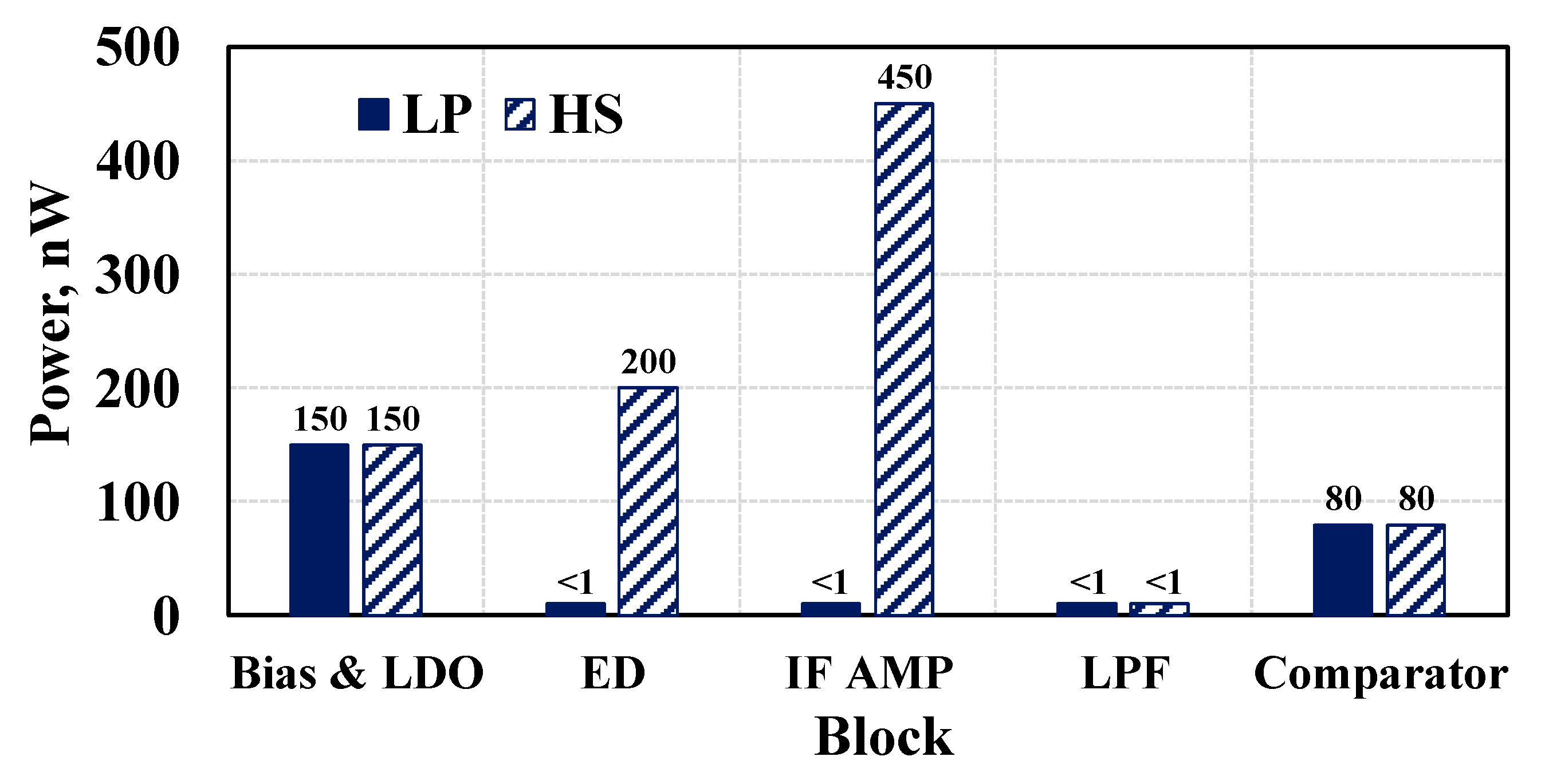
5. Measurement Results
6. Conclusions
Author Contributions
Funding
Acknowledgments
Conflicts of Interest
References
- Yin, J.; Yi, J.; Law, M.-K.; Ling, Y.; Lee, M.C.; Ng, K.P.; Gao, B.; Luong, H.C.; Bermak, A.; Chan, M.; et al. A System-on-Chip EPC Gen-2 Passive UHF RFID Tag With Embedded Temperature Sensor. IEEE J. Solid-State Circuits 2010, 45, 2404–2420. [Google Scholar]
- Che, W.; Meng, D.; Chang, X.; Chen, W.; Wang, L.; Yang, Y.; Xu, C.; Tan, X.; Yan, N.; Min, H. A Semi-Passive UHF RFID Tag with On-Chip Temperature Sensor. In Proceedings of the IEEE Custom Integrated Circuits Conference, San Jose, CA, USA, 19–22 September 2010; pp. 1–4. [Google Scholar]
- Neto, E.H.; Soares, R.; Conrad, E.; Costa, J.; Ramaswami, M. A Semi-Passive UHF RFID Tag Compliant with Brazilian National Automated Vehicle Identification System (SINIAV). In Proceedings of the IEEE International Conference on RFID-Technologies and Applications (RFID-TA), Nice, France, 5–7 November 2012; pp. 117–121. [Google Scholar]
- Yu, S.-M.; Feng, P.; Wu, N. Passive and Semi-Passive Wireless Temperature and Humidity Sensors Based on EPC Generation-2 UHF Protocol. IEEE Sens. J. 2014, 15, 2403–2411. [Google Scholar] [CrossRef] [Green Version]
- Jadhav, G.N.; Hamedi-Hagh, S. UHF Class-4 Active Two-Way RFID Tag for a Hybrid RFID-Based System. In Proceedings of the IEEE International RF & Microwave Conference, Seremban, Negeri Sembilan, Malaysia, 12–14 December 2011; pp. 337–342. [Google Scholar]
- Yang, T.; Xiang, J.; Wang, Y.; Tan, X.; Wang, J.; Yan, N.; Zheng, L.; Min, H. An Active Tag Using Carrier Recovery Circuit for EPC Gen2 Passive UHF RFID Systems. IEEE Trans. Ind. Electron. 2018, 65, 8925–8935. [Google Scholar] [CrossRef]
- Daly, D.C.; Chandrakasan, A.P. An Energy-Efficient OOK Transceiver for Wireless Sensor Networks. IEEE J. Solid-State Circuits 2007, 42, 1003–1011. [Google Scholar] [CrossRef] [Green Version]
- Yan, N.; Zhang, H.; Tan, X.; Min, H. Analysis and Design of a Multi-Mode Wake-Up Receiver Based on Direct Envelope Detection in Wireless Sensor Networks. IEEE Sens. J. 2018, 18, 9305–9314. [Google Scholar] [CrossRef]
- Moody, J.; Bassirian, P.; Roy, A.; Liu, N.; Pancrazio, S.; Barker, N.S.; Calhoun, B.H.; Bowers, S.M. A-76dBm 7.4nW wakeup radio with automatic offset compensation. In Proceedings of the IEEE International Solid—State Circuits Conference, San Francisco, CA, USA, 11–15 February 2018; pp. 452–454. [Google Scholar]
- Bandyopadhyay, S.; Chandrakasan, A.P. Platform Architecture for Solar, Thermal, and Vibration Energy Combining With MPPT and Single Inductor. IEEE J. Solid-State Circuits 2012, 47, 2199–2215. [Google Scholar] [CrossRef]
- Dondi, D.; Bertacchini, A.; Brunelli, D.; Larcher, L.; Benini, L. Modeling and Optimization of a Solar Energy Harvester System for Self-Powered Wireless Sensor Networks. IEEE Trans. Ind. Electron. 2008, 55, 2759–2766. [Google Scholar] [CrossRef]
- Wan, Q.; Teh, Y.K.; Gao, Y.; Mok, P.K.T. Analysis and Design of a Thermoelectric Energy Harvesting System With Reconfigurable Array of Thermoelectric Generators for IoT Applications. IEEE Trans. Circuits Syst. I: Regul. Pap. 2017, 64, 2346–2358. [Google Scholar] [CrossRef]
- Wan, Q.; Mok, P.K.T. A 14-nA, Highly Efficient Triple-Output Thermoelectric Energy Harvesting System Based on a Reconfigurable TEG Array. IEEE J. Solid-State Circuits 2019, 54, 1720–1732. [Google Scholar] [CrossRef]
- Yi, H.; Yin, J.; Mak, P.-I.; Martins, R.P. A 0.032-mm2 0.15-V Three-Stage Charge-Pump Scheme Using a Differential Bootstrapped Ring-VCO for Energy-Harvesting Applications. IEEE Trans. Circuits Syst. II: Express Briefs 2017, 65, 146–150. [Google Scholar] [CrossRef]
- Han, P.; Mei, N.; Zhang, Z. A UHF Semi-Passive RFID System with Photovoltaic/Thermoelectric Energy Harvesting for Wireless Sensor Networks. In Proceedings of the IEEE 13th International Conference on ASIC, Chongqing, China, 29 October–1 November 2019; pp. 1–4. [Google Scholar]
- Scorcioni, S.; Larcher, L.; Bertacchini, A. A Reconfigurable Differential CMOS RF Energy Scavenger With 60% Peak Efficiency and -21 dBm Sensitivity. IEEE Microw. Wirel. Compon. Lett. 2013, 23, 155–157. [Google Scholar] [CrossRef]
- Merenda, M.; Iero, D.; Della Corte, F.G. CMOS RF Transmitters with On-Chip Antenna for Passive RFID and IoT Nodes. Electronics 2019, 8, 1448. [Google Scholar] [CrossRef] [Green Version]
- Shi, Y.; Chen, X.; Kim, H.-S.; Blaauw, D.; Wentzloff, D. A 606μW mm-Scale Bluetooth Low-Energy Transmitter Using Co-Designed 3.5×3.5mm2 Loop Antenna and Transformer-Boost Power Oscillator. In Proceedings of the IEEE International Solid- State Circuits Conference, San Francisco, CA, USA, 17–21 February 2019; pp. 442–444. [Google Scholar]
- Han, P.; Zhang, Z.; Mei, N. Low-Power Passive/Active UHF RFID Tag Transceiver with Frequency Locked On-chip Oscillator. J. Circuits Syst. Comput. 2020. [Google Scholar] [CrossRef]
- Razavi, B. Design of Analog CMOS Integrated Circuits, 2nd ed.; McGraw Hill: New York, NY, USA, 2016; pp. 361–363. [Google Scholar]
- Gregorian, R. Introduction to CMOS OP-AMPs and Comparators; J Wiley & Sons: New York, NY, USA, 1999; pp. 195–197. [Google Scholar]


| Parameter | This Work | [6] TIE’ 18 | [8] Sensors J.’ 18 | [9] ISSCC’ 18 |
|---|---|---|---|---|
| Modulation | OOK | OOK | OOK | OOK |
| Carrier Frequency | 920 MHz | 920 MHz | 900 MHz | 433 MHz |
| Process | 180 nm CMOS | Discrete | 95 nm CMOS | 130 nm CMOS |
| Area | 0.455 mm2 | >100 mm2 | 0.18 mm2 | 1.95 mm2 |
| Energy Harvesting | RF/PV/TE | None | None | None |
| Receiver Architecture | Passive/Active ED + IF Amp | Envelope Detector | High-Q + Active ED + IF Amp | High-Q + Passive ED + Offset Control |
| Passive Voltage Gain | 8 dB | Not Reported | 25 dB | 27 dB |
| Sensitivity | −40 dBm @200 kbps | −39.5 dBm | −55 dBm @10 kbps | −71 dBm @200 bps |
| −42 dBm @10 kbps | ||||
| Power Consumption | 880 nW | >1 mW | 1 µW | 7.6 nW |
© 2020 by the authors. Licensee MDPI, Basel, Switzerland. This article is an open access article distributed under the terms and conditions of the Creative Commons Attribution (CC BY) license (http://creativecommons.org/licenses/by/4.0/).
Share and Cite
Han, P.; Zhang, Z.; Xia, Y.; Mei, N. A 920-MHz Dual-Mode Receiver with Energy Harvesting for UHF RFID Tag and IoT. Electronics 2020, 9, 1042. https://doi.org/10.3390/electronics9061042
Han P, Zhang Z, Xia Y, Mei N. A 920-MHz Dual-Mode Receiver with Energy Harvesting for UHF RFID Tag and IoT. Electronics. 2020; 9(6):1042. https://doi.org/10.3390/electronics9061042
Chicago/Turabian StyleHan, Peiqing, Zhaofeng Zhang, Yajun Xia, and Niansong Mei. 2020. "A 920-MHz Dual-Mode Receiver with Energy Harvesting for UHF RFID Tag and IoT" Electronics 9, no. 6: 1042. https://doi.org/10.3390/electronics9061042