Article

Disturbance Rejection and Control Design of MVDC Converter with Evaluation of Power Loss and Efficiency Comparison of SiC and Si Based Power Devices

by
Faisal Mehmood Shah
1,
Sarmad Maqsood
2,
Robertas Damaševičius
2,* and
Tomas Blažauskas
2
1
School of Electrical & Electronic Engineering, North China Electric Power University, Beijing 102206, China
2
Department of Software Engineering, Kaunas University of Technology, 51368 Kaunas, Lithuania
*
Author to whom correspondence should be addressed.
Electronics 2020, 9(11), 1878; https://doi.org/10.3390/electronics9111878
Submission received: 7 October 2020 / Revised: 4 November 2020 / Accepted: 5 November 2020 / Published: 8 November 2020
(This article belongs to the Section Power Electronics)

Abstract

:
With direct current (DC) power generation from renewable sources, as well as the current relocation of loads from alternating current (AC) to DC, medium-voltage DC (MVDC) should fill gaps in the areas of distribution and transmission, thereby improving energy efficiency. The MVDC system is a platform that interconnects electric power generation renewables (solar, wind) with loads such as data centers, industrial facilities and electric vehicle (EV) charging stations (also using MVDC technology). DC–DC power converters are part of the rising technology for interconnecting future DC grids, providing good controllability, reliability and bi-directional power flow. The contribution of this work is a novel and efficient multi-port DC–DC converter topology having interconnections between two converters, three-level neutral point clamping (NPC) on the high-voltage (HV) side and two converters on the low-voltage (LV) side, providing two nominal low voltages of 400 V (constant) and 500 V (variable), respectively. The design of this new and effective control strategy on the LV side has taken into condition load disturbances, fluctuations and voltage dips. A double-closed-loop control topology is suggested, where an outside voltage control loop (in which the capacitance energies are analyzed as variable, and the inside current loop is decoupled without the precise value of boost inductance) is used. The simulation results show the effectiveness of the proposed control system. In the second part of this study, wide-bandgap SiC and Si devices are compared by using comprehensive mathematical modeling and LT-spice software. Improving power loss efficiency and overall cost comparisons are also discussed.

1. Introduction

Direct current (DC) network systems are being analyzed and explored for use in future transmission and distribution technology due to advancements and maturity in the power electronic devices. Medium-voltage DC (MVDC) systems fill the gap in transmission and distribution areas, improving efficiency and energy delivery. In the future, MVDC grids would be the most flexible technique to collect renewable energy (e.g., solar, wind farms) and within industrial and urban area distribution networks. DC–DC high-power converters play a major role in the interconnection to MVDC grids, which must be capable to deal with unidirectional or bi-directional power flows. Compared to the medium-voltage alternating current (MVAC) system, the MVDC system shown in Figure 1 reduces cable weight, avoiding voltage dip problems at many points and easily parallels generators [1,2,3,4,5,6,7,8]. Moreover, most equipment in use employs DC; therefore, conversion stage losses will be reduced, and as a result the economy and efficiency could be improved [9]. However, MVDC acts as a foundation for developing a smart transportation system, which includes all electric trains, vehicles, planes and ships. Industrially, the first MVDC link between the UK and North Wales has recently been announced. The DC ANGLE project connects to the island of Anglesey by the Llanfair PG substation and to the North Wales mainland with Bangor operating at 27 kV DC along a 30.5 MW rating [10,11]. Due the recent development of new silicon carbide (SiC)-based semiconductor power devices, their use in markets is increasing due to their effectiveness and useful properties, such as significantly reducing conduction losses and switching losses in power converters, as well as improving converter efficiency. Thus, in many applications they would considered as an alternative to Si [12,13,14,15,16,17,18]. Currently, power semiconductor devices in the market (e.g., (SiC) silicon carbide MOSFET, Insulated Gate Bipolar Transistors (IGBTs)) are still expensive as compared to traditional Si (silicon). Consequently, this increases the cost of system, especially for higher-power converters that require a large number of power semiconductor devices. However, reducing the number of wide-bandgap (WBG) devices used in power converters will go a long way in the present industry in reducing costs [19].
In MVDC systems, the DC–DC converter is a key element, which acts as a transformer in current AC systems. The DC-based system performance depends on the DC converters because converters are responsible for changing voltage levels between the DC-based systems and delivering power. Therefore, the DC–DC converter has good reliability and performance, as needed for DC grids [10,20]. The DC–DC converter, which acts as the DC transformer, is one of the major key components in modern DC power grids and is connected to DC lines with variable voltage levels to make a DC network [21,22]. The MVDC DC–DC converter has drawn much attention in recent years; however, there are a number of major issues including protection and fault isolation, DC voltage regulation, output voltage control, voltage dip control, maintaining reliability and interconnecting different power lines [22,23,24,25,26]. All these DC–DC converters would have regulation capabilities, which provides balanced and stable voltage for back-end converters, improving system reliability and over-current control ability. In the MVDC power converters, Modular Multilevel Converter (MMC), flying capacitor, cascaded neutral point clamping (NPC) or active NPC (ANPC) topologies are usually used [27,28]. With an auto-transformer controlling two line-commutated current-sourced converters (LCCs), issues such as high-voltage DC (HVDC) interconnections, unreliability and power flow control are presented in [29]. Interactions between the boost converter and disturbance rejection have been shown [30]. Bi-directional DC–DC high-efficiency interconnections in MVDC and HVDC converters have been discussed in combination with two-level MMCs [31,32,33]. Modeling of MVDC multidrive systems for power quality analysis and harmonic injection is discussed in [34]. Robust voltage control and parametric uncertainties considering DC–DC converters are shown in [35]. A practical DC fault ride-through method for MMC-based MVDC distribution systems is proposed in [36]. For future distribution networks, a new, fast-acting backup protection strategy for embedded MVDC links is suggested in [37]. Modeling of the power SiC MOSFET module and predicting electromagnetic interference (EMI) of MVDC railway electrification system are shown in [38]. A wide-bandgap heterogeneous power device for high-frequency applications was discussed in [39]. Fault-tolerant operations for different modes of MVDC are suggested in [32,40]. In [41], a three-phase triple-active bridge converter interconnected with the MVDC grid along two nominal voltages is described. However, comparisons of disturbance rejection, uncertainty and power losses for MVDC-based converters are not addressed in these works.
In [14], the control variable is set as the square of the DC-bus voltage, and DC-bus voltage is set as the control variable compared to the conventional method. In the present topology, the outside voltage control loop (in which the capacitance energies are analyzed as variable) method is suggested because it can minimize stress to the capacitance voltage and reduce capacitance voltage deviations. The current topology is for industrial applications that work with step-down voltages of DC voltage 10 kV to 400 V and 500 V. The proposed study is composed of two parts. In the first part, the performance and control scheme is articulated for multiport DC–DC, an interconnections between the two converters are presented. A three-level neutral point clamping (NPC) is used on the high-voltage (HV) side, and a two-level phase is used on the low-voltage (LV) side along a rectifier circuit using two high-frequency transformers (HFT), including two nominal voltages as shown in the block diagram in Figure 2. The HV side provides a nominal voltage of 10 kV, while the LV side provides a nominal voltage of 400 V DC and 500 V DC, respectively (system overview is shown in Table 1). On the LV side, in designing the new and effective control strategy, the conditions of load disturbance voltage fluctuations and non-serious voltage dips are taken into consideration. In this study the double-closed-loop control topology is used inside the current loop and outside the voltage loop control; the outer voltage loop control comprises two parts: the inner current loop is decoupled without an exact boost inductance value, and the voltage control loop is proposed in which the capacitance energy is analyzed as a variable. Provided a constant 400 V and allowing 2.3% variation during parallel load changing (according to the IEEE standard, 5% variation is acceptable [42]), the simulation results have shown that the proposed control topology is effective. The focus of this study is mainly on the LV side.
In the second part of the paper, SiC and Si semiconductor power devices are compared, in which the conduction loss and switching loss, wide range of switching frequencies, cost comparisons and overall performance are evaluated. An accurate mathematical model was developed to represent the DC–DC converter in which efficiency is measured by using the equations presented in Appendix A under 75% and full-resistive load conditions. Simulations were carried out in LTSpice software. Although SiC power devices have multiple benefits in several applications, this article is focused on enhancing the efficiency of DC–DC bidirectional converters.
This study is organized as follows: in Section 2, the proposed control topology configuration on the LV side is presented. In Section 3, the simulation results of the proposed converter are discussed. In Section 4, the comparisons of power semiconductor devices and loss calculations in different load conditions are presented. Finally, in Section 5 the efficiency and cost comparisons are discussed in detail.

2. System Modeling and Control of DC–DC Three-Level MVDC Converter

Usually, in low-power and LV configurations, the two-level inverter topology is more attractive, but in high-power and HV drive applications, the three-level NPC topology is better because it generates very low harmonic distortion sinusoidal voltage waveforms by using the space vector pulse width modulation (SVPWM) switching technique. In this study, on the HV side the three-level NPC topology has been simulated using the SVPWM technique. The control scheme on the HV side inverter is shown in Figure 3 by using MATLAB/Simulink. In this research the main focus is only on the LV side.

3. Mathematical Model on the LV Side

Figure 4 [43] shows the power circuit of the three-phase voltage source rectifier topology. When designing this mathematical model we assumed a balanced three-phase system.
In the above figure, e a , e b and e c are the source voltages; i A , i B and i C are the line current; v a , v b and v c are the input rectifier voltage; v d c is DC output voltage; r is the resistance of the filter reactor; L is inductance of the filter reactor; R L is load resistance; i L is load current; V T 1 V T 2 are IGBTs; s j (j = 1–6) are switching functions,
The definition of switching function is
s j 1 , s j o p e n e d 0 , s j c l o s e d
The three-phase model of the voltage-sourced Pulse Width Modulated (PWM) rectifier can be expressed in the stationary a-b-c frame as (1), when the three-phase AC sources are balanced and the resistance of the power circuit is ignored.
L d i A d t + r i A = e a ( v a + U N O ) L d i B d t + r i B = e b ( v b + U N O ) L d i C d t + r i C = e c ( v c + U N O ) C d v d c d t + i A S a + i B S b + i C S c i L
The symmetry of the three-phase current and voltage is
v j = v d c s j , ( j = a , b , c ) U N O = U d c 3 ( s a , s b , s c )
Performing the park transformation, the mathematical model in the synchronous d q rotating frame can be expressed as
L d i d d t + r i d = e d v d + ω L i q L d i q d t + r i q = e q v q + ω L i d C d v d c d t = 1.5 ( i d s d + i q s q ) i L
where v d , v q and s d , s q are input voltages and switching function of the rectifier in synchronous rotating d q coordinates, respectively.

3.1. LV Side Control Design and Mathematical Model

At present, advanced modern control theory is growing rapidly, which has led to new ideas and thinking to solve complex problems. However, many of the control strategies are more difficult to implement in the industrial applications. Relatively, in various control systems the conventional proportional–integral (PI) controller is widely used due to its robustness and briefness. Based on internal modern theory, Figure 5 shows the diagram of the controller. For sufficient and essential conditions for zero-state error, the closed loop contains J R ( s ) as the input generation model. Therefore, the open loop transfer function is J R ( s ) = F ( s ) C ( s ) and also must have the input generation model.
Based on the internal model theory perspective, the zero steady-state error can be secured using the conventional PI controller, while the integration part contains s domain in the 1/s step signal. Therefore, to achieve the steady-state error the controller must contain a ω 2 /( s 2 + ω 2 ) part when the input signal is a sinusoidal r ( t ) , for example A s i n ( ω t), where the resonant controller is compulsory.

3.2. Design of Inner Current Loop

Figure 6 [44] shows the model of the three-phase voltage sourced rectifier d q frame.
Based on the synchronous d q rotating frame, the three-phase voltage-sourced rectifier and conventional control PI theory, the internal current loop is designed as follows:
v d r e f e d = K d P + K d i s ( i d r e f i d ) + ω L i q v q r e f e q = K q P + K d i s ( i d r e f i d ) + ω L i d
Figure 7 shows the obtained synchronous d q rotating frame and decoupling control diagram of the internal current loop. By using a conventional PI controller, the zero steady-state error can be secured because in the synchronous d q rotating frame the reference current is the constant DC signal.
where
c d ( s ) = K d i s + K d P c q ( s ) = K q i s + K q P
Therefore, to completely decouple the d q axis, the exact value of inductance L is essential. In some extreme conditions the value of inductance L will be changed; thus, part of the decoupling is often ignored. Hence, the enhanced coupling on the d q axis will lead to bad performance when the frequency increases.
With the model of the a-b-c three-phase rectifier, a two-phase α β reference frame model is obtained.
L d i α d t = e α v α r i α L d i β d t = e β v β r i β
Using the complex vector, the stationary reference frame model is shown in Equation (8).
L d i α β d t = e α β v α β r i α β
Thus, the model could be transformed into the rotating d q synchronous frame by replacing “d/dt” with “d/dt+j ω ” as shown in Equation (9).
d d t + j ω L i d q = e d q v d q r i d q
The model can also be shown as
d d t L i d q = e d q v d q ( r + j ω L ) i d q
Transforming into the s domain, the model can be shown as
I d q = ( E d q V d q ) 1 ( j ω L + r ) + s L = ( E d q V d q ) 1 L j ω + r L + s
Equation (11), therefore in the synchronous reference frame, shows the plant has only one complex pole found at - r / L - j ω . Hence, by choosing the proper parameters, the PI conventional controller would be zero, and approximately cancel the plant pole. In Equation (12) the controller is found as
C d q ( s ) = K p s j ω + K i K p + s = K p 1 s j ω + K i K p + 1
Based on the complex vector perspective, the rectifier model transforms the single-input single-output (SISO) model as of the double-input double-output (DIDO) model. Figure 8 shows the block diagram of the obtained decoupling control.
It can be observed in Figure 8, without an exact and accurate value of inductance, that good performance could be attained. The K i and K p parameters can be selected by following the conventional PI controller.
j ω + K i K p = j ω + r L
Hence, K i K p = r L by selecting proper value of K p , and a proper cutoff frequency can be chosen, as mentioned in Table 1.

3.3. Design Outer Voltage Loop

In consonance with the power-balancing principle, avoiding the losses in the rectifier, we take
P a c = P d c
The active input power is
P a c = v s a i s a + v s b i s b + v s c i s c
The equation in the synchronous d q reference frame turns into
P a c = 1.5 ( v s d i s d + v s q i s q )
where v s k , i s k (k = d , q ) are reactive and active elements of the input current and voltage in the d q synchronous frame. The DC side power can be described as
P d c = v d c i d c = v d c C d v d c d t + v d c 2 R L
Equation (16) is equal to Equation (17), then
v d c C d v d c d t + v d c 2 R L = 1.5 ( v s d i s d + v s q i s q )
From Equation (18), it can be seen that there are nonlinear items (i.e., the output voltage is squared, and it becomes a differential when multiplying the output voltage), which shows nonlinear relations among v d c and i s q , i s d .
The d-axis is commonly put in the same direction as the voltage vector in the synchronous d q reference frame. If the maximum value of three-phase voltage is v m , its symmetrical phase will be
v s d = V m v s q = 0
where v s q = 0. Thus, the v d c output voltage is calculated with only the variable i s d , and there is nonlinear relation among them.
In this study, the outer voltage control loop, a control scheme in which the capacitor energy is treated as a variable, is discussed. As there is a linear relation between the active current and capacitor energy, the system has great control characteristics with a simple PI controller. First, we analyze and transform the rectifier voltage, as shown in Equation (18).
d v d c 2 d t = 2 v d c d v d c d t
The equation will be
d v d c 2 d t = 2 R L C v d c 2 + 3 c v s d i s d + 3 c v s q i s q
where
w c = 1 2 C v d 2 c
v d c 2 = 2 W c C
Equation (21) will be
d d t w c = 2 R L C w c + 1.5 V s d i s d + 1.5 V s q i s q
If Equation (19) is put into Equation (24), then we obtain
d d t w c = 1.5 V m i s d 2 R L C w c
Equations (22) and (23) define the capacitor output energy. If w c , the capacitor energy, is considered as a new control variable, a linear relation will exist between i s d and w c , which is presented in Equation (25). The transformer function between the active current and capacitor current can be defined as
W c ( s ) I s d ( s ) = 1.5 V m s + 2 R L C
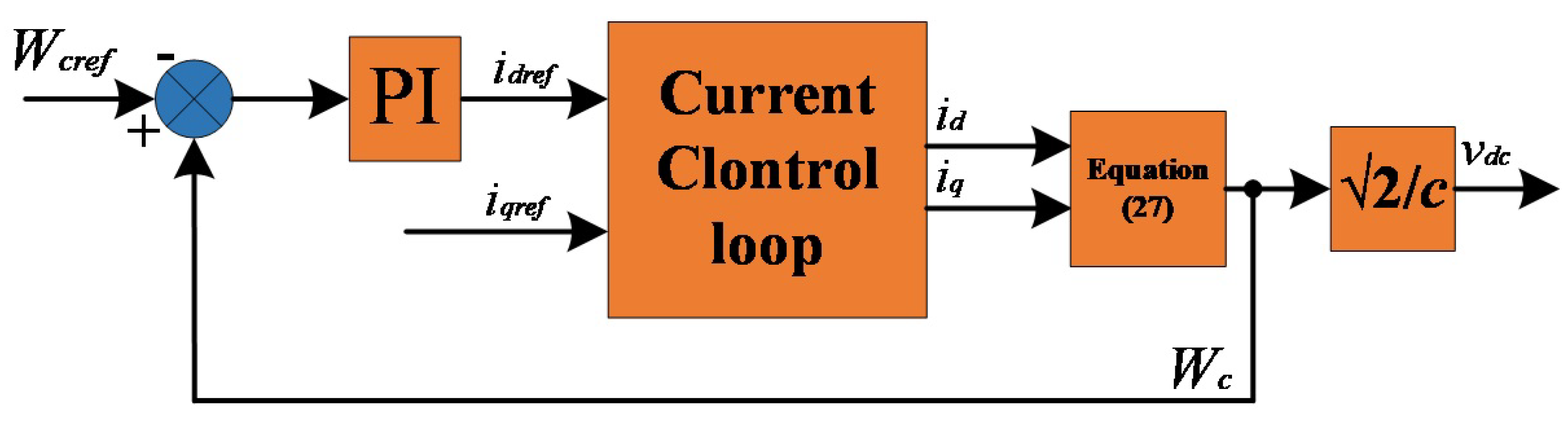
Capacitor energy is considered as a variable, and in the outer loop a linear PI regulator is used. If the capacitor energy is defined as W c r e f = 1/2 C V d c r e f 2 and the DC voltage reference is v d c r e f , the control system structure will be as shown in Figure 9.
The PI regulator transform function is described as
G P I ( s ) = K I v S + K p v
While selecting the controller in the double-closed-loop control system, it can be assured that the bandwidth of the internal current loop is wider than that of the outer voltage loop when examining the outer voltage control loop. In addition, the responding behavior of the current is quick enough to ignore the delay.
The closed-transform function system is defined as
W c ( s ) W c r e f ( s ) = 1.5 V m K P v S + K I v K P v s 2 + 2 R L C + 3 2 V m K I u s + 1.5 V m K I v
It is observable that the closed-loop transform function of capacitor energy is a second-order linear system. When S→0, the gain function will be W ( s ) / W r e f ( s ) →1, with a step response, which shows that the capacitor’s steady-state error and the steady-state error of the voltage are zero.

4. Simulation Results

To demonstrate the effectiveness and accuracy of the suggested control system for the DC–DC converter, simulations are carried out in MATLAB/Simulink software (MathWorks Inc, Natick, MA, USA), and parameters are specified in Table 1. First, on the HV side, the port (I) input DC voltage is a 20 kV waveform. Using the SVPWM technique, the line voltage modulation index is 0.8. After passing through the passive LC filter by reducing harmonics, the sinusoidal AC output of the 10 kV waveform is as shown in Figure 10. On the LV side, the port (III) input AC is 10 kV, and the line voltage, phase voltage and output constant 400 V are as shown in Figure 11. 
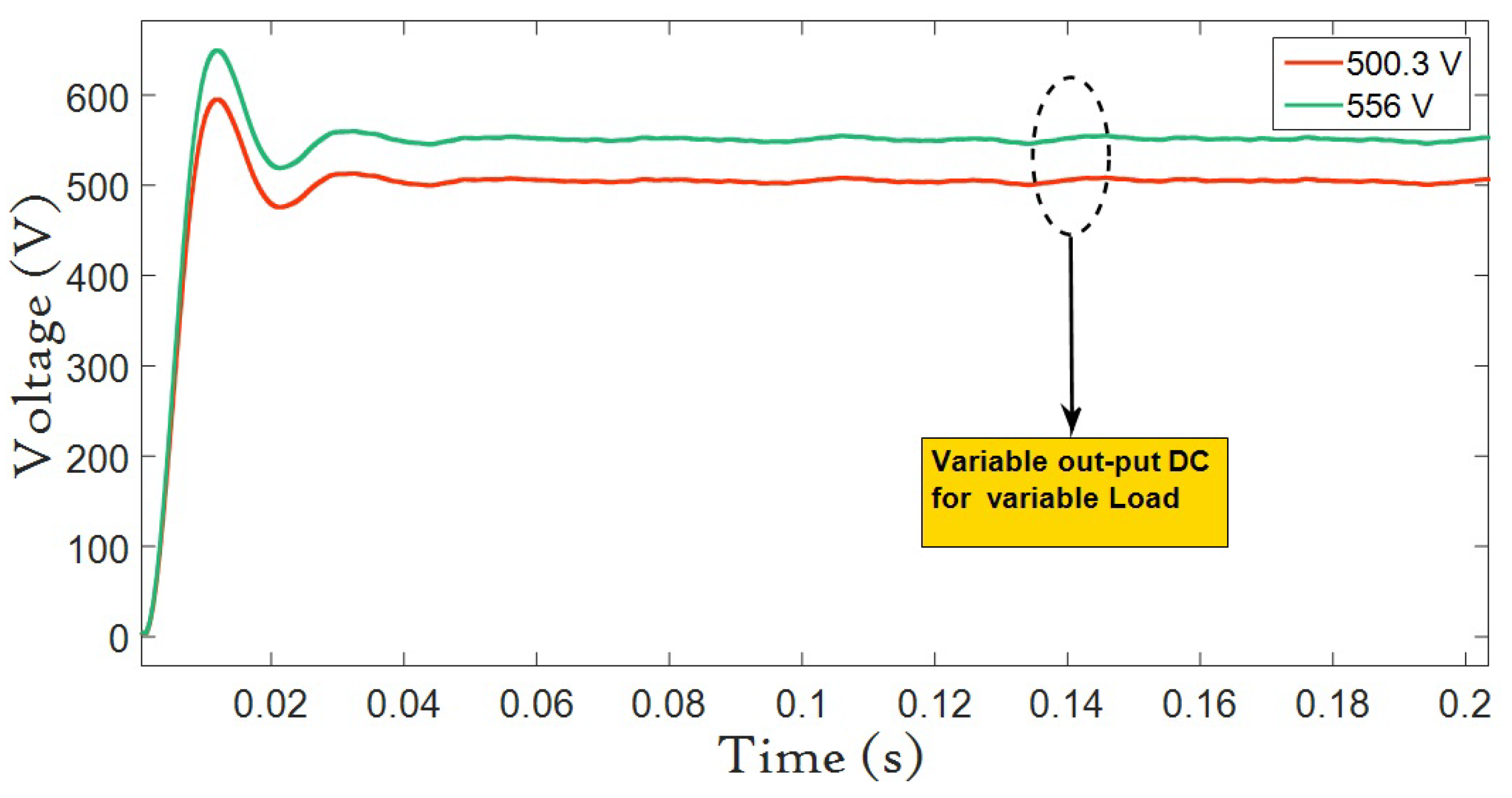
Figure 12 shows the different effects of loads when the load changes in parallel, and only 2.3% load variations will be accepted (according to IEEE standard, 5% variation is acceptable [44]). The output from port (II) 500 V variable output is shown in Figure 13, which changes according to load variation. Three-phase voltage and PQ are shown in Figure 14. The DC voltage waveform results are compared with [45]. We notice that the load changed from 50 Ω to 100 Ω at 0.14 s and is shown in Figure 15. The DC voltage reduced, there was a slight voltage dip, and then it tracked back to its original condition. It can be examined that the proposed topology is effective in conditions of uncertain load disturbances. The robustness of the suggested control system is proved, and the bidirectional power flow waveform for the current and voltage are clearly seen Figure 16. In Figure 17, the capacitor energy is shown as a variable. The simulation results show that the overshoot of the output voltage is reduced more than 70 V, so the control system has a superior performance.

5. DC–DC Converter Comparison Analysis

5.1. Devices Comparison and Analysis

A comparison study of semiconductor devices is shown in Table 2. The ratings are chosen according to how close the performances of the converters are to each other during operation at 400 V, 20 A and 150 ° C, and key parameters are obtained from their respective datasheets.
Because of the higher breakdown voltage, low state resistance, much lower parasitic capacitance and higher switching frequency compared to Si, SiC technology minimizes losses and volume. In this section the semiconductor devices are compared, and conduction loss and switching loss, efficiency, wide range of switching frequencies, costs and overall performances are evaluated. The process life cycle is shown in Figure 18. An accurate mathematical model was developed to represent the DC–DC converter’s overall performance, and loss was calculated using the equations in Appendix A under 75% and full-resistive load conditions. Datasheet extrapolations were used, and simulations were carried out in LTSpice software (Analog Devices, Norwood, Massachusetts, USA), where the SiC MOSFET model was created according to datasheet and manufacturer specifications.

5.2. Converter Performance at Variable Switching Frequencies

The total power loss ( P L ) of the converter is acquired by the sum of switching losses ( P s w ), conduction losses ( P c o n d u c t i o n ) and the capacitor inductor loss ( P i c ). It can be obtained by the following equation:
P L = P s w + P c o n d u c t i o n + P i c
Specifications of the DC–DC converter are presented in Table 3. The conduction and switching losses were calculated for V d c = 400 V, P o u t = 15 kW and R g a t e = 10 Ω .
Conduction losses for every switching cycle were calculated, and loss created by the transistor junction temperature, on-resistance and transistor current were evaluated. The switching losses were determined based on turn-off and turn-on energy, transistor voltage, gate resistor, transistor current and junction temperature. According to the SiC MOSFET and Si IGBT transistor datasheets, reverse recovery energy is included during turn-off and turn-on phases. Hence, it is not compulsory to consider these losses independently. Energy stored in the output capacitance of the transistor was also included in the turn-off and turn-on energy states.
The total power losses are shown in Figure 19 and Figure 20 at three junction temperatures of 25 ° C, 100 ° C and 150 ° C when the switching frequency was increased from 10 to 100 kHz. The results reveal that SiC had lower losses in the considered switching frequency range at low junction temperatures. At high junction temperature, it is clearly seen in the diagrams that the total SiC losses were below total Si losses; hence, it is noteworthy that the influence of increased junction temperature on the total power losses in the SiC MOSFET-based converter was lower than that of Si IGBT due to the higher thermal conductivity of SiC materials.

5.3. Simulation and Analysis

Some specifications of the DC–DC converter are shown in Table 4. The specifications are chosen according to converter model.
Simulations were carried out in LTSpice software. The SiC MOSFET model from CREE (Research Triangle Park, North Carolina, United States) was created according to datasheet and manufacturer specifications. A mathematical model was developed to represent the converter’s overall performance and loss calculations and by using the equations in Appendix A under 75% and full-resistive load conditions. The calculation results are shown in Figure 21 and Table 5.
As it can be seen in Figure 21, the output voltage of the DC–DC converter was 397 V, with peak-to-peak ripple less than that 5 V. The average inductor current was 60 A, with 3 A peak-to-peak ripple current, which meets the low ripple current requirement. Since SiC MOSFET has small input capacitance, the gate driver is able to fully turn off and turn on the device faster than the Si MOSFET, as shown in Figure 22.
The above mathematical results show that by using SiC devices, both switching and conduction losses decreased, which is expected according our prediction. It is notable that SiC MOSFET had a total switching loss ( P s w ) of only 33 W at full and 30 W at 75% load, respectively, which is almost one-fifth of the total switching losses of Si IGBT. The conduction loss ( P c o n d u c t i o n ) of SiC MOSFET was also reduced 40–45% as compared to the Si design and capacitor and inductor losses ( P i c ) are nearly the same because the component ESRs and root mean square (RMS) current values are same). The overall efficiency of the SiC design was 99.06% at full load and 98.82 for 75% load; it is 1.85% higher than that for all Si design models. From Figure 23 it is clearly seen that all three SiC portions (switching loss, conduction loss and capacitor loss) were superior; hence, for higher-frequency operations the SiC converter has a better potential for use than the Si.
In Figure 24, at 75% load the efficiency of the converter was slightly better than at full load; this is due to the current squared relationship, and the resistive loss components will drop down to 1/4 of the original value, while the resistance value will not change. In Table 5, capacitor and inductor loss ( P i c ) exactly followed this rule, but conduction loss ( P c o n d u c t i o n ) did not. In the Si IGBT case, conduction losses were not purely resistive, but in the MOSFET case, conduction losses were resistive. Thus, conduction loss in the SiC MOSFET case were smaller compared to Si as the load decreased. Furthermore, the switching losses were also reduced as compared to full load. Other losses (gate driver power consumption) were not included, as efficiency would be affected if these losses were included.

6. Cost Comparison

In order to compare SiC and Si costs, running and initial prices were taken into account. The initial prices of SiC MOSFET (C2M0080120D) and Si IGBT (NGTB20N120LWG) devices, which are used in the converters, have been summarized in Table 6. All prices were taken from the Farnell (Leeds, UK) website on 29 Jan 2020, at 100 pieces. The heat sinks were also found on the Farnell website and chosen on the basis of temperature increases for the given power loss.
The costs of semiconductors are compared in Figure 25. It can be seen in Table 6 that the cost of SiC MOSFET was more than double that of Si IGBT because of the drivers cost. The drivers of SiC are expensive because a special driving scheme is needed to support the SiC. On the other hand, the cooling requirements for Si are much greater than for SiC; thus, the cost difference is not as big a barrier as one may have expected.

7. Conclusions

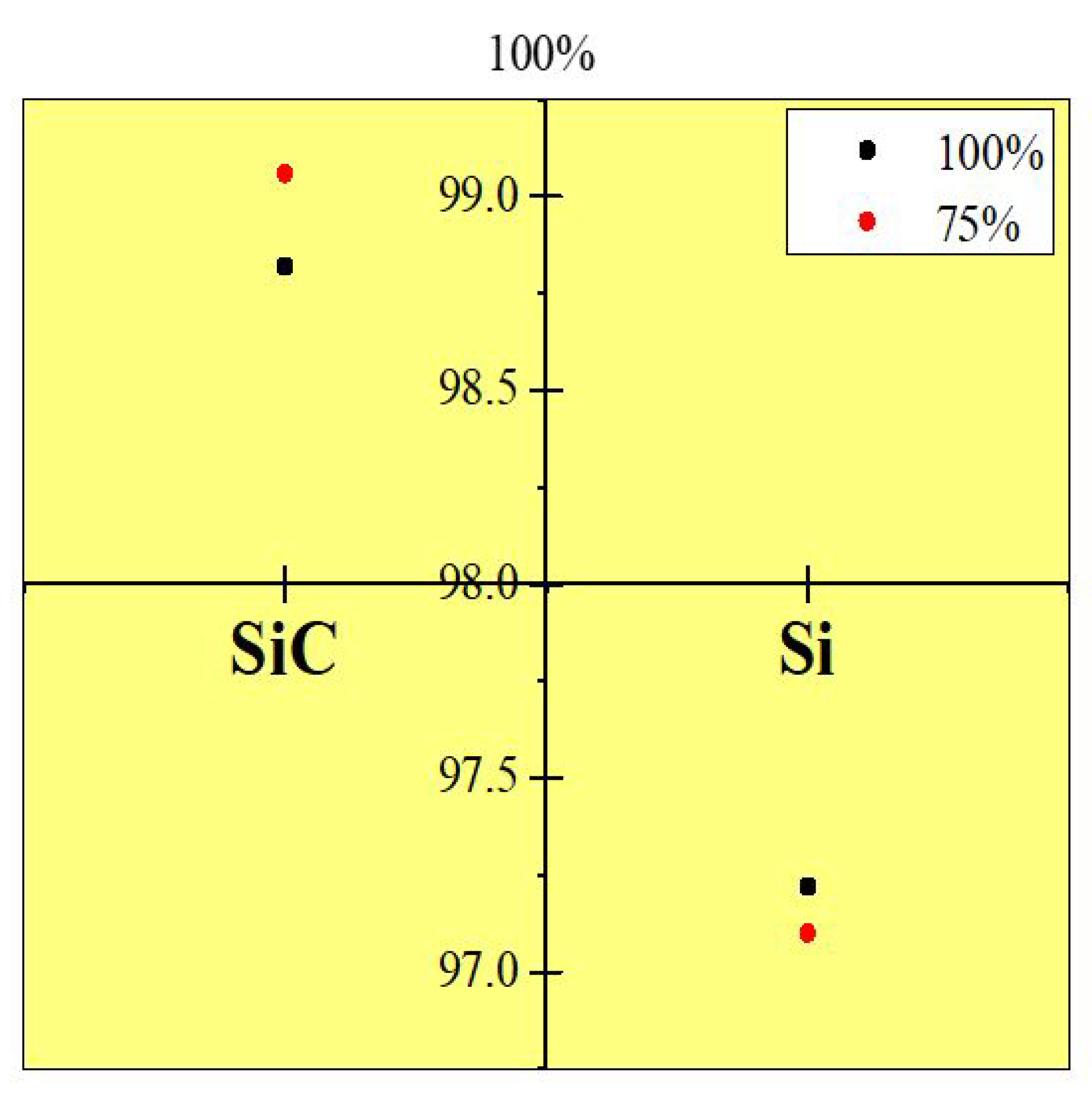
A comprehensive performance study of a proposed MVDC DC–DC three-level converter has been presented. The suggested multi-port converter on the LV side provides two nominal voltages of 400 V (constant) and 500 V (variable), respectively. A novel and effective double-closed-loop control strategy on the LV side was analyzed in two scenarios. In a voltage control scheme, according to the investigation, the capacitor energy is analyzed as a variable, and the dynamic response of the output voltage is improved. An inner current loop control was also analyzed without an exact inductance value in complex vector frame. When designing the controllers, uncertain load disturbances during voltage dips were taken into account. The simulation results demonstrate that the fluctuations and voltage dips can be controlled effectively by applying the proposed control topology. Consequently, this topology is effective and applicable to enhance the robustness and energy conversation of a system. In the second portion, a comparison study between new SiC and Si semiconductor power devices is given. Test simulations for both devices were built and verified. The performance and operation of semiconductors were compared at different specifications, and conduction loss switching loss, wide range of switching frequencies, cost comparisons and overall performances were evaluated. The efficiency of the SiC-based converter was found above 99% under two resistive load conditions, which shows the efficiency of the SiC-based converter is 1.85% higher than that of Si. SiC MOSFET can also operate at higher temperatures, and less cooling is required because of the decrease in device losses. Costs of both devices were compared. SiC drivers are expensive, but the cooling requirement for Si is much greater than that of SiC; thus, the cost difference is not a big barrier. The outcomes of this study are valid for all kinds of DC–DC converters used in numerous other applications. Therefore, this study is helpful to enhance the reliability, and improve the overall efficiency, of converters that can be derived in the future.

Author Contributions

Conceptualization: F.M.S., and S.M.; methodology: F.M.S., and S.M.; software: F.M.S., and S.M.; validation: F.M.S., S.M., and R.D.; formal analysis: F.M.S., S.M., and R.D.; investigation: F.M.S., S.M., R.D. and T.B.; data curation: F.M.S., and S.M.; writing—original draft preparation: F.M.S., and S.M.; supervision: R.D.; project administration: R.D. and T.B.; funding acquisition: R.D. and T.B. All authors have read and agreed to the published version of the manuscript.

Funding

This research received no external funding.

Conflicts of Interest

The authors declare no conflict of interest.

Appendix A

Table 1: Devices loss calculation model.
Conduction losses—two-level converter
P c T 1 , T 2 = V o , T I L ^ 2 π 1 + M π 4 c o s ( φ ) + r 0 , T I L 2 ^ 2 π π 4 + 2 M 3 c o s ( φ )
P c D 1 , D 2 = V o , D I L ^ 2 π 1 M π 4 c o s ( φ ) + r 0 , D I L 2 ^ 2 π π 4 2 M 3 c o s ( φ )
Switching losses—two-level converter
P s T 1 , T 2 = f s π ( E o n + E o f f ) V d c V r e f I L ^ I r e f
P s D 1 , D 2 = f s π E r r V d c V r e f I L ^ I r e f
Conduction losses—three-level NPC
P c T 1 , T 4 = V o , T M I L ^ 4 π [ s i n ( φ ) + ( π φ ) c o s ( φ ) ] + r o , T M I L 2 ^ 4 π 8 3 c o s 4 φ 2
P c D 1 , D 4 = V o , D M I L ^ 4 π [ s i n ( φ ) φ c o s ( φ ) ] + r o , D M I L 2 ^ 2 4 3 π s i n 4 φ 2
P c T 2 , T 3 = V o , D I L ^ π 1 M 4 ( s i n ( φ ) φ c o s ( φ ) ) + r o , T I L 2 ^ 4 1 8 M 3 π s i n 4 φ 2
P c D 2 , D 3 = V o , D M I L ^ 4 π [ s i n ( φ ) φ c o s ( φ ) ] + r o , D M I L 2 ^ 2 4 3 π s i n 4 φ 2
P c D 5 , D 6 = V o , D I L ^ π 1 M 4 ( 2 s i n ( φ ) ( 2 φ π ) c o s ( φ ) ) + r o , D I L 2 ^ 4 1 4 M 3 π ( 1 + c o s 2 ( φ ) )
Switching losses—three-level NPC
P s T 1 , T 4 = f s ( E o n + E o f f ) 0.5 V d c V r e f I L ^ I r e f 1 + c o s ( φ ) 2 π
P s D 1 , D 4 = f s E r r 0.5 V d c V r e f I L ^ I r e f 1 c o s ( φ ) 2 π
P s T 2 , T 3 = f s ( E o n + E o f f ) 0.5 V d c V r e f I L ^ I r e f 1 c o s ( φ ) 2 π
P s D 2 , D 3 = 0
P s D 5 , D 6 = f E r r 0.5 V d c V r e f I ^ I r e f 1 + c o s ( φ ) 2 π

References

  1. Mesas, J.J.; Monjo, L.; Sainz, L.; Pedra, J. Study of MVDC system benchmark networks. In Proceedings of the International Symposium on Smart Electric Distribution Systems and Technologies (EDST), Vienna, Austria, 8–11 September 2015. [Google Scholar]
  2. Liu, C.; Kong, D.; Zhang, Z.; Pei, Z.; Kennel, R. Single-Stage Control System of I-MMC-Based Island MVDC Link Receiver with Multiple Modulation Freedoms. IEEE Access 2020, 8, 10088–10097. [Google Scholar] [CrossRef]
  3. Stieneker, M.; Doncker, R.W.D. Medium-voltage DC distribution grids in urban areas. In Proceedings of the IEEE 7th International Symposium on Power Electronics for Distributed Generation Systems (PEDG), Vancouver, BC, Canada, 27–30 June 2016. [Google Scholar]
  4. Lee, Y.; Vakil, G.; Watson, A.J.; Wheeler, P.W. An analytical modeling and estimating losses of power semiconductors in a three-phase dual active bridge converter for MVDC grids. In Proceedings of the IEEE Power and Energy Conference at Illinois (PECI), Vancouver, BC, Canada, 27–30 June 2017. [Google Scholar]
  5. Chen, Y.; Li, Z.; Zhao, S.; Wei, X.; Kang, Y. Design and Implementation of a Modular Multilevel Converter with Hierarchical Redundancy Ability for Electric Ship MVDC System. IEEE J. Emerg. Sel. Top. Power Electron. 2017, 5, 189–202. [Google Scholar] [CrossRef]
  6. Ayodelea, E.; Misrab, S.; Damasevicius, R.; Maskeliunas, R. Hybrid microgrid for microfinance institutions in rural areas—A field demonstration in West Africa. Sustain. Energy Technol. Assessments 2019, 35, 89–97. [Google Scholar] [CrossRef]
  7. Jain, V.; Chaudhary, G.; Taplamacioglu, M.C.; Agarwal, M.S. Advances in Data Sciences, Security and Applications. In Proceedings of ICDSSA 2019; Springer: Berlin/Heidelberg, Germany, 2019. [Google Scholar]
  8. Ogunleye, O.; Alabi, A.; Misra, S.; Adewumi, A.; Ahuja, R.; Damasevicius, R. Comparative Study of the Electrical Energy Consumption and Cost for a Residential Building on Fully AC Loads Vis-a-Vis One on Fully DC Loads. In Lecture Notes in Electrical Engineering; Springer: Singapore, 2019; pp. 395–405. [Google Scholar]
  9. Ma, J.; Geng, G.; Jiang, Q. Two-Time-Scale Coordinated Energy Management for Medium-Voltage DC Systems. IEEE Trans. Power Syst. 2016, 31, 3971–3983. [Google Scholar] [CrossRef]
  10. Aboushady, A.A.; Ahmed, K.H.; Finney, S.J.; Williams, B.W. Lyapunov-based high-performance controller for modular resonant DC/DC converters for medium-voltage DC grids. IET Power Electron. 2017, 10, 2055–2064. [Google Scholar] [CrossRef] [Green Version]
  11. Yu, J.; Smith, K.; Urizarbarrena, M.; MacLeod, N.; Bryans, R.; Moon, A. Initial designs for the ANGLE DC project; converting existing AC cable and overhead line into DC operation. In Proceedings of the 13th IET International Conference on AC and DC Power Transmission (ACDC 2017), Manchester, UK, 14–16 February 2017. [Google Scholar]
  12. Cardenas, R.B.; Isobe, T.; Molinas, M. Comparative study of semiconductor devices based on a meta-parameterised approach: SiC MOSFET vs Si IGBT technologies. In Proceedings of the IEEE 8th International Power Electronics and Motion Control Conference (IPEMC-ECCE Asia), Hefei, China, 22–26 May 2016. [Google Scholar]
  13. Anthon, A.; Zhang, Z.; Andersen, M.A.E.; Holmes, D.G.; McGrath, B.; Teixeira, C.A. Comparative Evaluation of the Loss and Thermal Performance of Advanced Three-Level Inverter Topologies. IEEE Trans. Ind. Appl. 2017, 53, 1381–1389. [Google Scholar] [CrossRef] [Green Version]
  14. Shah, F.M.; Maqsood, S.; Shah, Z.M.; Muhammad, F.; Kim, S. Multilevel LVDC Distribution System with Voltage Unbalancing and Disturbance Rejection Control Topology. IEEE Access 2020, 8, 133787–133801. [Google Scholar] [CrossRef]
  15. Slawinski, M.; Heer, D.; Villbusch, T.; Buschkuehle, M. System study of SiC MOSFET and Si IGBT power module performance using a bidirectional buck-boost converter as evaluation platform. In Proceedings of the 18th European Conference on Power Electronics and Applications (EPE’16 ECCE Europe), Karlsruhe, Germany, 5–9 September 2016. [Google Scholar]
  16. Shah, F.M.; Xiao, H.M.; Li, R.; Awais, M.; Zhou, G.; Bitew, G.T. Comparative performance evaluation of temperature dependent characteristics and power converter using GaN, SiC and Si power devices. In Proceedings of the IEEE 12th International Conference on Compatibility, Power Electronics and Power Engineering (CPE-POWERENG 2018), Doha, Qatar, 10–12 April 2018; pp. 1–7. [Google Scholar]
  17. Shah, F.M.; Minxiao, H.; Muhammad, T.; Xxie, W.; Awais, M. Three-Phase AC-DC Voltage Disturbance Rejection Control Strategy by Using Inverter Decoupling Topology. In Proceedings of the International Conference on Power Generation Systems and Renewable Energy Technologies (PGSRET), Islamabad, Pakistan, 10–12 September 2018; pp. 1–5. [Google Scholar]
  18. Kiani, S.H.; Altaf, A.; Abdullah, M.; Muhammad, F.; Shoaib, N.; Anjum, M.R.; Damaševičius, R.; Blažauskas, T. Eight Element Side Edged Framed MIMO Antenna Array for Future 5G Smart Phones. Micromachines 2020, 11, 956. [Google Scholar] [CrossRef]
  19. He, J.; Katebi, R.; Weise, N. A Current-Dependent Switching Strategy for Si/SiC Hybrid Switch-Based Power Converters. IEEE Trans. Ind. Electron. 2017, 64, 8344–8352. [Google Scholar] [CrossRef] [Green Version]
  20. Liu, D.; Deng, F.; Chen, Z. Five-Level Active-Neutral-Point-Clamped DC/DC Converter for Medium-Voltage DC Grids. IEEE Trans. Power Electron. 2017, 32, 3402–3412. [Google Scholar] [CrossRef]
  21. Wang, X.; Tang, G.; He, Z.; Wei, X.; Pang, H.; Xiao, X. Modeling and control of an isolated module multilevel DC/DC converter for DC grid. CSEE J. Power Energy Syst. 2017, 3, 150–159. [Google Scholar] [CrossRef]
  22. Xie, R.; Li, H. Fault Performance Comparison Study of a Dual Active Bridge (DAB) Converter and an Isolated Modular Multilevel DC/DC (iM2DC) Converter for Power Conversion Module Application in a Breaker-Less Shipboard MVDC System. IEEE Trans. Ind. Appl. 2018, 54, 5444–5455. [Google Scholar] [CrossRef]
  23. Harrye, Y.A.; Aboushady, A.A.; Ahmed, K.H. Power sharing controller for modular dual active bridge DC/DC converter in medium voltage DC applications. In Proceedings of the IEEE 6th International Conference on Renewable Energy Research and Applications (ICRERA), San Diego, CA, USA, 5–8 November 2017. [Google Scholar]
  24. Jovcic, D.; Zhang, H. Dual Channel Control with DC Fault Ride Through for MMC-Based, Isolated DC/DC Converter. IEEE Trans. Power Deliv. 2017, 32, 1574–1582. [Google Scholar] [CrossRef]
  25. Farhadi, M.; Abapour, M.; Sabahi, M. Failure analysis and reliability evaluation of modulation techniques for neutral point clamped inverters-A usage model approach. Eng. Fail. Anal. 2017, 71, 90–104. [Google Scholar] [CrossRef] [Green Version]
  26. Han, Q.; Li, B.; Li, Z.; Ke, Q. Research of grid-connected photovoltaic inverter grid-connected system based on dual closed-loop of grid voltage vector orientation. In Proceedings of the Chinese Automation Congress (CAC), Jinan, China, 20–22 October 2017. [Google Scholar]
  27. Chen, Y.; Zhao, S.; Li, Z.; Wei, X.; Kang, Y. Modeling and Control of the Isolated DC-DC Modular Multilevel Converter for Electric Ship Medium Voltage Direct Current Power System. IEEE J. Emerg. Sel. Top. Power Electron. 2017, 5, 124–139. [Google Scholar] [CrossRef]
  28. Jafarishiadeh, S.; Farasat, M.; Sadigh, A.K. Medium-voltage DC grid connection using modular multilevel converter. In Proceedings of the IEEE Energy Conversion Congress and Exposition (ECCE), Cincinnati, OH, USA, 1–5 October 2017. [Google Scholar]
  29. Lu, S.; Lin, W.; Yao, W.; Wen, J. Control of two LCC-HVDC interconnected through DC-DC autotransformer. In Proceedings of the 12th IET International Conference on AC and DC Power Transmission (ACDC 2016), Beijing, China, 28–29 May 2016. [Google Scholar]
  30. Mendez, A.H.; Flores, J.L.; Ramirez, H.S.; Castellanos, J.F.G.; Aguilar, G.M. A Backstepping Approach to Decentralized Active Disturbance Rejection Control of Interacting Boost Converters. IEEE Trans. Ind. Appl. 2017, 53, 4063–4072. [Google Scholar] [CrossRef]
  31. Cui, S.; Soltau, N.; Doncker, R.W.D. A High Step-Up Ratio Soft-Switching DC-DC Converter for Interconnection of MVDC and HVDC Grids. IEEE Trans. Power Electron. 2018, 33, 2986–3001. [Google Scholar] [CrossRef]
  32. Cui, S.; Hu, J.; Doncker, R.D. Fault-Tolerant Operation of a TLC-MMC Hybrid DC-DC Converter for Interconnection of MVDC and HVdc Grids. IEEE Trans. Power Electron. 2020, 35, 83–93. [Google Scholar] [CrossRef]
  33. Du, S.; Wu, B.; Zargari, N.R. A Transformerless High-Voltage DC-DC Converter for DC Grid Interconnection. IEEE Trans. Power Deliv. 2018, 53, 282–290. [Google Scholar] [CrossRef]
  34. Ruiz, A.S.; Valera, J.J.; Legarra, I.; Torre, I.; Telleria, S.; Atutxa, I. Modelling of MVDC Multidrive Systems for Power Quality Analysis. IEEE Trans. Ind. Electron. 2020. [Google Scholar]
  35. Rocha, E.M.; Barra, W.; Lucas, K.E.; Medeiros, R.L.P.; Vaca-Benavides, D.A. Design and Experimental Assessment of a Robust Voltage Control for DC-DC Converters Considering Components Parametric Uncertainties. IEEE Access 2020, 8, 109217–109231. [Google Scholar] [CrossRef]
  36. Wang, Y.; Li, Q.; Li, B.; Wei, T.; Zhu, Z.; Li, W.; Wen, W.; Wang, C. A Practical DC Fault Ride-Through Method for MMC based MVDC Distribution Systems. IEEE Trans. Power Deliv. 2020. [Google Scholar] [CrossRef]
  37. Hunter, L.; Booth, C.D.; Alvarez, A.E.; Dysko, A.; Finney, S.; Ferre, A.J. A new fast-acting backup protection strategy for embedded MVDC links in future distribution networks. IEEE Trans. Power Deliv. 2020. [Google Scholar] [CrossRef]
  38. Zhu, R.; Liang, T.; Dinavahi, V.; Liang, G. Wideband Modeling of Power SiC mosfet Module and Conducted EMI Prediction of MVDC Railway Electrification System. IEEE Trans. Electromagn. Compat. 2020. [Google Scholar] [CrossRef]
  39. Xu, J.; Gu, L.; Ye, Z.; Kargarrazi, S.; Rivas-Davila, J.M. Cascode GaN/SiC: A Wide-Bandgap Heterogenous Power Device for High-Frequency Applications. IEEE Trans. Power Electron. 2020, 35, 6340–6349. [Google Scholar] [CrossRef]
  40. Geng, Z.; Han, M. Fault Localization Strategy for Modular Multilevel Converters in Rectifier Mode under Submodule Switch Open-Circuit Failure. IEEE Trans. Circuits Syst. II Express Briefs 2020. [Google Scholar] [CrossRef]
  41. Neubert, M.; Gorodnichev, A.; Gottschlich, J.; Doncker, R.W.D. Performance analysis of a triple-active bridge converter for interconnection of future dc-grids. In Proceedings of the IEEE Energy Conversion Congress and Exposition (ECCE), Milwaukee, MI, USA, 18–22 September 2016. [Google Scholar]
  42. Barros, J.; Saiz, P.; de Apraiz, M.; Leturiondo, L.A.; Diego, R.I.; Gutierrez, J.J. Limitations in the use of the IEC standard method for detection and analysis of rapid voltage changes in power system networks. In Proceedings of the 17th International Conference on Harmonics and Quality of Power (ICHQP), Belo Horizonte, Brazil, 16–19 October 2016. [Google Scholar]
  43. Gu, Y.; Yu, H.; Yu, J.; Shan, B. Sliding-mode and PCH control of three phase PWM rectifier. In Proceedings of the 27th Chinese Control and Decision Conference (2015 CCDC), Qingdao, China, 23–25 May 2015. [Google Scholar]
  44. Blasko, V.; Kaura, V. A new mathematical model and control of a three-phase AC-DC voltage source converter. IEEE Trans. Power Electron. 1997, 12, 116–123. [Google Scholar] [CrossRef]
  45. Collins, C.T.; Green, T.C. Comparative Analysis of an MV Neutral Point Clamped AC-CHB Converter with DC Fault Ride-Through Capability. IEEE Trans. Ind. Electron. 2020, 67, 2834–2843. [Google Scholar] [CrossRef]
Figure 1. Applications of the medium-voltage DC (MVDC) system.
Electronics 09 01878 g001
Figure 2. Block diagram of the proposed DC/DC converter.
Electronics 09 01878 g002
Figure 3. Proposed DC–DC MVDC converter.
Electronics 09 01878 g003
Figure 4. Three-phase voltage sensitive relay (VSR) circuit.
Electronics 09 01878 g004
Figure 5. Internal model theory based controller.
Electronics 09 01878 g005
Figure 6. d q model of the three-phase voltage source rectifier.
Electronics 09 01878 g006
Figure 7. Decoupling control in the synchronous d q rotating frame.
Electronics 09 01878 g007
Figure 8. Complex vector decoupling control diagram.
Electronics 09 01878 g008
Figure 9. Capacitor energy as a variable control system.
Electronics 09 01878 g009
Figure 10. HV side: (a) Input DC voltage, (b) line voltage, (c) output AC and (d) modulation index 0.8.
Electronics 09 01878 g010
Figure 11. Port II: (a) input AC 10 kV, (b) line voltage (c), phase voltage and (d) output constant 400 V.
Electronics 09 01878 g011
Figure 12. Effects of load variations.
Electronics 09 01878 g012
Figure 13. Port (II) 500 V variable output, which changes according to load variation.
Electronics 09 01878 g013
Figure 14. (a) Three-phase voltage and (b) PQ.
Electronics 09 01878 g014
Figure 15. Response of the control system during load changes.
Electronics 09 01878 g015
Figure 16. Bidirectional power flow waveform of the current and voltage.
Electronics 09 01878 g016
Figure 17. (a) Output voltage wave with conventional strategy and (b) output voltage with the presented control strategy.
Electronics 09 01878 g017
Figure 18. Performance evaluation chart.
Electronics 09 01878 g018
Figure 19. SiC and Si losses at (a) T = 25 ° C, (b) T = 100 ° C and (c) T= 150 ° C.
Electronics 09 01878 g019
Figure 20. Switching and conduction losses at (a) F s w = 10 kHz and (b) F s w = 100 kHz.
Electronics 09 01878 g020
Figure 21. Key waveforms of SiC MOSFET (top to bottom: gate command signal, inductor ripple current, SiC drain current and voltage, and capacitor ripple current). (a) Gate signal, (b) inductor ripple current, (c) SiC MOSFET drain current, (d) drain voltage and (e) capacitor ripple current.
Electronics 09 01878 g021
Figure 22. Switching transients of the SiC converter simulation: (a) switching voltage and (b) current.
Electronics 09 01878 g022
Figure 23. Loss comparisons at (a) 100% and (b) 75%.
Electronics 09 01878 g023
Figure 24. Efficiency comparison at 100% and 75% load.
Electronics 09 01878 g024
Figure 25. Cost comparison of Si and SiC devices.
Electronics 09 01878 g025
Table 1. Converter parameter of the simulation.
SpecificationsValues
Power Electronic DevicesIGBT/Diode
Port 1 nominal Input voltage20 kV
Port 2 nominal output voltage500 V
Maximum Power15 kW
Port 3 nominal output voltage400 V
Maximum Power15 kW
Switching frequency f ( s w ) 20 kHz
Converter frequency50 kHz
Sampling Frequency of the controller20 kHz
Maximum Voltage Deviation±10%
Filter capacitance (C)30 μ F
Filter Inductance (L)0.8 mH
K p 1 Light-load0.15
K i 1 Light-load0.004
K p 2 Light-load0.06
K i 2 Light-load0.002
K p 1 Heavy-load0.8
K i 1 Heavy-load0.016
K p 2 Heavy-load0.2
K i 2 Heavy-load0.006
C d 1 , C d 2 on LV side4000 μ F × 2
C 1 , C 2 on HV side13 × 10 3 F × 2
Modulation Index0.8
Load Resistance100 Ω
Table 2. Parameters of Power Devices.
Device ParametersSiC MOSFETSi IGBT
Part numberC2M0080120DNGTB20N120LWG
ManufacturerCreeOn semi
Maximum rating1200 V, 31.6 A1200 V, 20 A
Maximum junction temperature150150
Thermal resistance0.600.65
Voltage fall time2.35 × 10 8 1.2 × 10 7
Voltage rise time3.5 × 10 8 4.0 × 10 8
Drain current36 A20 A
Table 3. Comparison between Si and WBG materials.
PropertiesSi4H-SiC
Band gap E g [eV]1.123.26
Breakdown electric field E c [MV· cm 1 ]0.22.5
Intrinsic carrier concentration n i cm 3 1.5 × 10 10 8.2 × 10 9
Holes mobility μ P [ cm 2 · V 1 · s 1 ]420115
Saturation velocity V s [ cm · s 1 ]1 × 10 7 2 × 10 7
Thermal conductivity λ [W·K cm · s 1 ]1.54.9
Table 4. Converter specifications.
SpecificationsValues
Low side voltage (V)400 V
Power rating P (kW)15
Switching frequency f (kHz)20
Choke inductance (mH)2
Junction temperature Tj ( ° C)135
Equivalent series resistance for capacitor (m Ω )4.5
Series resistance for inductor ( Ω )0.02
Load resistance ( Ω )100
Table 5. Calculated efficiency and loss.
Si IGBTSiC MOSFET
Full Load
Conduction Loss ( P c o n d u c t i o n )186.32113.05
Switching Loss ( P s w )214.533.17
Inductor + Capacitor Loss ( P i c )31.17530.78
Total Loss ( P L )432117
Converter Efficiency η (%)97.1298.82
75% Load
Conduction Loss ( P c o n d u c t i o n )178.0892.825
Switching Loss ( P s w )220.833.325
Inductor + Capacitor Loss ( P i c )19.62517.85
Total Loss ( P L )418141
Converter Efficiency η (%)97.2199.06
Table 6. Cost comparison.
SiC MOSFET C2M0080120DSi IGBT NGTB20N120LWG
Semiconductors£ 436.00£ 212.00
Heat sink£ 223.11£ 459.48
Drivers£ 3640£ 353.89
Publisher’s Note: MDPI stays neutral with regard to jurisdictional claims in published maps and institutional affiliations.

