Article

Impact of Laser Attacks on the Switching Behavior of RRAM Devices

by
Daniel Arumí
1,*,
Salvador Manich
1,
Álvaro Gómez-Pau
1,
Rosa Rodríguez-Montañés
1,
Víctor Montilla
2,
David Hernández
2,
Mireia Bargalló González
3 and
Francesca Campabadal
3
1
Department of Electronic Engineering, Universitat Politècnica de Catalunya, 08028 Barcelona, Spain
2
IT Labs Area Applus+ Laboratories, 08193 Bellaterra, Spain
3
Institute of Microelectronics of Barcelona-National Microelectronics Center, Spanish National Research Council, 08193 Bellaterra, Spain
*
Author to whom correspondence should be addressed.
Electronics 2020, 9(1), 200; https://doi.org/10.3390/electronics9010200
Submission received: 18 December 2019 / Revised: 10 January 2020 / Accepted: 14 January 2020 / Published: 20 January 2020
(This article belongs to the Special Issue Challenges and Applications of Non-volatile Memory)

Abstract

:
The ubiquitous use of critical and private data in electronic format requires reliable and secure embedded systems for IoT devices. In this context, RRAMs (Resistive Random Access Memories) arises as a promising alternative to replace current memory technologies. However, their suitability for this kind of application, where the integrity of the data is crucial, is still under study. Among the different typology of attacks to recover information of secret data, laser attack is one of the most common due to its simplicity. Some preliminary works have already addressed the influence of laser tests on RRAM devices. Nevertheless, the results are not conclusive since different responses have been reported depending on the circuit under testing and the features of the test. In this paper, we have conducted laser tests on individual RRAM devices. For the set of experiments conducted, the devices did not show faulty behaviors. These results contribute to the characterization of RRAMs and, together with the rest of related works, are expected to pave the way for the development of suitable countermeasures against external attacks.

1. Introduction

RRAM (resistive random access memory) is one of the most promising candidates among emerging memory technologies due to their interesting features in terms of area, low power, frequency of operation, endurance, data retention, and CMOS compatibility [1,2,3]. An RRAM is a two-terminal device usually composed of an electrode/dielectric/electrode stack structure [4,5]. Its physical mechanism relies on formation and annihilation of a conductive filament (CF) in the oxide (dielectric) connecting the two metal electrodes [4]. For an RRAM in a pristine state, an initial operation (forming process) is typically necessary to generate the CF. Once this CF is formed, an RRAM can reversibly switch between a high resistance state (HRS) and a low resistance state (LRS). This reversible switching behavior is obtained by applying voltage pulses between the electrodes. The operation from HRS to LRS is called the SET process. Conversely, the switching operation from LRS to HRS is called the RESET process. Although the non-volatility properties of RRAMs motivated their initial use as memory devices, other fields such as digital logic, analog circuits, neural networks, and hardware security are currently receiving considerable attention. The main concerns for the massive commercialization of RRAMs are their inherent stochastic features such as probabilistic switching [6], inter and intra device variability [7,8], and Random Telegraph Noise (RTN) [9,10]. However, the very same features, which may be a limiting factor in the majority of applications, favor the exploitation of new applications in the field of hardware security. Deep in the IoT era, the connected devices must be cheap and low consuming, but also reliable and secure. In this context, RRAMs arises as an outstanding technology for the development of security primitives [11] such as PUFs (Physical Unclonable Functions) [12,13,14,15,16,17,18,19] and TRNGs (True Random Number Generators) [20,21,22,23]. In these applications, regardless of the technology, essential security criteria must be fulfilled to prevent an adversary from extracting information, and thus devices must be secure against attacks. Among the wide diversity in the typologies of attacks, a laser attack is an easy and common way to induce faults in a circuit. In fact, this attack is known to disturb the behavior of FLASH memories. In this context, some works have addressed the characterization of RRAMs against this class of attacks. One of the first approaches was considered in [24], which showed the occurrence of HRS to LRS transitions in 1T1R (1 transistor 1 resistor) RRAM cells due to a laser test. This behavior was attributed to the charge collection on the corresponding access transistor of the cell, since the RRAMs were reported to be insensitive in a standalone configuration. Another experiment was carried out in single RRAMs [25,26] where the devices were disturbed by laser exposition, performing also transitions from HRS to LRS. In this case, this behavior was justified by temperature increase brought by laser heating. The work in [27] applied some experiments based on MIS (Metal Insulator Semiconductor) structures with a transparent metal electrode, which did not absorb the induced photons. For this reason, the devices showed a light-triggered switching from the HRS to the LRS, in conjunction with a voltage bias, which was lower than at nominal conditions. Similar to [24], the authors in [28] considered a 1T1R memory array structure. The experimental results showed that the array was robust when the 1T1R cells were attacked. However, errors were induced when the peripheral circuits were irradiated. Table 1 summarizes the information related to the devices considered in these works. The discrepancies among these results demand for a better characterization of the influence of laser irradiation on RRAM based circuits. This must be done at the device and cell levels, where the access transistor may play an important role, and at the array level, where the peripheral circuits may also be irradiated. With all this information, the appropriate countermeasures could be developed and the recovery of information due to laser attacks mitigated. An example in this direction is the work in [29], where a specific 2T1R cell is proposed to mitigate upsets. The present work is another step forward in order to characterize the influence of laser irradiation on RRAMs. Hence, the goal of this work is to determine how the data stored in single RRAMs could be altered by a laser test under different conditions of source power, spot size, and device size.

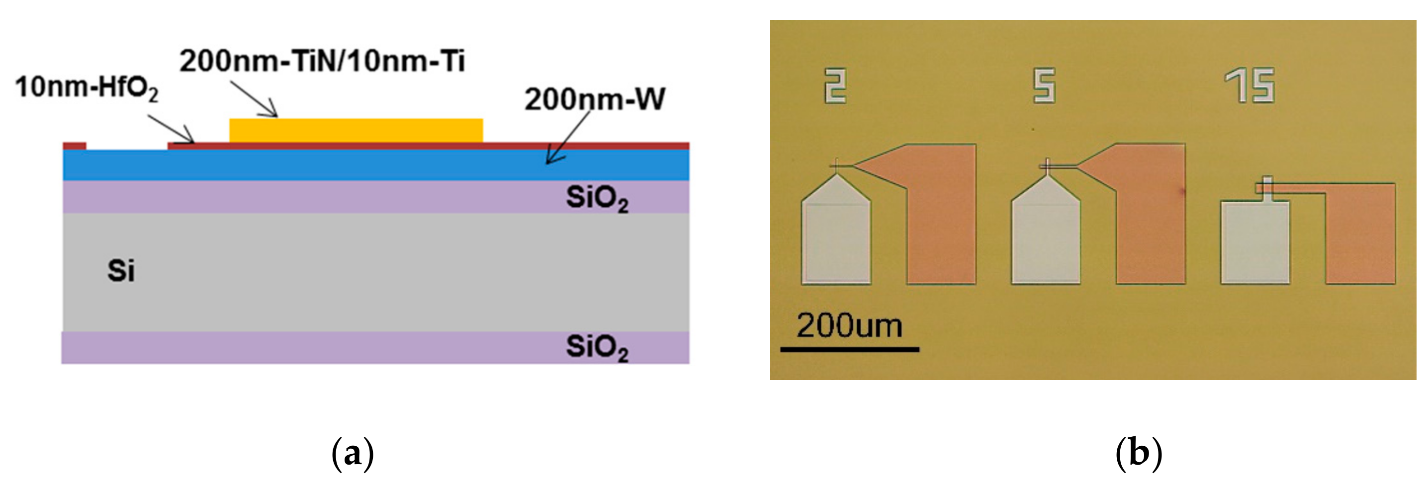
2. Materials and Methods

The RRAM devices used in the experiments are TiN/Ti/HfO2/W structures [17]. The 10 nm-thick HfO2 layer was deposited by atomic layer deposition (ALD) at 225 °C using TDMAH and H2O as precursors. The top and bottom metal electrodes were deposited by magnetron sputtering. The top electrode consists of a 200 nm-TiN and a 10 nm-Ti layer acting as oxygen getter material. The bottom electrode consists of a 200 nm-W layer. Figure 1a shows a schematic cross-section of the device structure. Figure 1b illustrates a top view microscope image of the resulting devices, which are square cells of 15 × 15 μm2, 5 × 5 μm2 and 2 × 2 μm2.
The electrical characterization of the devices under test (DUTs) was performed using a Keysight B2912A Precision Source/Measure Unit (SMU). The instrument was connected to a computer via GPIB (General Purpose Interface Bus) and controlled using MATLAB so that successive measurements were automatically performed. First, the DUTs were electroformed using a positive voltage ramp with a compliance current (ICOMP) of 1 mA. Subsequently, the resistive switching behavior of the DUTs was assessed under DC. The voltage was applied to the top electrode whereas the bottom electrode was grounded, as illustrated in Figure 2a. Double-sweep voltage ramps were applied from 0 to 1.1 V for the SET operation and from 0 to −1.4 V for the RESET operation, as depicted in Figure 2b. Typical resistive-switching characteristics are shown in Figure 3a. As expected, cycle-to-cycle variability is larger in the HRS than in the LRS. The equivalent device resistance was measured during the application of the corresponding SET/RESET voltage ramp when ±0.1 V (±VREAD) was applied between the terminals of the DUT (see Figure 3b).
The laser tests were conducted at the APPLUS laboratories. We mainly used a laser bench with an infrared/IR wavelength available, 1064 nm, with power output up to 2 W. Some experiments were also conducted with two other infrared/IR laser sources: the first one (1024 nm) with a power output up to 5.2 W and the second one (976 nm) with a power output up to 2 W. All the laser sources were with single photon absorption and a nominal pulse width of 100 ns. They were synchronized with the SMU so we could control when the laser pulse was triggered. The default focused laser spot size was 25 μm, but two smaller spots sizes (12 μm and 3 μm) were also considered. A summary about the specifications of the laser sources is found in Table 2.
The laser test was initiated once the proper operation of the RRAM was assessed. The assessment of the operation consisted in 25 cycles composed of a SET and a RESET operation based on the double-sweep voltage ramps reported in Figure 2b. Once the behavior of the DUT was validated, the laser test was conducted with the 1064 nm laser source and a spot size of 25 μm. The attack consisted in applying a laser pulse after the application of a SET operation in order to disrupt the LRS, see Figure 4.a. The resistance state of the RRAM was measured and then a RESET operation was applied. This sequence was repeated 25 times. A similar test was conducted in order to disrupt the HRS (Figure 4b). In this case the laser pulse was applied after a RESET operation. The resistance state of the RRAM was measured and then a SET operation was applied. This sequence was also repeated 25 times.

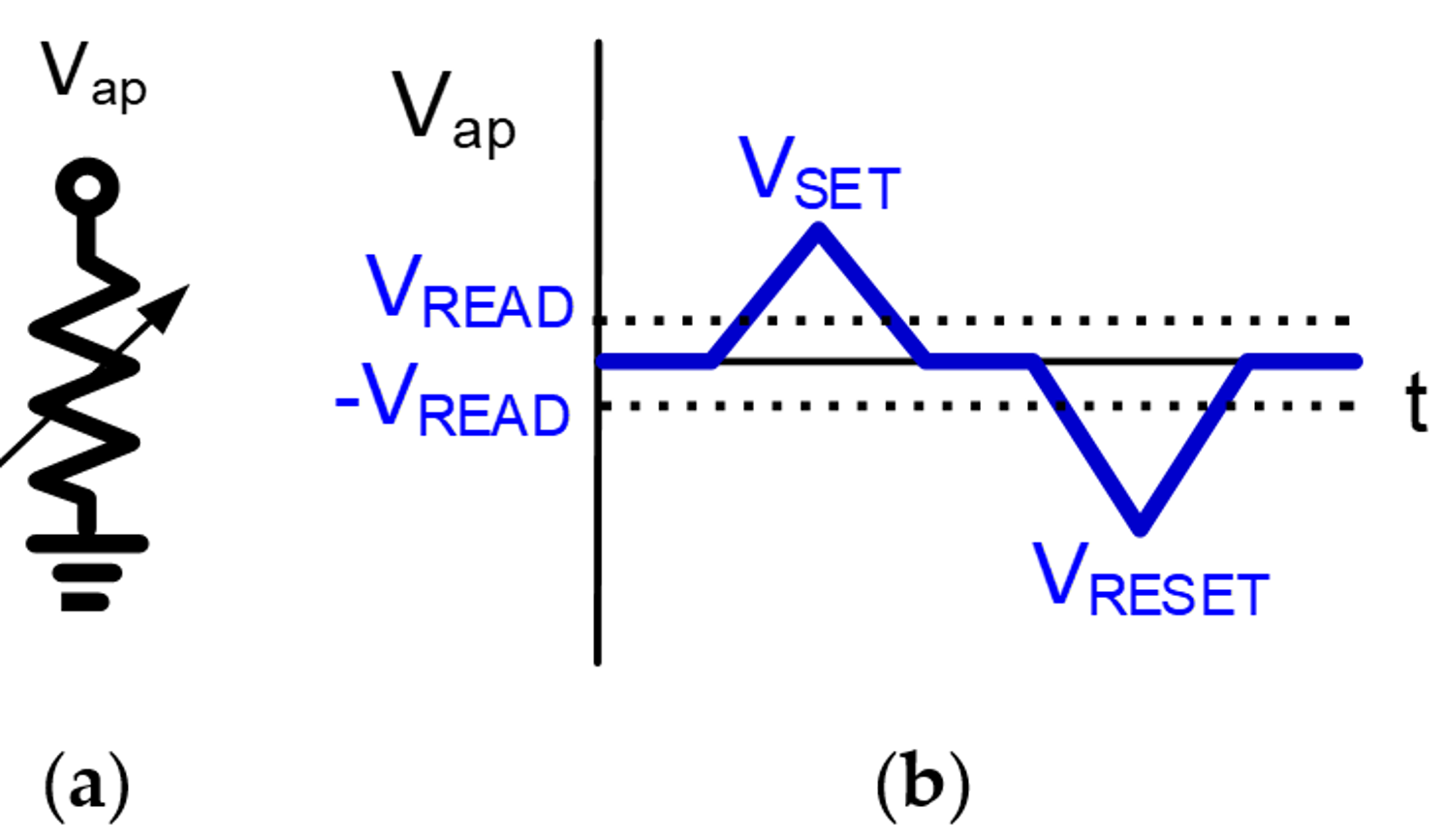
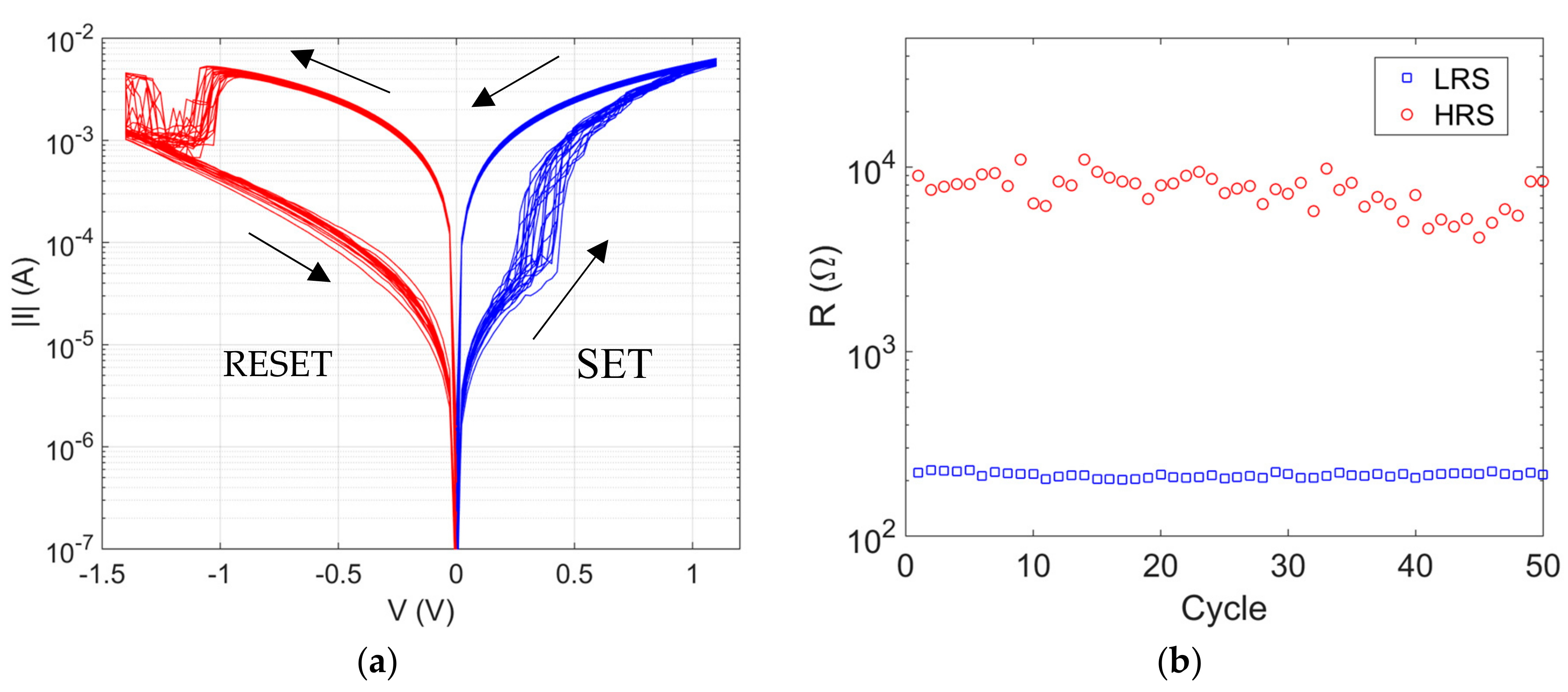
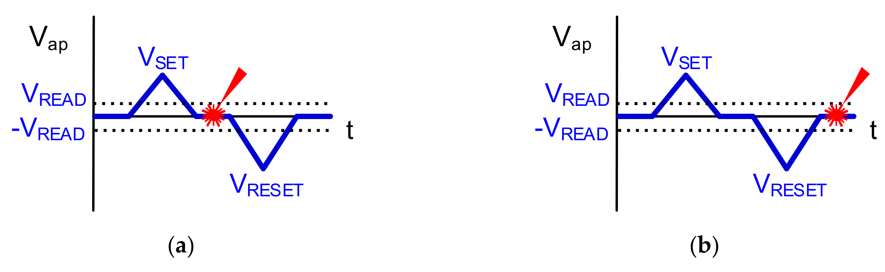
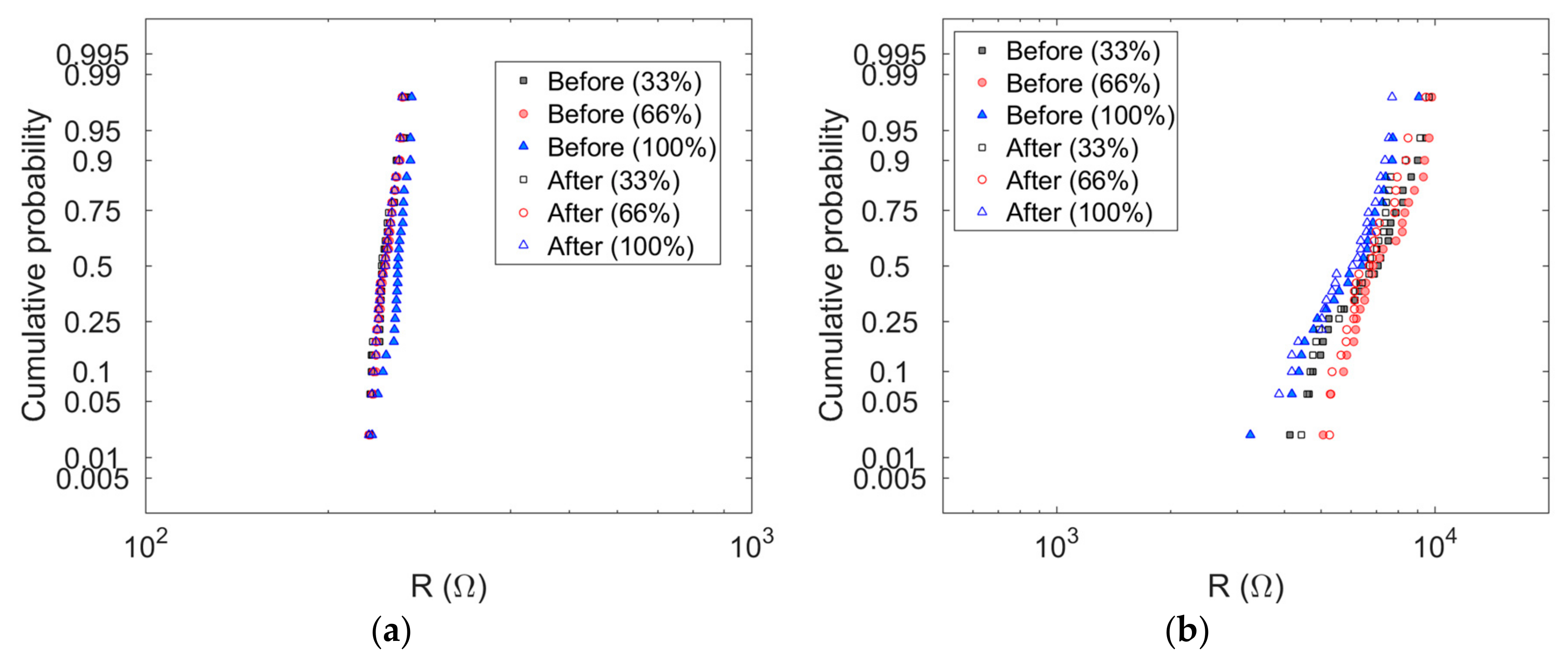
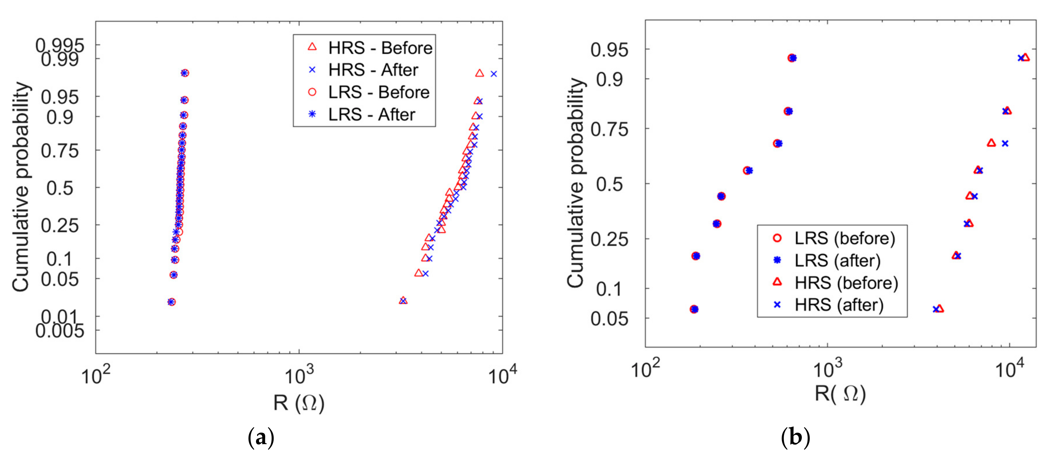
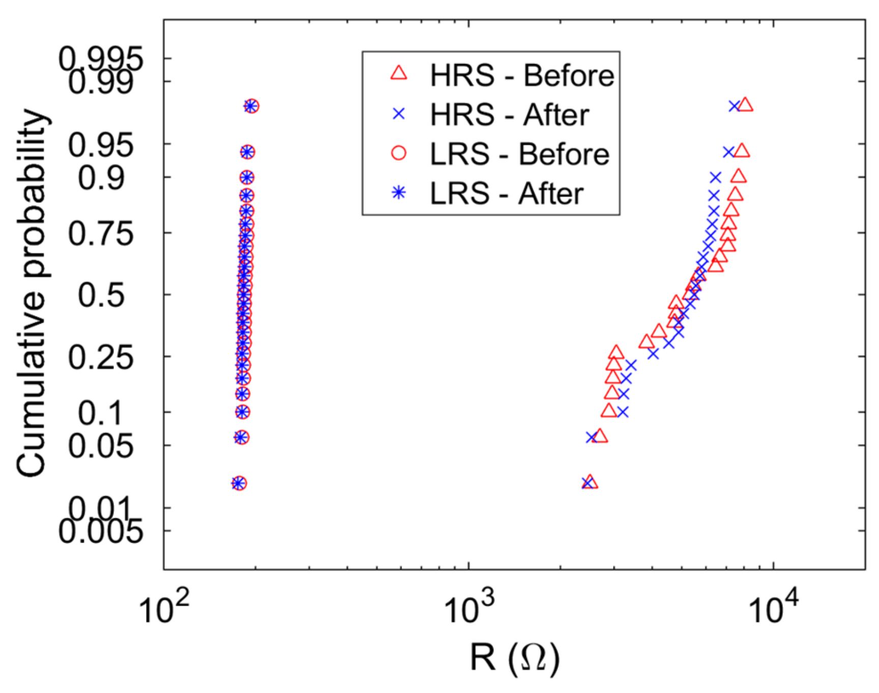
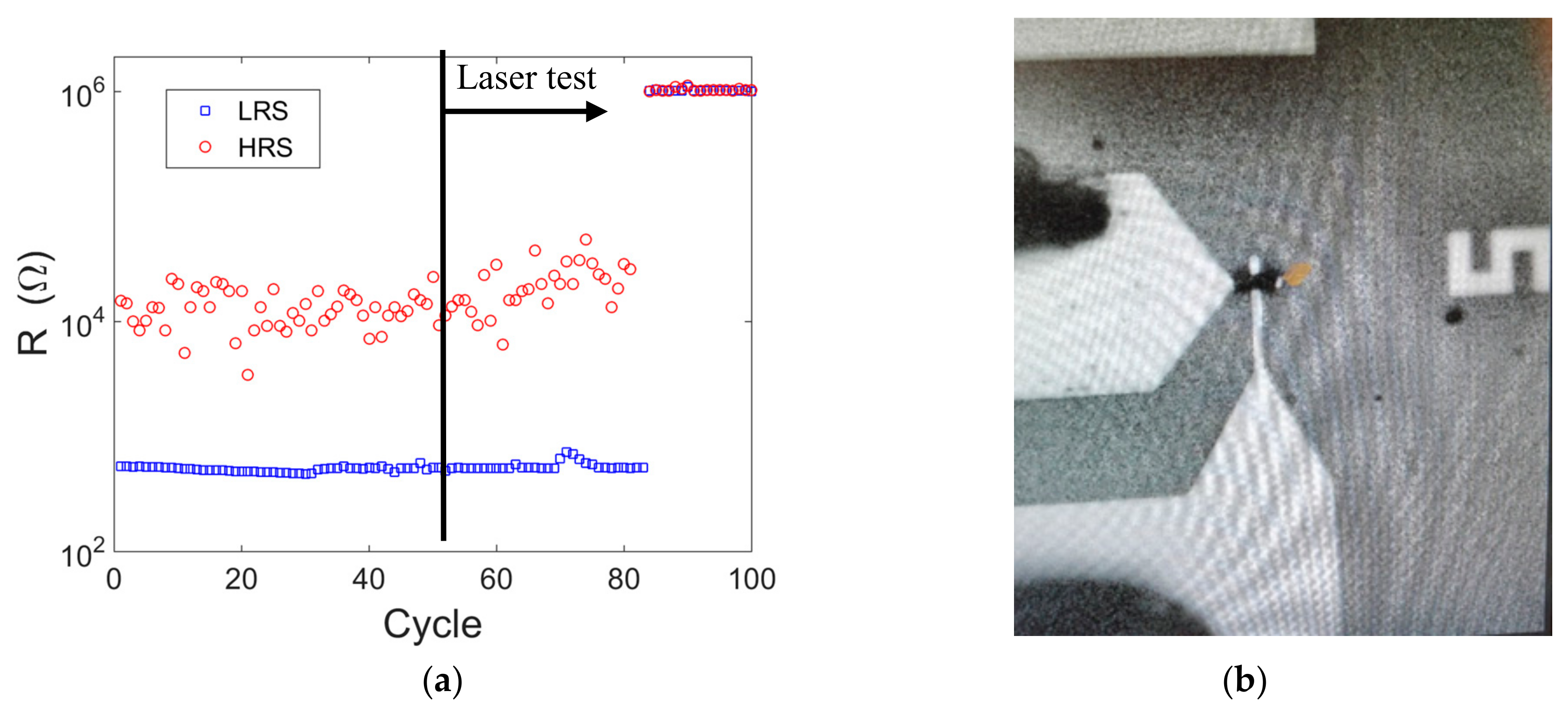
3. Results and Discussion

During the first set of experiments, the laser source (1064 nm) with power output up to 2 W was considered. Different source powers were taken into consideration with a spot size of 25 μm. Figure 5a,b summarize the results when one DUT was irradiated in the LRS and the HRS, respectively, considering different powers of the laser source (33%, 66% and 100%). Although some resistance shifts are observed in the distributions, they can be classified within the range of typical shifts due to the cycle-to-cycle variability. Hence, the laser pulse does not have any noticeable impact on the resistive state of the RRAM regardless of the power source and the resistance state of the device (LRS or HRS). The reversible switching behavior was preserved during the 25 cycles of the experiment. In fact, the DUT still reported the resistive switching behavior after the experiment.
The same tendency was observed for the rest of experiments. From here on, the maximum power of the laser source was always considered. Figure 6a shows the results for another DUT applying a laser pulse during 25 cycles. No noticeable influence of the laser test was observed. Equivalent experiments were conducted with 8 different DUTs of different sizes (2 devices of 2 × 2 μm2, 3 of 5 × 5 μm2 and 3 of 15 × 15 μm2). The cumulative probability is shown in Figure 6b, where the reported resistance at LRS and HRS (before and after applying the laser pulse) is the average resistance during the 25 cycles of the experiment. Results for every specific device are also summarized in Table 3. Although the device-to-device variability is significant at both HRS and LRS, the laser did not influence any of the devices regardless of their size. Subsequently, the initial spot size (25 µm) was decreased to 12 µm to concentrate the power provided by the laser source, but the results for a DUT with 5 × 5 μm2 did not show any observable change, as illustrated in Figure 7. The spot size was reduced to 3 µm with a DUT of 2 × 2 μm2, but the results did not report any significant variation, as shown in Figure 8. Experiments were also conducted with the other infrared/IR laser sources available, the first one (1024 nm) with power output up to 5.2 W and the second one (976 nm) with power output up to 2 W. The maximum power for each laser source was considered during these experiments and, similar to the results with the initial laser source (1064 nm), no significant impact on the resistive state of the devices was observed. It must be pointed out that sweeping the initial pulse width of the laser source (100 ns) up to 3 µs did not induce a fault on the DUT either.
Finally, a last experiment was conducted to force a 5 × 5 μm2 DUT to be upset by the laser source (1024 nm). 50 double-sweep (SET and RESET) voltage ramps were initially applied without laser pulse. Subsequently, another 50 double-sweep voltage ramps were applied with the laser pulse in-between. In this case, the laser source was configured to the Continuous-Wave (CW) mode to release energy continuously during the application of the 50 cycles. The measured resistance of the device during every cycle is reported in Figure 9a. Typical switching behavior is observed during the first 50 cycles, with higher cycle-to-cycle variability in the HRS than the corresponding variability in the LRS. Once the laser pulse was enabled, the switching behavior continued until the DUT was destroyed (around cycle 84). No resistive switching behavior was eventually reported and the DUT remained in a high resistance state, although significantly higher than the one corresponding to the HRS. A photograph of the DUT after the experiment is depicted in Figure 9b. On the cross-point where the device is located a black spot is observed, confirming that the device was burned by the heat. However, it must be mentioned that the device presented several cycles of reversible switching behavior while the laser test was applied, without any fault or transient behavior until the sudden catastrophic failure arose.

4. Conclusions

We investigated the effect of a laser attack on single RRAMs. Experiments were conducted on a set of devices of different sizes. Different conditions were considered during the laser test, modifying the laser source, source power, pulse width, and resistance state of the devices. However, no faults were injected by the different laser tests, although a catastrophic failure was eventually caused when continuous test was applied, destroying the resistive switching behavior of the device. These results are in line with the ones reported in [24], but are different from the ones in [25,26], where, according to the authors, the devices were disturbed in HRS, passing to the LRS after the laser pulse due to a heating effect. The results of the present work can be useful for a better understanding of RRAM devices under the influence of laser attacks. In fact, the discrepancies among the experimental works encourage the continuous research on this area in order to find the most appropriate RRAM devices in terms of dimensions and materials to be resilient against laser attacks and also in order to develop strategies to mitigate the undesirable effects of this attack in RRAM based circuits.

Author Contributions

Conceptualization, D.A., S.M. and R.R.-M., methodology, D.A., S.M., V.M. and D.H.; software, D.A. and Á.G.-P.; validation, D.A. and V.M.; formal analysis, D.A., M.B.G. and F.C.; investigation, D.A., S.M. and V.M.; resources, R.R., D.H., writing—original draft preparation, D.A.; writing—review and editing, Á.G.-P., V.M., M.B.G., F.C.; funding acquisition, F.C. All authors have read and agreed to the published version of the manuscript.

Funding

This research was partially funded by the Spanish Ministry of Science, Innovation and Universities through project TEC2017-84321-C4-1-R, with support of ERDF.

Acknowledgments

This work has made use of the Spanish ICTS Network MICRONANOFABS.

Conflicts of Interest

The authors declare no conflict of interest.

References

  1. Torrezan, A.C.; Strachan, J.P.; Medeiros-Ribeiro, G.; Williams, R.S. Sub-nanosecond switching of a tantalum oxide memristor. Nanotechnology 2011, 22, 5203. [Google Scholar] [CrossRef] [PubMed]
  2. Chen, H.Y.; Yu, S.; Gao, B.; Huang, P.; Kang, J.; Wong, H.-S.P. HfOx based vertical resistive random access memory for cost-effective 3D cross-point architecture without cell selector. In Proceedings of the IEEE International Electron Device Meeting (IEDM), San Francisco, CA, USA, 10–13 December 2012; pp. 20.7.1–20.7.4. [Google Scholar]
  3. Lanza, M. A Review on Resistive Switching in High-k Dielectrics: A Nanoscale Point of View Using Conductive Atomic Force Microscope. Materials 2014, 7, 2155–2218. [Google Scholar] [CrossRef] [PubMed]
  4. Wong, H.-S.P.; Lee, H.-Y.; Yu, S.; Chen, Y.-S.; Wu, Y.; Chen, P.-S.; Lee, B.; Chen, F.T.; Tsai, M.-J. Metal–Oxide RRAM. Proc. IEEE 2012, 100, 1951–1970. [Google Scholar] [CrossRef]
  5. Lim, E.W.; Ismail, R. Conduction Mechanism of Valence Change Resistive Switching Memory: A Survey. Electronics 2015, 4, 586–613. [Google Scholar] [CrossRef]
  6. Yu, S.; Gao, B.; Fang, Z.; Yu, H.Y.; Kang, J.F.; Wong, H.-S.P. Stochastic learning in oxide binary synaptic device for neuromorphic computing. Front. Neurosci. 2013, 7, 186. [Google Scholar] [CrossRef] [Green Version]
  7. Ambrogio, S.; Balatti, S.; Cubeta, A.; Calderoni, A.; Ramaswamy, N.; Ielmini, D. Statistical Fluctuations in HfOx Resistive-Switching Memory: Part I—Set/Reset Variability. IEEE Trans. Electron Devices 2014, 61, 2912–2919. [Google Scholar] [CrossRef] [Green Version]
  8. Grossi, A.; Walczyk, D.; Zambelli, C.; Miranda, E.; Olivo, P.; Stikanov, V.; Feriani, A.; Schoof, G.; Kraemer, R.; Tillack, B.; et al. Impact of Intercell and Intracell Variability on Forming and Switching Parameters in RRAM Arrays. IEEE Trans. Electron Devices 2015, 62, 2502–2509. [Google Scholar] [CrossRef]
  9. Ambrogio, S.; Balatti, S.; Cubeta, A.; Calderoni, A.; Ramaswamy, N.; Ielmini, D. Statistical Fluctuations in HfOx Resistive-Switching Memory: Part II—Random Telegraph Noise. IEEE Trans. Electron Devices 2014, 61, 2920–2927. [Google Scholar] [CrossRef]
  10. González-Cordero, G.; González, M.B.; Campabadal, F.; Jiménez-Molinos, F.; Roldán, J.B. A new technique to analyze RTN signals in resistive memories. Microelectron. Eng. 2019, 215. [Google Scholar] [CrossRef]
  11. Rajendran, J.; Rose, G.S.; Karri, R.; Potkonjak, M. Nano-PPUF: A memristor-based security primitive. In Proceedings of the IEEE Computer Society Annual Symposium on VLSI 2012, Amherst, MA, USA, 19–21 August 2012; pp. 84–87. [Google Scholar] [CrossRef] [Green Version]
  12. Chen, A. Utilizing the variability of resistive Random Access Memory to implement reconfigurable physical unclonable functions. IEEE Electron Device Lett. 2015, 36, 138–140. [Google Scholar] [CrossRef]
  13. Liu, R.; Wu, H.; Pang, Y.; Qian, H.; Yu, S. Experimental characterization of physical unclonable function based on 1 kb Resistive Random Access Memory arrays. IEEE Electron Device Lett. 2015, 36, 1380–1383. [Google Scholar] [CrossRef]
  14. Mazady, A.; Rahman, M.T.; Forte, D.; Anwar, M. Memristor PUF—A Security Primitive: Theory and Experiment. IEEE J. Emerg. Sel. Top. Circuits Syst. 2015, 5, 222–229. [Google Scholar] [CrossRef]
  15. Pang, Y.; Wu, H.; Gao, B.; Deng, N.; Liu, R.; Yu, S.; Chen, A.; Qian, H. Optimization of RRAM-based physical unclonable function with a novel differential read-out method. IEEE Electron Device Lett. 2017, 38, 168–171. [Google Scholar] [CrossRef]
  16. Govindaraj, R.; Ghosh, S.; Katkoori, S. Design, Analysis and Application of Embedded Resistive RAM based Strong Arbiter PUF. IEEE Trans. Dependable Secur. Comput. 2018. [Google Scholar] [CrossRef]
  17. Arumí, D.; Gonzalez, M.B.; Campabadal, F. RRAM serial configuration for the generation of random bits. Microelectron. Eng. 2017, 178, 76–79. [Google Scholar] [CrossRef] [Green Version]
  18. Arumí, D.; Gómez-Pau, Á.; Manich, S.; Rodríguez-Montañés, R.; González, M.B.; Campabadal, F. Unpredictable Bits Generation Based on RRAM Parallel Configuration. IEEE Electron Device Lett. 2019, 40, 341–344. [Google Scholar] [CrossRef]
  19. Lee, G.S.; Kim, G.H.; Kwak, K.; Jeong, D.S.; Ju, H. Enhanced Reconfigurable Physical Unclonable Function Based on Stochastic Nature of Multilevel Cell RRAM. IEEE Trans. Electron Devices 2019, 66, 1717–1721. [Google Scholar] [CrossRef]
  20. Huang, C.Y.; Shen, W.C.; Tseng, Y.H.; King, Y.C.; Lin, C.J. A Contact-Resistive Random-Access-Memory-Based True Random Number Generator. IEEE Electron Device Lett. 2012, 33, 1108–1110. [Google Scholar] [CrossRef]
  21. Balatti, S.; Ambrogio, S.; Carboni, R.; Milo, V.; Wang, Z.; Calderoni, A.; Ramaswamy, N.; Ielmini, D. Physical unbiased generation of random numbers with coupled resistive switching devices. IEEE Trans. Electron Devices 2016, 63, 2029–2035. [Google Scholar] [CrossRef] [Green Version]
  22. Sahay, S.; Kumar, A.; Parmar, V.; Suri, M. OxRAM RNG Circuits Exploiting Multiple Undesirable Nanoscale Phenomena. IEEE Trans. Nanotechnol. 2017, 16, 560–566. [Google Scholar] [CrossRef]
  23. Govindaraj, R.; Ghosh, S.; Katkoori, S. CSRO-Based Reconfigurable True Random Number Generator Using RRAM. IEEE Trans. Very Larg. Scale Integr. Syst. 2018, 26, 2661–2670. [Google Scholar] [CrossRef]
  24. Bennett, W.G.; Hooten, N.C.; Schrimpf, R.D.; Reed, R.A.; Mendenhall, M.H.; Alles, M.L.; Bi, J.; Zhang, E.X.; Linten, D.; Fantini, A.; et al. Single- and Multiple-Event Induced Upsets in HfO2/Hf 1T1R RRAM. IEEE Trans. Nucl. Sci. 2014, 61, 1717–1725. [Google Scholar] [CrossRef]
  25. Krakovinsky, A.; Bocquet, M.; Wacquez, R.; Coignus, J.; Deleruyelle, D.; Djaou, C.; Reimbold, G.; Portal, J.M. Impact of a laser pulse on HfO2-based RRAM cells reliability and integrity. In Proceedings of the 2016 International Conference on Microelectronic Test Structures (ICMTS), Yokohama, Japan, 28–31 March 2016; pp. 152–156. [Google Scholar] [CrossRef]
  26. Krakovinsky, A.; Bocquet, M.; Wacquez, R.; Coignus, J.; Portal, J.M. Thermal laser attack and high temperature heating on HfO2-based OxRAM cells. In Proceedings of the 2017 IEEE 23rd International Symposium on On-Line Testing and Robust System Design (IOLTS), Thessaloniki, Greece, 3–5 July 2017; pp. 85–89. [Google Scholar] [CrossRef] [Green Version]
  27. Mehonic, A.; Gerard, T.; Kenyon, A. Light-activated resistance switching in SiOx RRAM devices. J. Appl. Phys. Lett. 2017, 111, 233502. [Google Scholar] [CrossRef]
  28. Kai, X.; Feng, Z.; Jin, L.; Lanlong, J.; Cong, F.; Jing, L.; Ming, L.; Jinshun, B. Pulsed-laser testing for single event effects in a stand-alone resistive random access memory. In Proceedings of the 2017 IEEE 24th International Symposium on the Physical and Failure Analysis of Integrated Circuits (IPFA), Chengdu, China, 4–7 July 2017; pp. 1–4. [Google Scholar] [CrossRef]
  29. Bi, J.; Han, Z. Mitigation of soft errors in resistive switching random-access-memories. In Proceedings of the 2014 IEEE International Conference on Electron Devices and Solid-State Circuits, Chengdu, China, 18–20 June 2014; pp. 1–2. [Google Scholar] [CrossRef]
Figure 1. (a) Schematic device cross-section; and (b) Top view optical microscope image.
Electronics 09 00200 g001
Figure 2. (a) Schematic device measurement configuration; and (b) Diagram of the applied voltage ramps.
Electronics 09 00200 g002
Figure 3. (a) DC resistive switching behavior during successive SET and RESET operations; and (b) High resistance state (HRS) and low resistance state (LRS) extracted from the DC resistive switching behavior.at −0.1 V and +0.1 V, respectively.
Electronics 09 00200 g003
Figure 4. Laser test (a) With the device in LRS and (b) With the device in HRS.
Electronics 09 00200 g004
Figure 5. Cumulative distributions of the resistance values for a RRAM (15 × 15 μm2) before and after a single laser pulse (spot size of 25 μm)., sweeping the power source value (a) RRAM in the LRS (b) RRAM in the HRS.
Electronics 09 00200 g005
Figure 6. Cumulative distributions (a) of the resistance values for a single RRAM (15 × 15 μm2) before and after a single laser pulse; and (b) of the average resistance for 8 RRAMs of different sizes (152 devices of 2 × 2 μm2, 3 of 5 × 5 μm2 and 3 of 15 × 15 μm2) before and after a single laser pulse. The spot size is 25 μm.
Electronics 09 00200 g006
Figure 7. Cumulative distributions of the resistance values for a single RRAM (5 × 5 μm2) before and after a single laser pulse for different spot sizes (a) RRAM in the LRS; and (b) RRAM in the HRS.
Electronics 09 00200 g007
Figure 8. Cumulative distributions of the resistance values for a single RRAM (2 × 2 μm2) before and after a single laser pulse. The spot size is 3 μm.
Electronics 09 00200 g008
Figure 9. (a) Equivalent resistance for a RRAM during the experiment where the laser source released energy continuously; and (b) Photograph of the RRAM after the experiment.
Electronics 09 00200 g009
Table 1. Comparison of RRAM devices irradiated by a laser source.
WorkStructureDimensions
(nm)
Size
(µm × µm)
CellResults
[24]TiN/Hf/HfO2/TiN?2/10/5/?2105 × 1201T1RHRS to LRS transitions when the transistor is irradiated
[25]TiN/Ti/HfO2/TiN50/10/5/103 × 31RHRS to LRS transitions
[26]Ti/HfO2/TiN10/10/1013 × 311T1RHRS to LRS transitions
[28]?2/HfOx/?2?2/?2/?2?21T1RTransitions when peripheral circuits are irradiated
This workTiN/Ti/HfO2/W200/10/10/2002 × 2
5 × 5
15 × 15
1RNo transitions
1 Not explicitly reported, 2 Data not reported.
Table 2. Information about the laser sources considered in this work.
Laser SourceTypeMaximum Power (W)Wavelenght (nm)Spot Size (µm)
1single photon absorption210643, 12 and 25
25.21024
32976
Table 3. Average resistance for 8 RRAMs of different sizes before and after a single laser pulse.
DUTSize
(µm × µm)
RLRS-Before
(Ω)
RLRS-After
(Ω)
RHRS-Before
(Ω)
RHRS-After
(Ω)
12 × 218518779459436
25 × 563764812,19911,532
35 × 552954151035205
415 × 1518919097039510
55 × 560461741203939
62 × 236337159865840
715 × 1526125960636424
815 × 1524824567046850

