Article

A Power-Efficient Pipelined ADC with an Inherent Linear 1-Bit Flip-Around DAC

1
Beijing Embedded System Key Lab, Faculty of Information Technology, Beijing University of Technology, Beijing 100124, China
2
Beijing Institute of Collaborative Innovation, Beijing 100094, China
*
Authors to whom correspondence should be addressed.
Electronics 2020, 9(1), 199; https://doi.org/10.3390/electronics9010199
Submission received: 19 December 2019 / Revised: 17 January 2020 / Accepted: 19 January 2020 / Published: 20 January 2020
(This article belongs to the Special Issue Low-Voltage Integrated Circuits Design and Application)

Abstract

:
An unity-gain 1-bit flip-around digital-to-analog converter (FADAC), without any capacitor matching issue, is proposed as the front-end input stage in a pipelined analog-to-digital converter (ADC), allowing an input signal voltage swing up to be doubled. This large input swing, coupled with the inherent large feedback factor (ideally β = 1) of the proposed FADAC, enables a power-efficient low-voltage high-resolution pipelined ADC design. The 1-bit FADAC is exploited in a SHA-less and opamp-sharing pipelined ADC, exhibiting 12-bit resolution with an input swing of 1.8 Vpp under a 1.1 V power supply. Fabricated in a 0.13-μm CMOS process, the prototype ADC achieves a measured signal-to-noise plus distortion ratio (SNDR) of 66.4 dB and a spurious-free dynamic range (SFDR) of 76.7 dB at 20 MS/s sampling rate. The ADC dissipates 5.2 mW of power and occupies an active area of 0.44 mm2. The measured differential nonlinearity (DNL) is +0.72/−0.52 least significant bit (LSB) and integral nonlinearity (INL) is +0.84/−0.75 LSB at a 3-MHz sinusoidal input.

1. Introduction

Analog-to-digital converters (ADCs) with above 12-bit resolution and sampling frequency above tens of MHz are widely used in modern communications, instrumentation, and high-quality consumer electronics. Pipeline converters are still attractive in these Nyquist sampling applications that require a combination of high resolution and high throughput [1,2,3,4,5,6,7,8]. For example, pipelined ADCs can be good candidates for OFDM-based 5G systems [9], enabling high speed communications such as virtual reality, remote sensing, needed by a fifth generation (5G) cellular network [10]. Power-efficient and high-performance pipelined ADCs are largely required and play a fundamental role. With the scaling of CMOS technology, the operational speeds of ADCs can be improved due to a high device cute-off frequency. Unfortunately, the significant reduction in the supply voltage and various short-channel effects experienced in these deep-submicron processes create both fundamental and practical design limitations, including lower the achievable amplifier gain, signal voltage swing and enhanced noise level. These limitations lead to a tremendous decrease in the ADC performances, especially if the supply voltage is scaled below 1.2 V [11]. The input signal power of the ADCs is strictly limited due to the reduced supply voltages. Thus the required SNDR of a high resolution ADC necessitates large-size sampling capacitors at the input stage. Meanwhile, the typical implementation of high resolution pipelined ADC requires high-gain and wide-bandwidth operational amplifier (opamp), and excellent capacitor matching in front-end stages. Especially in the input stage, the required accuracy is usually realized at the expense of high power consumption and design complexity [12]. The low-power high resolution pipelined ADC design becomes a great challenge in low voltage deep sub-micron CMOS technology.
Improving input voltage swing proves to be effective to lower the power consumption [13,14]. The larger input signal power can relax the ADC circuit noise requirement, which leads to tolerable amplifier input referred noise, lower sampling capacitor size and thus less loading capacitances during residue amplifier settling. In addition, the larger input swing offers a higher tolerance to opamp and comparator offset, and in turn helps to simplify the circuit design and reduce the power further. In this paper, a doubled input voltage swing under low voltage supply is enabled in an unity-gain 1-bit flip-around digital-to-analog converter (FADAC) at the input stage of pipelined ADC. The large feedback factor and improved SNR in the proposed FADAC result in a power efficient high resolution ADC design.
This paper presents the realization of a low-voltage 0.13-μm CMOS, 12-bit, 20 MS/s ADC. The proposed FADAC is incorporated into a SHA-less and opamp-sharing pipelined architecture [15,16,17,18]. A simple digital foreground calibration is applied to compensate the carry transition error of the 1-bit FADAC [19,20,21]. The prototype 12-bit 20 MS/s pipelined ADC, operating with 1.8 Vpp full-swing input at a 1.1-V supply, achieves a peak signal-to-noise plus distortion ratio (SNDR) of 66.4 dB and spurious-free dynamic range (SFDR) of 76.7 dB.
This paper is organized as follows: Section 2 presents the circuit configuration and operation of the 1-bit FADAC. Section 3 describes the prototype ADC design in detail, followed by the measurement results demonstrated in Section 4. Lastly, Section 5 concludes this paper.

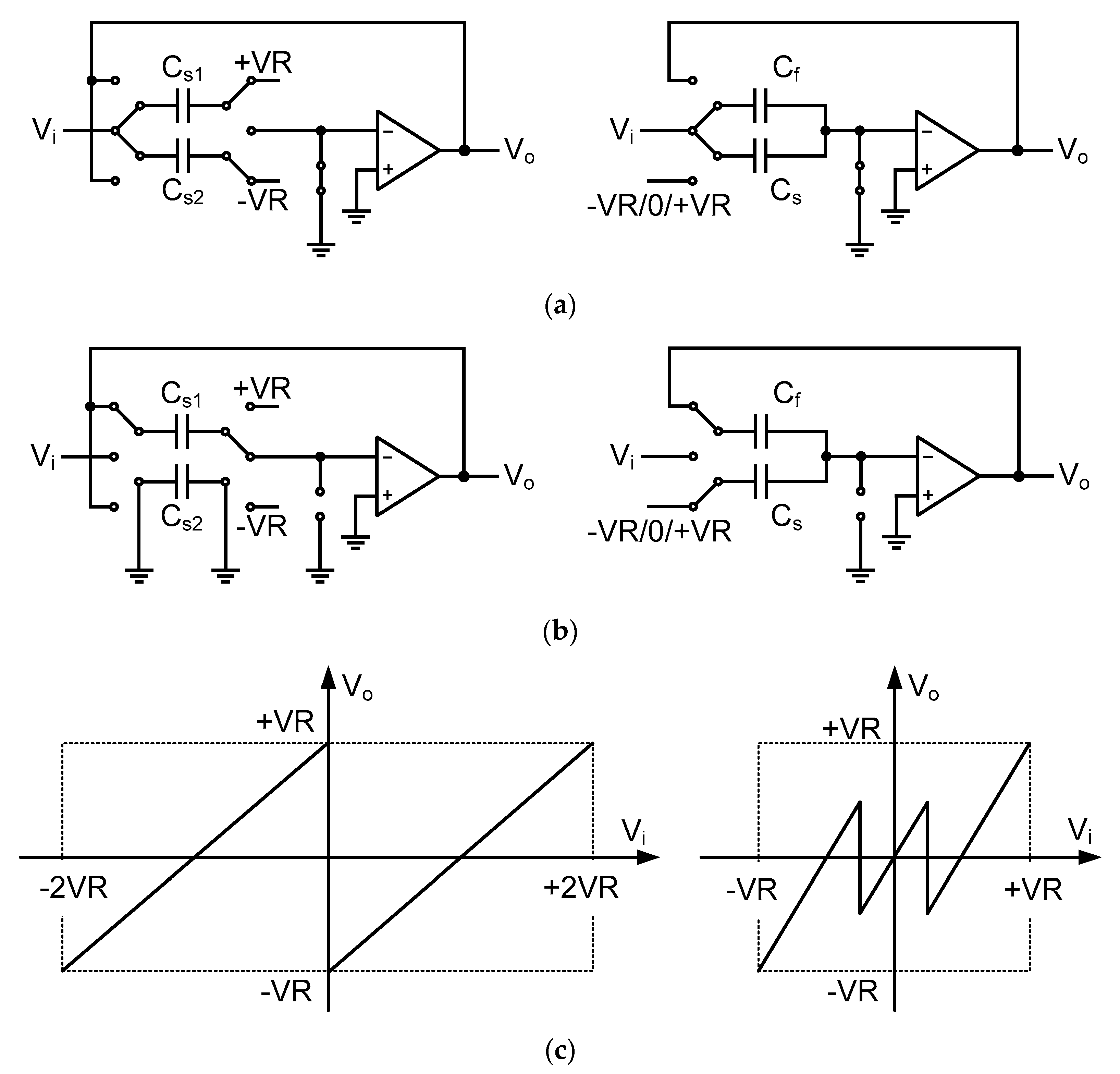
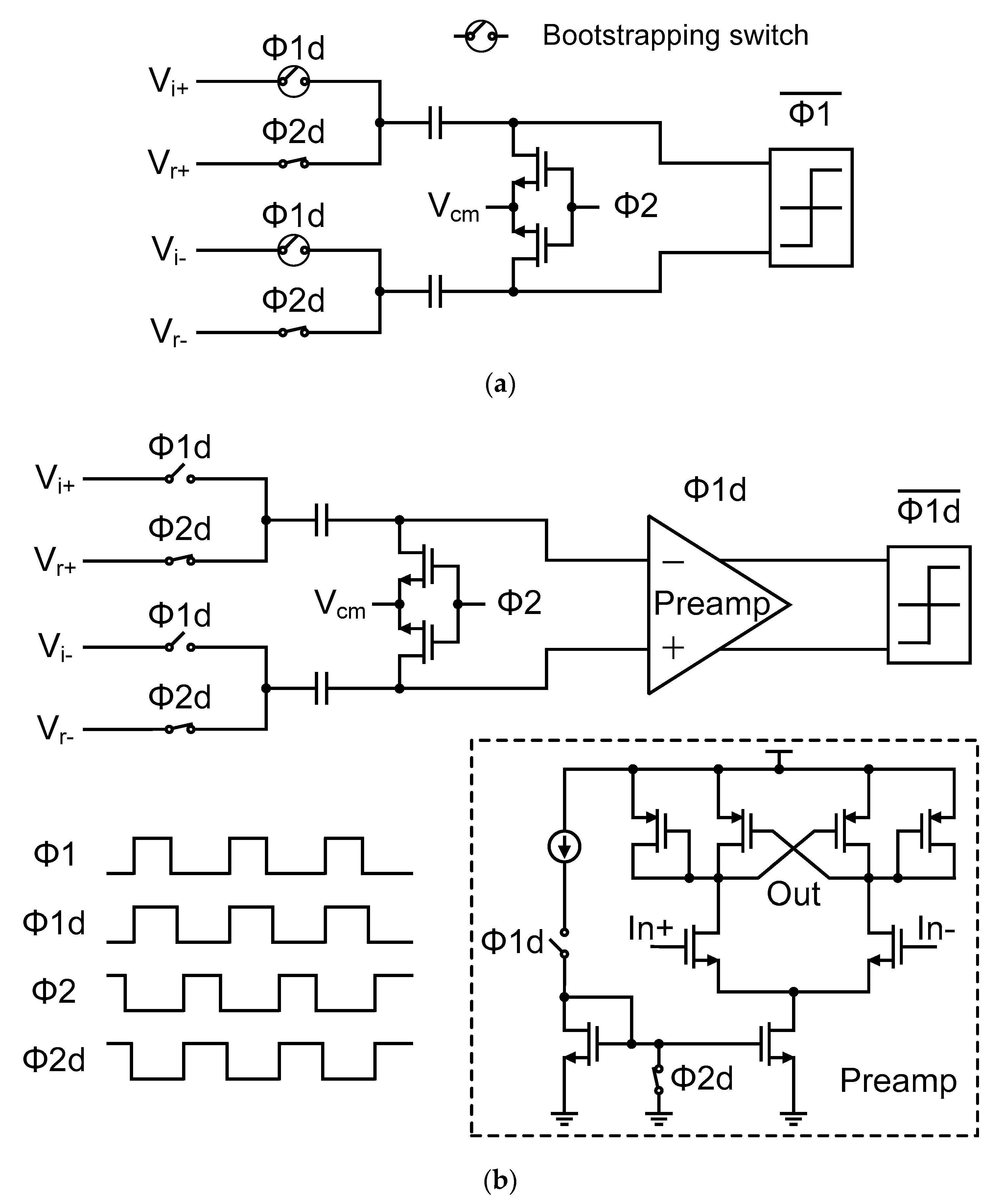
2. Front-end Unity-Gain 1-Bit FADAC

2.1. Unity-Gain 1-Bit FADAC

The proposed FADAC is utilized in the input stage. The operation is similar to the input 1.5-bit multiplying DAC (MDAC) as in a conventional pipelined ADC [3,14,18,19]. Figure 1a,b show the configuration of well-known 1.5-bit MDAC (right in the figure) and the proposed 1-bit FADAC (left in the figure). The operating of 1.5-bit MDAC is based on the charge redistribution on the two capacitors Cs and Cf, and provides a gain of 2 during the hold phase. The gain accuracy depends critically on the matching of these two capacitors. The 1-bit FADAC flips the selected one of the two sampling capacitors to the output, and the gain of 1 is perfectly set during the hold phase, without any capacitor matching requirement. The flipping operation of the capacitor is the same as that in a dedicated flip-around sample-and-hold amplifier (SHA), in which the gain is also ideally 1.
For the ADC with resolution of 12 bit and above, the sampling capacitor matching strictly limited the ADC conversion linearity. Large size capacitors and complicated layout are necessary in 1.5-bit MDAC, so as to improve the capacitor matching. This will lead to larger silicon area occupation and more parasitic capacitance for opamp settling in hold phase, and thus contributes extra power consumption. Compared with 1.5-bit MDAC, the 1-bit FADAC suffers free from the capacitor mismatch issue. As a result, the proposed FADAC can use smaller-size sampling capacitance and save power effectively.
Neglecting parasitic capacitance at the opamp’s summing nodes, the ideal feedback factor of the 1.5-bit MDAC is equal to 0.5, while that of the 1-bit FADAC is 1. The transfer functions of both architectures are plotted in Figure 1c. The unity gain of the FADAC accommodates a large input voltage swing. With identical voltage references for each, the full-scale input range of the 1-bit FADAC is twice as large as the 1.5-bit MDAC, while both maintain the same output range. Thanks to the large feedback factor and the double-increased input voltage swing, the 1-bit FADAC can achieve lower power consumption and higher SNR than the 1.5-bit MDAC. Since the feedback factor of the 1-bit FADAC is twice as high, theoretically the FADAC just needs only 50% of opamp gain-bandwidth product (GBW) to achieve the same closed-loop bandwidth, which results in significant power saving. The performance comparison of 1.5-bit MDAC and 1-bit FADAC is listed and summarized in Table 1.

2.2. Noise Performance Analysis and Compaison

The 1-bit FADAC has the advantages of lower noise than 1.5-bit MDAC. Neglecting parasitic capacitance and assuming all the capacitances in Figure 1 are the same and labeled as C in the following analysis, during the sampling phase as shown in Figure 1a, the input-referred noise power of 1-bit FADAC and 1.5-bit MDAC is the same as v n 2 = ( k T ) / ( 2 C ) . During the hold phase in Figure 1b, the input-referred noise power can be expressed as:
v n 2 = d v n i n 2 G n 2 B W n G s i g 2 ,
where d v n i n 2 is opamp’s input-referred noise power density, G n is the noise gain which is equal to 1 / β , G s i g is the signal gain which is 1 and 2 in 1-bit FADAC and 1.5-bit MDAC respectively, and B W n is the noise bandwidth [22,23]. Assuming that the opamp is a single-stage amplifier and can be modeled as a single-pole system, and the noise is dominated by the input transistors, the input-referred noise power of both can be calculated from Equation (1), and given by:
{ v n i n , F A . 2 = 8 π 3 ( k T C L . F A . ) v n i n , M . 2 = 8 π 6 ( k T C L . M . ) ,
where C L , F A and C L , M are the load capacitance of FADAC and MDAC respectively during hold phase. It can be seen that the input-referred noise power of 1-bit FADAC, v n i n , F A 2 , is almost twice as high as the noise power of 1.5-bit MDAC, v n i n , M 2 . However, the input signal power of FADAC is 4 times higher; so the 1-bit FADAC can obtain a 3-dB SNR improvement.
It should be noted that the overall ADC’s noise contribution not only depends on the input stage, but also the following front-end stages, especially when the input stage resolves low resolution most significant bits (MSBs). In order to compare the noise performance of both architectures in a fair way, assuming that there are two same-resolution ADCs with utilizing 1-bit FADAC and 1.5-bit MDAC as input stage respectively, the noise performance of each ADCs can be compared in a simply way. Because both FADAC and MDAC have decided 1-bit MSB, and the output residue signal has identical full range and the same remaining resolution bits to be further resolved, thus the design requirement of the following stages-2 to the end in respective ADC is exactly the same, and the noise of these stages referred to the input of stage-2, which is also the output of the input stage, is the same. The noise performance of each ADC is easy to be decided by comparing the total noise referred to the output of the input stage. The signal power at this node is the same, and the referred noise to this node can be divided into two parts. The first is the total input noise contributed by the following stage-2 to the end, which is the same in both ADCs. The second is the output referred noise of the input stage. Noise gain from the input of the FADAC to the output is one, while the gain is doubled in the 1.5-bit MDAC. It can be easily revealed from equation (2) that the output referred noise power of 1.5-bit MDAC is about twice as high [11]. Assuming the first part noise contribution has the same level with the output noise power of FADAC, an overall 2dB-SNR improvement can be obtained in the 1-bit FADAC. In other words, for the same SNR requirement for both ADCs, 1-bit FADAC can adopt sampling capacitors with much smaller size than 1.5-bit MDAC, which will make FADAC easier be driven by the input buffer and also lead to significant power saving for the input buffer.

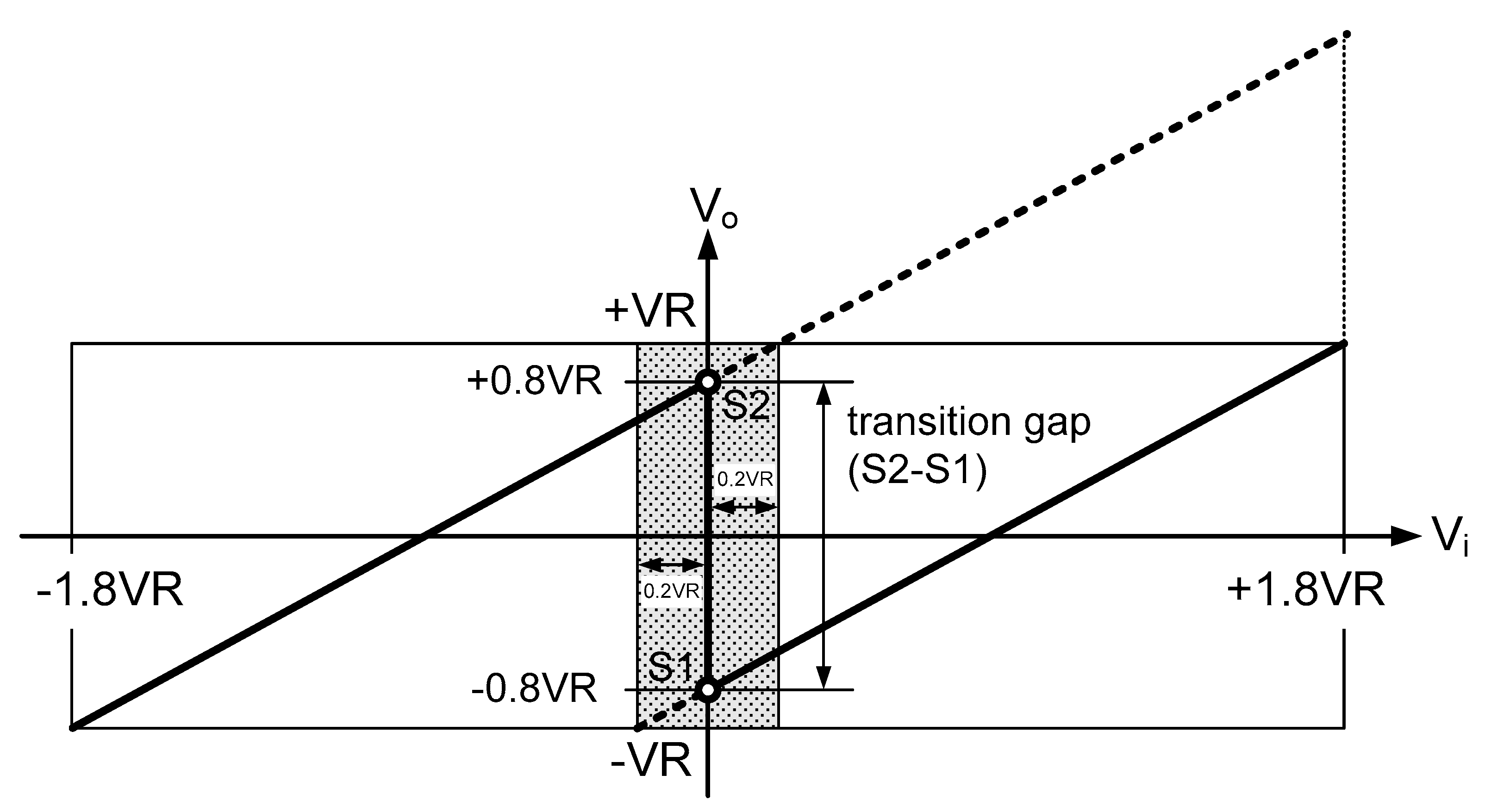
2.3. Digital Foreground Calibration

As shown in Figure 1c, there are two line segments and one transition boundary in the transfer curve of the 1-bit FADAC. The feature of flip-around architecture makes the slopes of both segments equal to ideal one, and the transition position is determined by the decision point of the comparator in the first stage. Missing codes or missing decision levels would happen in practical ADC realization, due to the opamp and comparator offset, charge injection, mismatches between different capacitor paths, etc. These nonidealities vertically shift the transfer plot or change the transition point, which will result in missing codes and missing decision level, and cause analog-to-digital conversion failure.
A practical issue in the 1-bit FADAC is how to resolve or tolerate these nonidealities. Previous works in 1-bit-per-stage ADC make the gain a little bit lower [19], and leave space to the reference boundary at the end point, so as to offer the headroom as the tolerance. However, this tolerance is limited due to the smaller decrement of the gain. Furthermore this will reduce the feedback factor and thus increase the power consumption. In this work, a large tolerance is achieved without decreasing the feedback factor. As shown in Figure 2, a modified transfer function is provided for the proposed 1-bit FADAC. The left line segment is for MSB = 0 and shifted vertically down from VR to 0.8 VR at the transition point, leaving 0.2 VR headroom from the reference boundary. The right line segment is for MSB = 1 and shifted up in the same way. The key of this technique is to make residue output voltage with any offset error still remain within the input full range of the next stage, and thus avoid missing decision levels. A shade region is depicted in Figure 2, and reveals a ±0.2 VR tolerance, which is large enough to cover all the aforementioned nonidealities.
As shown in Figure 2, the carry transition from MSB = 0 to MSB = 1 in the digital domain corresponds to a translation on the y-axis of the right segment in the transfer curve. To preserve the transfer characteristics, the transition gap should be equal to the distance between S1 and S2, which are the end-points of the two segments and labeled in Figure 2. Otherwise, the error of missing codes or nonmonotonic codes will be introduced. A simple digital calibration method is employed to compensate the carry transition error in the 1-bit FADAC. The transition gap of S2 minus S1, denoted as (S2-S1), is measured easily in a foreground manner [19,20,21,23]. The inputs are shorted together, and then MSB is forced to be zero first and next to be one, the ADC outputs of these two points can be stored and the code difference is equal to the transition gap (S2-S1). During the practical conversion, when MSB is zero, the ADC output is final output code. When MSB is one, the outputs of the later stages (stage 2 to the end) are added to (S2-S1) in calibration logic, and the corresponding results are the ADC digital outputs. In this way, missing codes or nonmonotonic codes, the mismatches between different signal paths, imprecision of reference voltages, even with finite opamp gain in the FADAC, all above nonidealities can be calibrated simultaneously in the digital domain. Please note that there is only one transition point required to be calibrated for the overall ADC conversion, thus the hardware cost and power consumption of the calibration are extremely low.

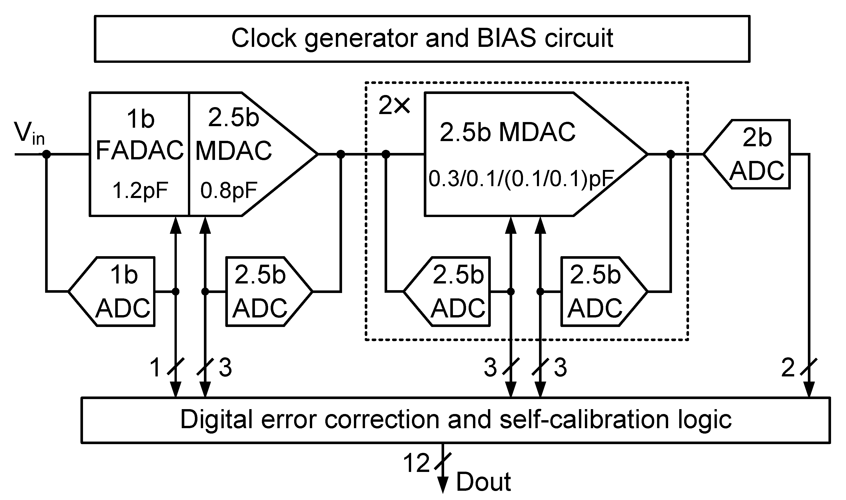
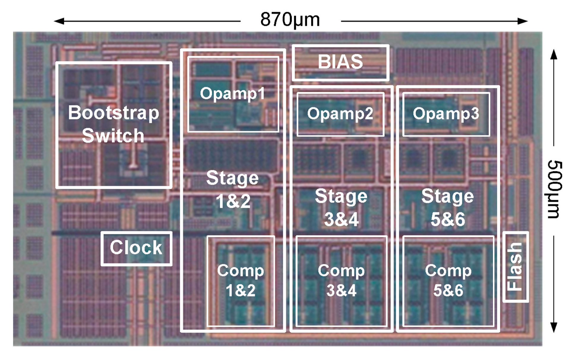
3. Prototype ADC Design

3.1. ADC Architecture
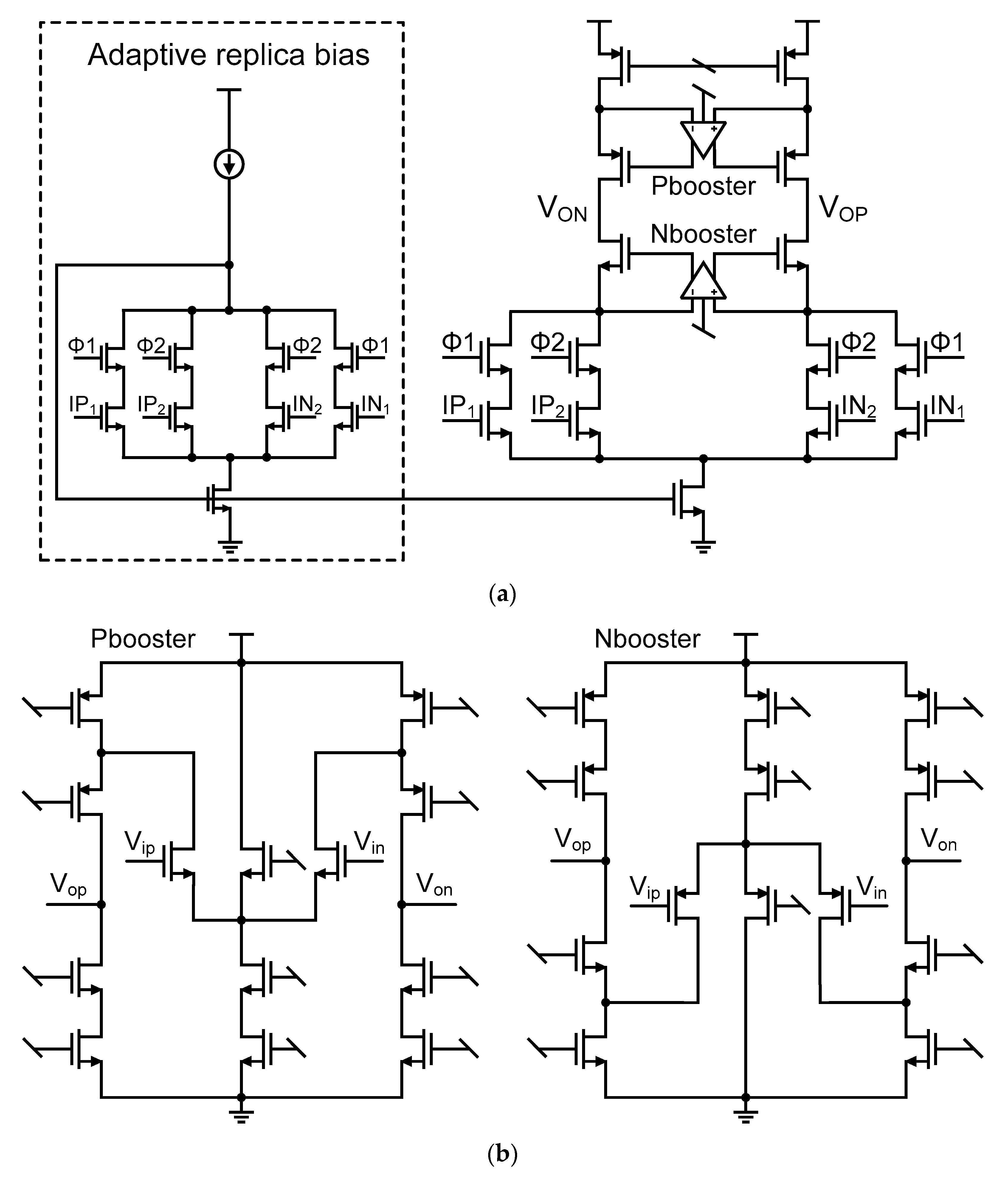
The block diagram of the proposed ADC is shown in Figure 3. The proposed 1-bit FADAC is applied in the first front-end stage of the pipelined ADC. Five 2.5-bit stages and one 2-bit flash ADC are followed as in a conventional pipeline implementation. There are total 17 raw bits from the second stages to the last one. All these raw bits are feed into the digital error correction (DEC) logic. The digital compensation value of transition gap (S2-S1) is measured and stored either. The final 12 bit ADC output digital codes are produced using simple calibration logic. In Figure 3, the capacitance values in each stage are labeled. Stage scaling is utilized to reduce power.
Dedicated SHA is eliminated in the ADC for considering power, area and noise performance [11,15,16]. Thanks to the benefits of the proposed FADAC, the relaxed thermal noise, including not only kT/C thermal noise but also amplifier noise, allows a much smaller sampling capacitor to be used in the front-end 1-bit FADAC. Smaller capacitor in the first stage can ease the settling requirement of input sampling network, also improving the bandwidth to track high frequency input signal. In addition, less parasitic capacitances are introduced, which means less loading capacitance and is helpful for the settling of residue amplifier. In this work, the capacitor of 1.2 pF is selected to sample the analog inputs. As labeled in Figure 3, the sampling capacitor sizes are scaled down along the pipeline to save the power consumption and area occupation.
Opamp-sharing technique is employed in this design to lower power dissipation significantly. As shown in Figure 3, only three opamps are used totally for overall 6 stages. The first opamp is shared by the front-end 1-bit FADAC and the second 2.5-bit MDAC. Due to the much smaller feedback factor of residue amplifier in the 2.5-bit MDAC, the GBW of the first opamp is dominated by the 2.5-bit MDAC. This enables the FADAC obtaining much time margin and being tolerant to the slewing during the opamp settling in the hold phase. The summing node reset problem in conventional opamp-sharing structure is mitigated by utilizing dual-input differential pairs in the amplifier [17], which is shown in Figure 4.

3.2. OPAMP Design

A single-stage telescopic opamp is adopted for the power efficiency. Gain-boosting technique is utilized to achieve large dc gain while maintaining a single-stage frequency response. Figure 4a shows the circuit schematic of the main opamp with dual inputs and the two auxiliary amplifiers as gain boosters as shown in Figure 4b. The inputs of IP1 and IN1 are served as the summing nodes of the first stage, while IP2 and IN2 for the second stage. When Φ1 is high and Φ2 is low, IP1 and IN1 are active in the hold phase of the first stage. At the same time IP2 and IN2 are reset to the opamp input common mode voltage in the sampling phase of the second stage, and vice versa. Since both input pairs are reset alternately and periodically, the memory effect is fully eliminated in this work.
An adaptive replica biasing scheme is exploited in the telescopic opamp. The replica bias and local negative feedback guarantee the large output swing for the residue amplifier. The drain-source voltage of n-type tail current source is adjusted to less than 100 mV, so as to leave more room for the output voltage swing. Considering small parasitics capacitance at the summing node, all the input transistors use almost minimum channel length. In simulation, an 87 dB of dc gain at a 1.1 V supply was observed with a 1 Vpp output swing in the first opamp. The current consumption is dominant by the main opamp. The current, as well as the area, of the replica bias circuit is 15 times less than the main opamp excluding the two booster amplifiers.

3.3. Comparator Design

There is only one comparator in the first stage, which leads to an easier matching between the sampling paths of the FADAC and the comparator. Thus the proposed FADAC input stage can relax the timing skew problem in conventional SHA-less ADC architecture, which is helpful for high frequency input sampling. The circuit schematic of the comparator in the FADAC stage is shown in Figure 5a. A dynamic comparator without front preamplifier is directly used to regenerate the output MSB due to the large offset tolerance in the 1-bit FADAC stage. Bootstrapping switch and bottom plate sampling scheme are adopted to improve the signal path matching with that in FADAC.
In the following 2.5-bit stages, the offset tolerance is limited, so a preamplifier with a voltage gain of 6.5× is added in front of the dynamic latch to reduce the offset of the comparator and lower the kick back noise. In addition, the large number of comparators in five 2.5-bit stages consumes much power. Switched-preamplifier scheme is utilized in this design to reduce the current consumption. With proper clock phase, the preamplifier turn-on delay influence can be neglected. The circuit schematic and the clock phases of the comparator in the 2.5-bit stage are shown in Figure 5b.

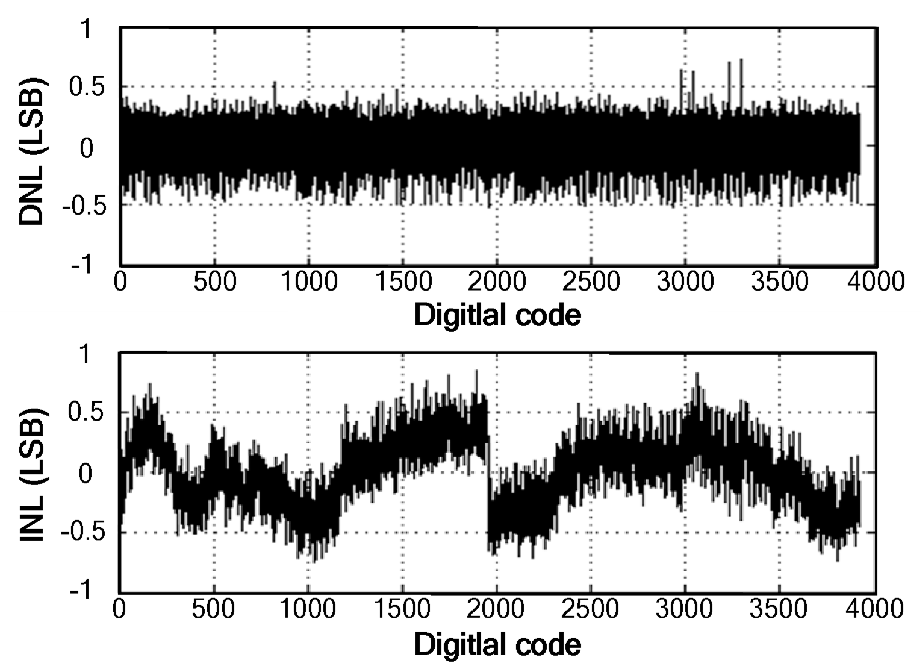
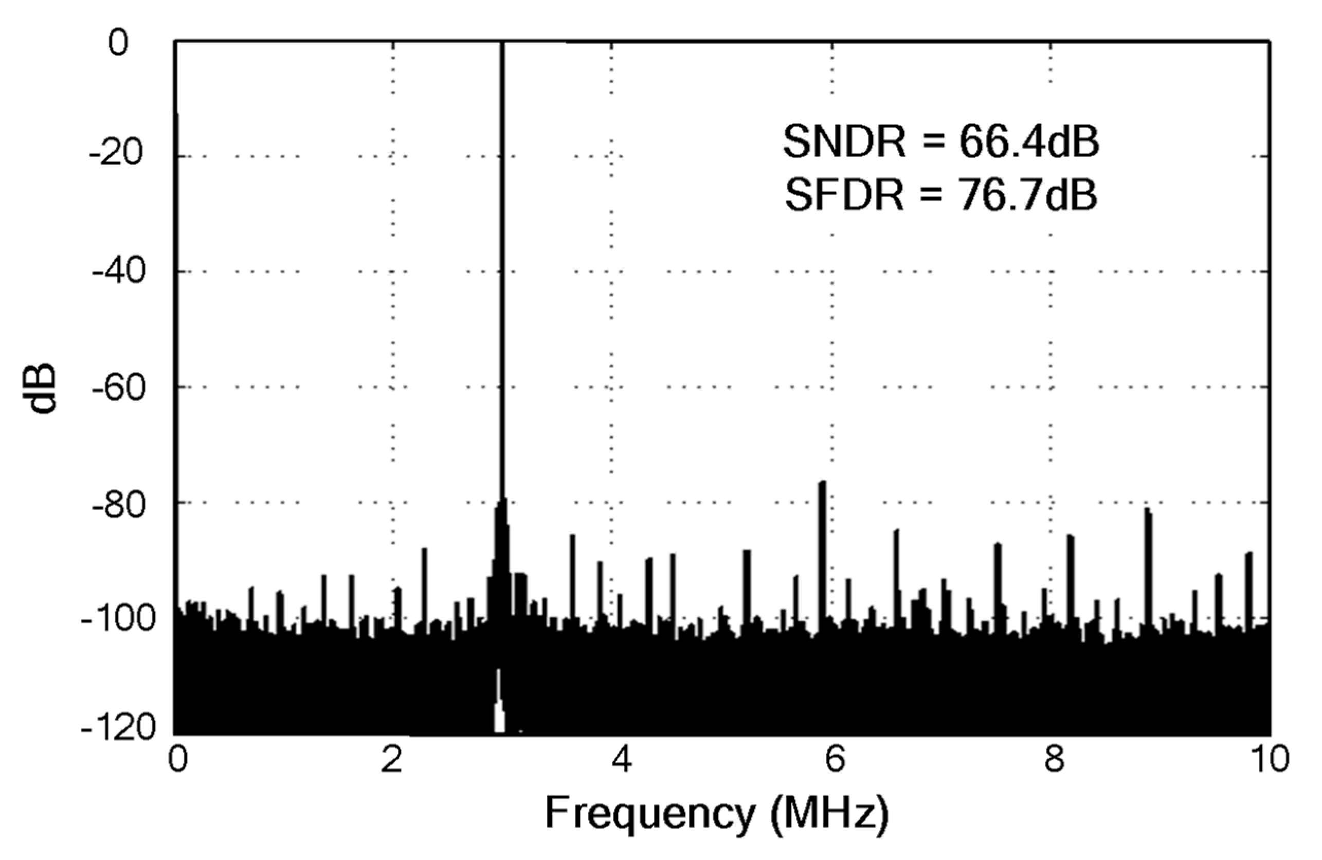
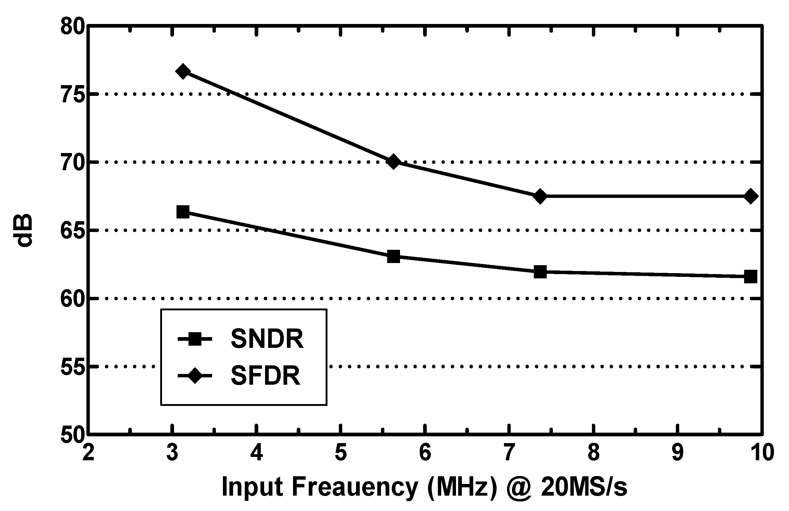
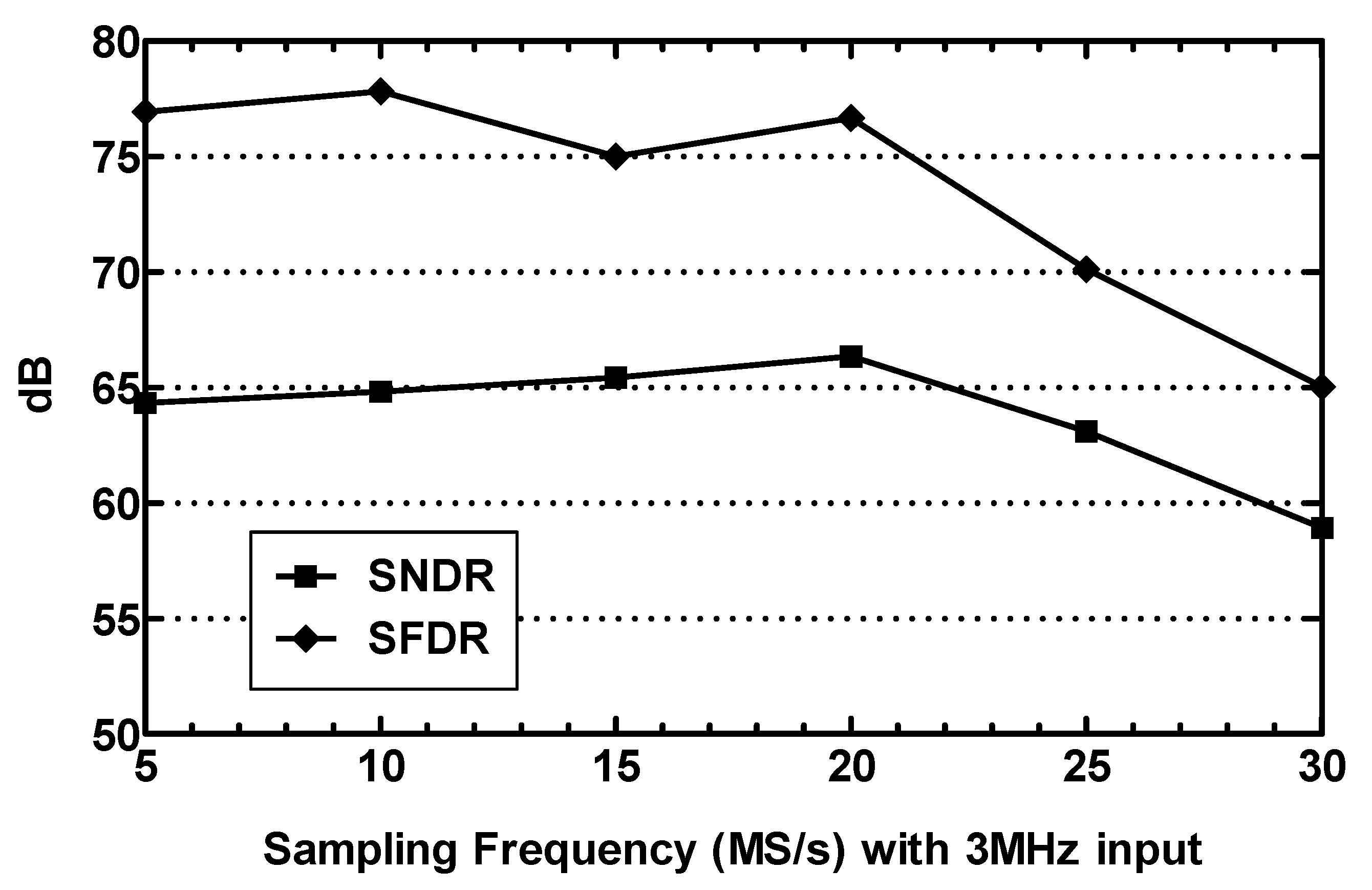
4. Experimental Results

The prototype 12-bit pipelined ADC was fabricated in a 0.13-μm CMOS process. Figure 6 shows the die micrograph of the ADC. The active area is 0.44 mm2. At a 1.1 V power supply, the full-scale input swing is up to 1.8 Vpp. In conventional pipeline ADC design, the typical full-scale input is about 1 Vpp with 1.2 V supply. Figure 7 shows the measured differential nonlinearity (DNL) and integral nonlinearity (INL), which are +0.72/−0.52 LSB and +0.84/−0.75 LSB, respectively.
Figure 8 shows the measured ADC output spectrum plot. The input signal is a 3-MHz input with a −1 dBFS voltage swing. At 20 MS/s sampling rate, the measured signal-to-noise plus distortion ratio (SNDR) is 66.4 dB and spurious-free dynamic range (SFDR) is 76.7 dB. Figure 9 plots the measured SNDR and SFDR versus input frequency at 20 MS/s. When the input frequency is increased close to the Nyquist band edge, the ENOB of over 10 bit has already been achieved. Figure 10 plots the SNDR and SFDR versus sampling frequency with a 3-MHz input. Note that all the above experiment results were obtained with using the identical frozen digital value of transition gap (S2-S1), which is extracted by the digital compensation logic.
The total power consumption is 5.2 mW, including 4.2 mW for clock, bias, FADAC and MDACs, 0.8 mW for all comparators, and estimated 0.2 mW for DEC and calibration logic. The prototype ADC hasled to a FOM (Power/(fs × 2ENOB)) of 153 fJ/conversion-step at low frequency and 254 fJ/conversion-step at Nyquist frequency. The performance summary and comparison with some other ADC works with a similar resolution, sampling rate, and measured SNDR level are provided in Table 2 [24,25,26].

5. Conclusions

In this paper, a 12-bit 20 MS/s pipelined ADC employing the front-end novel 1-bit FADAC is reported. The proposed FADAC has an inherent linear unity-gain, also features a high input voltage swing and large feedback factor. The FADAC is incorporated into a SHA-less and opamp-sharing pipelined ADC, achieving low voltage, low power and high SNDR in a 0.13μm CMOS. The effort on circuit design, including dual-input telescopic opamp for opamp-sharing technique, adaptive replica bias scheme and switched-preamplifier in comparator, enables a power efficient ADC realization. The techniques proposed in this work have good potential for the low power high resolution ADCs in scale CMOS technologies with low supply voltages.

Author Contributions

Conceptualization, P.W.; Funding acquisition, P.W. Investigation, P.W., L.S., H.Z. and Z.C.; Writing—original draft, P.W.; Writing—review & editing, L.S. and Z.C. All authors have read and agreed to the published version of the manuscript.

Funding

This work was supported in part by the National Natural Science Foundation of China under key Grant 61731019, and in part by the Natural Science Foundation of Beijing Municipality under Grant 4184083.

Acknowledgments

The authors would like to thank Skyrelay for the support of silicon fabrication.

Conflicts of Interest

The authors declare no conflicts of interest.

References

  1. Lagos, J.; Hershberg, B.; Martens, E.; Wambacq, P.; Craninckx, J. Asingle-channel 600Msps 12bit ringamp-based pipelined ADC in 28nm CMOS. In Proceedings of the 2017 Symposium on VLSI Circuits, Kyoto, Japan, 5–8 June 2017; pp. C96–C97. [Google Scholar]
  2. Boo, H.H.; Boning, D.S.; Lee, H.S. A 12b 250MS/s pipelined ADC with virtual ground reference buffers. In Proceedings of the 2015 IEEE International Solid-State Circuits Conference, San Francisco, CA, USA, 22–26 February 2015; pp. 282–284. [Google Scholar]
  3. El-Chammas, M.; Li, X.; Kimura, S.; Coulon, J.; Hu, J.; Smith, D.; Landman, P.; Weaver, M. 90dB-SFDR 14b 500MS/S BiCMOS switched-current pipelined ADC. In Proceedings of the 2015 IEEE International Solid-State Circuits Conference, San Francisco, CA, USA, 22–26 February 2015; pp. 286–288. [Google Scholar]
  4. Dolev, N.; Kramer, M.; Murmann, B. A12-Bit,200-MS/s,11.5-mW pipeline ADC using a pulsed bucket brigade front-end. In Proceedings of the 2013 Symposium on VLSI Circuits, Kyoto, Japan, 12–14 June 2013; pp. C98–C99. [Google Scholar]
  5. Oh, T.; Venkatram, H.; Moon, U.K. A70MS/s69.3dBSNDR38.2fJ/conversion-step time-based pipelined ADC. In Proceedings of the 2013 Symposium on VLSI Circuits, Kyoto, Japan, 12–14 June 2013; pp. C96–C97. [Google Scholar]
  6. Mohammad, T.S.; Hamoui, A.A. A reconfigurable and power-scalable10–12 bit0.4–44MS/s pipelined ADC with0.35–0.5pJ/Stepin1.2V90nm digital CMOS. IEEE Trans. Circuits Syst. I Regul. Pap. 2013, 60, 74–83. [Google Scholar]
  7. Yuan, J.; Fung, S.W.; Chan, K.Y.; Xu, R.Y. A12-bit20MS/s56.3mW pipelined ADC with interpolation-based nonlinear calibration. IEEE Trans. Circuits Syst. I Regul. Pap. 2012, 59, 555–565. [Google Scholar] [CrossRef]
  8. Hershberg, B.P.; Weaver, S.T.; Moon, U.K. A 1.4V signal swing hybrid CLS-opamp/ZCBC pipelined ADC using a 300mV output swing opamp. In Proceedings of the 2010 IEEE International Solid-State Circuits Conference, San Francisco, CA, USA, 7–11 February 2010; pp. 302–304. [Google Scholar]
  9. Ponce-Hinestroza, V.Y.; Castaneda-Camacho, J.; Gonzalez-Diaz, V.R.; Mino-Aguilar, G.; Garcia-Santigao, A. Pipelined A/D converter design for 5G OFDM communication systems. In Proceedings of the 2018 IEEE 88th Vehicular Technology Conference (VTC-Fall), Chicago, IL, USA, 27–30 August 2018; pp. 1–5. [Google Scholar]
  10. Huo, Y.; Dong, X.; Xu, W.; Yuen, M. Enabling multi-functional 5G and beyond user equipment: A survey and tutorial. IEEE Access 2019, 7, 116975–117008. [Google Scholar] [CrossRef]
  11. Chiu, Y.; Gray, P.R.; Nikolic, B. A 14-b 12-MS/s CMOS pipelined ADC with over 100-dB SFDR. IEEE J. Solid State Circuit 2005, 39, 2139–2151. [Google Scholar] [CrossRef]
  12. Zhou, Z.K.; Lin, M.; Huang, S.G.; Wang, R.Y.; Dong, Y.M. A 12 bit 120 MS/s SHA-less pipeline ADC with capacitor mismatch error calibration. IEICE Electron. Express 2018, 15, 1–12. [Google Scholar] [CrossRef]
  13. El-Chammas, M.; Li, X.; Kimura, S.; Coulon, J.; Hu, J.; Smith, D.; Landman, P.; Weaver, M. A 10b 125MS/s 40mW Pipelined ADC in 0.18µm CMOS. In Proceedings of the 2015 IEEE International Solid-State Circuits Conference, San Francisco, CA, USA, 6–10 February 2005; pp. 282–283. [Google Scholar]
  14. Yang, C.Y.; Li, F.L.; Li, W.T.; Wang, X.; Wang, Z.H. An 85 mW 14-bit 150MS/s pipelined ADC with 71.3 dB peak SNDR in 130 nm CMOS. In Proceedings of the 2013 Asian Solid State Circuits Conference, Singapore, 11–13 November 2013; pp. 85–86. [Google Scholar]
  15. Huang, P.L.; Hsien, S.K.; Lu, V.; Wan, P.Y.; Lee, S.C.; Liu, W.B.; Chen, B.W.; Lee, Y.P.; Chen, W.T.; Yang, T.Y.; et al. SHA-Less pipelined ADC with in situ background clock-skew calibration. IEEE J. Solid State Circuits 2011, 46, 1893–1903. [Google Scholar] [CrossRef]
  16. Huang, P.L.; Hsien, S.K.; Lu, V.; Wan, P.Y.; Lee, S.C.; Liu, W.B.; Chen, B.W.; Lee, Y.P.; Chen, W.T.; Yang, T.Y.; et al. SHA-less pipelined ADC converting 10th Nyquist band with in-situ clock-skew calibration. In Proceedings of the 2011 Custom Integrated Circuits Conference, San Francisco, CA, USA, 19–22 September 2010; pp. 1–4. [Google Scholar]
  17. Yin, Y.; Wen, X.; Liao, Y.; Zhang, W.; Tang, Z.W. Switch-embedded opamp-sharing MDAC with dual-input OTA in pipelined ADC. IEEE Electron. Lett. 2010, 46, 831–832. [Google Scholar] [CrossRef] [Green Version]
  18. Peng, B.; Huang, G.Z.; Li, H.; Wan, P.Y.; Lin, P. A 48-mW, 12-bit, 150-MS/s pipelined ADC with digital calibration in 65 nm CMOS. In Proceedings of the 2011 Custom Integrated Circuits Conference, San Francisco, CA, USA, 19–21 October 2011; pp. 1–4. [Google Scholar]
  19. Karanicolas, A.N.; Lee, H.; Bacrania, K.L. A 15-b 1-Msample/s digitally self-calibrated pipeline ADC. IEEE J. Solid State Circuits 1993, 28, 1207–1215. [Google Scholar] [CrossRef] [Green Version]
  20. Zhong, J.Y.; Zhu, Y.; Chan, C.H.; Sin, S.W.; Seng-Pan, U.; Martins, R.P. A12b180MS/s0.068 mm2 with full-calibration-integrated pipelined-SARADC. IEEE Trans. Circuits Syst. I Regul. Pap. 2017, 64, 1684–1695. [Google Scholar] [CrossRef]
  21. Huang, H.; Du, L.; Chiu, Y. A1.2-GS/s8-bit two-stepSARADCin65-nmCMOS with passive residue transfer. IEEE J. Solid State Circuits 2017, 52, 1551–1562. [Google Scholar] [CrossRef]
  22. Yang, W.; Kelly, D.; Mehr, L.; Sayuk, M.T.; Singer, L. A 3-V 340-mW 14-b 75-Msample/s CMOS ADC with 85-dB SFDR at Nyquist input. IEEE J. Solid State Circuits 2001, 36, 1931–1936. [Google Scholar] [CrossRef]
  23. Li, J.; Guo, X.; Luan, J.; Wu, D.; Zhou, L.; Huang, Y.; Wu, N.; Jia, H.; Zheng, X.; Wu, J.; et al. A 3G 12-bit four-channel time-interleaved pipelined ADC in 40 nm CMOS process. Electronics 2019, 8, 1551. [Google Scholar] [CrossRef] [Green Version]
  24. Ahmed, I.; Johns, D.A. An 11-bit 45 MS/s pipelined ADC with rapid calibration of DAC errors in a multibit pipeline stage. IEEE J. Solid State Circuits 2008, 43, 1626–1637. [Google Scholar] [CrossRef] [Green Version]
  25. Sasidhar, N.; Kook, Y.J.; Takeuchi, S.; Hamashita, K.; Takasuka, K.; Hunumolu, P.K.; Moon, U.K. A 1.8V 36-mW 11-bit 80MS/s pipelined ADC using capacitor and opamp sharing. In Proceedings of the 2007 IEEE Asian Solid-State Circuits Conference, Jeju, Korea, 12–14 November 2007; pp. 241–243. [Google Scholar]
  26. Treichler, J.; Huang, Q.T. A 11.1-bit ENOB 50-MS/s pipelined A/D converter in 130-nm CMOS without S/H front end. In Proceedings of the 2010 IEEE European Solid-State Circuits Conference, Sevilla, Spain, 13–17 September 2010; pp. 374–377. [Google Scholar]
Figure 1. (a) Sampling phase; (b) Hold phase; (c) Transfer curve for 1-bit FADAC (left) and 1.5-bit MDAC (right).
Electronics 09 00199 g001
Figure 2. Transfer curve of the proposed 1-bit FADAC.
Electronics 09 00199 g002
Figure 3. ADC block diagram.
Electronics 09 00199 g003
Figure 4. (a) Dual-input single-stage telescopic opamp with adaptive biasing; (b) Booster amplifiers.
Electronics 09 00199 g004
Figure 5. (a) Comparator in the first stage; (b) Comparator in the following stages.
Electronics 09 00199 g005
Figure 6. ADC die micrograph.
Electronics 09 00199 g006
Figure 7. Measured DNL and INL.
Electronics 09 00199 g007
Figure 8. Measured output spectrum at 20MS/s with a 3-MHz input.
Electronics 09 00199 g008
Figure 9. Measured SNDR and SFDR vs. input frequency.
Electronics 09 00199 g009
Figure 10. Measured SNDR and SFDR vs. sampling frequency.
Electronics 09 00199 g010
Table 1. Performance comparison for 1.5-bit MDAC and 1-bit FADAC.
Parameters1.5-Bit MDAC1-Bit FADAC
Resolved bit11
Ideal feedback factor β0.51
Opamp GBW requirement1 ×0.5 ×
Gain accuracy≈2 (Cs and Cf matching issue)Perfect unity gain
Input full swing2 VR4 VR
SNR/~3dB improved
Table 2. Performance summary and comparison.
Parameters[6][7][8][14][18][24][25][26]This Work
ArchitecturePipe.Pipe.Pipe.Pipe.Pipe.Pipe.Pipe.Pipe.Pipe.
Resolution (bit)121112141211111412
Sample rate (MS/s)44202015015045805020
Max. DNL (LSB)0.90.27/0.80.30.451.3/0.72
Max. INL (LSB)1.260.2/2.61.01.13.11/0.84
Peak SNDR (dB)65.172.568.371.36760.153.271.466.4
Peak SFDR (dB)7984.476.393.6817066.790.576.7
Power (mW)22.956.317.285488138109.55.2
FoM1 1 @ low fin/78040513819421791206991153
FoM2 @ high fin350/528188////254
CMOS technology90 nm0.35 µm0.18 µm0.13 µm65 nm0.18 µm0.18 µm0.13 µm0.13 µm
Supply voltage (V)1.23.31.41.31.21.81.81.21.1
Active area (mm2)120.641.1110.783.572.163.430.44
1 FoM(fJ/conversion-step).

