Cost-Effective 4 GHz VCO Using Only Miniature Spirals Realized in a 0.18 μm CMOS Process for Wireless Sensor Network (WSN) Applications


Abstract
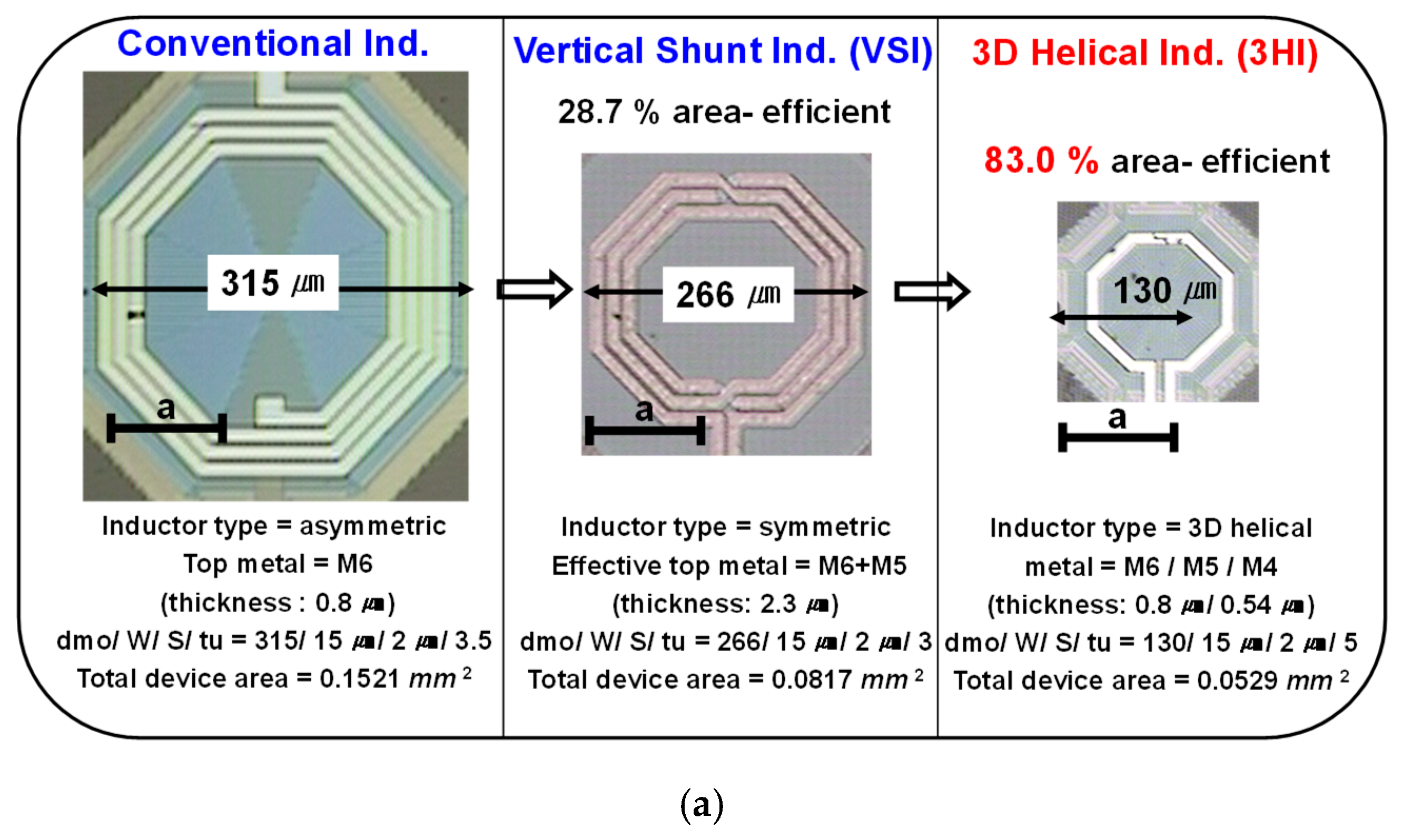
:1. Introduction
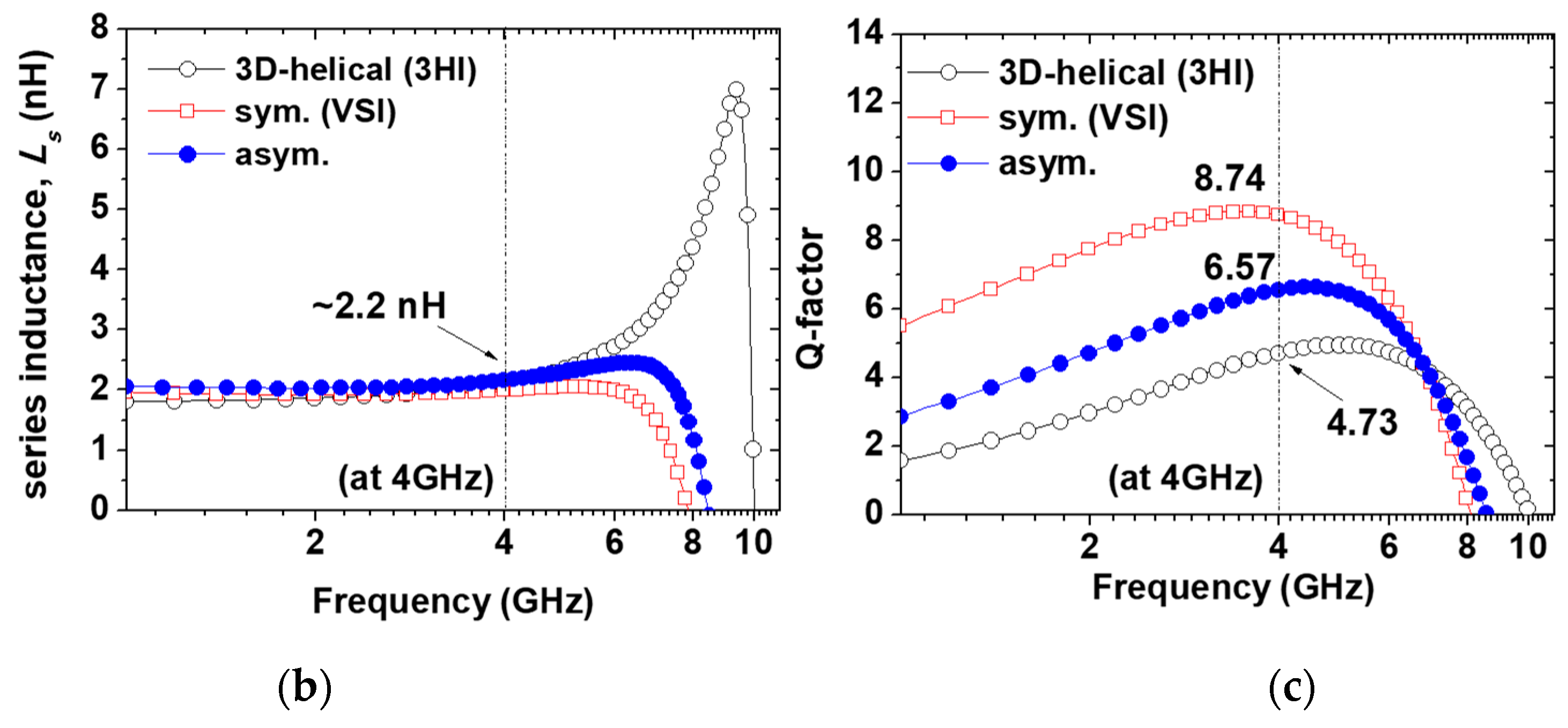
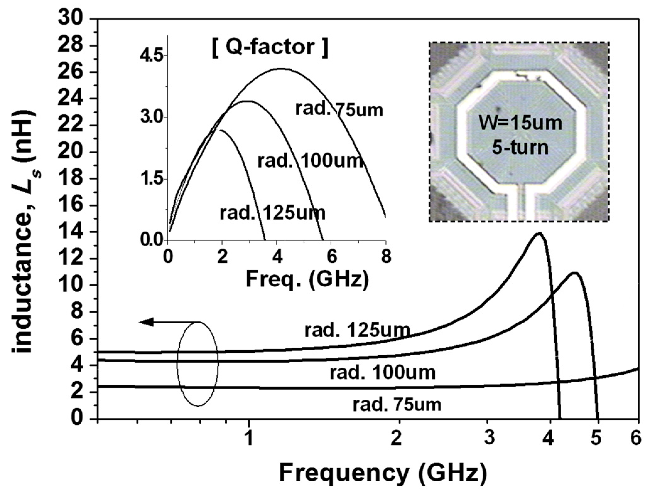
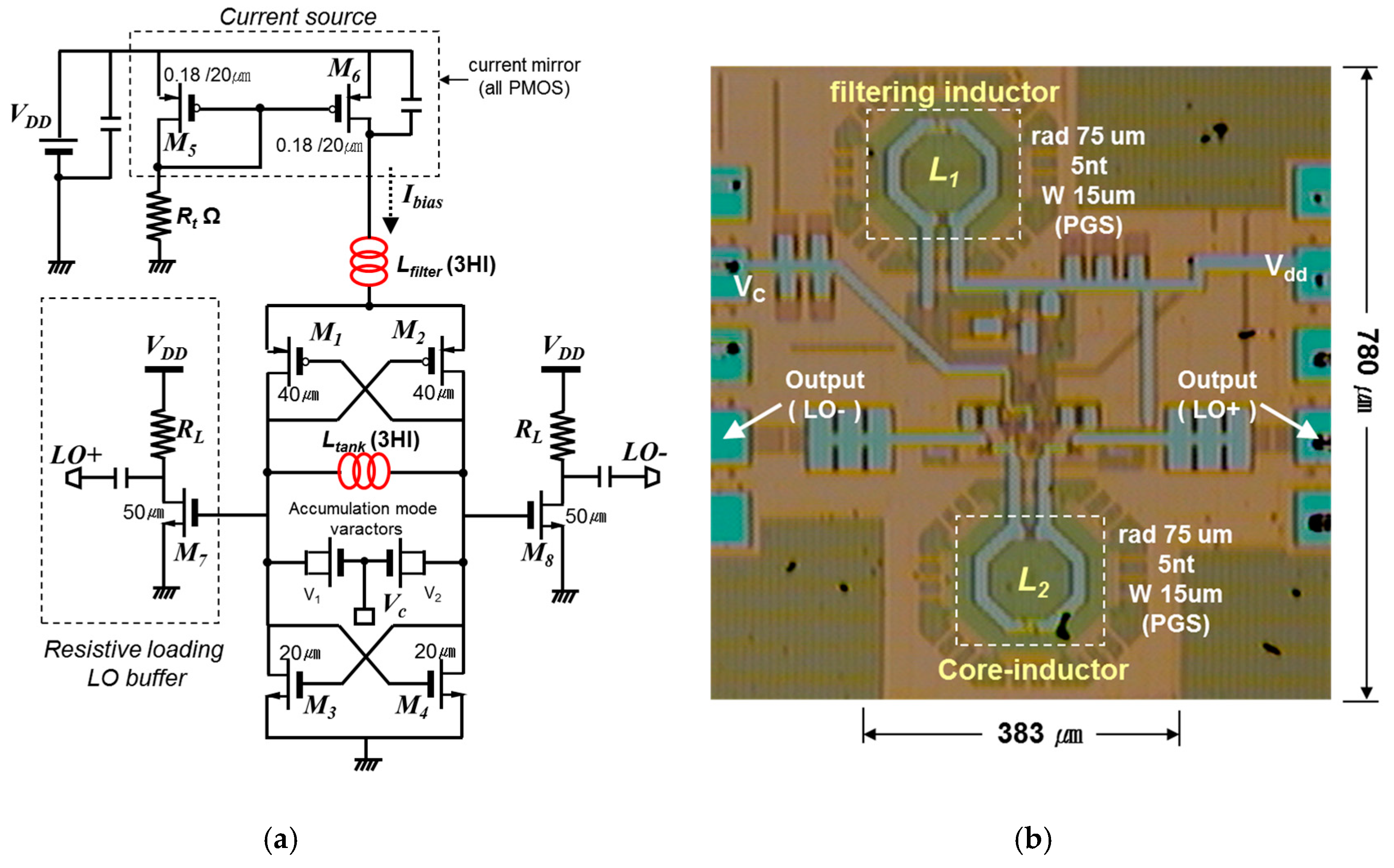
2. Extreme Cost-Effective LC-VCO Circuit Design
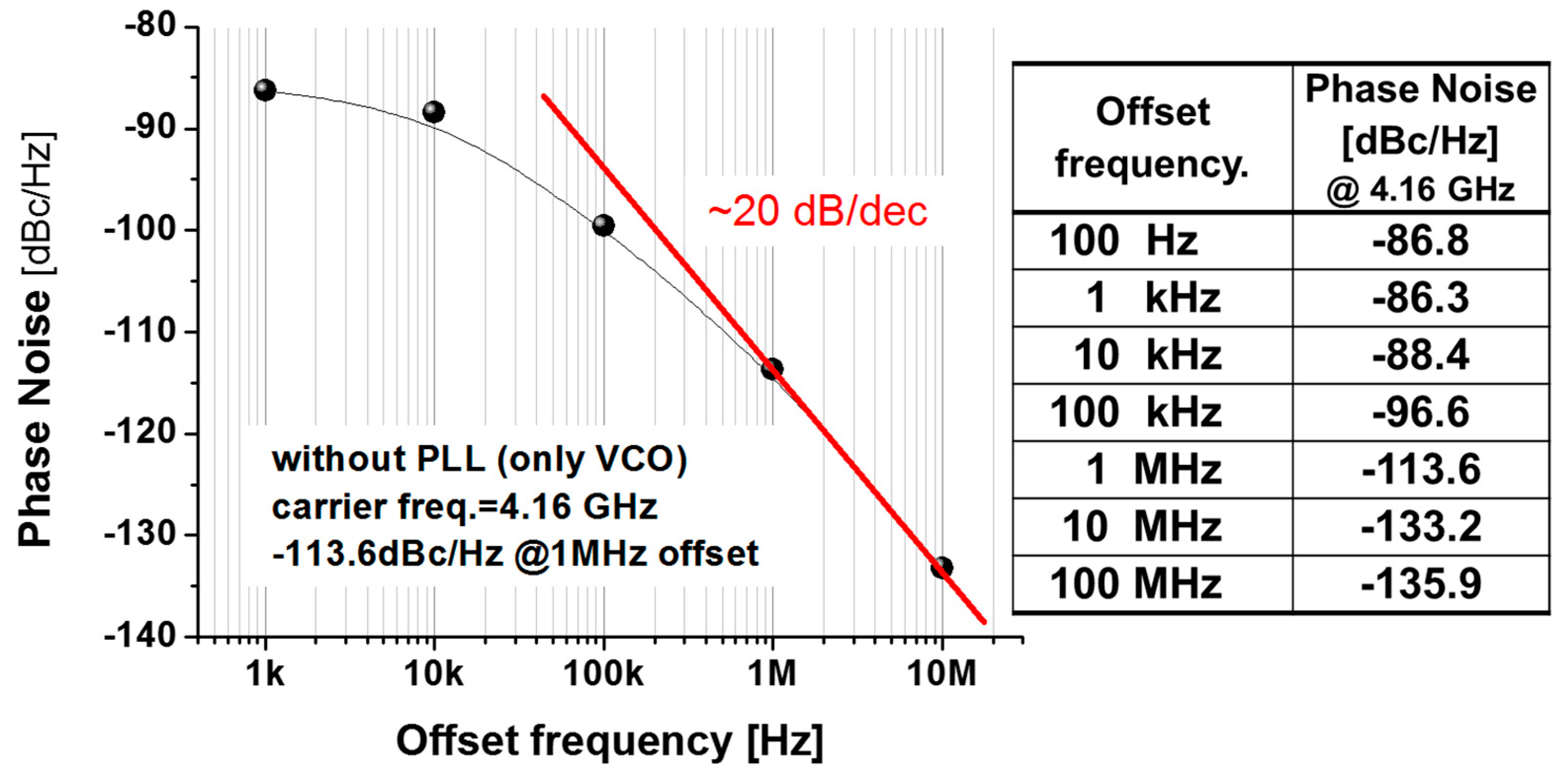
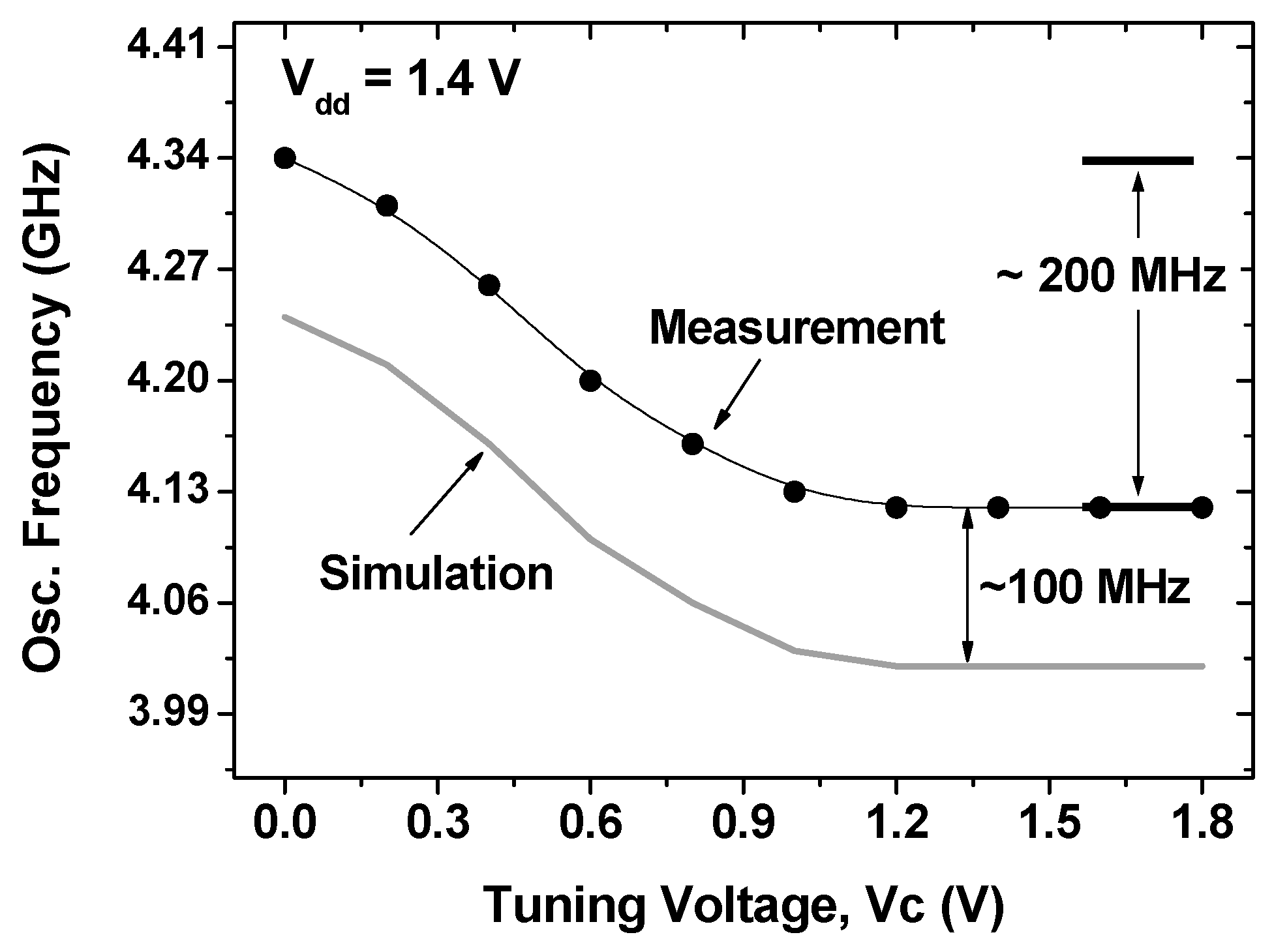
3. Experimental Results
4. Conclusions
Author Contributions
Funding
Conflicts of Interest
References
- Yao, Y.; Cao, Q.; Vasilakos, A.V. An energy-efficient, delay-aware, and lifetime-balancing data collection protocol for heterogeneous wireless sensor networks. IEEE/ACM Trans. Net. 2015, 23, 810–823. [Google Scholar] [CrossRef]
- Cattani, M.; Boano, C.A.; Römer, K. An Experimental Evaluation of the Reliability of LoRa Long-Range Low-Power Wireless Communication. J. Sens. Actuator Netw. 2017, 6, 7. [Google Scholar] [CrossRef]
- Viani, F.; Bertolli, M.; Salucci, M.; Polo, A. Low-Cost Wireless Monitoring and Decision Support for Water Saving in Agriculture. IEEE Sens. J. 2017, 17, 4299–4309. [Google Scholar] [CrossRef]
- Gil, J.; Song, S.-S.; Lee, H.; Shin, H. A −119.2 dBc/Hz at 1 MHz, 1.5 mW, fully integrated, 2.5-GHz, CMOS VCO using helical inductors. IEEE Microw. Wirel. Compon. Lett 2003, 13, 457–459. [Google Scholar]
- Lee, S.-H.; Chuang, Y.-H.; Chi, L.-R.; Jang, S.-L.; Lee, J.-F. A low-voltage 2.4GHz VCO with 3D helical inductors. IEEE APCCAS 2006, 518–521. [Google Scholar]
- Danesh, M.; Long, J.R. Differentially driven symmetric microstrip inductors. IEEE Trans. Microw Theory Tech. 2002, 50, 332–341. [Google Scholar] [CrossRef]
- Ooi, B.-L.; Xu, D.-X.; Kooi, P.-S. A comprehensive explanation on the high quality characteristics of symmetrical octagonal spiral inductor. Proc. IEEE Radio Freq. Integr. Circuits Symp. 2003, 259–262. [Google Scholar]
- Yue, C.P.; Wong, S.S. On-chip spiral inductors with patterned ground shields for Si-based RF IC’s. IEEE J. Solid-State Circuit 1998, 33, 743–752. [Google Scholar] [CrossRef]
- Hegazi, E.; Sjöland, H.; Abidi, A.A. A filtering technique to lower LC oscillator phase noise. IEEE J. Solid-State Circuits 2001, 36, 1921–1930. [Google Scholar] [CrossRef]
- Yu, S.-A.; Kinget, P.R. Scaling LC oscillators in nanometer CMOS technologies to a smaller area but with constant performance. IEEE Trans. Circuits Syst. II 2009, 56, 354–358. [Google Scholar]
- Moon, Y.-J.; Roh, Y.-S.; Jeong, C.-Y.; Yoo, C. A 4.39–5.26 GHz LC-Tank CMOS Voltage-Controlled Oscillator with Small VCO-Gain Variation. IEEE Microw. Wirel. Compon. Lett. 2009, 19, 524–526. [Google Scholar] [CrossRef]
- Park, D.; Cho, S.-H. H. A 1.8 V 900 μW 4.5 GHz VCO and Prescaler in 0.18 μm CMOS Using Charge-Recycling Technique. IEEE Microw. Wirel. Compon. Lett. 2009, 19, 104–106. [Google Scholar] [CrossRef]
- Lee, S.-H.; Chuang, Y.-H.; Jang, S.-L.; Chen, C.-C. Low-Phase Noise Hartley Differential CMOS Voltage Controlled Oscillator. IEEE Microw. Wirel. Compon. Lett. 2007, 17, 144–147. [Google Scholar] [CrossRef]
- Jerng, A.; Sodini, C.G. The impact of device type and sizing on phase noise mechanisms. IEEE J. Solid-State Circuits 2005, 40, 360–369. [Google Scholar] [CrossRef]
- Chu, Y.K.; Chuang, H.R. A fully integrated 5.8 GHz U-NII band 0.18-m CMOS VCO. IEEE Microw. Wirel. Compon. Lett. 2003, 13, 287–289. [Google Scholar]
- Tsai, M.-D.; Cho, Y.-H.; Wang, H. A 5-GHz low phase noise differential colpitts CMOS VCO. IEEE Microw. Wirel. Compon. Lett. 2005, 15, 327–329. [Google Scholar] [CrossRef]


| Ref. | Technology | fo (GHz) | Vdd (V) | Power Diss. (mW) | Phase Noise (dBc/Hz) | Offset Freq. (MHz) | Chip Size (mm2) | FoM (dB) | FoMA (dB) |
|---|---|---|---|---|---|---|---|---|---|
| This work | CMOS 0.18μm (MS) | 4.35 | 1.4 | 1.8 | −113.6 | 1.0 | 0.193 | 183.8 | 190.9 |
| [11] | CMOS 0.18μm (RF) | 5.20 | 1.8 | 9.7 | −113.7 | 1.0 | 0.350 | 180.0 | 184.6 |
| [12] | CMOS 0.18μm (RF) | 4.50 | 1.45 | 0.9 | −117.0 | 1.0 | 0.180 | 184.0 | 191.4 |
| [13] | CMOS 0.18μm (RF) | 4.50 | 1.5 | 6.8 | −122.5 | 1.0 | 0.546 | 187.0 | 189.6 |
| [14] | CMOS 0.18μm (RF) | 5.30 | 1.8 | 13.5 | −124.0 | 1.0 | − | 187.2 | − |
| [15] | CMOS 0.18μm (RF) | 5.80 | 1.8 | 8.1 | −110.0 | 1.0 | 0.806 | 176.2 | 177.1 |
| [16] | CMOS 0.18μm (RF) | 5.00 | 1.5 | 3.0 | −120.4 | 1.0 | 0.4125 | 189.6 | 193.4 |
© 2019 by the authors. Licensee MDPI, Basel, Switzerland. This article is an open access article distributed under the terms and conditions of the Creative Commons Attribution (CC BY) license (http://creativecommons.org/licenses/by/4.0/).
Share and Cite
Jhon, H.; Kim, M.-S.; Kang, M. Cost-Effective 4 GHz VCO Using Only Miniature Spirals Realized in a 0.18 μm CMOS Process for Wireless Sensor Network (WSN) Applications. Electronics 2019, 8, 1369. https://doi.org/10.3390/electronics8111369
Jhon H, Kim M-S, Kang M. Cost-Effective 4 GHz VCO Using Only Miniature Spirals Realized in a 0.18 μm CMOS Process for Wireless Sensor Network (WSN) Applications. Electronics. 2019; 8(11):1369. https://doi.org/10.3390/electronics8111369
Chicago/Turabian StyleJhon, Heesauk, Min-Su Kim, and Myounggon Kang. 2019. "Cost-Effective 4 GHz VCO Using Only Miniature Spirals Realized in a 0.18 μm CMOS Process for Wireless Sensor Network (WSN) Applications" Electronics 8, no. 11: 1369. https://doi.org/10.3390/electronics8111369