Article

An Inductive Isolation-Based 10 kV Modular Solid Boost-Marx Pulse Generator

State Key Laboratory of Power Transmission Equipment & System Security and New Technology, Chongqing University, Shapingba District, Chongqing 400044, China
*
Author to whom correspondence should be addressed.
Electronics 2023, 12(7), 1586; https://doi.org/10.3390/electronics12071586
Submission received: 26 February 2023 / Revised: 17 March 2023 / Accepted: 23 March 2023 / Published: 28 March 2023
(This article belongs to the Section Power Electronics)

Abstract

:
The solid-state Marx pulse generator is widely used in various fields such as biomedical electroporation, food processing, and plasma material modification. In this paper, an inductor is chosen as an isolation device and by adding a switch to the circuit, a solid-state boost-Marx pulse generator (BMPG) is formed. On the one hand, the inductor forms a boost circuit to multiply the output voltage gain, and on the other hand, it solves the shortcomings of conventional Marx pulse generators where the charging speed and total efficiency during high-frequency pulse generation are drastically affected by the isolation resistor. The selection criteria for inductors is well derived. Based on the PSpice simulation verification, a 12-module prototype of BMPG is built. The test results show that the circuit can achieve 10 kV high-voltage pulse output with a pulse width of 200–1000 ns and an adjustable repetition frequency of 0–10 kHz. While the input DC voltage requirement is only 235 V, the pulse voltage boost multiple is up to 42.5 times. Additionally, with the different switching sequences, the proposed BMPG can realize the adjustable change of pulse rising time and falling time.

1. Introduction

High-voltage nanosecond pulse generators are widely used in biomedical electroporation, high-energy electron accelerators, and plasma material modification applications [1,2,3,4,5]. Different amplitudes, pulse widths, and rise times of HV pulses have different effects in various applications. Compared to DC and AC power supply, power nanosecond pulses along the surface dielectric barrier discharge have high discharge efficiency, low gas temperature, uniform discharge, and other advantages [6].
In recent years, many scholars have researched plasma generation by nanosecond pulse [7,8,9]. The amplitude, width, frequency, and edge time of the high-voltage pulse power used need to be flexibly adjustable. Compared with magnetic pulse compression circuit [10,11], Blumlein [12,13], Linear Transformer Driver [14], and other pulse generation methods, the Marx circuit has a simple structure and flexible parameter adjustment [15,16,17,18]. Therefore, it is of great significance to design a portable high-frequency nanosecond Marx pulse generator with flexible and adjustable parameters for plasma jet research.
In [15,16], a traditional solid-state Marx pulse generation topology is proposed, which adopts a modular design to charge and discharge the energy storage capacitor. Each module consists of a switch, a capacitor, and two diodes.
To reduce the number of components and the need for DC charging voltage, a large number of papers have proposed new circuit structures. In [19], using the LC resonators is proposed to change the capacitor voltage’s polarity so that the same polarity in the series capacitor discharge and a high voltage pulse to obtain. Or adopt the diode commutation method to change the order of series connection of capacitors during discharge [20]. The above two circuit structures’ output pulse is not a square wave pulse with adjustable pulse rising time, and the value of the inductor changes with the pulse frequency.
In [21,22], a modular high-voltage pulse generator based on power electronic converters was proposed. A transformer is used in each module, which increases the pulse amplitude by increasing the number of modules and the transformer ratio. However, as the pulse voltage and frequency increase, the transformer’s magnetic leakage and saturation problems will affect the quality of the pulse waveform. In [23], a solid-state Marx generator based on a novel magnetic isolated drive is built and the maximum instantaneous power of this generator is 1.3 MW (30 kV, 43 A) with a pulse width of 3–10 μs and an adjustable repetition frequency of 0–1 kHz. Its disadvantage is that it uses 31 levels of sub-modules for stacking, which makes it difficult to achieve light weight and miniaturization due to its large size and low voltage gain.
In [24], the high module capacitances are charged by the former capacitors in series, which increases the output pulse amplification gain. Therefore, the above converters can generate high-voltage pulses by using a low-voltage source. However, as the number of stages increases, the voltage levels of energy storage capacitors and solid-state switches will increase dramatically. In [25], a 21-level prototype of the proposed inverter with 32 V input voltage and high gain 10 by using four modules was proposed. Each subsequent stage doubles the output voltage of the previous stage, resulting in a high step-up voltage gain. However, the implementation of the multilevel converter requires multiple levels of switch capacitor circuits, and the control strategy needs to be monitored and adjusted in real time, which makes the implementation relatively complex and increases system costs and difficulty.
In [26], a bipolar pulse source composed of two the boost converters for a mercury-free far UV-C (222 nm) excimer radiation source was proposed. The bipolar pulsed output voltage of up to 8 kV, having a pulse width of 1 µs and 5 µs, and a pulse repetition frequency of up to 50 kHz is achieved. However, the system can be expensive to manufacture and maintain and the equipment is bulky and difficult to carry. In [27], a pulse generator using a buck-boost converter was proposed, but an HV solid-state switch is required in the output stage to control the output of HV pulses directly. In [28], a boosted bipolar pulse generator was realized by turning on and off multiple sets of switches. In [29], an inductive energy storage solid-state Marx circuit was proposed, whose output pulse amplitude can reach multiple times that of a conventional solid-state Marx circuit. However, inductance devices need to be added to each module. Only the spike in the rising edge of the pulse has an increase in amplitude, but the flat top of the output pulse does not increase. In [30], a multiple toroidal transformers-based ringing circuit for a unipolar high-voltage pulse generator is proposed. However, this design requires the use of a large number of capacitors and spark gaps, taking up a lot of space and adding cost and complexity.
In order to output high-voltage pulses, the Marx circuit usually requires a high-voltage DC power supply to charge the capacitor. In the case of ensuring that the pulse waveform is a square wave, it is often impossible to reduce the number of devices in the circuit and increase the voltage gain at the same time. This paper proposes a boosted Marx pulse generator, whose amplitude and pulse width are flexibly adjustable, and can be widely used in electroporation and plasma material modification applications. Compared with the simple circuit in [15,16], the proposed circuit topology only adds a switch with the same voltage level as other modules, as shown in Figure 1. By adjusting the inductor charging time to change the gain multiple of the pulse amplitude, the requirement for the input DC voltage source is reduced, and the number of circuit modules is reduced. In addition, all solid-state switches in the topology are at the same voltage level, which is more conducive to the stable operation and expansion of the entire system.
The mathematical analysis and circuit component design of the proposed circuit is introduced in detail. The theoretical feasibility is verified by PSPice simulation software. Finally, the pulse generator is evaluated by building and simulating the actual circuit of the parameter 1:1. It is proved that when the charging voltage is DC 235 V, a high voltage pulse of 10 kV can be obtained.

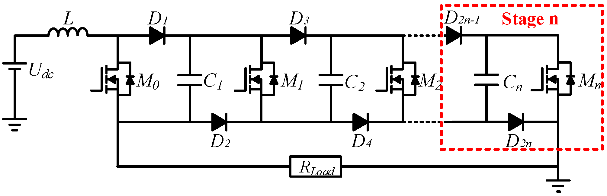
2. Topology and Operation Principle of Proposed Boost-Marx Pulse Generator
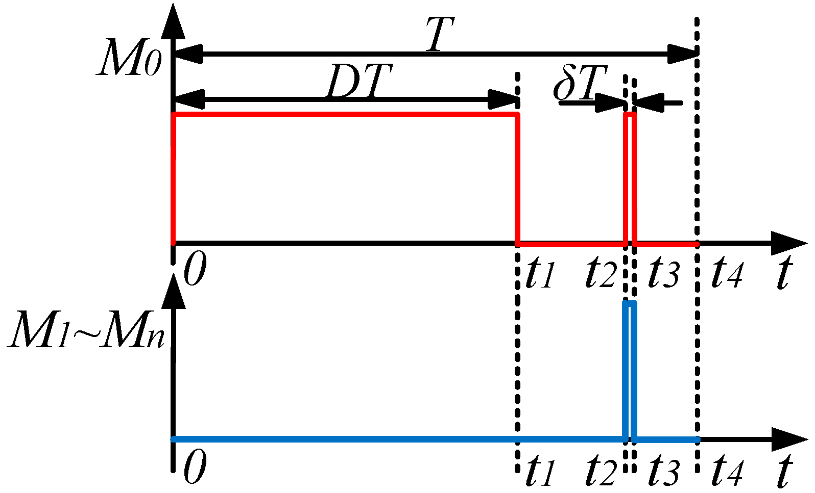
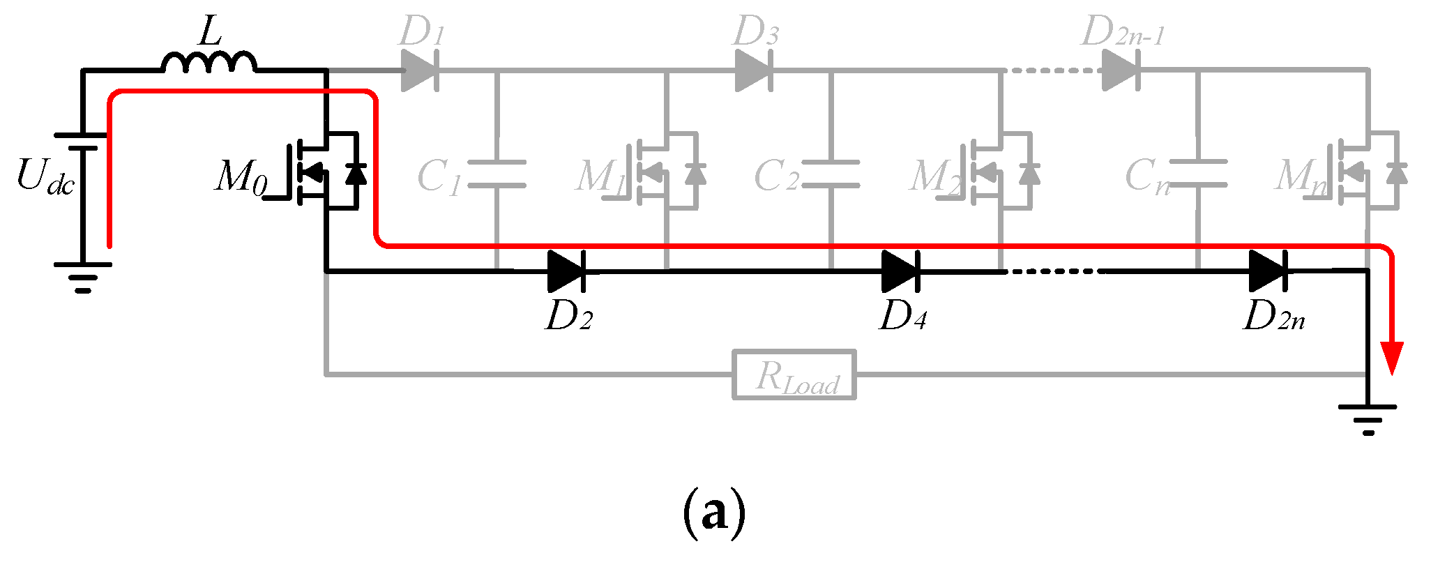
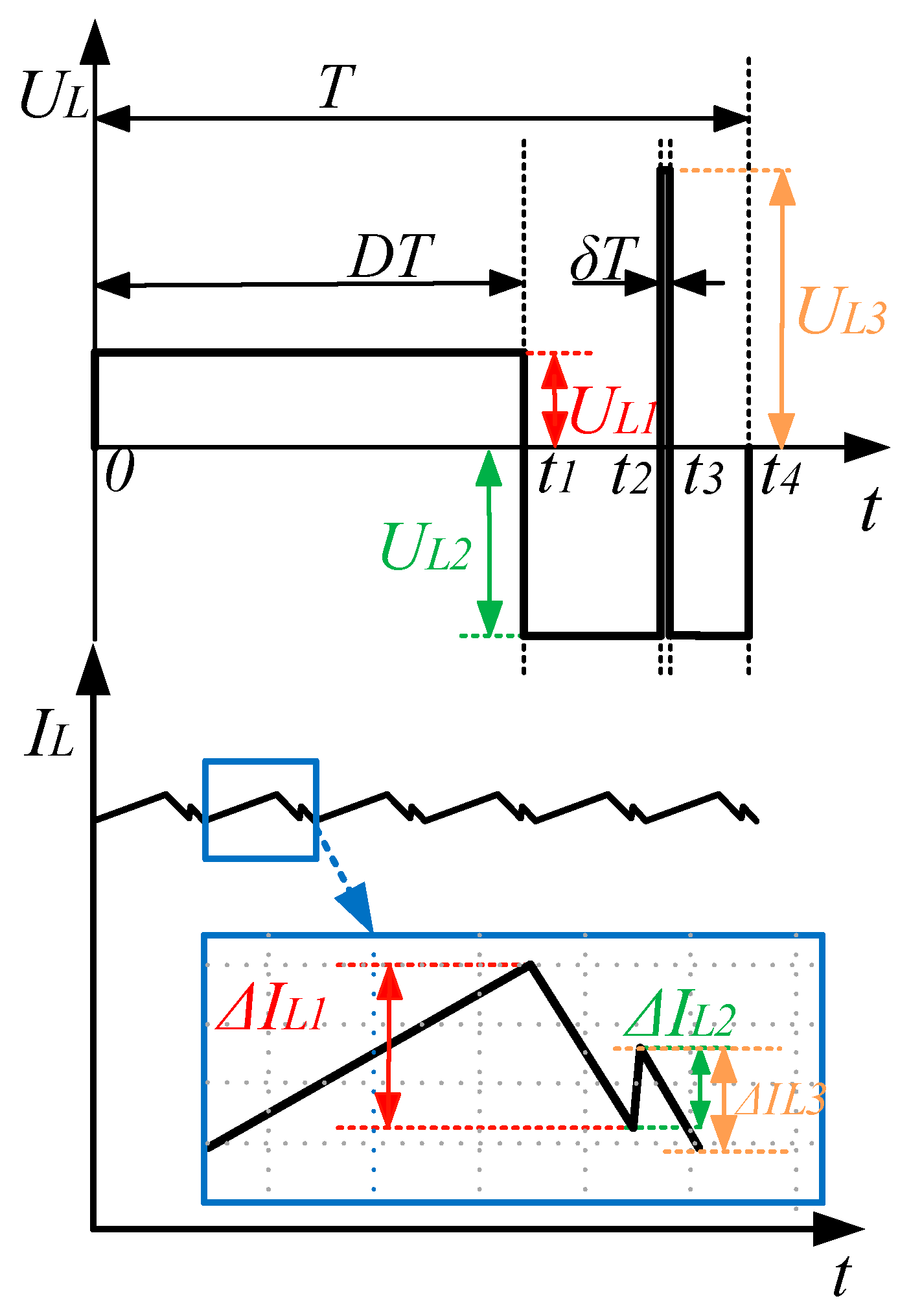
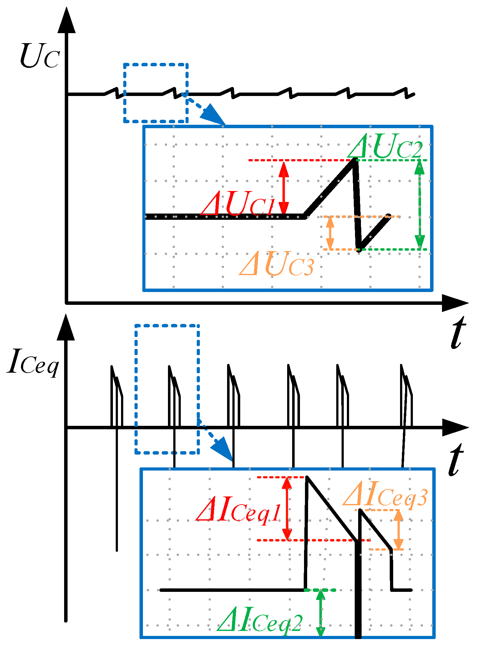
The basic circuit topology of the Boost-Marx pulse generator is shown in Figure 1. Figure 2 illustrates the on-off timing sequence of MOSFET in the circuit propose. According to the different operating modes of the circuit, a switching cycle Ts can be divided into four modes, wherein DT is the on-time of M0 and δT is the discharge time of the pulse circuit when M0~Mn is on. It is assumed that all semiconductor devices such as MOSFETs and diodes in the BMPG are ideal components. When they are turned on, the voltage between them is zero. The four operating modes in one cycle can be explained as follows:

2.1. Mode 1 [0, t1]

BMPG works in inductor charging mode, as shown in Figure 3a. The switch M0 in the circuit is turned on, and switches M1~Mn are turned off. The duration of this mode is DT. The DC power supply Udc charges the inductor L through M0, D2, D4D2n. At this time, the inductor voltage is equal to the input DC power supply voltage, and the charging current can be expressed by Equation (1):
d i L d t = U L L = U d c L

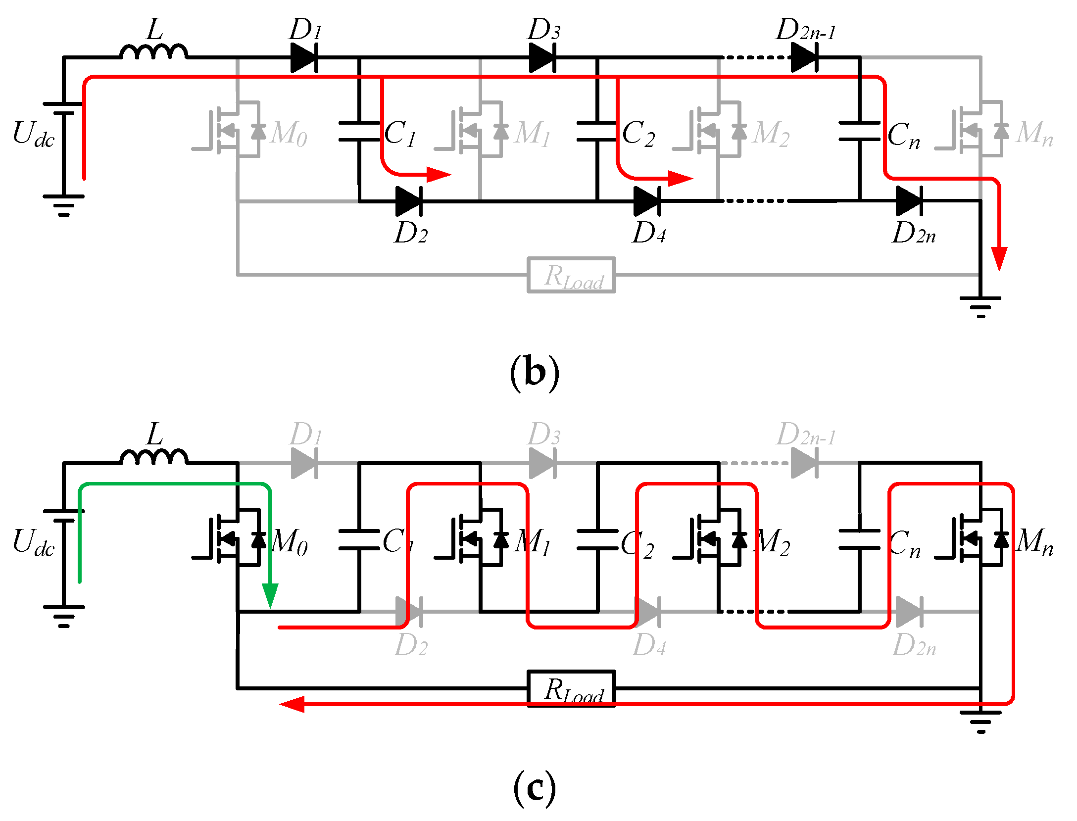
2.2. Mode 2 [t1, t2]

BMPG works in capacitor charging mode, as shown in Figure 3b. All switches in the circuit are turned off, and the DC power supply Udc and the inductor L charge the capacitors C1~Cn through the diodes D1~Dn. The charging equivalent circuit diagram is shown in Figure 4. All the capacitors in the circuit are connected in parallel, the value of the equivalent capacitor Ceq is equal to the sum of all the energy storage capacitors, and its value is nC. The voltage value of the equivalent capacitor Ueq is equal to the voltage of each capacitor. The equivalent current Ieq is the sum of each branch. Consequently, the expressions of the voltage and current of equivalent capacitor can be represented as:
U e q = U d c + U L
i C = i L = C d u C d t
When the pulse power supply works at a higher pulse repetition frequency, a larger inductor is required to make it run in the CCM mode, so the energy storage capacitor is always charged in this mode until the pulse trigger signal arrives.

2.3. Mode 3 [t2, t3]

When the pulse trigger signal arrives, BMPG works in pulse discharge mode, as shown in Figure 3c. All the switches in the circuit are turned on, and C1~Cn are discharged in series through the switches M1~Mn. At this time, the equivalent capacitance discharged in series is C/n. The output pulse voltage is estimated as (4). There is a short-term high voltage on the inductor, which can be calculated by Equation (5).
U o u t = n U C
U L = n U C + U d c

2.4. Mode 4 [t3, t4]

After the pulse discharge is completed, all the switches are closed at the same time. Like Mode 2, the DC power supply and the inductor charge the capacitor in parallel, as shown in Figure 3b. The capacitor voltage can be represented by (6). The end of this process means the completion of the entire cycle.
U C = 1 C t 3 t 4 i C d t
In one working cycle, the current through the equivalent capacitor in the capacitor charging mode is equal to the sum of the current through C1~Cn. In a working cycle, in the charging state, the current flowing through the equivalent capacitor is equal to the sum of the current flowing through C1~Cn. In the capacitor pulse discharge mode, the equivalent capacitor’s total current is equal to the current of each capacitor branch, as shown in Figure 5 and Figure 6. There are two processes of capacitor charging. The charging voltages are represented by (7) and (9), respectively. The discharge mode can be equivalent to discharging the capacitor to the load. The capacitor voltage drop caused by this process can be represented by Formula (8). The three reach equilibrium in one cycle. Under normal circumstances, the pulse voltage can reach several kV, which is much larger than the voltage in the balanced state of the capacitor. The current, that is, the current value of the pulse output, can be approximated as (11).
U C e q 1 = 1 C e q t 1 t 2 I L d t
U C e q 2 = 1 C e q t 2 t 3 I C e q d t = U C ( 1 e n δ T R C )
U C e q 3 = 1 C e q t 3 t 4 U C U d c L d t
U C e q 2 = U C e q 1 + U C e q 3
I o u t = I C e q = U o u t R = n U C R
As an important energy storage element in the circuit, the voltage of the inductor in one cycle is shown in Figure 5. According to the volt-second balance principle, the expression can be obtained as:
0 T u L d t = 0
U L 1 D T + U L 3 δ T = U L 2 ( T D T δ T )
Substituting Formulas (2), (5), and (6) into the above formula, the voltage gain β is:
β = U 0 U d c = n 1 D ( n + 1 ) δ

3. Parameter Selection and Comparative Analysis

Devices such as isolating charging inductors, energy storage capacitors, and switches directly affect the circuit’s working conditions. Therefore, this section will derive the selection criteria for inductors and capacitors based on the working principle of BMPG.

3.1. Parameter Selection

In the solid-state Marx circuit, a resistor or inductor needs to be connected at the input to solve the problem of high-voltage isolation between the DC power supply and the discharge circuit. At the moment of discharge, the inductor can limit the magnitude of the DC power supply current, which is represented by Formula (15).
1 L 0 δ T ( U d c + n U C ) d t < I n o m
In the topology proposed in this paper, the inductor not only achieves isolation, but also acts as an energy storage element in the circuit. By changing the time of charging and discharging, the amplitude of the output pulse can be controlled. In order to make the pulse generator frequency reach the kHz level, a larger inductor is used to make it work in CCM mode, which meets the Formula (9). When the pulse generator reaches a steady state, the inductor balances charge and discharge within a period T.
Define η to be the efficiency of the entire circuit. In a cycle, the energy consumed by the load can be expressed by Equation (16). The average value of the input current is obtained from the conservation of energy.
E o u t = 0 δ T I 0 × U 0 d t ( β U d c ) 2 R δ T
E i n = U d c I i n T
I i n = β 2 δ U d c η R
As shown in Figure 5, when the current is lower than the average current, the maximum inductor current ripple appears before the pulse discharge, and its value can be calculated as:
I L 1 = U d c D T L
I L 2 < ( U C U d c ) ( 1 D δ ) T L
I m a x < ( n + 1 ) ( 1 δ ) D 1 D ( n + 1 ) δ × U d c δ T L
In order for the inductor current to be continuous, the average value of the current must be greater than the maximum ripple current. The value of the inductor can be derived as:
L > n β 1 R β 2 f
In order to ensure that the output pulse is a rectangular wave and satisfy that the voltage on the capacitor is higher than a certain minimum voltage value required, while the Marx circuit is discharging under the maximum pulse width, the voltage drop is ∆Ud. the value of the required capacitor can be calculated as:
C s e r i e s > C n δ T × U 0 U d × R

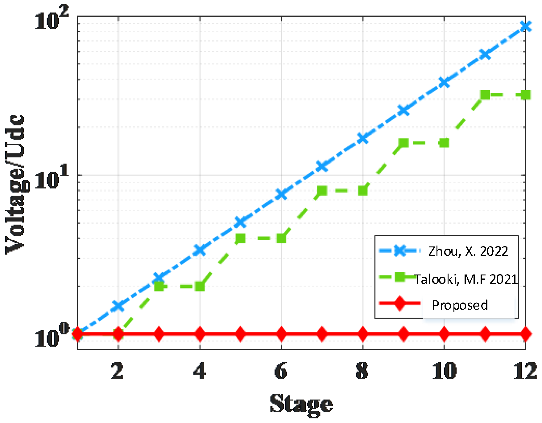
3.2. Comparative Analysis

After device parameter calculation and quantity selection, this article proceeded to analyze and compare the results with six other similar topologies. Table 1 shows the number of devices included in the circuit and the pulse voltage gain, where n is the number of modules in the circuit.
As a conventional solid-state Marx, the structure in [15,16,17] is simple, and the number of components is small. However, the pulse voltage gain is only equal to the number of modules in the circuit. In [21], each module needs to use an inductor to increase the single-stage output voltage. After voltage transformation and boosting, the output of high-voltage pulses is realized through the output control module, where m is the number of bridge arm control modules, and N is the transformer ratio. The introduction of these inductors and transformers not only causes the complexity of the circuit and increases the cost but also causes the pulse waveform to be distorted, which is not a rectangular pulse wave. In [27], an inductor is used for charging and boosting, but a high-voltage switch is also required to cut off the high voltage at the output. Therefore, in high-voltage applications, the use of high-voltage devices such as thyristors is inevitable.
In [23], each stage of its capacitor is charged by the upper stage of the boost circuit. If the discharge time is long, the voltage level of each level module increases exponentially. However, if the pulse discharge time is short, the boosting effect is not obvious. In [25], the pre-stage capacitor is used to charge the pressure, and the output voltage of the pulse is increased when the series is connected. However, this step-up method will continuously increase the voltage level of the subsequent modules.
On the basis of the basic solid-state Marx circuit, the circuit proposed in this paper can realize the output of several times the pulse voltage by just adding a switch. Figure 7 shows the comparison of the voltage levels of each module in the case of 12 modules in [23,25], and the topology proposed in this paper. When the DC charging voltage of the three circuits is Udc, the voltage of each module of the circuit proposed in this paper remains unchanged, which is Udc. In order to make the output voltage of [23] have a significant gain, suppose it works under the working condition of longer charging time, and the boost multiple between each level is assumed to be 1.5. Through the comparison, it can be found that, with the continuous improvement of voltage levels in [23,25], the voltage level of each module in the topology proposed in this paper is the same, which reduces the requirements for the voltage level of the device and is more conducive to modular expansion.

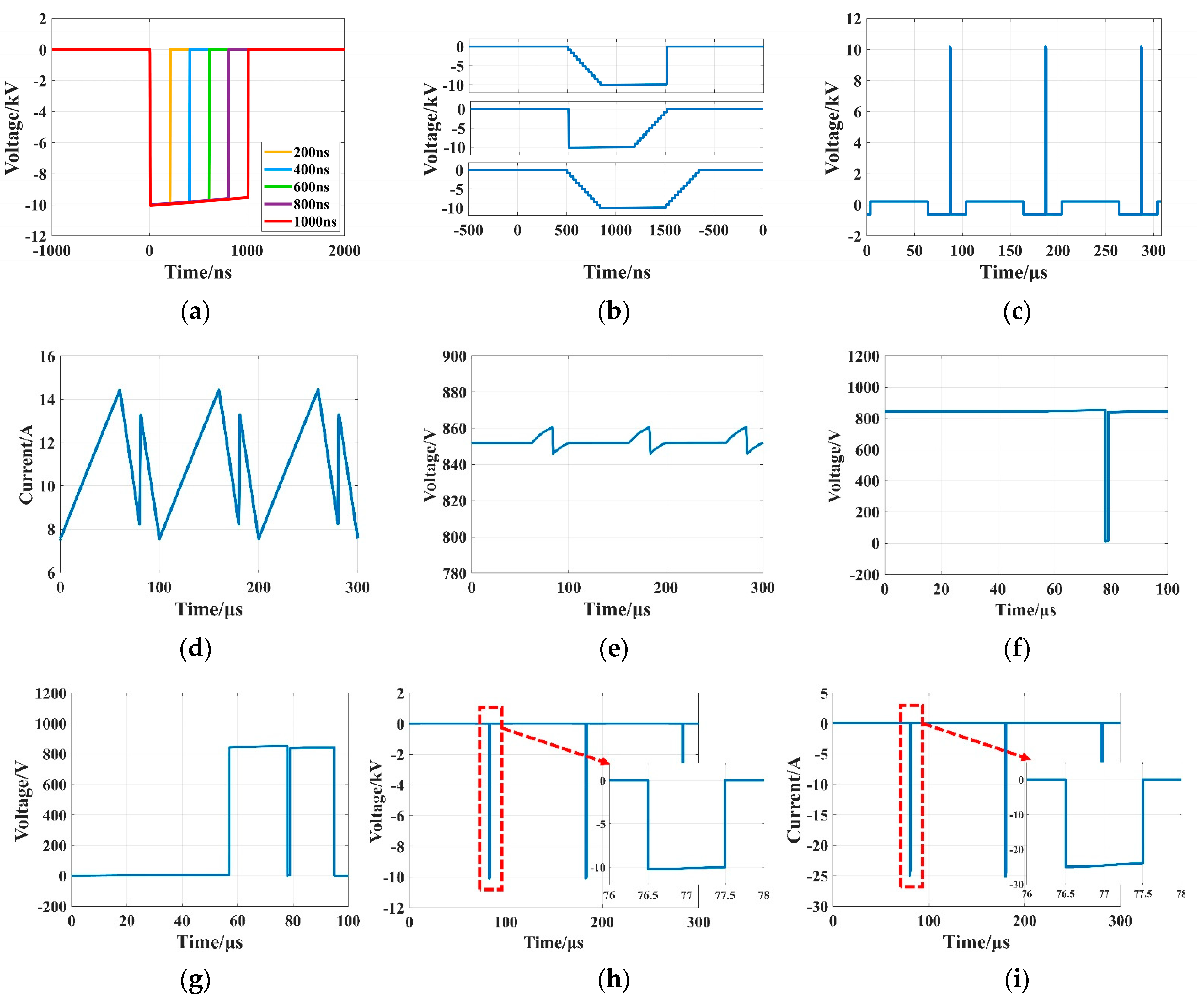
4. Simulation Results

In order to verify the theoretical feasibility of the BMPG proposed in this paper, PSpice software is used for simulation verification and the simulation parameters are shown in Table 2. The HBPG consists of 12-stage modules on which the different parameters of the output pulse are compared.
Figure 8 shows the different pulse parameters used in plasma discharge research. The voltage waveform under different pulse widths is shown in Figure 8a, and its range is 200–1000 ns. Because voltage gain is related to δ, as δ increases, the output voltage will decrease slightly. By adjusting the input voltage or the duty cycle D, different pulse widths can be achieved when the output pulse is 10 kV. Figure 8b shows the changes in the rise and fall times of the pulses generated when the switches M1M12 are adjusted in different switching sequences. The delay time between each switch is 30 ns, which realizes the adjustable change of pulse rising time, falling time, or the above two.
The voltage and current waveforms of the key devices in the BMPG are shown in Figure 8c–g. Among them, Figure 8c is the voltage waveform at both ends of the inductor, Figure 8d is the current waveform flowing through the inductor, and the inductor is in a charge-discharge balance state within one cycle. The voltage of the energy storage capacitor is shown in Figure 8e. In addition, Figure 8g,f, respectively, show the voltage levels of the switch M0 and the discharge switches M1~M12 in each mode, proving that their voltage levels are the same.

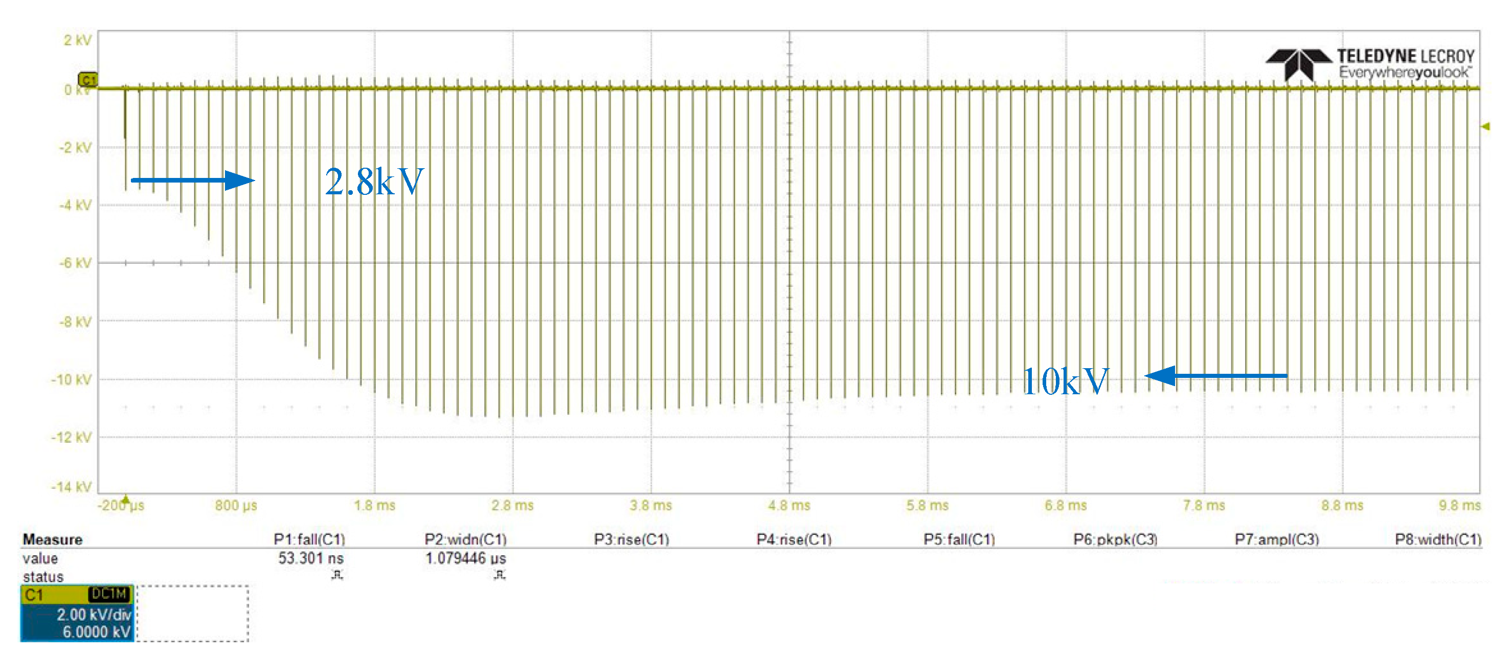
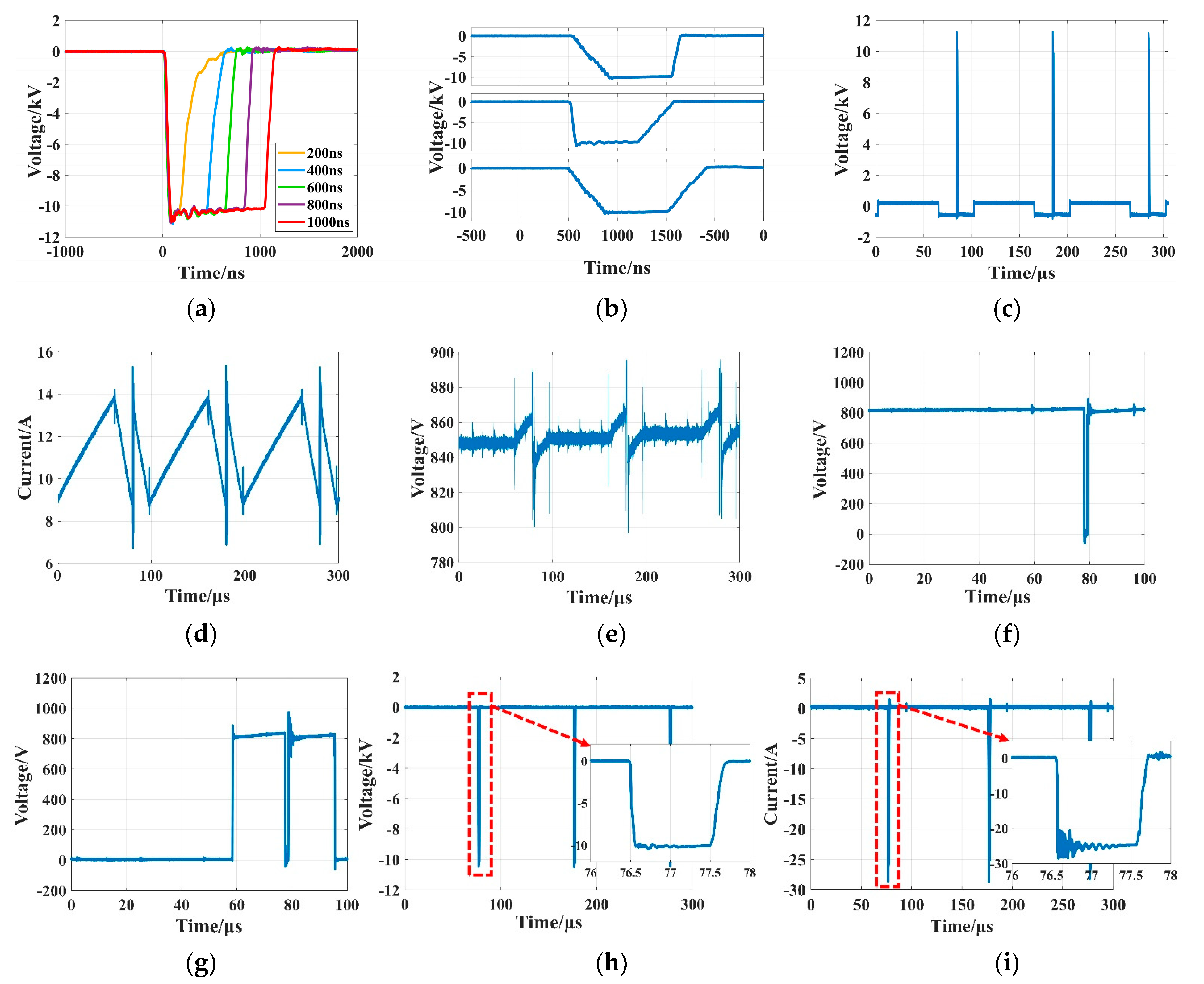
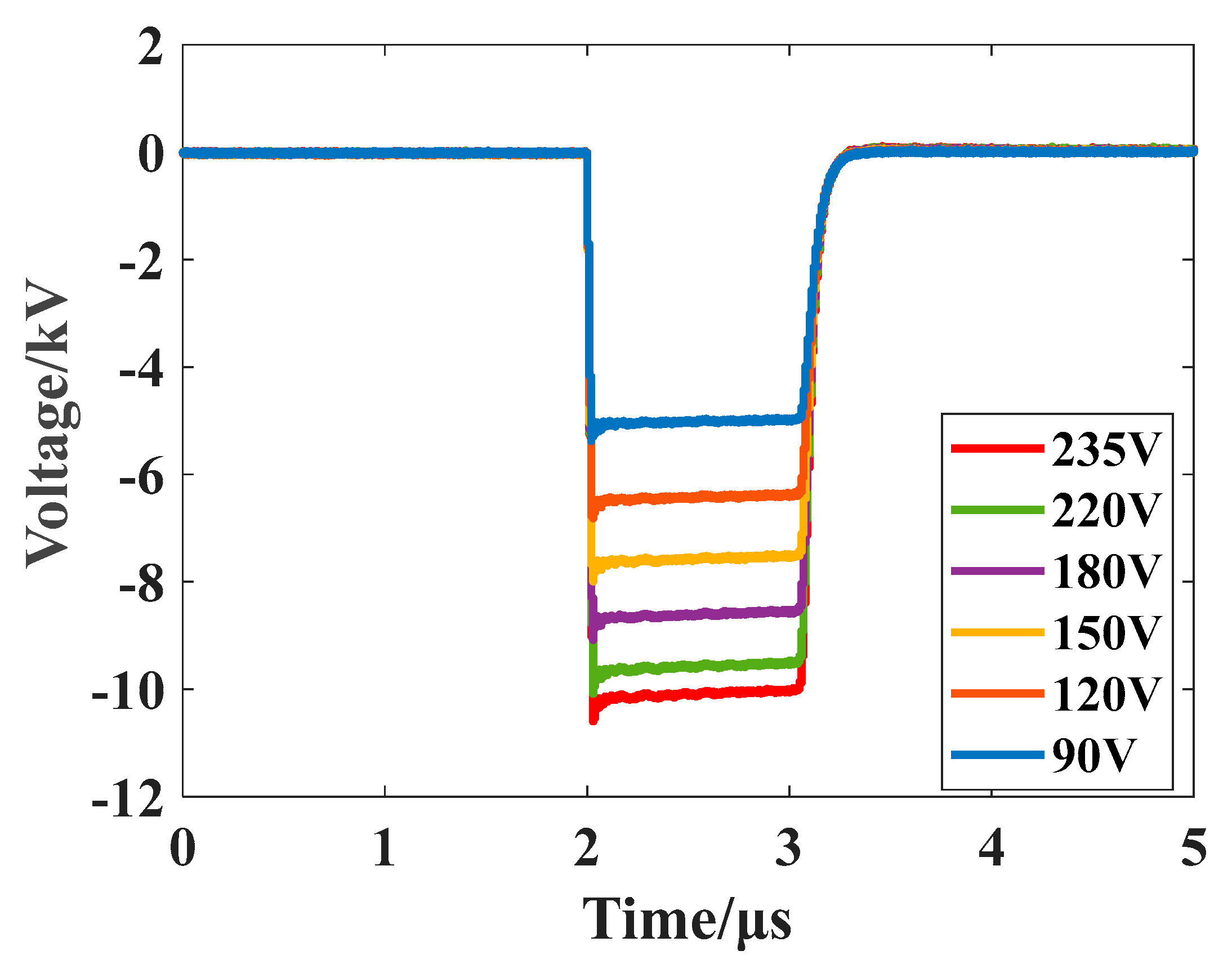
5. Experimental Results

To demonstrate the functionality of the BMPG and to confirm the validity of the mathematical analyses and simulation results, a hardware prototype was designed with the parameters listed in Table 3. The experimental setup is depicted in Figure 9. Under the condition that the duty cycle D is equal to 0.61 for a certain period of time, the amplitude of different output pulses is obtained by increasing the input voltage from 90 to 235 V, as shown in Figure 10. By changing the switch discharge time, the output pulse width is adjusted. The pulse width ranges from 200 ns to 1000 ns, as shown in Figure 11a. The trigger delay time of 12 discharge switches is controlled by FPGA to realize the change of falling time and rising time of the output pulse. The discharge delay time of each stage is 30 ns, and the falling or rising time of the changed output pulse is increased to about 400 ns. Compared with isolated resistive, when an inductance device is used at the input, the charging speed of the energy storage capacitor is faster and the loss is smaller, so it can work continuously at high frequency. In the experiment of this paper, the pulse frequency is running at 10 kHz.
Figure 11c–e shows the voltage and current waveforms on the inductor when the output is stable. Figure 11f,g show the voltages on the gates and drains of the switches M0~M12. Experiments have proved that, including the switch M0 used for chopping, all switches have the same voltage level. This also shows that adding a chopper switch will not increase the voltage level of the Marx circuit switching device, which will be conducive to the expansion of topology modularity. Figure 11h,i are the voltage and current waveforms of the output pulse. Experiments show that BMPG can still ensure that the output pulse is a rectangular wave. The above experimental results are also in good agreement with the simulation results in the previous section. During the initial time of pulse output, the pulse voltage amplitude is a growing process, and the voltage amplitude increases from nUdc to βnUdc, as shown in Figure 12.

6. Conclusions

In this paper, a high-gain pulse generator topology is proposed that is suitable for plasma jet applications. The proposed topology utilizes an inductor as the isolation device for the solid-state Marx circuit. With the addition of only one switch, the inductor is used to charge and discharge, resulting in a high gain of output pulse amplitude. Unlike traditional Marx circuits, the proposed BMPG circuit does not use any inductors or magnetic core devices such as transformers, ensuring that the output pulse is always a square wave pulse. Additionally, the voltage levels of modules are consistent and do not increase with the number of modules, allowing for easy expansion. The BMPG circuit provides economic and reliable advantages while improving gain ratio and adjustment flexibility. As a result, complex topologies such as bipolar and truncated circuits can be implemented with lower DC input voltage or fewer circuit modules. The main contributions of the BMPG proposed in this paper can be summarized as follows:
(1)
This article uses an inductive isolator on the basis of the traditional Marx circuit, and with the addition of only one solid-state switch to increase the gain of the output voltage pulse.
(2)
BMPG completes the isolation between the pulse generator and the DC power supply, reducing the voltage amplitude requirements of the DC power supply, and the entire system is modular and scalable.
(3)
The amplitude of the output pulse can be adjusted by varying the duty cycle D, and a new control method is proposed to make the adjustment more flexible. This provides a basis for the closed-loop control of the pulse power supply in the future.

Author Contributions

Conceptualization, Y.J. and L.C.; methodology, Y.J.; software, Y.J.; validation, Y.J.; formal analysis, Y.J.; investigation, Y.J.; resources, Y.J.; data curation, Y.J.; writing—original draft preparation, Y.J.; writing—review and editing, L.C.; visualization, L.C.; supervision, L.C.; project administration, L.C.; funding acquisition, L.C. All authors have read and agreed to the published version of the manuscript.

Funding

This research received no external funding.

Data Availability Statement

Data sources used are described in the article. Simulation results will be made available in Pspice by March 2023.

Acknowledgments

This research was supported by Yu Liang, Yao Chenguo and Dong Shoulong of Chongqing University. We would like to give thanks to their support and guidance.

Conflicts of Interest

The authors declare no conflict of interest.

References

  1. Lv, Y.; Yao, C.; Rubinsky, B. A 2-D Cell Layer Study on Synergistic Combinations of High-Voltage and Low-Voltage Irreversible Electroporation Pulses. IEEE Trans. Biomed. Eng. 2020, 67, 957–965. [Google Scholar] [CrossRef]
  2. Zeng, W.; Yu, L.; Dong, S.; Ma, J.; Wang, Y.; He, Y.; Wang, X.; Yao, C. A Novel High-Frequency Bipolar Pulsed Power Generator for Biological Applications. IEEE Trans. Power Electron. 2020, 35, 12861–12870. [Google Scholar] [CrossRef]
  3. Petr, R.; Reilly, D.; Freshman, J.; Orozco, N.; Pham, D.; Ngo, L.; Mangano, J. Solid-state pulsed power for driving a high-power dense plasma focus x-ray source. Rev. Sci. Instrum. 2000, 71, 1360–1362. [Google Scholar] [CrossRef]
  4. Yamamoto, A.; Kawano, Y.; Nakai, M.; Nakagawa, T.; Sakugawa, T.; Hosseini, H.; Akiyama, H. Investigation of gas flow dependence of plasma jet produced by pulsed power. IEEE Trans. Plasma Sci. 2015, 43, 3451–3455. [Google Scholar] [CrossRef]
  5. Elserougi, A.A.; Faiter, M.; Massoud, A.M.; Ahmed, S. A Transformerless Bipolar/Unipolar High-Voltage Pulse Generator With Low-Voltage Components for Water Treatment Applications. IEEE Trans. Ind. Appl. 2017, 53, 2307–2319. [Google Scholar] [CrossRef]
  6. Zhang, S.; Wang, W.C.; Jiang, P.C.; Yang, D.Z.; Jia, L.; Wang, S. Comparison of atmospheric air plasmas excited by high-voltage nanosecond pulsed discharge and sinusoidal alternating current discharge. J. Appl. Phys. 2013, 114, 163301. [Google Scholar] [CrossRef]
  7. Jiang, J.; Shao, S.; Zhang, C.; Li, W.; Yan, P.; Che, X.; Schamiloglu, E. Experimental study of Q-V Lissajous figures in nanosecond-pulse surface discharges. IEEE Trans. Dielectr. Electr. Insul. 2013, 20, 1101–1111. [Google Scholar] [CrossRef]
  8. Xie, Q.; Gan, W.; Zhang, C.; Che, X.; Yan, P.; Shao, T. Effect of rise time on nanosecond pulsed surface dielectric barrier discharge actuator. IEEE Trans. Dielectr. Electr. Insul. 2019, 26, 346–352. [Google Scholar] [CrossRef]
  9. Benard, N.; Zouzou, N.; Claverie, A.; Sotton, J.; Moreau, E. Optical visualization and electrical characterization of fast-rising pulsed dielectric barrier discharge for airflow control applications. J. Appl. Phys. 2012, 111, 033303. [Google Scholar] [CrossRef]
  10. Tao, Y.; Li, S.; Li, Q.; Tian, Y.; Wang, Z.; Cheng, F. Study on the influence of core material on the performance of nanosecond pulse power supply. In Proceedings of the 2017 1st International Conference on Electrical Materials and Power Equipment (ICEMPE), Xi’an, China, 14–17 May 2017; pp. 122–127. [Google Scholar]
  11. Li, S.; Gao, J.; Yang, H.; Zhu, D.; Qian, B.; Cui, Y.; Han-Wu, Y.; Zhang, J. Investigation on Adjustable Magnetic Pulse Compressor in Power Supply System. IEEE Trans. Power Electron. 2019, 34, 1540–1547. [Google Scholar] [CrossRef]
  12. Yu, L.; Jiu, Z.; Sugai, T.; Tokuchi, A.; Jiang, W. Pulsed Voltage Adder Topology Based on Inductive Blumlein Lines. IEEE Trans. Plasma Sci. 2018, 46, 1816–1820. [Google Scholar] [CrossRef]
  13. He, Y.; Ma, J.; Yu, L.; Dong, S.; Gao, L.; Zeng, W.; Yao, C. 10-MHz High-Power Pulse Generator on Boost Module. IEEE Trans. Ind. Electron. 2020, 68, 6286–6296. [Google Scholar] [CrossRef]
  14. Kazemi, M.R.; Sugai, T.; Tokuchi, A.; Jiang, W. Waveform Control of Pulsed-Power Generator Based on Solid-State LTD. IEEE Trans. Plasma Sci. 2016, 45, 247–251. [Google Scholar] [CrossRef]
  15. Redondo, L.; Silva, J.; Tavares, P.; Margato, E. High-voltage high-frequency Marx-bank type pulse generator using integrated power semiconductor half-bridges. In Proceedings of the 2005 European Conference on Power Electronics and Applications, Dresden, Germany, 11–14 September 2005; p. 8. [Google Scholar]
  16. Yao, C.; Zhang, X.; Guo, F.; Dong, S.; Mi, Y.; Sun, C. FPGA-Controlled All-Solid-State Nanosecond Pulse Generator for Biological Applications. IEEE Trans. Plasma Sci. 2012, 40, 2366–2372. [Google Scholar] [CrossRef]
  17. Zeng, W.; Yao, C.; Dong, S.; Wang, Y.; Ma, J.; He, Y.; Yu, L. Self-Triggering High-Frequency Nanosecond Pulse Generator. IEEE Trans. Power Electron. 2020, 35, 8002–8012. [Google Scholar] [CrossRef]
  18. Shi, H.; Lu, Y.; Gu, T.; Qiu, J.; Liu, K. High-voltage pulse waveform modulator based on solid-state Marx generator. IEEE Trans. Dielectr. Electr. Insul. 2015, 22, 1983–1990. [Google Scholar] [CrossRef]
  19. Zabihi, S.; Zare, F.; Ledwich, G.; Ghosh, A.; Akiyama, H. A new family of marx generators based on commutation circuits. IEEE Trans. Dielectr. Electr. Insul. 2011, 18, 1181–1188. [Google Scholar] [CrossRef] [Green Version]
  20. Zabihi, S.; Zabihi, Z.; Zare, F. A Solid-State Marx Generator With a Novel Configuration. IEEE Trans. Plasma Sci. 2011, 39, 1721–1728. [Google Scholar] [CrossRef] [Green Version]
  21. Darwish, A.; Elgenedy, M.A.A.; Finney, S.J.; Williams, B.W.; McDonald, J.R. A Step-Up Modular High-Voltage Pulse Generator Based on Isolated Input-Parallel/Output-Series Voltage-Boosting Modules and Modular Multilevel Submodules. IEEE Trans. Ind. Electron. 2017, 66, 2207–2216. [Google Scholar] [CrossRef] [Green Version]
  22. Banaei, R.; Khiz, A. New modular high-voltage pulse generator based on SEPIC converter for electroporation applications. IET Power Electron. 2020, 13, 3072–3080. [Google Scholar] [CrossRef]
  23. Zhou, X.; Zhang, Z.; Dong, S.; Yu, L.; Liu, J.; Qiao, X.; Yao, C. High Voltage Pulse Generator Based on a Novel Magnetic Isolated Drive Circuit. IEEE Trans. Power Electron. 2022, 37, 8157–8166. [Google Scholar] [CrossRef]
  24. Khosravi, R.; Rezanejad, M. A New Pulse Generator With High Voltage Gain and Reduced Components. IEEE Trans. Ind. Electron. 2019, 66, 2795–2802. [Google Scholar] [CrossRef]
  25. Talooki, M.F.; Rezanejad, M.; Khosravi, R.; Samadaei, E. A Novel High Step-Up Switched-Capacitor Multilevel Inverter With Self-Voltage Balancing. IEEE Trans. Power Electron. 2021, 36, 4352–4359. [Google Scholar] [CrossRef]
  26. Ram, S.K.; Devassy, S.; Lakshmanan, P.; Mishra, S. High-Voltage Bipolar Pulsed Power Supply for Mercury-free Far UV-C Excimer Radiation Source. In Proceedings of the 2022 IEEE 10th Power India International Conference (PIICON), New Delhi, India, 25–27 November 2022; pp. 1–5. [Google Scholar] [CrossRef]
  27. Taherian, M.; Allahbakhshi, M.; Farjah, E.; Givi, H. A Modular Topology of Marx Generator Using Buck–Boost Converter. IEEE Trans. Plasma Sci. 2019, 47, 549–558. [Google Scholar] [CrossRef]
  28. Malviya, D.; Veerachary, M. A Boost Converter-Based High-Voltage Pulsed-Power Supply. IEEE Trans. Ind. Appl. 2020, 56, 5222–5233. [Google Scholar] [CrossRef]
  29. Ren, X.; Sugai, T.; Tokuchi, A.; Jiang, W. Solid-State Marx Generator Circuit With Inductive Booster. IEEE Trans. Plasma Sci. 2020, 49, 378–382. [Google Scholar] [CrossRef]
  30. Abdel-Azim, W.E.; Elserougi, A.A.; Hossam-Eldin, A.A. A Voltage-Doubler/Marx-Generator-Based Multi-Module High-Voltage Pulse Generator with High-Frequency Charger for Electrostatic Precipitators. In Proceedings of the 2022 23rd International Mid-dle East Power Systems Conference (MEPCON), Cairo, Egypt, 13–15 December 2022; pp. 1–7. [Google Scholar] [CrossRef]
Figure 1. Proposed Boost-Marx pulse generator.
Electronics 12 01586 g001
Figure 2. Switch on/off timing sequence.
Electronics 12 01586 g002
Figure 3. BMPG working mode schematic (a) Inductor energy storage mode, (b) Capacitor charge mode, (c) Pulse discharge mode.
Electronics 12 01586 g003aElectronics 12 01586 g003b
Figure 4. Capacitor charging mode equivalent circuit.
Electronics 12 01586 g004
Figure 5. Waveform of inductor current and voltage.
Electronics 12 01586 g005
Figure 6. Waveform of capacitor current and voltage.
Electronics 12 01586 g006
Figure 7. Comparison plots between the literature [23,25] and the module voltage levels in this paper.
Electronics 12 01586 g007
Figure 8. Simulation results of BMPG circuit (pulse frequency 10 kHz, amplitude 10 kV) (a) Pulse waveforms with different pulse widths (b) Pulse waveforms with different rising and falling time (c) Inductor voltage waveform (d) Inductor current waveform (e) Capacitance Voltage waveform (f) Switch M1~M12 drain-source voltage (g) Switch M0 drain-source voltage (h) Output pulse voltage waveform (i) Output pulse current pulse.
Electronics 12 01586 g008
Figure 9. Experimental setup.
Electronics 12 01586 g009
Figure 10. Output voltage dynamic response during starting.
Electronics 12 01586 g010
Figure 11. Experiment results of BMPG circuit (pulse frequency 10 kHz, amplitude 10 kV) (a) Pulse waveforms with different pulse widths (b) Pulse waveforms with different rising and falling time (c) Inductor voltage waveform (d) Inductor current waveform (e) Capacitance Voltage waveform (f) Switch M1~M12 drain-source voltage (g) Switch M0 drain-source voltage (h) Output pulse voltage waveform (i) Output pulse current pulse.
Electronics 12 01586 g011
Figure 12. Output pulse waveform at different input voltages.
Electronics 12 01586 g012
Table 1. Comparison between the proposed structure and 6 other structures.
Reference[15][16][17][21][23][25][27]Proposed
Number of switches2nnnn + 3mn2n + 1n + 2n + 1
Number of diodes n2n2nn + mnn + 12n2n
Number of capacitorsnnn2n + 2mnn + 1nn
Number of inductors110nn011
Number of transforms000n0000
Pulse voltage gainnnn n N 1 D Slight larger than n 2 n + 2 2 2 n I L L n C n 1 D ( n + 1 ) δ
Table 2. Proposed topology simulation parameter for 10 kV pulse.
ParameterValue
Input DC voltageUdc = 235 V
Number of moduleN = 12
Pulse periodT = 100 μs
Voltage drop coefficientα = 5%
Duty cycleD = 0.61
Storage capacitorC = 1 μf
Isolated inductorL = 2.5 mH
Load resistorR = 400 Ω
Table 3. Proposed topology experiment parameter for 10 kV pulse.
ParameterValue
Input DC voltageUdc = 235 V
Number of moduleN = 12
Pulse periodT = 100 μs
Voltage drop coefficientα = 5%
Duty cycleD = 0.61
Storage capacitorC = 1 μf
Isolated inductorL = 2.5 mH
Load resistorR = 400 Ω
MOSFET part noC2M0025120D
Disclaimer/Publisher’s Note: The statements, opinions and data contained in all publications are solely those of the individual author(s) and contributor(s) and not of MDPI and/or the editor(s). MDPI and/or the editor(s) disclaim responsibility for any injury to people or property resulting from any ideas, methods, instructions or products referred to in the content.

