Article

A Novel DNU Self-Recoverable and SET Pulse Filterable Latch Design for Aerospace Applications

1
Institute of Microelectronics of the Chinese Academy of Sciences, Beijing 100029, China
2
University of Chinese Academy of Sciences, Beijing 100049, China
*
Author to whom correspondence should be addressed.
Electronics 2023, 12(5), 1193; https://doi.org/10.3390/electronics12051193
Submission received: 14 January 2023 / Revised: 18 February 2023 / Accepted: 28 February 2023 / Published: 1 March 2023
(This article belongs to the Section Microelectronics)

Abstract

:
This paper presents a novel double node upset (DNU) self-recoverable and single event transient (SET) pulse filterable latch design in 28 nm CMOS technology. The loop structure formed by C-elements (CEs) ensures that the latch can self-recover from the DNUs. A Schmitt trigger at the output can filter out transient pulses from anywhere in the circuit. A clock-controlled inverter channel that connects the input to the output reduces the transmission latency. The simulation results show that the proposed design is completely immune to DNUs, and the delay power area product (DPAP) is reduced by more than 50% compared with the previous design.

1. Introduction

Reliability is a problem that must be taken into account when integrated circuits are applied in complex environments [1,2]. The harsh radiation environment in space presents great challenges to aerospace electronic equipment. When the sensitive region of a transistor is hit by high-energy particles such as protons, neutrons, and heavy ions in cosmic rays, the generated transient charges are collected by the source or drain of the transistor through mechanisms of drift and diffusion, and the transient electrical pulse is generated at the node [3,4,5,6]. The transient pulse is called a single event transient (SET). In combinational logic circuits, the transient pulse usually shows a glitch in the voltage waveform. In sequential logic circuits, the transient pulse may reverse the state of a flip-flop, resulting in a single event upset (SEU) [7,8]. SET and SEU are both soft errors, but they can have disastrous consequences when they cause logical confusion in spacecraft control systems [9,10].
In the past two decades, radiation-hardened-by-design (RHBD) technology has been widely used in the reliability design of logic circuits as a circuit-level radiation hardening method [11,12,13,14,15]. With the decreasing feature size of integrated circuits and the increasing density of devices, the probability of double nodes being affected by single-event charge collection has increased, which may cause single-event double-node upset (SEDNU) [16,17]. In recent years, the latch structure of double node upset (DNU) immunity has become one of the hot spots in sequential logic circuit radiation hardening design. Researchers have proposed a variety of radiation-hardened latch structures to mitigate DNUs [18,19,20,21,22,23,24]. A typical structure is a double node upset tolerant (DONUT) latch [25], which comprises four dual interlocked storage cells (DICEs) in a multi-interlocked scheme where each DICE cell is always guaranteed two stable nodes, rendering the DONUT latch resilient to DNUs. However, the latch is not economical due to its high power consumption and transmission delay.
This paper presents a DNU self-recoverable and SET pulse filterable latch (DNURF) design in 28 nm CMOS technology. The proposed design is completely immune to DNUs and can filter out transient pulses from anywhere in the circuit. This depends on the proposed latch loop structure and the Schmitt trigger. However, the Schmitt trigger will increase the transmission delay of the system, whether it is placed in the output of the system or in the loop of circuits [26]. The transmission delay of the system will improve the response time of circuits, and for the latch structure, the data writing time will be extended [27,28,29]. Therefore, DNURF establishes a fast transmission channel to reduce the output response latency.
Additionally, the radiation environment in space differs from that on the ground or from other potential radiation environments because the energy of the particles in space is substantially higher than that of the particles in the ground radiation environment [30]. As a result, the general international requirement for the single event latch-up threshold for radiation-hardened devices used in space is 75 MeV·cm2/mg of linear energy transfer (LET). In this paper, the single-event effect is simulated using a double exponential current source, which has been frequently utilized in previous papers. The parameters of the current source satisfy the requirement of the single event latch-up threshold in space. Therefore, the DNURF proposed in this paper is designed for aerospace applications.
Simulation results of the SPECTRE tool show that the delay power area product (DPAP) of DNURF is reduced by more than 50% compared to DURTPF with the same functionality. The improvement in DPAP is primarily due to an improvement in DNURF’s circuit configuration. On the one hand, the fast channel from input to output improves the writing speed of latch structure data. On the other hand, the proposed C-element (CE) adopts the transistor stack structure. This enables DNURF to be in the same situation as DURTPF in terms of the number of transistors, but it has certain optimizations in terms of power consumption and area.
The rest of this paper is organized as follows: in Section 2, five typical DNU-hardened latch designs are reviewed. In Section 3, a novel DNURF structure is proposed, and its circuit behavior and soft error robustness are analyzed in detail. Section 4 displays the performance evaluation of DNURF and the other five existing structures in terms of DNU robustness, delay, power, area, and DPAP. Finally, this paper is concluded in Section 5.

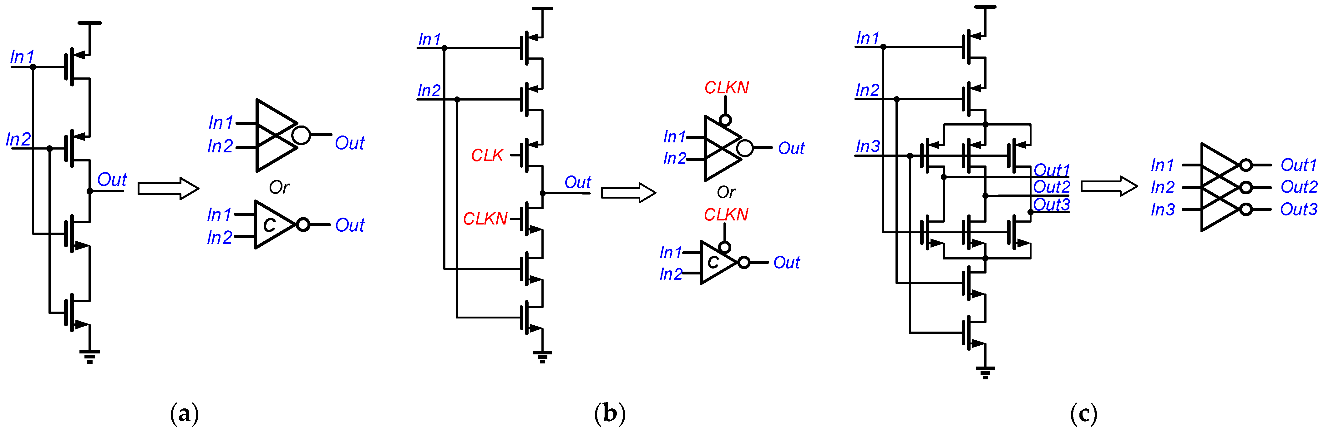
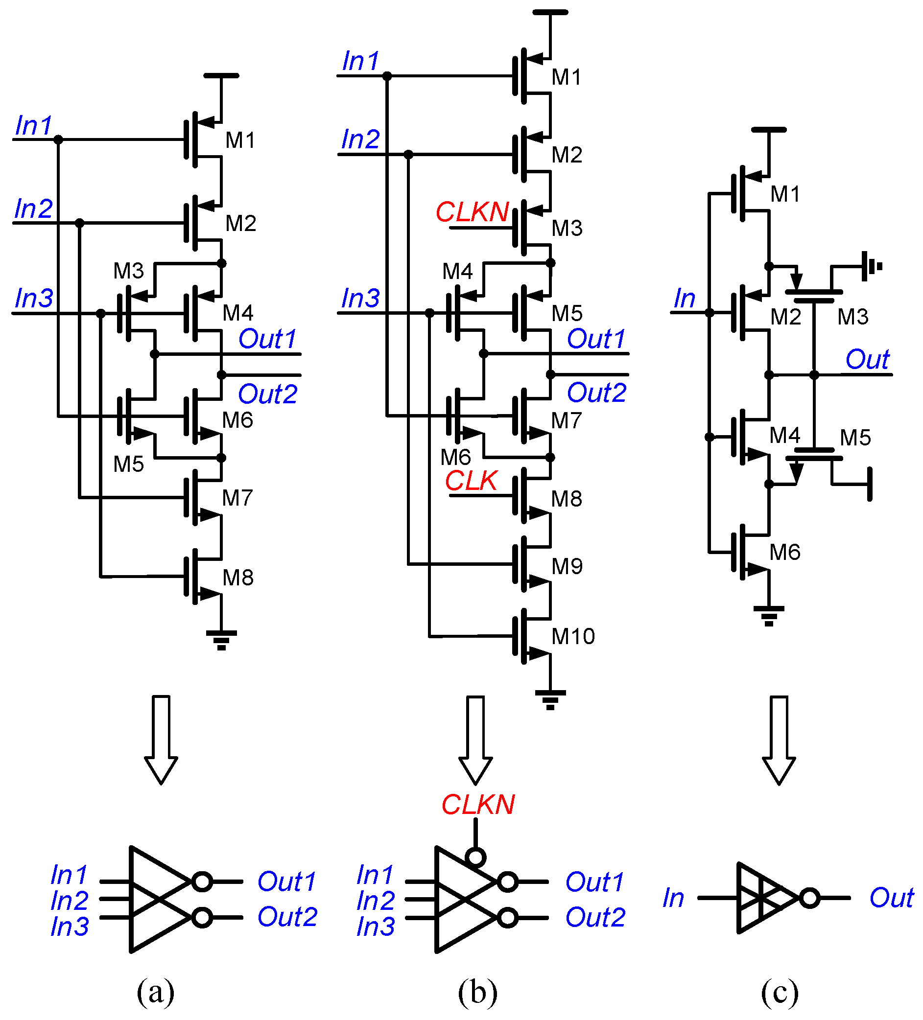
2. Previous Hardened Latch Designs
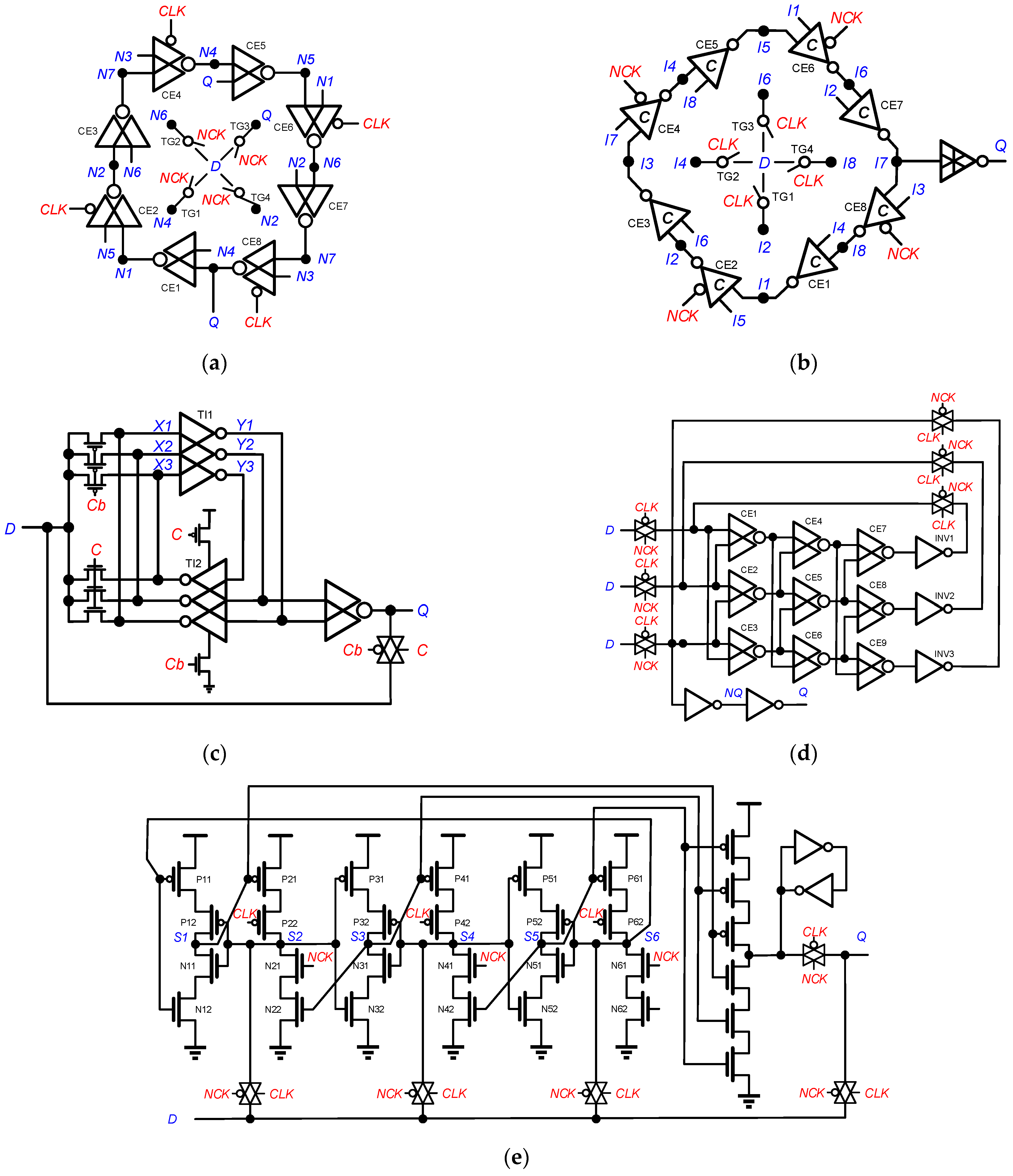
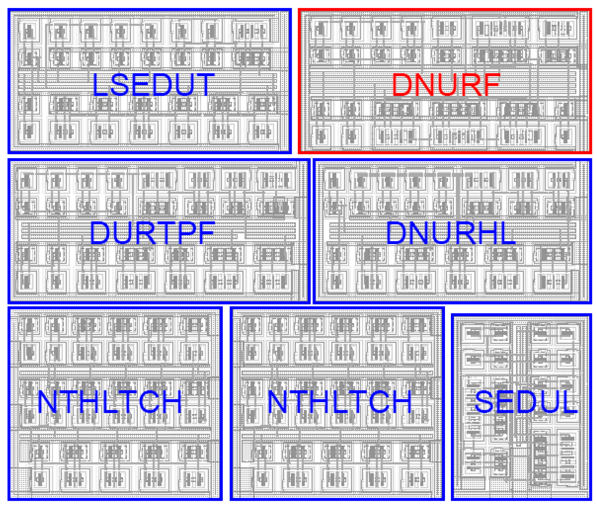
Traditionally, the RHBD technology for latches can be summarized into two main categories. One is to design new structures with SEU robustness, such as DICE [31,32]. The other is redundancy. The redundancy method includes dual modular redundancy (DMR) and triple modular redundancy (TMR) [33,34]. The output of DMR is usually composed of CEs. TMR makes three copies of the same latch structure and obtains the final logical value from a voter. The advantage of these traditional structures is that the circuit is simple and has strong SEU robustness. However, these structures are only immune to single node upset (SNU), so it is necessary to design a new latch structure that is immune to DNU.
The following section reviews several typical DNU immunity latch designs. These designs contain the DNU self-recoverable latch design for high-performance and low-power applications (DNURHL) [35], the single-event double-upset (SEDU) self-recoverable and SET pulse filterable (DURTPF) latch [36], the fast and low-power SEDU immune latch (SEDUL) [37], the non-temporarily hardened latch (NTHLTCH) [38], and the low-cost SEDU tolerant (LSEDUT) latch [39]. Figure 1 shows the subcircuit diagram and its symbols used in the latch structure above.

2.1. DNURHL

As shown in Figure 2a, the latch is primarily made up of eight mutually feeding back CEs, and any node pair of the latch is DNU self-recoverable. The latch has high performance and low power dissipation due to the use of high-speed transmission clock gating technology. However, when the node pair (N1, N5) is affected by a DNU, the state of the latch may flip.

2.2. DNUTPF

As shown in Figure 2b, the latch is mostly made up of eight CEs that give feedback on each other and a Schmitt trigger. DNURHL performs better than DNUTPF. Schmidt triggers can filter out the voltage glitch of the internal nodes of the circuit very well. However, the use of the Schmidt trigger increases the transmission delay of the circuit.

2.3. SEDUL

As shown in Figure 2c, the latch is mainly constructed from two CEs with three inputs and three outputs. The digital signal is locked into three nodes inside the circuit to improve the latch DNU’s robustness. The use of a transmission gate decreases the transmission delay of the circuit. However, when both inputs to the CE of the output stage change at the same time, the state of the latch output changes.

2.4. NTHLTCH

As shown in Figure 2d, the latch primarily consists of nine CEs and more than three inverters to build numerous feedback loops and assure DNU self-recoverability. However, the latch is not economical, particularly in terms of silicon area.

2.5. LSEDUT

As shown in Figure 2e, the latch has a three-input CE to block the soft error from the storage cell and a weak keeper to prevent a high impedance state. However, this structure has a high power consumption and cannot filter the SET pulse in the circuit well.

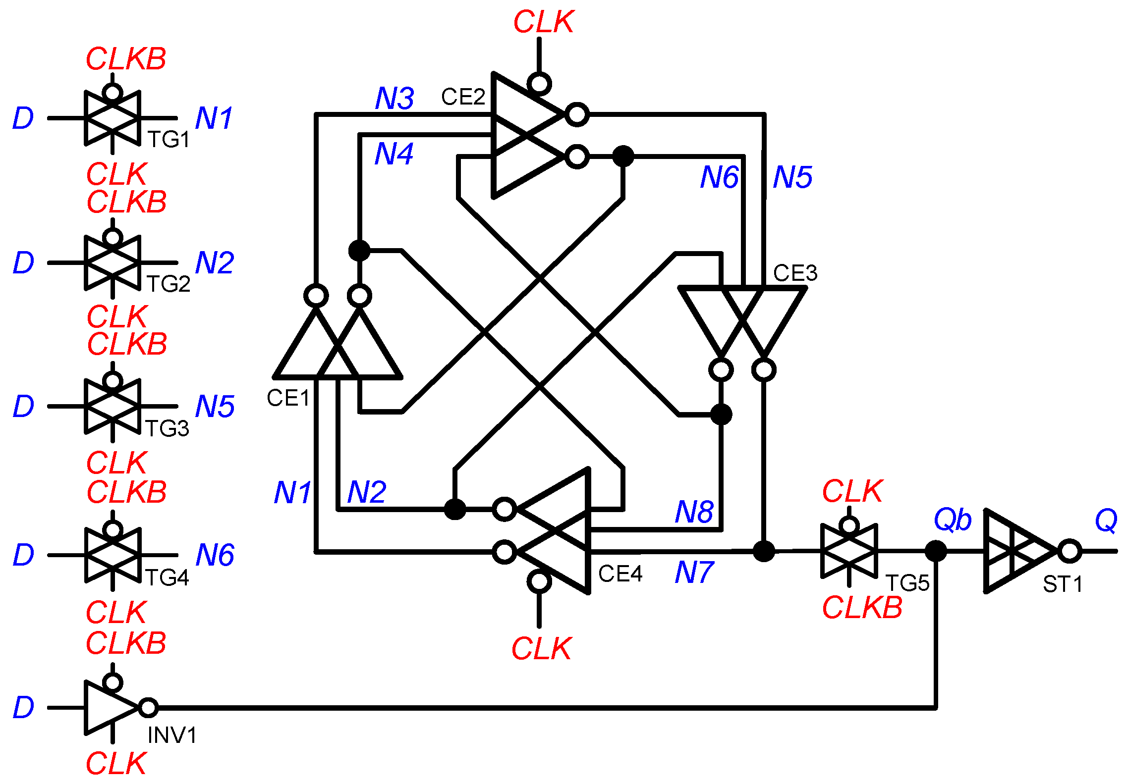
3. Proposed Hardened Latch Design

The subcircuits and symbols used in the proposed design are shown in Figure 3. The basic transmission gate and clock-controlled inverter are not included here. A CE with three inputs and two outputs is shown in Figure 3a. The states of the two outputs will change only when the three input signals flip simultaneously [40]. It is worth noting that the two outputs of the CE are separated. When one of the outputs is reversed due to a SET, the other output is not affected. A clock-controlled CE with three inputs and two outputs is shown in Figure 3b. The output state of the clock-controlled CE can only be changed when CLK is at a high level. The Schmitt trigger circuit diagram is shown in Figure 3c. The structure determines the inversion threshold and forms a hysteresis window through the positive feedback formed by M2, M3, M4, and M5. The Schmitt trigger can filter the glitch of an input signal.
Figure 4 shows the circuit diagram of the proposed design. DNURF consists of two CEs, CE1 and CE3, and two clock-controlled CEs, CE2 and CE4, five transmission gates, TG1 to TG5, a clock-controlled inverter INV1, and a Schmidt trigger ST1. The two outputs of each CE are connected to the two inputs of the next CE, and one of the outputs is also connected to the third input of the previous CE. The four CEs form a loop structure according to this connection method to ensure that the latch can self-recover from node upset. TG1 to TG4 connect input signal D to N1, N2, N5, and N6 for writing data to the latch. INV1 connects input signal D to output signal Qb, providing a fast channel from input to output. ST1 acts as the output stage to filter out transient pulses inside the circuit.

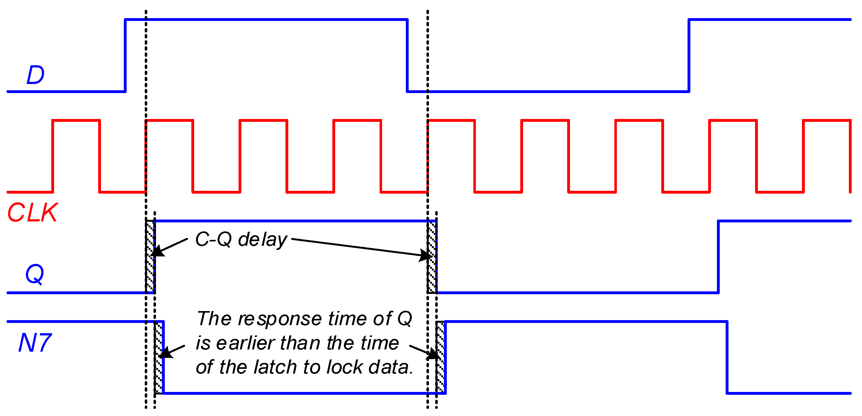
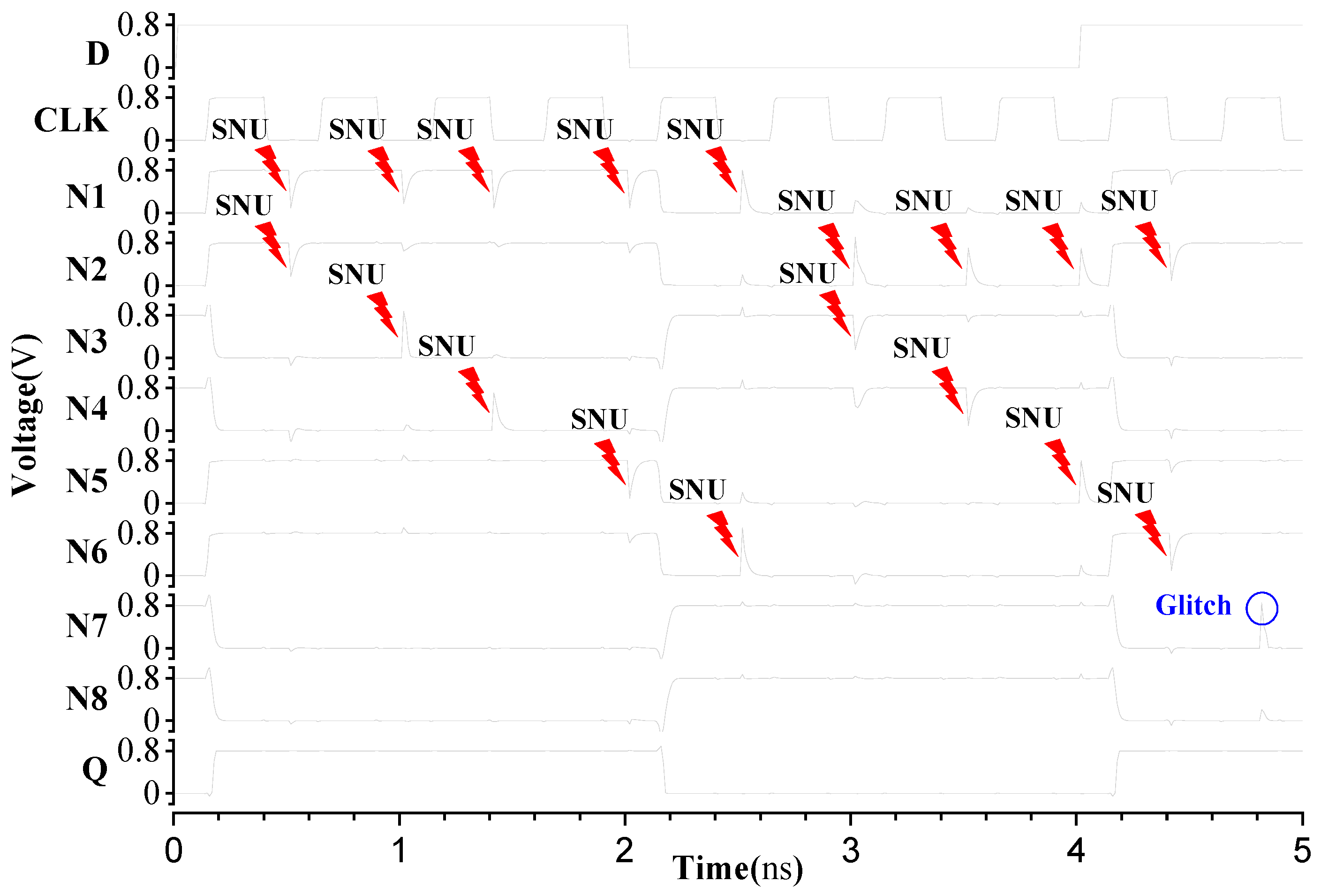
3.1. Circuit Behavior

When CLK is at a high level, and CLKN is at a low level, TG1 to TG4 are on, TG5 is off, and the latch is operating in transparent mode. Assuming that the input signal D is at a high level, the states of N1, N2, N5, and N6 are also at a high level. Since the input signals of CE1 and CE3 are determined, the states of the outputs N3, N4, N7, and N8 of CE1 and CE3 are also determined, which are at a low level. Thus, the state of all nodes inside the loop structure is determined. At this time, CE2 and CE4 are off, and the loop structure of the latch is disconnected, which reduces the power consumption of the circuit. INV1 is on, so the input signal D is transmitted through INV1 and ST1 to the output before the latch loop locks the data. This mechanism greatly reduces the latch transmission delay. Figure 5 illustrates that the response time of Q is earlier than the time of the latch to lock data.
When CLK is at a low level and CLKN is at a high level, TG1 to TG4 are off, INV1 is off, CE2 and CE4 are on, TG5 is on, and the latch is working in hold mode. The latch output no longer passes through the fast path where INV1 is located. At this time, the loop structure of the latch is closed, and all nodes can stably keep their original state unchanged, lock the data, and output it through TG5 and ST1.

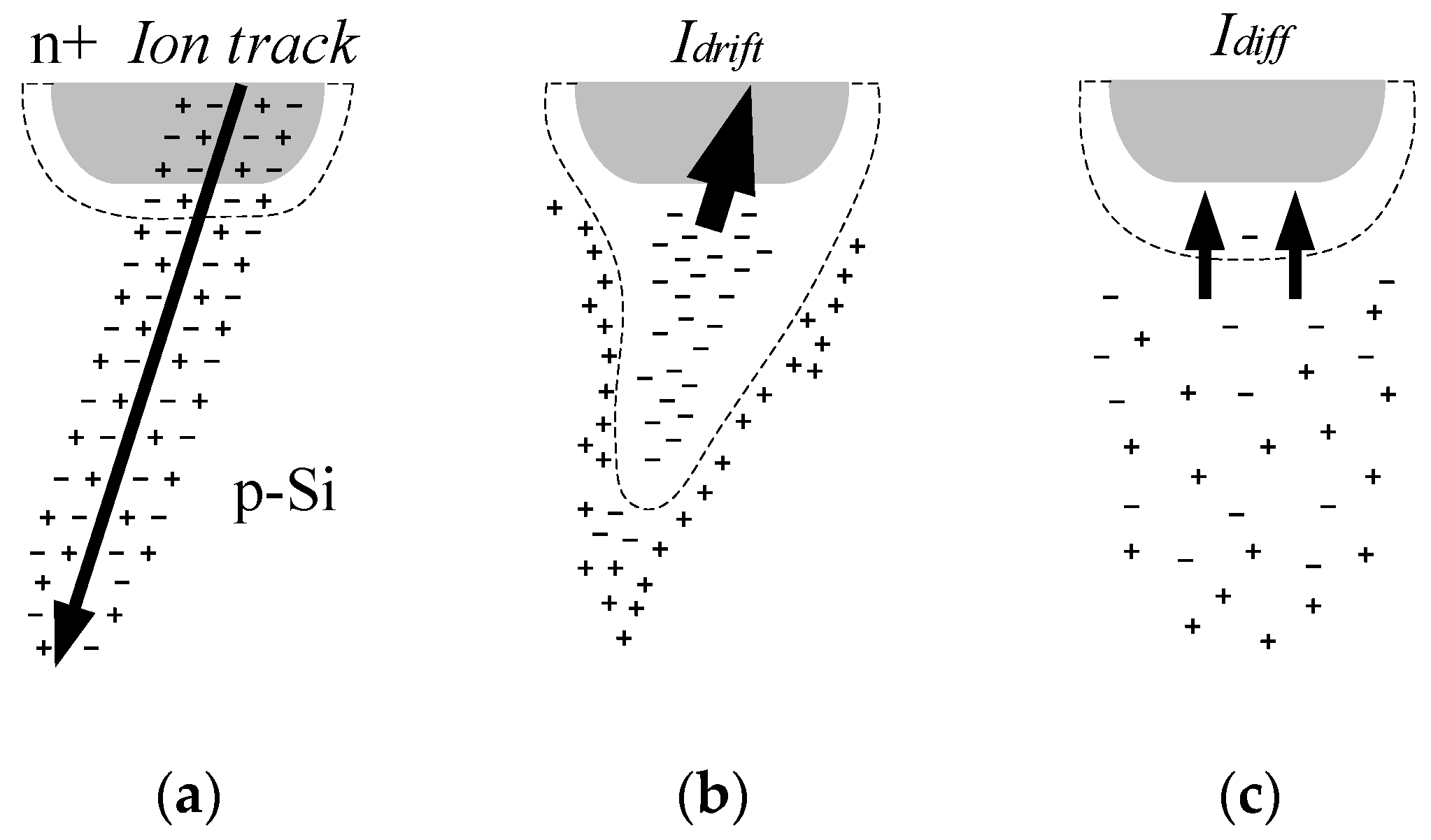
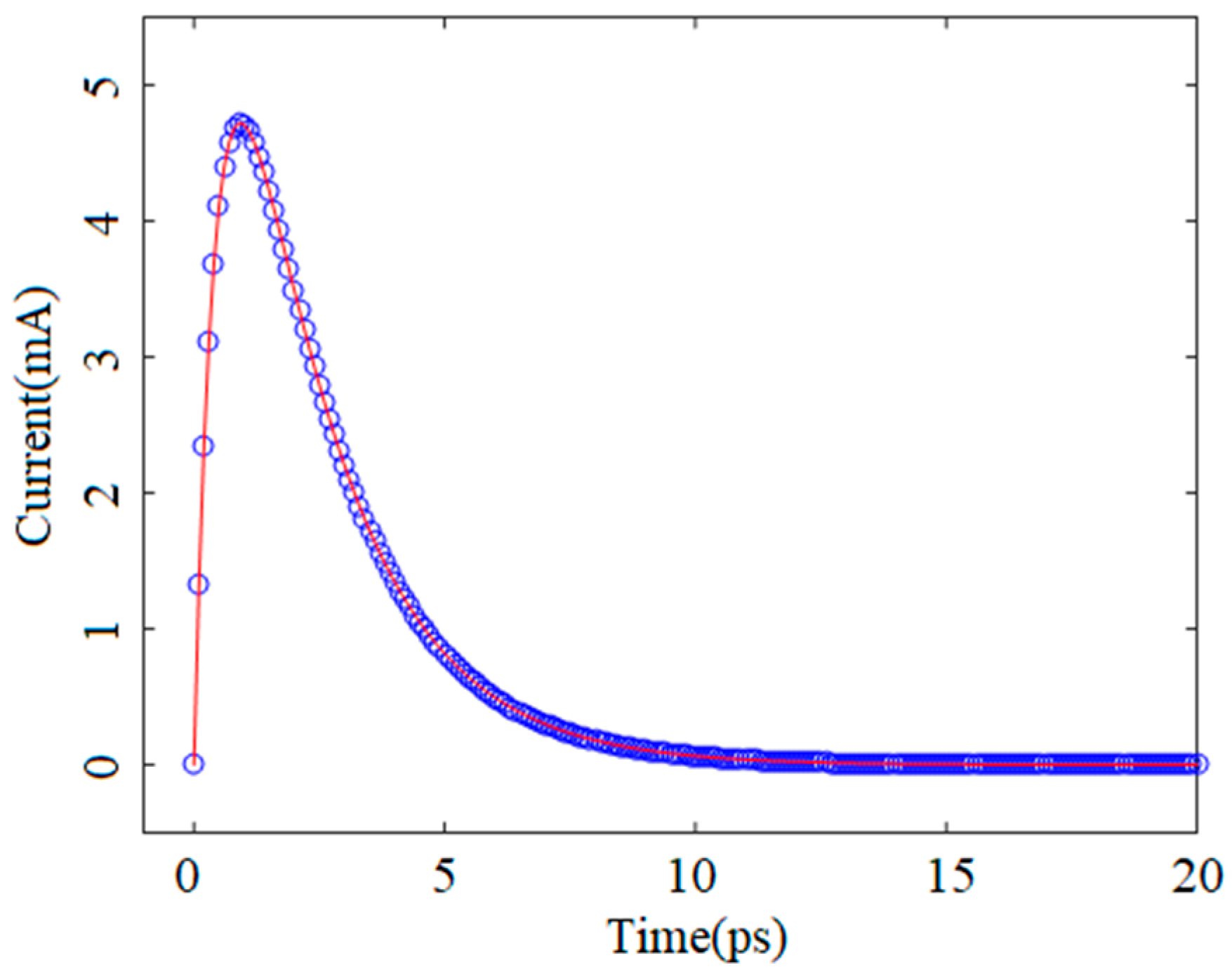
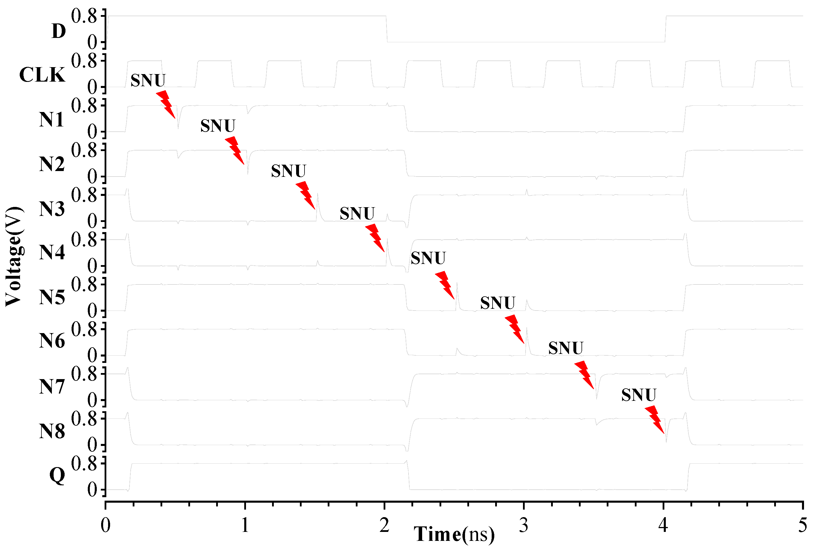
3.2. Soft Error Analysis

Before analyzing the soft error of the proposed structure, the SET mechanism is examined at the microscopic level in order to simulate SET at the circuit level. The physical process of injecting high-energy particles into sensitive nodes of transistors can be divided into three stages [41]. As shown in Figure 6a, when high-energy ions are injected into the diffusion region of transistors, a large number of electron-hole pairs will be generated, forming a cylindrical trajectory with a very high carrier concentration. When this trajectory approaches the depletion region, carriers are rapidly collected by the electric field, which generates a large transient drift current at the node and changes the potential into a funnel shape, as shown in Figure 6b. In the third stage, the diffusion current begins to dominate charge collection, as shown in Figure 6c.
Figure 7 shows the current waveforms of the sensitive nodes in the above three stages. The first stage is in the phase of carrier generation, and the node current is small. In the second stage, a large number of electron holes drift, and the node current reaches its peak. Because the charge collection process in the third stage is dominated by diffusion current, the current amplitude is relatively small, the collection time is relatively long, and the node current waveform will show a long trailing shape.
In order to model the transient current generated by particles, Messenger proposed a double exponential function model [42]. This model can well simulate the current waveform shown in Figure 7, and the expression is shown in (1).
I S E U ( t ) = I 0 ( e t τ α e t τ β )
Assuming that the amount of charge injected into the energetic particle is Qcoll, then Qcoll is the integral of I0 in the entire time domain, so the expression of Qcoll is shown in (2).
Q c o l l = 0 I 0 d ( t ) = I 0 ( τ α τ β )
By substituting (2) into (1), the complete expression of the transient current waveform, as shown in (3), can be derived.
I S E U ( t ) = Q c o l l τ α τ β ( e t τ α e t τ β )
In this paper, (3) will be used to simulate the SET of the component. In order to determine the peak value of the simulated injection transient current and the rise and fall times, a large number of papers on SET modeling have been investigated, among which the representative ones are the SET pulses fault injection model in a 130 nm CMOS process [43] and the double-exponential current source model of FinFET in a 14 nm process [44].
Figure 8a shows the waveform of transient current simulated by the TCAD tool in [43] under different LET values. It can be seen that in a 130 nm process when LET is 80 MeV·cm2/mg, the rise time of the transient current is about 25 ps, the fall time is approximately 100 ps, and the peak value is about 13 mA. Figure 8b is the waveform of the transient current simulated in [44] when the injection amount of simulated charge in the TCAD tool is 7.5 fc (equivalent to the amount of LET of 110 MeV·cm2/mg). It can be seen that in a 14 nm process, when the LET value is 110 MeV·cm2/mg, the rise time of the transient current is about 2 ps, the fall time is approximately 5 ps, and the peak current is about 4.5 mA.
It can be inferred that, under the same LET value, the rise time, fall time, and peak value of the transient current decrease with the advancement of the process. Under the same process, the rise time, fall time, and peak value of the transient current decrease as the LET value decreases. As a result, under the assumption that the LET value of the 28 nm process is 75 MeV·cm2/mg, this paper uses the transient current waveform in [44] as a reference, i.e., the transient current rising time is about 2 ps, the transient current falling time is about 5 ps, and the peak current is about 4.5 mA. Now, parameters in (3) can be reasonably selected, and the double-exponential current source waveform actually used in this paper can be obtained by using a MATLAB tool, as shown in Figure 9.
Next, the soft errors of the proposed design are analyzed. Firstly, the occurrence of SNU in DNURF is analyzed. There are eight sensitive nodes, N1 to N8, in the loop structure of DNURF. N1, N3, N5, and N7 are only used as the input of one CE, while N2, N4, N6, and N8 are used as the input of two CEs. In either case, the output state of a CE cannot be changed by an SNU at the input. For example, when N1 changes from a high level to a low level, the output of CE1 will remain at a low level. The transmission of the error signal at N1 will be blocked. At the same time, the input signals N4, N7, and N8 of CE4 keep their original low levels unchanged and will restore N1 to its original high level. Thus, DNURF is completely immune to SNU.
To evaluate the SNU immunity of the proposed design, we perform SNU simulations in the SPECTRE tool. The circuit of DNURF is implemented in 28 nm CMOS technology. All of the transistors have a W/L of 100 nm/30 nm unless otherwise stated. The supply voltage of the circuit is 0.8 V, and the clock frequency is 500 MHz. Particle injection in the circuit is simulated using the transient current shown in Figure 9.
Figure 10 shows the simulation waveforms for DNURF considering SNU on key single nodes N1 to N8. It can be seen that DNURF is completely immune to SNU at any sensitive node.
Now, consider the scenario where a node pair is affected by a DNU. There are 28 possible combinations for the eight sensitive nodes N1 to N8 of DNURF. Due to the symmetry of the DNURF structure, there are many similarities among the 28 cases. So it is unnecessary to analyze them one by one. For example, the node pairs (N1, N2), (N3, N4), (N5, N6), and (N7, N8) belong to the same situation. The node pairs (N1, N3), (N3, N5), (N5, N7), and (N7, N1) belong to the same situation.
Case D1. In the case where the node pair (N1, N2) is affected by a DNU and glitches occur, obviously, the two inputs of CE1 are mutated. Since N6 is unaffected, the states of CE1′s outputs N3 and N4 are unchanged. At the same time, only one input of CE3 is mutated, so the outputs N7 and N8 of CE3 are not affected. As a result, the DNU cannot be latched. Moreover, since the input signals N4, N7, and N8 of CE4 are intact, the node pair (N1, N2) will recover from the DNU. This analysis also applies to node pairs (N3, N4), (N5, N6), (N7, N8), (N1, N6), (N3, N8), (N5, N2), and (N7, N4).
Case D2. In the case where the node pair (N1, N3) is affected by a DNU and glitches occur, only the inputs of CE1 and CE2 are affected. Because one of the inputs to CE1 is mutated and the nodes N2 and N6 are unaffected, the transmission of glitches is blocked at CE1. Similar to the inputs of CE2, only N3 experiences a quick voltage change; hence, the voltage fluctuation of N3 cannot be transmitted further. Since the inputs of CE4 are not affected by transient pulses, the node pair (N1, N3) will recover from the DNU. This analysis also applies to node pairs (N3, N5), (N5, N7), and (N7, N1).
Case D3. In the case where the node pair (N1, N4) is affected by a DNU and glitches occur, the inputs of CE1, CE2, and CE4 are affected by the voltage glitches. Since only one input of CE1 is affected, the transmission of the voltage glitch at N1 is blocked by CE1. Similarly, the transmission of the voltage glitch at N4 is blocked by CE2 and CE4. The error signal in the loop structure cannot be latched. The node pair (N1, N4) can be restored to its original state. This analysis also applies to node pairs (N3, N6), (N5, N8), (N7, N2), (N2, N3), (N4, N5), (N6, N7), and (N8, N1).
Case D4. In the case where the node pair (N1, N5) is affected by a DNU and glitches occur, only the inputs of CE1 and CE3 are affected. One input of CE1 is mutated, while the nodes N2 and N6 are unaffected, so the outputs N3 and N4 of CE1 are unchanged. Similarly, only N5 is mutated at the input of CE3, so the outputs N7 and N8 of CE3 are unchanged. Since the inputs of CE2 and CE4 are unaffected, the node pair (N1, N5) can recover from the DNU. This analysis also applies to the node pair (N3, N7).
Case D5. The case where the node pair (N2, N4) is affected by a DNU is the worst of all. In this case, the inputs of all four CEs are affected. Because only one input of each CE is affected, the transmission of voltage glitches will be blocked by each CE. The error signal in the loop structure cannot be latched. The node pair (N2, N4) can be restored to its original state. This analysis also applies to node pairs (N4, N6), (N6, N8), and (N8, N2).
Case D6. In the case where the node pair (N2, N6) is affected by a DNU and glitches occur, it is observed that N2 and N6 are simultaneously used as inputs of CE1 and CE3. However, since the voltage of N1 and N5 does not change, the output signals N3, N4, N7, and N8 of CE1 and CE3 will remain unchanged. CE2 and CE4 can restore N2 and N6 to their original states, and the latch is self-recoverable. This analysis also applies to the node pair (N4, N8). Both combinations belong to the case where the inputs of two opposite CEs are reversed at the same time.
A double-exponential current source is used to inject current into a pair of nodes to simulate a DNU. Figure 11 shows the simulation waveforms of DNURF with DNUs, which contains all the typical cases discussed above. It can be seen that DNURF is completely immune to DNUs. It is worth mentioning that the voltage glitch generated at N7, the node closest to the output, does not have any effect on Q, which shows that DNURF can filter out the SET pulse from anywhere in the circuit.

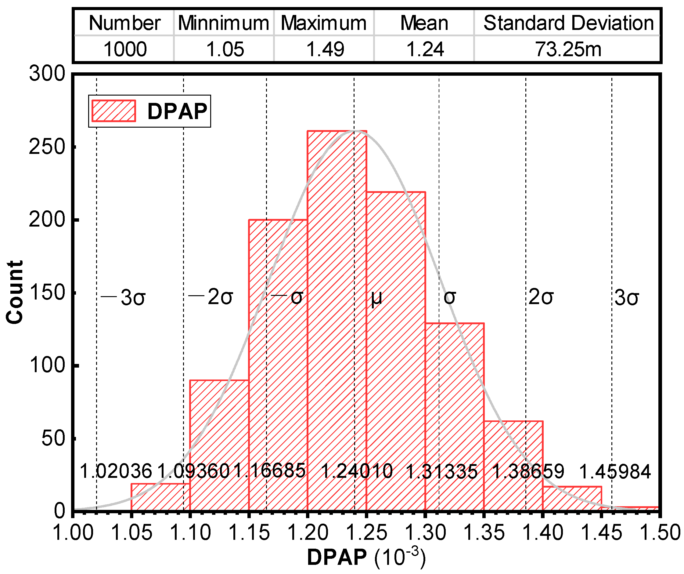
4. Performance Evaluation

In order to make a fair comparison, the proposed DNURF and the other five DNU immunity latch designs published in recent years are implemented in 28 nm CMOS technology. All transistors are the same size unless otherwise stated. A double-exponential current source is used to simulate the particle impact. The radiation hardening ability of DNURF and other contrast latch designs is measured in three aspects: whether it is DNU hardened, whether it is self-recoverable, and whether it is SET pulse filterable.
Table 1 summarizes the SEU-tolerant abilities of the proposed DNURF and the other five previous latch designs. It can be seen that all latch designs are DNU-hardened and can self-recover from a DNU. However, only DURTPF and the proposed DNURF are capable of SET pulse filtering, whereas other structures are not. In conclusion, DNURF and DURTPF have excellent radiation-hardening abilities.
The comprehensive performance of the proposed DNURF and the other five latch designs is evaluated in the following four aspects: delay, power consumption, area, and DPAP. The delay represents the delay from the rising edge of the clock to the steady state of the latch output. Power consumption is the average power consumption of the latch during a 5 ns operation. The area is the total area of all transistors and layout wiring. DPAP is the product of delay, power consumption, and area, as shown in (4). DPAP can reflect the comprehensive characteristics of the latch.
D P A P = D e l a y × P o w e r × A r e a
Table 2 shows the electrical parameters and layout area of all latch designs under the same simulation conditions. It can be seen that DURTPF and DNURF have higher latency because they use the same Schmidt trigger structure on the output side. Because DNURF establishes a fast channel from input to output, the delay of DNURF is reduced by nearly 50% compared with DURTPF. SEDUL has the lowest power consumption of 1.57 μW. LSEDUT has a maximum power consumption of 3.17 μW. The power consumption of DNURF is 2.35 μW, slightly better than DURTPF. The layout of all the latches is shown in Figure 12. The layout area of SEDUL is 16.5 μm2, which is the smallest of all the structures. The layout areas of the other structures are very similar. Compared with DURTPF, the DPAP of the proposed DNURF is improved by more than 50%.
In order to verify the effect of process variation on the proposed DNURF, Monte Carlo simulations are used in performance evaluation. To increase the reliability of the simulation results, we set the number of sampling points in Monte Carlo simulations to 1000. Figure 13 shows the Monte Carlo simulation results of DPAP on process variation. The average DPAP value of DNURF in the sample is 1.25. The standard deviation of DPAP is 73.25 m. The DPAP of the proposed DNURF is robust against process variation.

5. Conclusions

In this paper, a novel DNU self-recoverable and SET pulse filterable latch design is proposed. The proposed DNURF and five other DNU immunity latch designs published in recent years are implemented in 28 nm CMOS technology. Simulation results show that DNURF is totally immune to DNUs. DNURF has a lower transmission delay, and the DPAP is reduced by more than 50% compared with the previous design. The results of Monte Carlo simulations demonstrate that the performance of the proposed DNURF is robust against process variation.

Author Contributions

Conceptualization, S.W. and L.W.; methodology, S.W.; software, M.G.; data curation, Y.L.; writing—original draft preparation, S.W.; writing—review and editing, B.L. All authors have read and agreed to the published version of the manuscript.

Funding

This research received no external funding.

Data Availability Statement

Not applicable.

Acknowledgments

The authors would like to thank all members of the Institute of Microelectronics of the Chinese Academy of Sciences (IMECAS) for their suggestions on the circuit structure of this paper.

Conflicts of Interest

The authors declare no conflict of interest.

References

  1. Cui, X.; Zhang, Q.; Cui, X. A New Scheme of the Low-Cost Multiple-Node-Upset-Tolerant Latch. IEEE Trans. Device Mater. Reliab. 2022, 22, 50–58. [Google Scholar] [CrossRef]
  2. Schvittz, R.B.; Butzen, P.F.; da Rosa, L.S. Methods for Susceptibility Analysis of Logic Gates in the Presence of Single Event Transients. In Proceedings of the 2020 IEEE International Test Conference (ITC), Washington, DC, USA, 1–6 November 2020; pp. 1–9. [Google Scholar]
  3. Hamed, E.A.; Lee, I. Categorization and SEU Fault Simulations of Radiation-Hardened-by-Design Flip-Flops. Electronics 2021, 10, 1572. [Google Scholar] [CrossRef]
  4. Schrape, O.; Andjelković, M.; Breitenreiter, A.; Zeidler, S.; Balashov, A.; Krstić, M. Design and evaluation of radiation-hardened standard cell flip-flops. IEEE Trans. Circuits Syst. I Regul. Pap. 2021, 68, 4796–4809. [Google Scholar] [CrossRef]
  5. Kumar, C.I.; Anand, B. A highly reliable and energy efficient radiation hardened 12T SRAM cell design. IEEE Trans. Device Mater. Reliab. 2019, 20, 58–66. [Google Scholar] [CrossRef]
  6. Gadlage, M.J.; Roach, A.H.; Duncan, A.R.; Williams, A.M.; Bossev, D.P.; Kay, M.J. Soft errors induced by high-energy electrons. IEEE Trans. Device Mater. Reliab. 2016, 17, 157–162. [Google Scholar] [CrossRef]
  7. Dodd, P.E.; Massengill, L.W. Basic mechanisms and modeling of single-event upset in digital microelectronics. IEEE Trans. Nucl. Sci. 2003, 50, 583–602. [Google Scholar] [CrossRef]
  8. Teifel, J. Self-voting dual-modular-redundancy circuits for single-event-transient mitigation. IEEE Trans. Nucl. Sci. 2008, 55, 3435–3439. [Google Scholar] [CrossRef]
  9. Sajjade, F.M.; Goyal, N.K.; Varaprasad, B. Single event transient (SET) mitigation circuits with immune leaf nodes. IEEE Trans. Device Mater. Reliab. 2021, 21, 70–78. [Google Scholar] [CrossRef]
  10. Watkins, A.; Tragoudas, S. Radiation hardened latch designs for double and triple node upsets. IEEE Trans. Emerg. Top. Comput. 2017, 8, 616–626. [Google Scholar] [CrossRef]
  11. Amirany, A.; Marvi, F.; Jafari, K.; Rajaei, R. Nonvolatile spin-based radiation hardened retention latch and flip-flop. IEEE Trans. Nanotechnol. 2019, 18, 1089–1096. [Google Scholar] [CrossRef]
  12. Li, T.; Liu, H.; Yang, H. Design and characterization of SEU hardened circuits for SRAM-based FPGA. IEEE Trans. Very Large Scale Integr. VLSI Syst. 2019, 27, 1276–1283. [Google Scholar] [CrossRef]
  13. Amirany, A.; Jafari, K.; Moaiyeri, M.H. High-performance radiation-hardened spintronic retention latch and flip-flop for highly reliable processors. IEEE Trans. Device Mater. Reliab. 2021, 21, 215–223. [Google Scholar] [CrossRef]
  14. Li, J.; Xiao, L.; Li, H.; Cao, X.; Wang, C. A Soft Error Detection and Recovery Flip-Flop for Aggressive Designs with High-Performance. IEEE Trans. Device Mater. Reliab. 2022, 22, 223–231. [Google Scholar] [CrossRef]
  15. Wang, S.; Wang, L.; Wang, Y.; Guo, M.; Li, Y. A Novel Radiation-Hardened CCDM-TSPC Compared with Seven Well-Known RHBD Flip-Flops in 180 nm CMOS Process. Electronics 2022, 11, 3098. [Google Scholar] [CrossRef]
  16. Pal, S.; Sri, D.D.; Ki, W.-H.; Islam, A. Soft-error resilient read decoupled SRAM with multi-node upset recovery for space applications. IEEE Trans. Electron Devices 2021, 68, 2246–2254. [Google Scholar] [CrossRef]
  17. Pal, S.; Ki, W.-H.; Tsui, C.-Y. Soft-error-aware read-stability-enhanced low-power 12T SRAM with multi-node upset recoverability for aerospace applications. IEEE Trans. Circuits Syst. I Regul. Pap. 2022, 69, 1560–1570. [Google Scholar] [CrossRef]
  18. Eftaxiopoulos, N.; Axelos, N.; Zervakis, G.; Tsoumanis, K.; Pekmestzi, K. Delta DICE: A double node upset resilient latch. In Proceedings of the 2015 IEEE 58th International Midwest Symposium on Circuits and Systems (MWSCAS), Fort Collins, CO, USA, 2–5 August 2015; pp. 1–4. [Google Scholar]
  19. Yan, A.; Huang, Z.; Yi, M.; Xu, X.; Ouyang, Y.; Liang, H. Double-node-upset-resilient latch design for nanoscale CMOS technology. IEEE Trans. Very Large Scale Integr. VLSI Syst. 2017, 25, 1978–1982. [Google Scholar] [CrossRef]
  20. He, Q.; Yan, A.; Lai, C.; Zhang, Y.; Liu, C.; Chen, Z.; Wu, Z.; Cui, J.; Liang, H. Novel low cost and DNU online self-recoverable RHBD latch design for nanoscale CMOS. In Proceedings of the 2018 IEEE International Symposium on Circuits and Systems (ISCAS), Florence, Italy, 27–30 May 2018; pp. 1–5. [Google Scholar]
  21. Yamamoto, Y.; Namba, K. Construction of latch design with complete double node upset tolerant capability using C-element. In Proceedings of the 2018 IEEE International Symposium on Defect and Fault Tolerance in VLSI and Nanotechnology Systems (DFT), Chicago, IL, USA, 8–10 October 2018; pp. 1–6. [Google Scholar]
  22. Li, Y.; Cheng, X.; Tan, C.; Han, J.; Zhao, Y.; Wang, L.; Li, T.; Tahoori, M.B.; Zeng, X. A robust hardened latch featuring tolerance to double-node-upset in 28nm CMOS for spaceborne application. IEEE Trans. Circuits Syst. II Express Briefs 2020, 67, 1619–1623. [Google Scholar] [CrossRef]
  23. Guo, J.; Liu, S.; Zhu, L.; Lombardi, F. Design and evaluation of low-complexity radiation hardened CMOS latch for double-node upset tolerance. IEEE Trans. Circuits Syst. I Regul. Pap. 2020, 67, 1925–1935. [Google Scholar] [CrossRef]
  24. Guo, J.; Liu, S.; Su, X.; Qi, C.; Lombardi, F. High-performance CMOS latch designs for recovering all single and double node upsets. IEEE Trans. Aerosp. Electron. Syst. 2021, 57, 4401–4415. [Google Scholar] [CrossRef]
  25. Eftaxiopoulos, N.; Axelos, N.; Pekmestzi, K. DONUT: A double node upset tolerant latch. In Proceedings of the 2015 IEEE Computer Society Annual Symposium on VLSI, Montpellier, France, 8–10 July 2015; pp. 509–514. [Google Scholar]
  26. Yan, A.; Chen, Y.; Xu, Z.; Chen, Z.; Cui, J.; Huang, Z.; Patrick, G.; Wen, X. Design of double-upset recoverable and transient-pulse filterable latches for low-power and low-orbit aerospace applications. IEEE Trans. Aerosp. Electron. Syst. 2020, 56, 3931–3940. [Google Scholar] [CrossRef]
  27. Li, T.; Chen, L.; Jensen, C.S.; Pedersen, T.B.; Gao, Y.; Hu, J. Evolutionary clustering of moving objects. In Proceedings of the IEEE 38th International Conference on Data Engineering (ICDE), Kuala Lumpur, Malaysia, 9–12 May 2022; pp. 2399–2411. [Google Scholar]
  28. Zhang, N.; Sun, Q.; Yang, L.; Li, Y. Event-triggered distributed hybrid control scheme for the integrated energy system. IEEE Trans. Ind. Inf. 2021, 18, 835–846. [Google Scholar] [CrossRef]
  29. Yang, L.; Li, X.; Sun, M.; Sun, C. Hybrid policy-based reinforcement learning of adaptive energy management for the Energy transmission-constrained island group. IEEE Trans. Ind. Inf. 2023. early access. [Google Scholar] [CrossRef]
  30. Bourdarie, S.; Xapsos, M. The near-earth space radiation environment. IEEE Trans. Nucl. Sci. 2008, 55, 1810–1832. [Google Scholar] [CrossRef] [Green Version]
  31. Wang, H.-B.; Li, Y.-Q.; Chen, L.; Li, L.-X.; Liu, R.; Baeg, S.; Mahatme, N.; Bhuva, B.; Wen, S.-J.; Wong, R. An SEU-tolerant DICE latch design with feedback transistors. IEEE Trans. Nucl. Sci. 2015, 62, 548–554. [Google Scholar] [CrossRef]
  32. Hatefinasab, S.; Ohata, A.; Salinas, A.; Castillo, E.; Rodriguez, N. Highly Reliable Quadruple-Node Upset-Tolerant D-Latch. IEEE Access 2022, 10, 31836–31850. [Google Scholar] [CrossRef]
  33. Furuta, J.; Hamanaka, C.; Kobayashi, K.; Onodera, H. A 65nm bistable cross-coupled dual modular redundancy Flip-Flop capable of protecting soft errors on the C-element. In Proceedings of the Symposium on VLSI Circuits, Honolulu, HI, USA, 16–18 June 2010; pp. 123–124. [Google Scholar]
  34. Lyons, R.E.; Vanderkulk, W. The use of triple-modular redundancy to improve computer reliability. IBM J. Res. Dev. 1962, 6, 200–209. [Google Scholar] [CrossRef] [Green Version]
  35. Yan, A.; Yang, K.; Huang, Z.; Zhang, J.; Cui, J.; Fang, X.; Yi, M.; Wen, X. A double-node-upset self-recoverable latch design for high performance and low power application. IEEE Trans. Circuits Syst. II Express Briefs 2018, 66, 287–291. [Google Scholar] [CrossRef]
  36. Yan, A.; Hu, Y.; Song, J.; Wen, X. Single-event double-upset self-recoverable and single-event transient pulse filterable latch design for low power applications. In Proceedings of the 2019 Design, Automation & Test in Europe Conference & Exhibition (DATE), Florence, Italy, 25–29 March 2019; pp. 1679–1684. [Google Scholar]
  37. Rajaei, R.; Niemier, M.; Hu, X.S. Low-Cost Sequential Logic Circuit Design Considering Single Event Double-Node Upsets and Single Event Transients. In Proceedings of the 2021 IEEE 39th International Conference on Computer Design (ICCD), Storrs, CT, USA, 24–27 October 2021; pp. 178–185. [Google Scholar]
  38. Li, Y.; Wang, H.; Yao, S.; Yan, X.; Gao, Z.; Xu, J. Double node upsets hardened latch circuits. J. Electron. Test. 2015, 31, 537–548. [Google Scholar] [CrossRef]
  39. Jiang, J.; Xu, Y.; Ren, J.; Zhu, W.; Lin, D.; Xiao, J.; Kong, W.; Zou, S. Low-cost single event double-upset tolerant latch design. Electron. Lett. 2018, 54, 554–556. [Google Scholar] [CrossRef]
  40. Shams, M.; Ebergen, J.C.; Elmasry, M.I. Modeling and comparing CMOS implementations of the C-element. IEEE Trans. Very Large Scale Integr. VLSI Syst. 1998, 6, 563–567. [Google Scholar] [CrossRef]
  41. Baumann, R.C. Radiation-induced soft errors in advanced semiconductor technologies. IEEE Trans. Device Mater. Reliab. 2005, 5, 305–316. [Google Scholar] [CrossRef]
  42. Messenger, G. Collection of charge on junction nodes from ion tracks. IEEE Trans. Nucl. Sci. 1982, 29, 2024–2031. [Google Scholar] [CrossRef]
  43. Xu, C.; Liu, Y.; Weng, X.; Li, Z.; Yang, Y. Single event transient pulses fault injection model based on LET for circuit-level simulation. In Proceedings of the IEEE 15th International Conference on Solid-State & Integrated Circuit Technology (ICSICT), Kunming, China, 3–6 November 2020; pp. 1–3. [Google Scholar]
  44. Liu, B.; Zhang, S.; Li, C. Composite double exponential current source model for single event transient in 14 nm SOI FinFET. Res. Prog. SSE 2022, 42, 93–98. [Google Scholar]
Figure 1. Components used in the previous design: (a) two inputs CE; (b) clock-controlled two inputs CE; (c) three inputs and three outputs CE.
Electronics 12 01193 g001
Figure 2. Schematics of the reviewed latch designs: (a) DNURHL; (b) DNUTPF; (c) SEDUL; (d) NTHLTCH; (e) LSEDUT.
Electronics 12 01193 g002
Figure 3. Components used in the proposed design: (a) three inputs and two outputs CE; (b) clock-controlled three inputs and two outputs CE; (c) Schmitt trigger.
Electronics 12 01193 g003
Figure 4. Circuit diagram of the proposed design DNURF.
Electronics 12 01193 g004
Figure 5. Operation waveform of the proposed design DNURF.
Electronics 12 01193 g005
Figure 6. Three stages of injecting high-energy particles into sensitive nodes of transistors: (a) carrier generation; (b) carrier drift; (c) carrier diffusion.
Electronics 12 01193 g006
Figure 7. Three stages of transient current of transistor sensitive nodes.
Electronics 12 01193 g007
Figure 8. Current source model for SET in different processes: (a) 130 nm process; (b) 14 nm process.
Electronics 12 01193 g008
Figure 9. The current waveform used to simulate SET in this paper.
Electronics 12 01193 g009
Figure 10. Simulation waveforms for DNURF considering SNU on key single nodes N1 to N8.
Electronics 12 01193 g010
Figure 11. Simulation waveforms for DNURF considering DNU on representative node pairs.
Electronics 12 01193 g011
Figure 12. Layout of the proposed DNURF and the other five DNU tolerant latch designs.
Electronics 12 01193 g012
Figure 13. Monte Carlo simulation results of DPAP on process variation.
Electronics 12 01193 g013
Table 1. Robustness comparison of the proposed DNURF with existing hardened latches.
Latch NameDNU TolerantSelf-RecoverableSet Pulse Filterable
DNURHL [35]OKOKNo
DURTPF [36]OKOKOK
SEDUL [37]OKOKNo
NTHLTCH [38]OKOKNo
LSEDUT [39]OKOKNo
This workOKOKOK
Table 2. Cost comparison of the proposed DNURF with existing hardened latches.
Latch NameDelay (ps)Power (μW)Area (μm2)DPAP (10−3)
DNURHL [35]3.672.2525.950.21
DURTPF [36]37.872.4828.312.66
SEDUL [37]2.111.5716.50.05
NTHLTCH [38]14.322.4426.960.94
LSEDUT [39]2.423.1726.440.2
This work18.922.3527.751.23
Disclaimer/Publisher’s Note: The statements, opinions and data contained in all publications are solely those of the individual author(s) and contributor(s) and not of MDPI and/or the editor(s). MDPI and/or the editor(s) disclaim responsibility for any injury to people or property resulting from any ideas, methods, instructions or products referred to in the content.

