1. Introduction
Electronic equipment is widely used in industry, commerce, and households. It is generally powered by the utility through an AC-DC power conversion interface. Over the last two decades, batteries have started from powering our portable electronics to powering our vehicles and household equipment, such as robot vacuums, electric bikes, mowing machines, etc. With the development of robots and electric vehicles, the number of battery-powered devices has increased dramatically. Those batteries have to be charged from the utility through an AC-DC power conversion interface.
In order to keep good power quality for electronic equipment and ensure the performance of battery sets, an AC-DC power conversion interface must provide a stable and controllable voltage/current at the DC port and produce a sinusoidal input current at the AC port with nearly a unit power factor. Diode rectifiers do not meet these requirements and cannot work as an AC-DC power conversion interface alone [
1]. Due to the price decrease in the power semiconductor components and advanced switching power supply technology, active power factor correction (PFC) rectifiers have been well-developed. Conventionally, a switching power converter, such as a boost, buck, or buck–boost converter, is connected to the DC port of a diode rectifier for a single-phase PFC circuit [
1,
2,
3,
4,
5,
6]. The diode rectifier converts the utility voltage into a rectified voltage, which is then further converted into a controllable DC voltage/current through a switching power converter. The switching power converter also shapes the input current for a good power factor and low current harmonic distortion.
Different from discontinuous input current driven by buck converter or buck–boost converter, boost converter drives its input current continuously, which eliminates the large-capacity input filter and reduces electromagnetic interference (EMI). In order to improve the power efficiency of PFC circuit, the bridgeless PFC circuit integrates the diode bridge and the boost converter to eliminate one rectifier diode voltage drop at the forward path [
7,
8]. However, the DC output voltage for a PFC circuit that uses a boost converter is always greater than the amplitude of the utility voltage. Hence, a buck converter with a high step-down ratio is required for low-voltage applications, and the overall power efficiency is low. To reduce leakage current and increase the step-down ratio, an isolated converter, such as a flyback or forward converter, is connected to the diode rectifier in the PFC circuit [
9,
10,
11]. However, this produces a discontinuous input current and results in high voltage stress for power electronic switches. Moreover, the use of a transformer also decreases the power efficiency and induces spike voltages.
Power semiconductor components are worked as switches for power conversion applications. Their non-ideal switching characteristics induce switching losses during the switching turned-on and turned-off transitions. The switching loss is highly dependent on the transition time, transition voltage/current level, and semiconductor switching characteristics. For the switching power converter used in the conventional PFC circuit, the power semiconductor components are operated in hard switching with a high transition voltage level, resulting in a large switching loss. Soft switching technologies, which take advantage of the LC resonant to turn the switch components at nearly zero transition voltage/current level, can reduce switching losses dramatically [
12,
13,
14]. However, most soft switching technologies significantly increase the complexity of the controller and power circuit design. In addition, the resonant performance is heavily affected by the drift of passive components.
Multi-level converters (MLCs) reduce the transition voltage level of the switching of power electronic switches, so both the switching harmonics and the switching loss are reduced. Therefore, the capacities of both passive filter components and heat dissipation components can be effectively reduced. The diode-clamped MLCs employ a number of clamped diodes as the conduction paths to generate more output voltage levels and reduce the transition voltage level of the power electronic switches [
15,
16]. However, these clamped diodes have higher voltage ratings and result in larger power losses. The flying-capacitor MLCs generate more output voltage levels and reduce the switching voltages of power electronic switches by inserting capacitors into the conduction path [
17,
18]. However, these capacitors enlarge the circuit volume. In addition, the issues of voltage balance in both diode-clamped MLCs and flying-capacitor MLCs have to be concerned [
15,
16,
17,
18]. The cascaded bridge MLCs connect several full-bridge converters (FBCs) to generate more output voltage levels and reduce the switching voltages of power electronic switches [
19,
20,
21,
22,
23]. An independent DC source is necessary for each FBC, which is the primary consideration for cascaded bridge MLCs. Although most MLCs are applied in DC-AC power conversions, many AC-DC power conversion applications have been developed in recent years [
24,
25,
26,
27].
In order to keep the advantage of the continuous input current of the boost-type PFC circuits but eliminate the drawback of the high step-down ratio of the second stage and high transition voltage level, this paper proposes a cascaded AC-DC power conversion interface (CADPCI) to convert AC power from the utility into stable DC power to charge the battery set. The proposed CADPCI is composed of a cascaded converter (CC) and a dual-input buck converter (DIBC). The major contributions of the proposed CADPCI are listed as follows.
The CC uses an FBC and a bridgeless rectifier (BLR), connected in series, to generate an 11-level input voltage and perform a unity power factor. Only six power electronic switches are used in the CC.
The switching loss of the CC is reduced significantly because only the FBC with a lower DC port voltage is switched at a high frequency.
The DIBC controls the DC port voltage of the BLR to achieve a power balance between the BLR and the utility. The FBC does not handle real power to save an isolated converter for regulating the DC port voltage of the FBC, thus simplifying the power circuit of the CC.
DIBC further realizes the function of a DC active filter (DAF) with no additional circuit.
This paper is organized as follows:
Section 2 reviews the cascaded converter in rectifier applications, followed by the principle of the proposed cascaded power conversion interface in
Section 3. Then,
Section 4 describes the operation of the proposed dual-input buck converter, and
Section 5 explains the operation of the cascaded converter. The last two sections show the experimental results and conclude this paper.
2. Cascaded Converter
The CC is configured by connecting several FBCs in series, as shown in
Figure 1. According to the DC port voltage of different FBCs, the CC is divided into symmetrical CC and asymmetrical CC. The DC port voltages of the FBCs in a symmetrical CC are always the same. The symmetrical CC has 2
n + 1 voltage levels at the AC port, where
n is the number of FBCs [
19,
20]. The benefits of symmetrical CC include easily modulated and even distribution of the power losses. On the other hand, the DC port voltages of the FBCs in an asymmetrical CC are usually in multiple relationships. Accordingly, the asymmetric CC generates more levels of AC port voltage compared to the symmetrical CC [
21,
22,
23]. The CCs with two FBCs are given as examples. A two-FBCs symmetrical CC generates five voltage levels at the AC port. A two-FBC asymmetrical CC, which has a 1:2 voltage ratio at their FBC DC port voltages, generates seven voltage levels at the AC port [
22]. A two-FBC asymmetrical CC, which has a 1:3 voltage ratio at their FBC DC port voltages, generates nine voltage levels at the AC port [
23].
Regardless of symmetrical or asymmetrical CC, each FBC requires an independent DC power supply, which increases the complexity of the DC power processing circuit.
3. Principle of Proposed Cascaded Power Conversion Interface
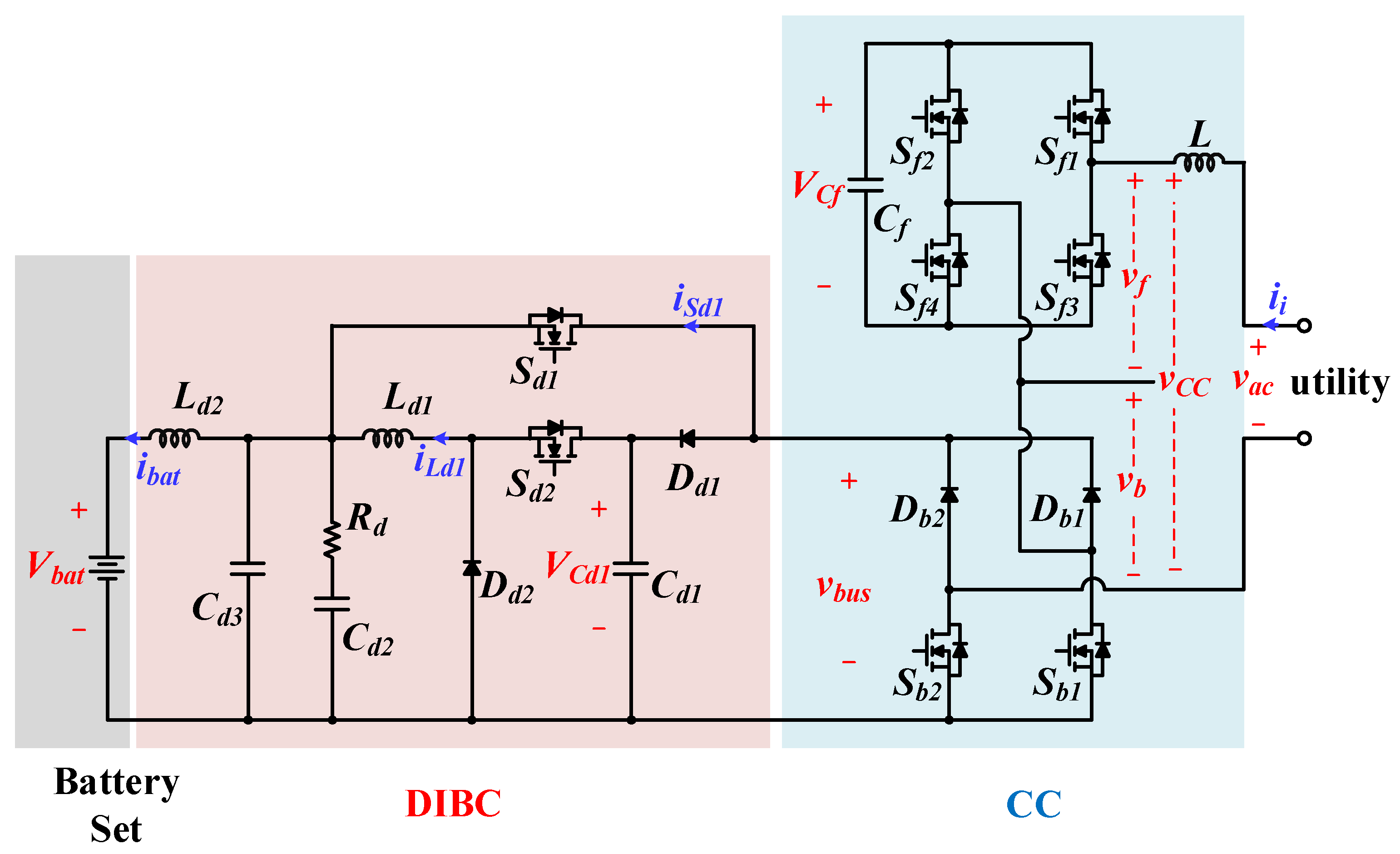
The power circuit of the proposed CADPCI is shown in
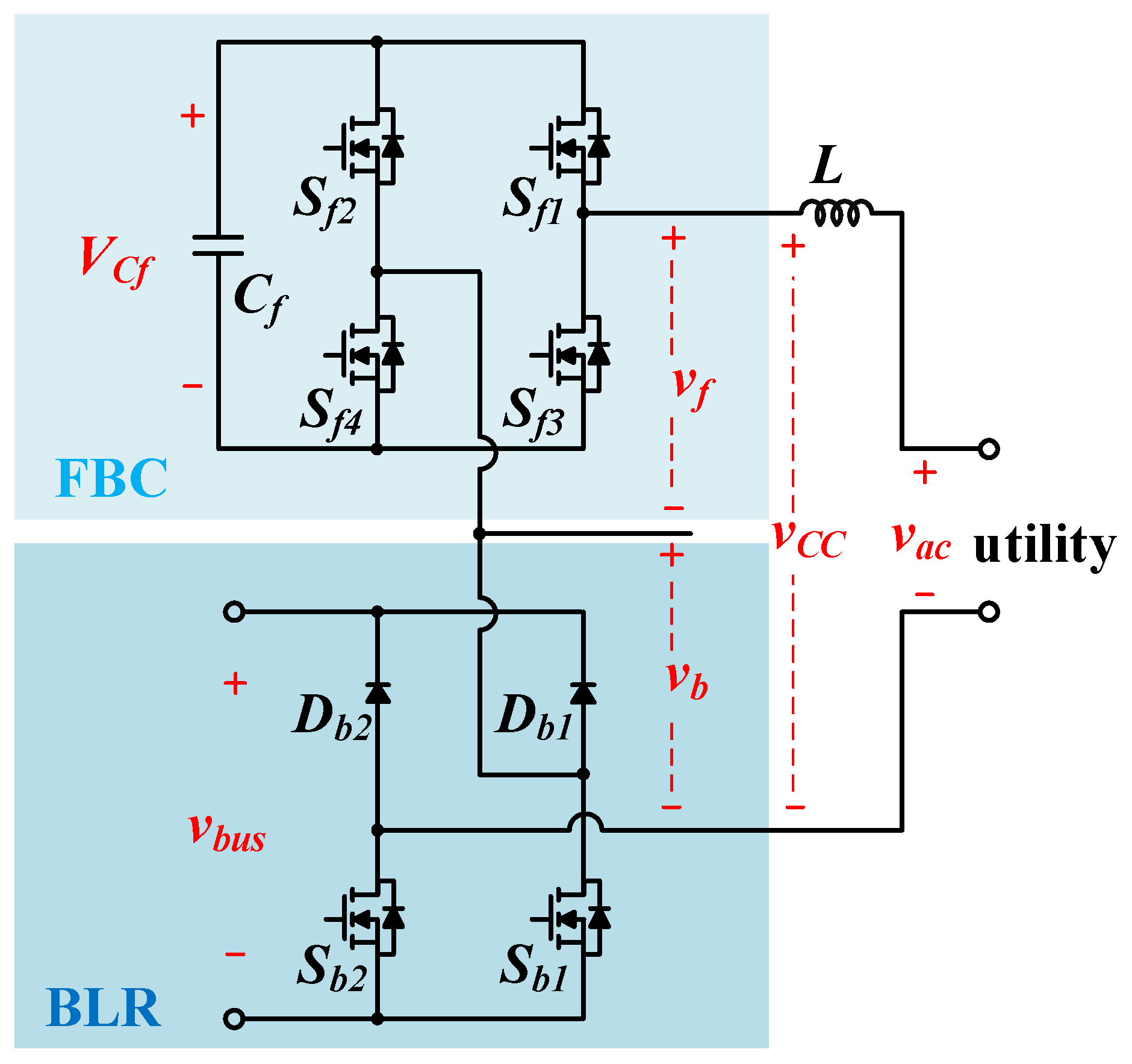
Figure 2. The proposed CADPCI is composed of a CC and a DIBC. The CC combines an FBC and a BLR in a series connection, as shown in
Figure 3. The BLR replaces the diode rectifier of the PFC circuit to decrease conduction loss [
7,
8], but an extra switch component is necessary. The FBC uses unipolar pulse width modulation (PWM) to control power switches
Sf1–
Sf4 to generate a three-level pulse voltage at the AC port of the FBC (
vf). The DC port of the BLR is connected to the DIBC. The DIBC integrates a buck converter and a selector switch (
Sd1) to provide a two-level DC voltage to the DC port of the BLR. The power switches
Sb1 and
Sb2 of BLR are switched synchronously with the utility voltage to generate a five-level step-wave voltage at the AC port of the BLR (
vb). The two-level DC voltage for the DC port of the BLR is two or four times the DC port voltage of the FBC (
VCf). Therefore, the proposed CC can synthesize an 11-level input voltage by cascading the ac port voltages of FBC and BLR. Compared to the asymmetrical CC with two FBCs, the proposed CC can generate more voltage levels. The CC also produces a sinusoidal input current to perform a unity power factor. The FBC with a low DC port voltage is the only part switching in high frequency.
The DIBC also performs the function of DAF with no additional circuit to filter out low-frequency ripple of the charging current. A low-pass filter that is configured using Cd2, Cd3, Rd, and Ld2 is used to filter out the switching ripple of the charging current.
4. Operation of Dual-Input Buck Converter
Although the CADPCI performs unity power factor correction, the instantaneous input power from the utility includes not only a DC power but also a twice-utility-frequency AC power. The twice-utility-frequency AC power results in a ripple current on the DC side of the CADPCI that charges the battery set. This ripple current may reduce the life of the battery set [
28,
29]. The novelty of the DIBC is that the buck converter in the DIBC not only regulates the DC port voltage of the BLR but also acts as a DAF to filter out low-frequency ripple of the charging current for the battery set.
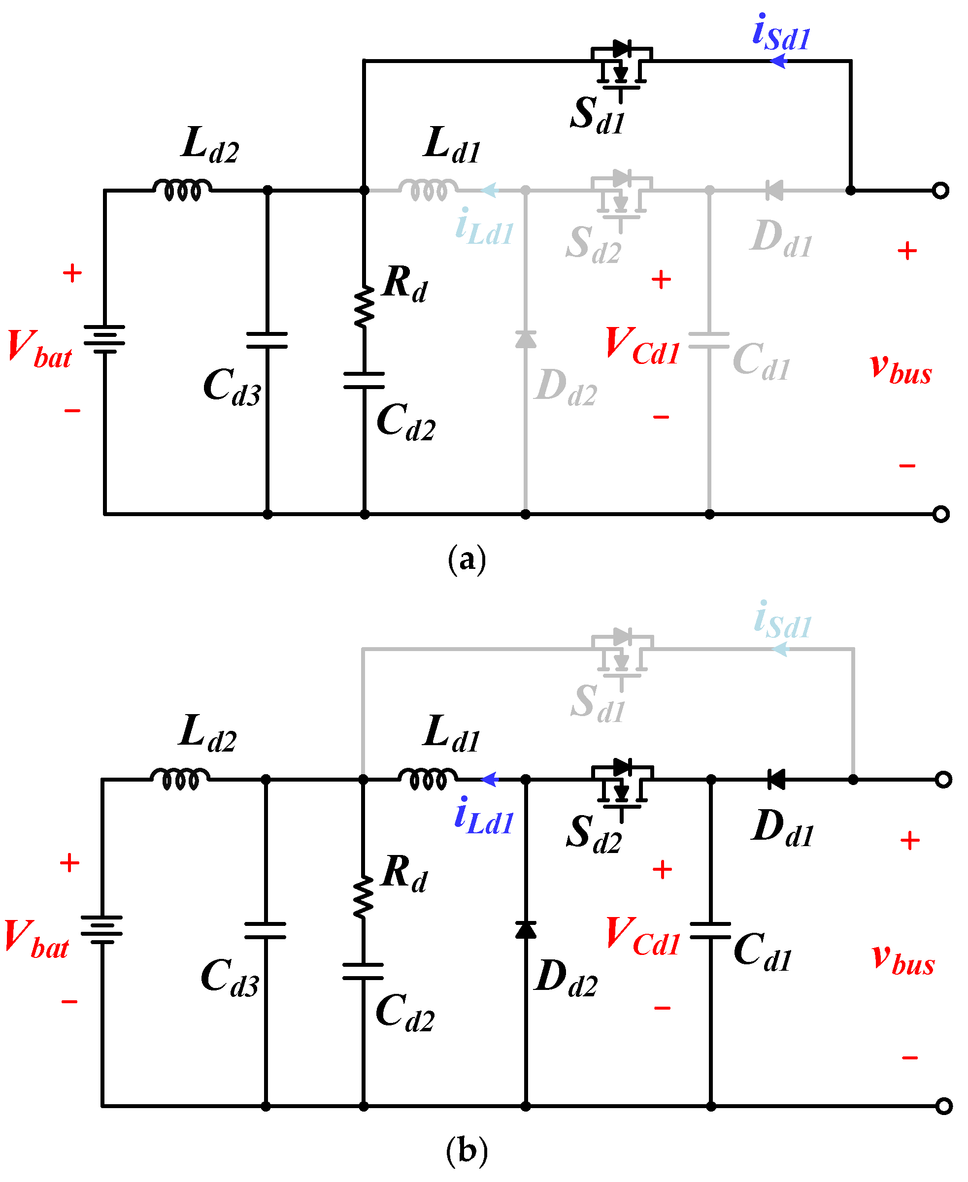
The input voltage of the DIBC has two levels: the voltage of the battery set (
Vbat) and the input voltage of the buck converter (
VCd1), depending on the operation of the selector switch
Sd1. The DIBC operates in two modes, according to the selector switch, as shown in
Figure 4.
Mode DI:
Figure 4a shows the operation of this mode,
Sd1 is turned on, and
Dd1 is turned off. The battery set is directly charged from the utility through only the CC. The input voltage of the DIBC is equal to the voltage of the battery set.
Mode DII:
Figure 4b shows the operation of this mode,
Sd1 is turned off, and
Dd1 is turned on. The battery set is charged from the utility through both the CC and buck converter. The input voltage of the DIBPC is equal to the input voltage of the buck converter, which is higher than the voltage of the battery set due to the operation of the buck converter.
The buck converter adopts a current mode control to control the current of inductor Ld1, and its operation can be divided into two modes. When Sd2 is turned on, the voltage vDd2 across Dd2 is VCd1. VCd1 is higher than the voltage of the battery set, so the current of the inductor Ld1 is increased. When SD2 is turned off, Dd2 is conducted. Consequently, the voltage vDd2 across Dd2 is 0, and the current of the inductor Ld1 is decreased. By controlling SD2 in PWM switching, the voltage vDd2 across Dd2 is a pulse voltage that varies between VCd1 and 0, which can control the current of the inductor Ld1 increasing or decreasing to follow its reference current. The reference current includes a DC component and an AC component. The DC component is used to regulate the input voltage of the buck converter. The AC component is calculated by extracting the ripple of the charging current to perform the function of DAF. Therefore, the DIBC can perform the function of DAF with no additional circuit.
5. Operation of Cascaded Converter
The CC in
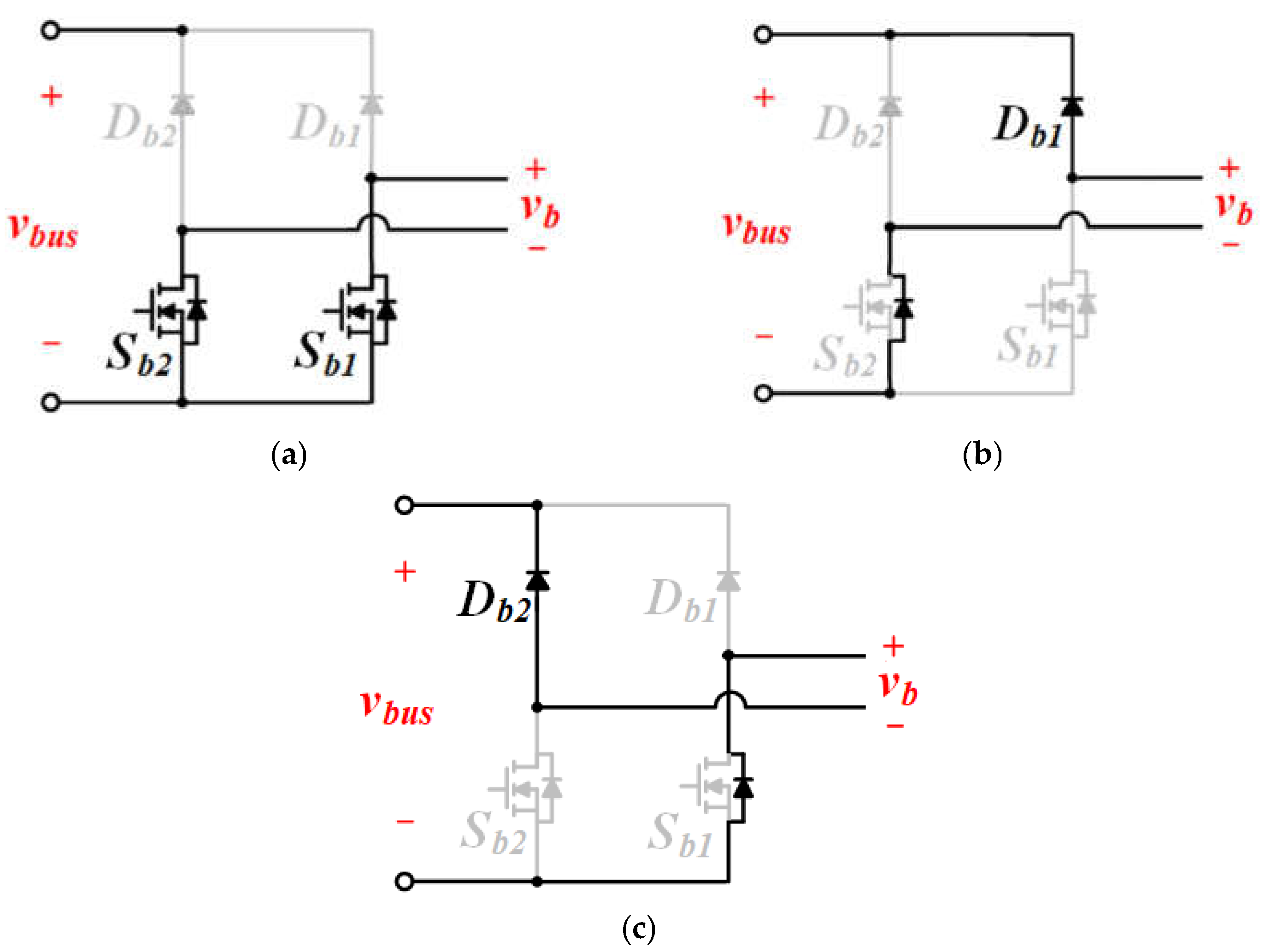
Figure 2 comprises an FBC and a BLR that are connected in series. The circuit for the BLR operates in three modes, as shown in
Figure 5.
Mode RI:
As can be seen in
Figure 5a,
Sb1, and
Sb2 are turned on, and the current path is bidirectional. The AC port voltage of the BLR is:
Mode RII:
This mode is operated during the positive half cycle of the utility voltage, as shown in
Figure 5b. The input current is positive.
Sb1 and
Sb2 are turned off, and
Db1 and the body diode of
Sb2 conduct. The AC input port voltage of the BLR is:
where
vbus is the DC port voltage of BLR.
Mode RIII:
This mode is operated during the negative half cycle of the utility voltage, as shown in
Figure 5c. The input current is negative.
Sb1 and
Sb2 are turned off, and
Db2 and the body diode of
Sb1 conduct. The AC port voltage of the BLR is:
The DC port voltage of the BLR is generated by the DIBC and has two levels: the voltage of the battery set and the input voltage of the buck converter, depending on the selector switch. The low-pass filter, configured by Cd2, Cd3, Rd, and Ld2, is used to filter out the switching ripple, and its gain is close to unity for DC voltage. As a result, the output voltage of the buck converter is almost equal to the voltage of the battery set. Sb1 and Sb2 in the BLR are switched synchronously with the utility voltage, so the BLR generates a five-level stepped voltage at the AC port. The five levels are VCd1, Vbat, 0, −Vbat, and −VCd1.
The unipolar PWM control is adopted in the FBC. The FBC generates a three-level pulse voltage at the AC port. The three levels are VCf, 0, and −VCf.
Using asymmetric voltage technology for a CC increases the number of voltage levels. Therefore, the DC port voltage of the FBC, the voltage of the battery set, and the input voltage of the buck converter are designed in the ratio of 1:2:4 to allow the CC to generate an 11-level input voltage. The operation voltage for the CC is shown in
Figure 6.
Figure 6a shows that the BLR generates a five-level step-wave voltage, which contains voltage levels of 4
VCf, 2
VCf, 0, −2
VCf, and −4
VCf.
Figure 6b shows that the FBC generates a three-level pulse voltage, where the three voltage levels are
VCf, 0, and −V
Cf. The AC port voltage of the CC integrates the AC port voltages of the FBC and the BLR to generate an 11-level pulse voltage. The voltage levels are 5
Vice, 4
VCf, 3
VCf, 2
VCf,
VCf, 0, −V
Cf, −2
VCf, −3
VCf, −4
VCf, and −5
VCf, as illustrated in
Figure 6c.
The difference in each voltage level is only
VCf, and the ripple of the input current is written as:
where
D is the duty cycle of the FBC and
fp is the frequency of the pulse voltage for the FBC. The FBC uses unipolar PWM control, so
fp is twice the switching frequency of the power electronic switches. Since the difference in each voltage level is greatly reduced, and
fp is multiplied, the filter inductor is significantly reduced in the proposed CC. Moreover, only the FBC is switched in high frequency. The DC port voltage of the FBC is about one-fifth that of a conventional PFC circuit; hence, the switching loss for the proposed CC is reduced significantly. The conduction resistance of MOSFET is proportional to its voltage rating. Hence, the conduction loss of FBC is low. Moreover, the input voltage of the buck converter is four-fifths as compared with that of the conventional PFC circuit, so the switching loss of the buck converter in the DIBC is also reduced. Although the proposed CADPCI uses a large number of components, its power efficiency is better than that of the conventional PFC circuit. In addition, the capacity of the passive filter and the EMI of the proposed CADPCI is significantly reduced as compared with the conventional PFC circuit. The DC port voltage of FBC in the proposed CC is also less than that in the asymmetrical CC with a DC port voltage ratio of 1:3, which is a quarter of the DC port voltage for the conventional PFC circuit. Therefore, the switching losses, the capacity of the passive filter, and the EMI of the proposed CC can be further reduced as compared with the asymmetrical CC with a DC port voltage ratio of 1:3.
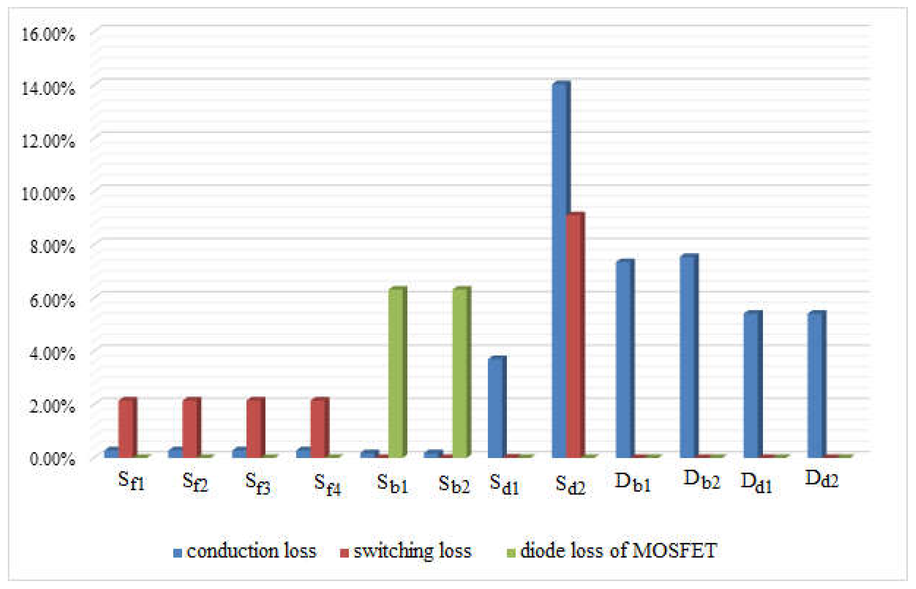
Figure 7 shows the percentage loss for the power semiconductor components in the CADPCI by using a thermal module of PSIM. For CC, the switching loss is significantly reduced. The largest loss in the CADPCI is the switching loss and conduction loss of
Sd2 of the DIBC.
The major disadvantage of CC is that the DC ports for FBCs do not have a common ground, so several independent power supplies or isolated DC-DC power converters must be used to process the DC power for the FBCs. The power balance theory is used in the proposed CC, and only a capacitor
Cf is used to be an energy buffer in the FBC, and an independent power source or an isolated DC-DC power converter is removed. The AC port voltage of the BLR (
vb) in
Figure 6b can be written as:
where
and
VAC is the amplitude of the utility voltage. The Fourier series for the AC port voltage of the BLR can be expressed as:
where
Vb0 is the average value, and it is 0.
Vbn is the amplitude of the
n-th harmonic, which is
The utility voltage is written as:
If the input current of the CC is controlled to be sinusoidal and the power factor is unity, it is written as:
The input real power for the CC is written as:
The input real power for the BLR is derived as:
The input real power for the CC is the sum of the input real powers for the BLR and the FBC, which is:
As can be seen in (13), the voltage of the battery set cannot be controlled; hence, the input real power of the BLR is controlled by the input voltage of the buck converter, VCd1. When the input real power for the BLR is rendered equal to the input real power of the CC by adjusting the input voltage of the buck converter, no real power is injected into the FBC. Therefore, an isolated DC-DC power converter is not required to convert the real power from the FBC to charge the battery set. If the DC port voltage of the FBC is less than its set value, the input voltage of the buck converter must be reduced so that the input real power for the BLR is less than that for the CC. At this time, the input real power for the FBC is positive and is used to charge the capacitor Cf. If the DC port voltage of the FBC is greater than its set value, the input voltage of the buck converter must be increased so that the input real power for the BLR is greater than that for the CC. Therefore, the input real power for the FBC has a negative value, and the capacitor Cf is discharged.
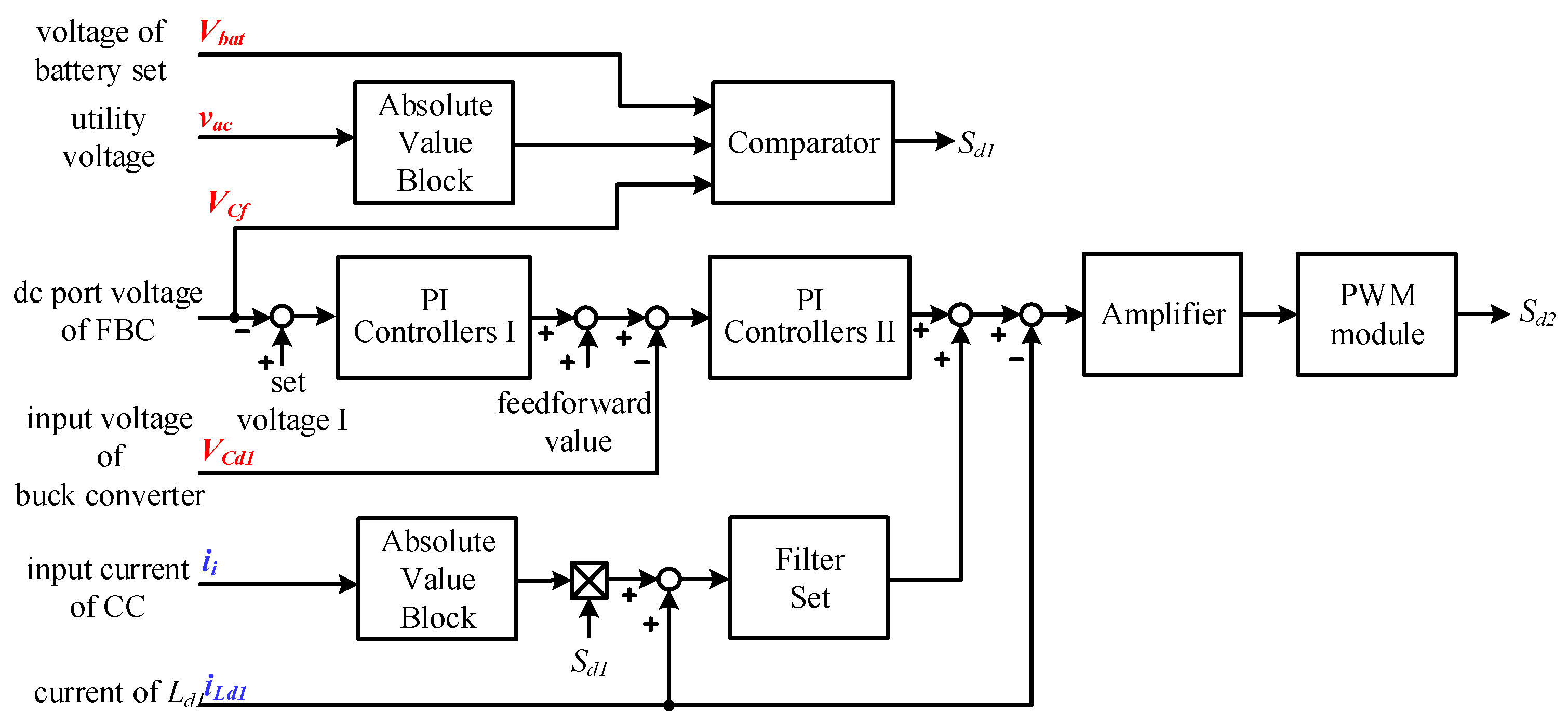
6. Control Block
Figure 8 shows the control block of the DIBC. The selector switch is controlled by comparing the absolute value of the utility voltage with the voltage of the battery set and the dc port voltage of the FBC. When the absolute value of the utility voltage is between the dc port voltage of the FBC and the input voltage of the buck converter, a control signal is generated to turn
Sd1 on.
The buck converter performs two functions. The first function is a power balance control to control the input voltage such that the input real power of the BLR is equal to the input real power of the CC. The output from the buck converter is connected to the battery set, so the output voltage of the buck converter cannot be controlled. The duty of Sd2 is used to control the input voltage. The second function is DAF, which filters out the low-frequency ripple of the charging current for the battery set by controlling the output current of the buck converter.
In order to control the power balance, the DC port voltage of FBC must be regulated. The DC port voltage of the FBC is detected and compared with the set voltage I, and then the compared result is sent to the PI controller I. A feedforward value is added to the output of PI controller I. This sum is the set value for the input voltage of the buck converter. The feedforward value is four times that of the set voltage I. The input voltage of the buck converter is detected and compared with its set value, and then the compared result is sent to PI controller II. The output of PI controller II is the power balance control signal. Because two PI controllers form a dual-loop to control the DC port voltage of the FBC and the input voltage of the buck converter, the bandwidth of two control loops must be designed to differ at least four times to avoid oscillation. Since the set value for the input voltage of the buck converter is mainly determined by the feedforward value, the PI controller I only makes fine adjustments. Therefore, the response speed of the PI controller I is designed to be slower. For controlling the input current of CC to be sinusoidal, the level voltages for the AC port of the CC should overlap slightly. Considering the fluctuation of the battery set voltage, the set voltage I is slightly higher than one-fifth of the DC port voltage of the conventional PFC circuit to ensure level voltage overlap for the AC port of the CC.
In order to realize the function of DAF, the charging current of the battery set is calculated. As seen in
Figure 2, the charging current of the battery set is the sum of the inductor current
iLd1 of the buck converter and the current
iSd1 of selection switch
Sd1. The inductor current
iLd1 is measured directly using a current detector. The current
iSd1 is calculated by multiplying the absolute value of the input current for the CC by the control signal
Sd1. The inductor current
iLd1 is added to the current
iSd1 to calculate the charging current of the battery set. The calculated charging current of the battery set is sent to a filter set to extract the low-frequency components. The filter set includes band-pass filters for 120 Hz, 240 Hz, and 360 Hz and a high-pass filter. The gains of the band-pass filters and the high-pass filter are assigned, respectively, to determine the attenuation rate for each ripple component of the charging current. Since the magnitude of the low-frequency components of the charging current is inversely proportional to their frequency, the gains for the 120 Hz, 240 Hz, and 360 Hz band-pass filter and the high-pass filter also decrease sequentially. The output of the filter set is the DAF control signal. The current reference signal is obtained by adding the power balance control signal and the DAF control signal. The current reference signal is compared with the detected inductor current iLd1, and the compared result is sent to an amplifier. The output of the amplifier is sent to a PWM module to generate the control signal of
Sd2.
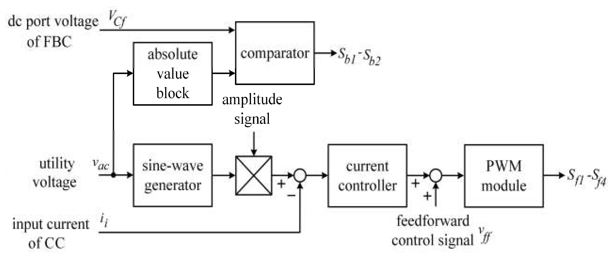
Figure 9 shows the control block of the CC. The control target of the CC is the input current. The detected utility voltage is sent to a sine-wave generator to generate a sine-wave signal with a unit amplitude that is in phase with the utility voltage. The sine-wave signal is multiplied by an amplitude signal to give the current reference signal. The amplitude signal is controlled by a constant current/constant voltage (CC/CV) charging strategy for the battery set. The battery set is charged in the CC mode, and then it is charged in the CV mode while the battery voltage reaches the floating charging voltage. The input current of the CC is detected and compared with its reference signal, and the compared result is sent to the current controller. The output of the current controller is added to a feedforward signal to give a modulation signal. The feedforward signal (
vff) is written as:
where
Vtri is the amplitude of the carrier signal for the PWM module. The modulation signal is sent to the PWM module. The PWM module uses unipolar PWM technology to generate the control signals of
Sf1–
Sf4 for the FBC. The absolute value of the utility voltage is compared with the DC port voltage of the FBC, and the compared result is used to generate the control signals for
Sb1 and
Sb2 for the BLR.
7. Experimental Results
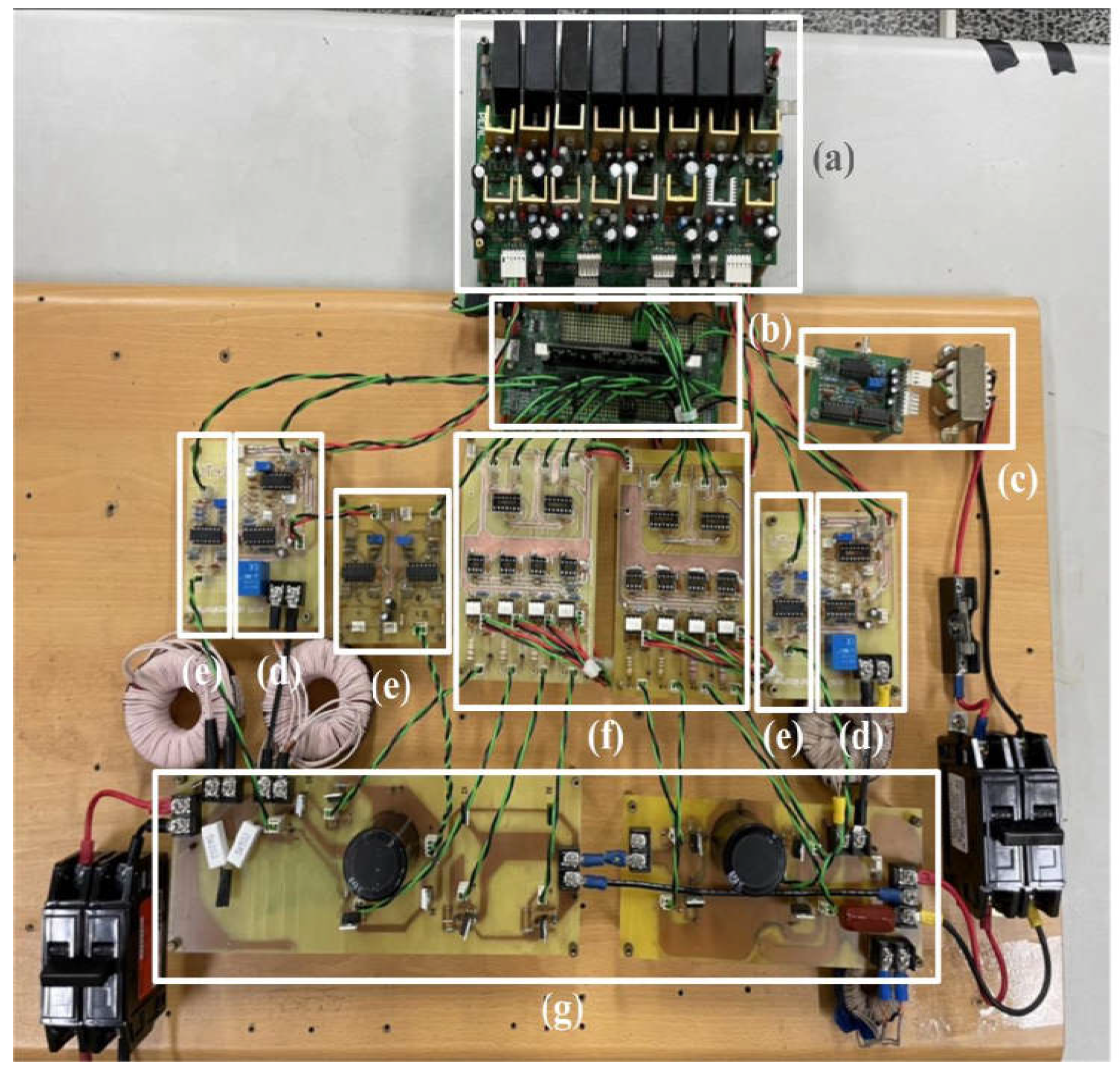
To verify the performance of the proposed CADPCI, an 800 W prototype was developed.
Figure 10 shows the photo of the prototype. The circuit parameters of the prototype are shown in
Table 1. The CADPCI is connected to a single-phase utility of 110 V and 60 Hz, and six batteries are connected in series to form the battery set. Considering the level voltage overlap for the AC port of the CC, the set voltage I for the DC port voltage of the FBC is 43 V.
Figure 11 shows the experimental results for the AC side of the CC in the steady state.
Figure 11a,b show that the AC port voltage of the CC is an 11-level voltage and is synchronized with the utility voltage.
Figure 11b,c show that the input current of the CC is a sine-wave current that is in phase with the utility voltage, so the power factor is close to unity.
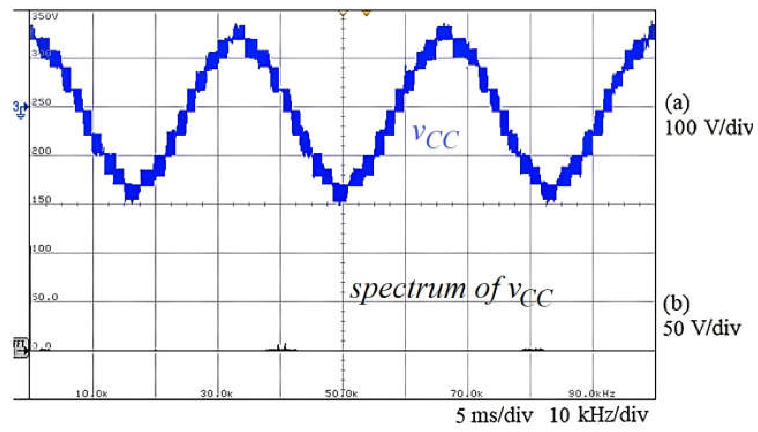
Figure 12 shows the voltage waveform and frequency spectrum for the AC port voltage of the CC. The dominant harmonics for the AC port voltage of the CC appear at around 40 kHz, which is twice the switching frequency of the FBC. The AC port voltage of the CC is an 11-level voltage, so the amplitude of the dominant harmonics is very small. Therefore, the filter inductor in the prototype is very small.
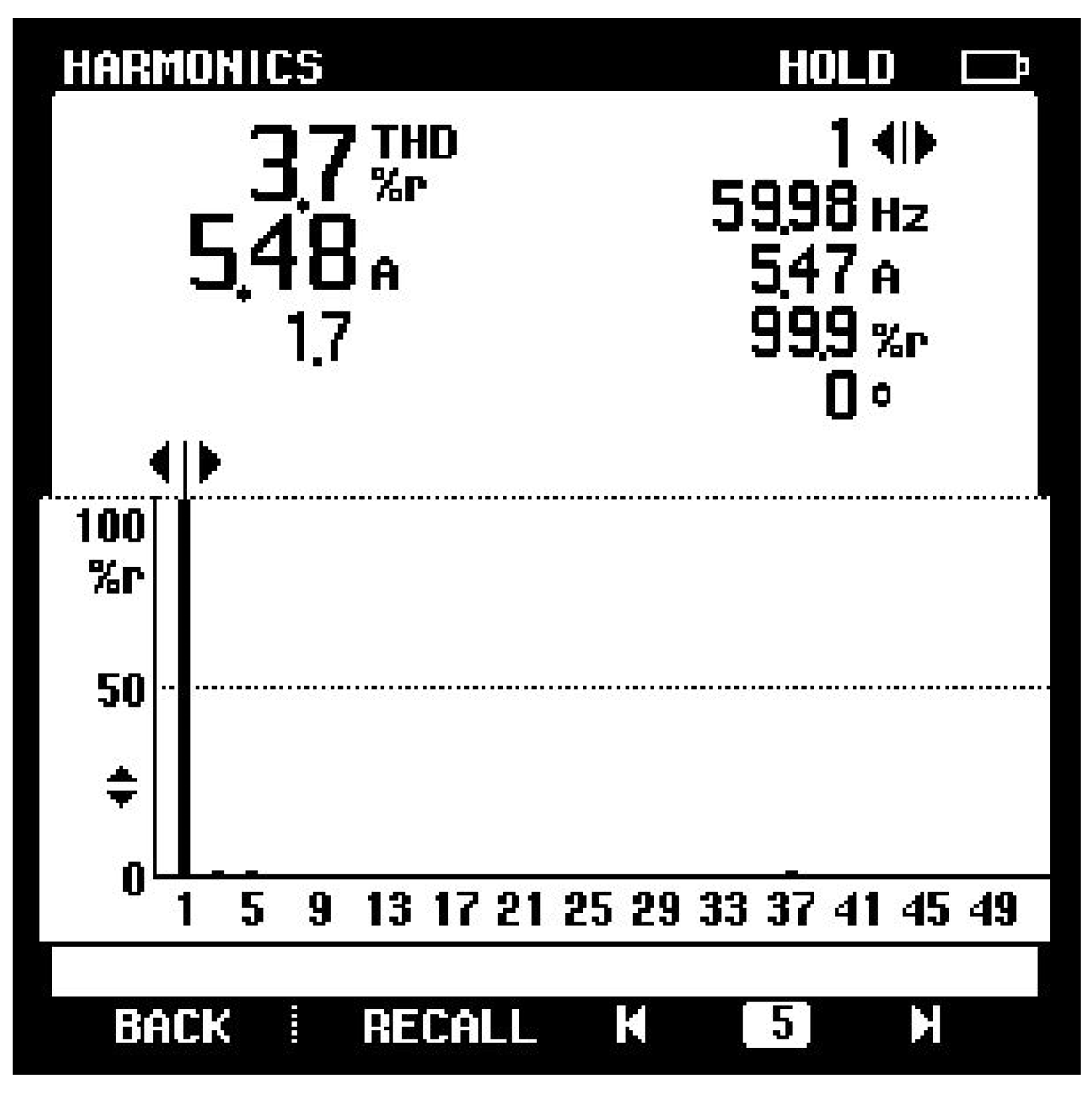
Figure 13 shows the total harmonic distortion (THD) of the input current of the CC. The THD of the input current of the CC is only 3.7%.
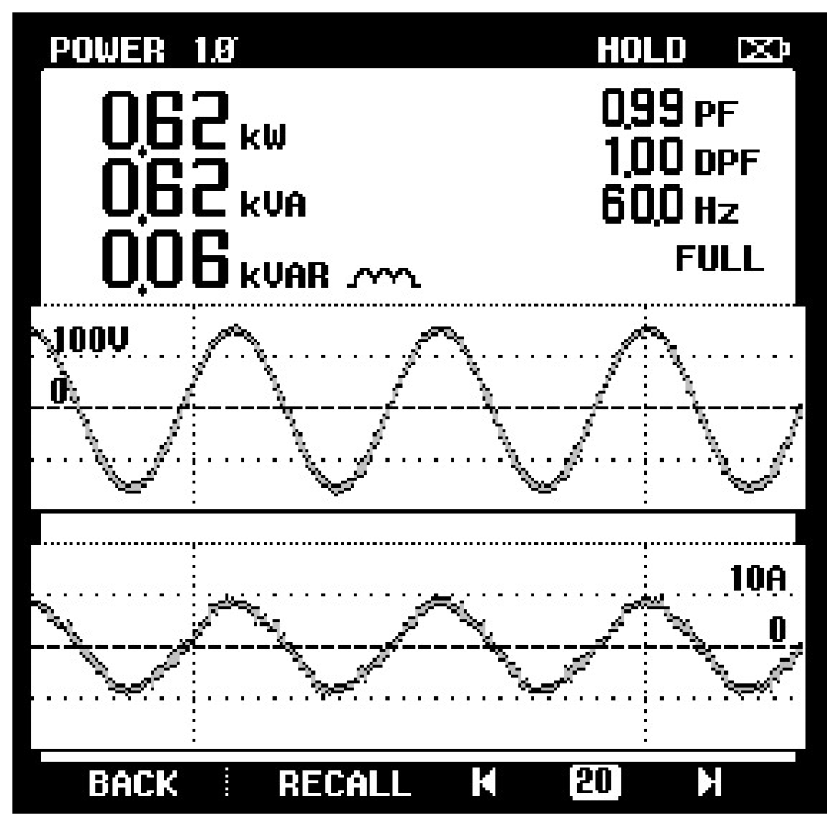
Figure 14 shows the power factor of the CC. The power factor of the CC is close to unity.
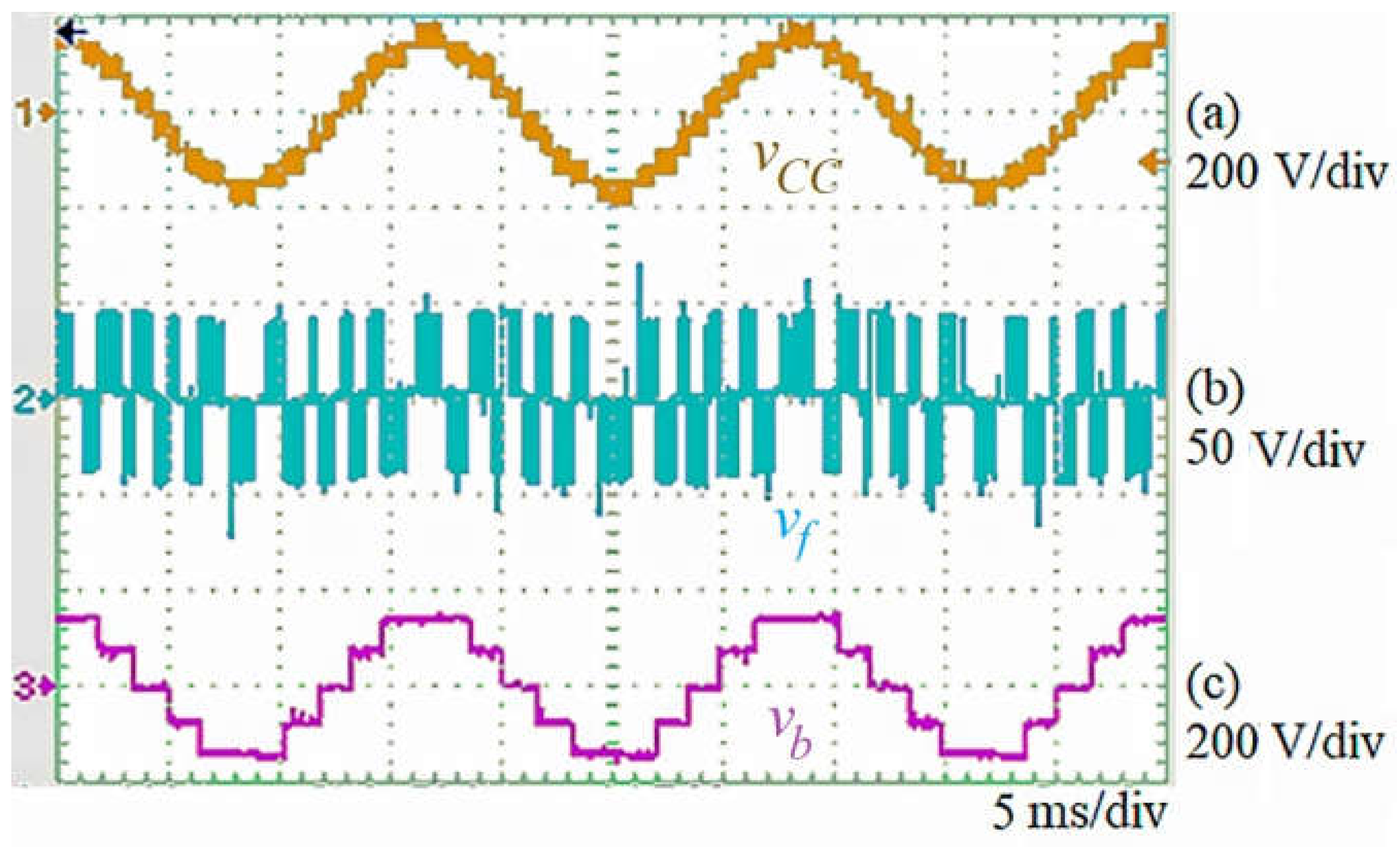
Figure 15 shows the experimental results for the voltages at the AC side of the CC.
Sb1 and
Sb2 are switched synchronously with the utility voltage, so the AC port voltage of the BDR, which is shown in
Figure 15c, is a five-level step-wave voltage. The control for the FBC uses unipolar PWM.
Figure 15b shows that the FBC generates a three-level high-frequency pulse voltage. The AC port voltage of the CC is the summation of the AC port voltages of the BLR and the FBC, so an 11-level AC voltage is generated, as shown in
Figure 15a.
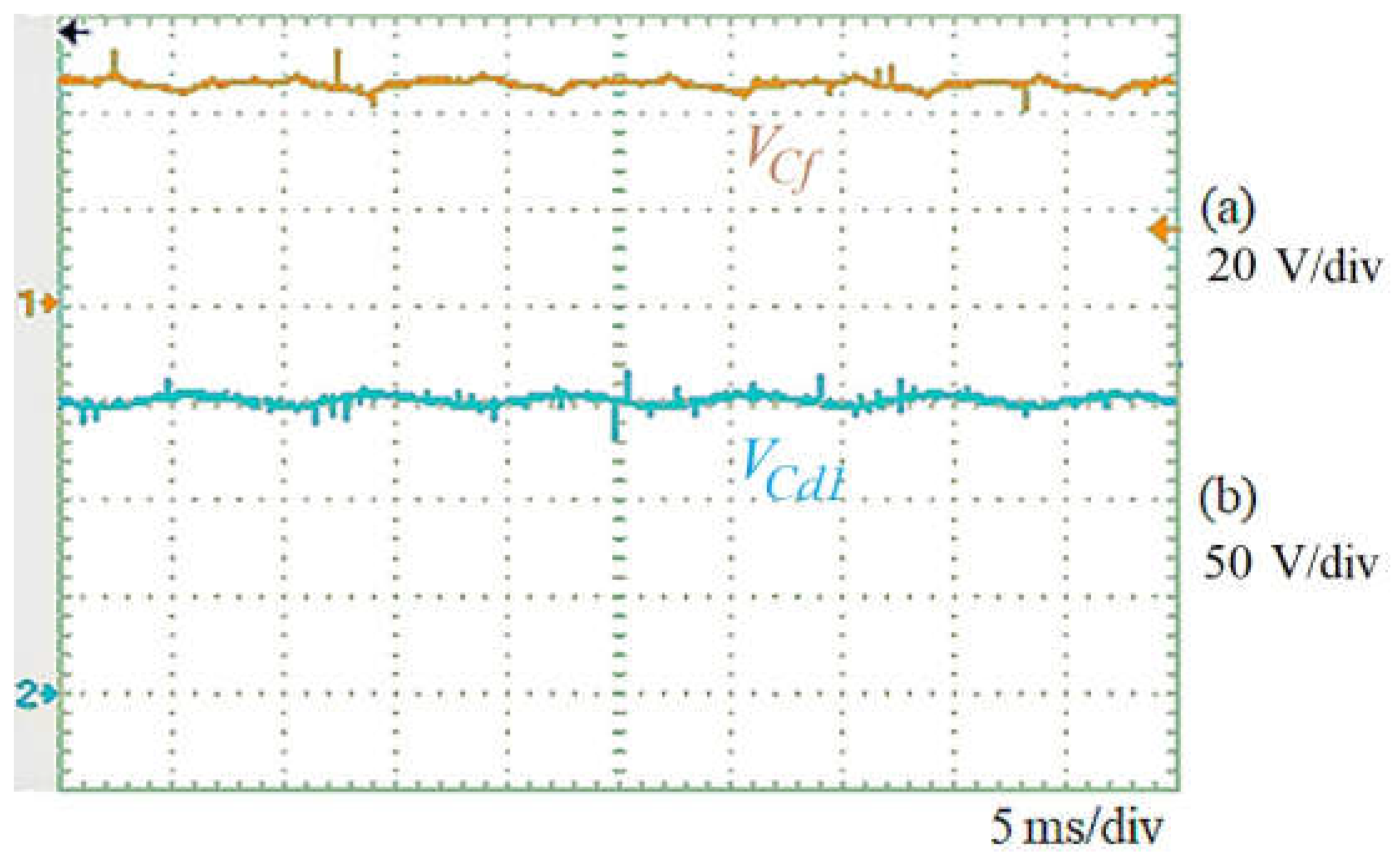
Figure 16 shows the experimental results for the DC side of the CC. The DC port voltage of the FBC is stabilized at about 43 V, and the input voltage of the buck converter is regulated at about 150 V. Therefore, it verifies that the DC port of the FBC only needs a capacitor to act as an energy buffer to stabilize the voltage, which can eliminate the need for an isolated DC-DC power converter.
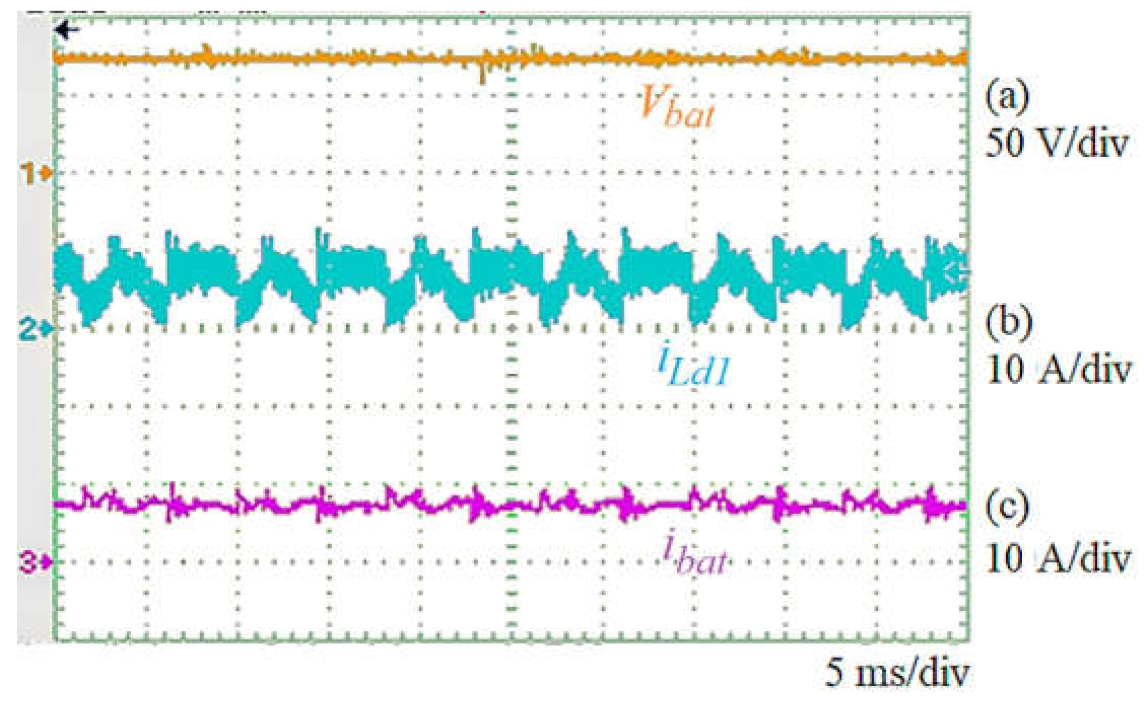
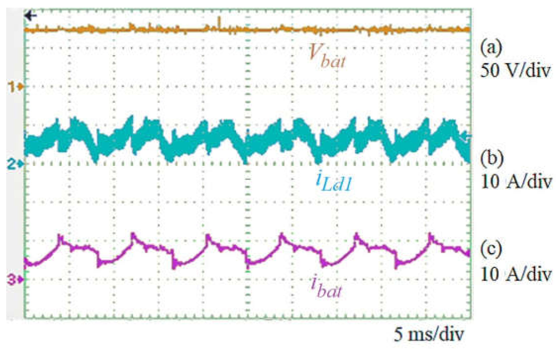
Figure 17 and
Figure 18 show the experimental results for the DIBC with and without the function of DAF. As can be seen in
Figure 17c and
Figure 18c, it verifies that the DIBC, with the function of DAF, can effectively suppress the low-frequency ripple of the charging current for the battery set.
Figure 19 shows the power efficiency of the CADPCI under the different output voltages. The higher the input voltage is, the higher the power efficiency will be. The maximum power efficiency of CADPCI is 96.68%.
According to the experimental results, the merits of the prototype are summarized in
Table 2.
8. Conclusions
An AC-DC power conversion interface with a stable and controllable DC voltage/current and unity power factor correction is expected to improve the power quality of electronic equipment and the performance of a battery set. A CADPCI is proposed to convert AC power from the utility into stable DC power to charge a battery set.
The experimental results show that the CC generates an 11-level voltage at the AC port and performs unity power factor correction. The dominant harmonics of the AC port voltage for the CC occur at around 40 kHz, and the amplitude is very small due to eleven voltage levels. The DC port of the FBC only needs a capacitor to stabilize the voltage, so there is no need for an isolated DC-DC power converter. The DIBC can effectively suppress the low-frequency ripple of the charging current for the battery set.
The proposed CADPCI has the advantages of higher power efficiency, the lower capacity of the passive filter, and the EMI. Hence, the proposed CADPCI is suitable for charging the battery of electric vehicles, robots, and home-based battery energy storage systems.


