
A Novel 8T XNOR-SRAM: Computing-in-Memory Design for Binary/Ternary Deep Neural Networks


Abstract
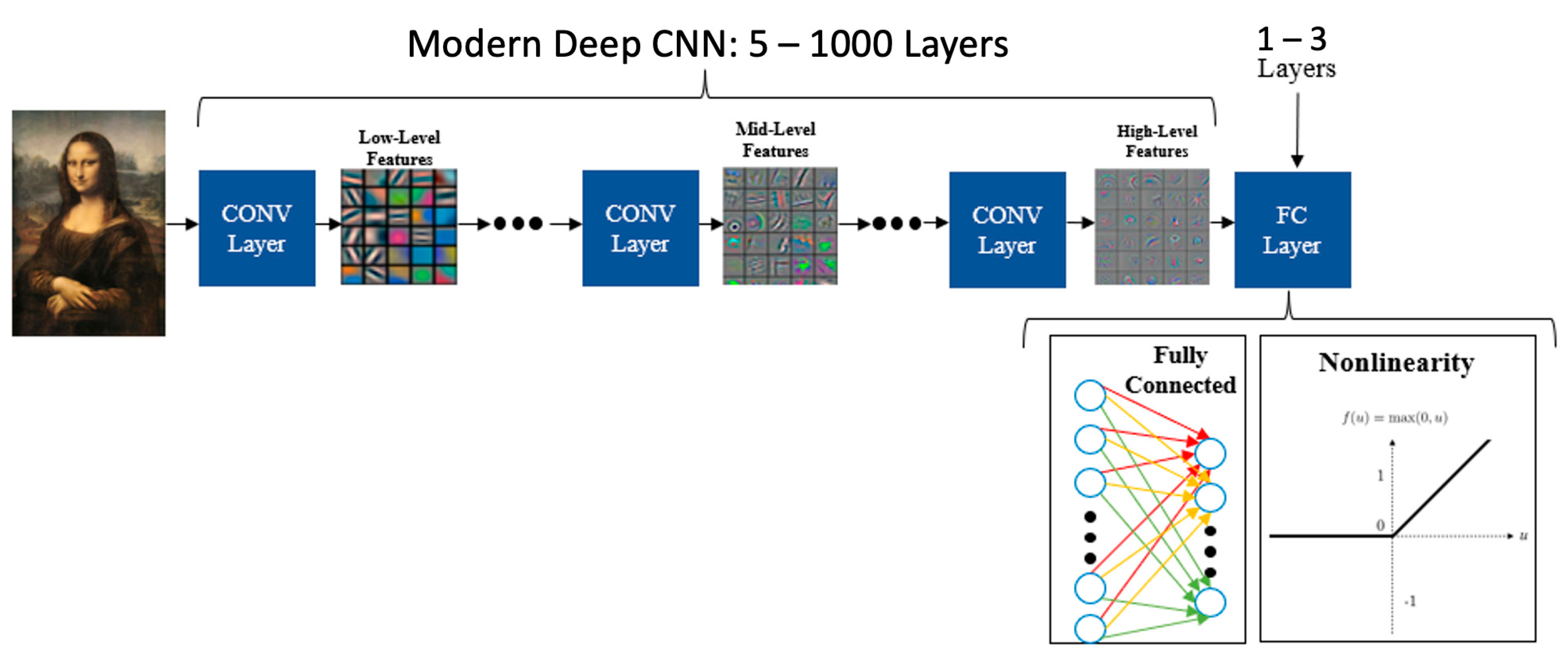
:1. Introduction
2. Trends and Challenges of SRAM-CIM for AI Applications
2.1. Principle of CIM
2.2. Challenges of SRAM-CIM
2.3. SRAM-CIM Designs
3. Proposed XNOR-SRAM Design and Optimization
3.1. XNOR-SRAM Bitcell Design
3.2. Proposed CIM Operation and Analysis
- Binary Weights and Binary Activations: For binary activations, the bit cell produces the XNOR dot-product output of (+1) once, with one strong PU by NMOS, and once with one strong PU by PMOS in two ways. The first is when the input is (+1), and the weight is (+1), and the second is when the input is (−1) and the weight is (−1), respectively. Firstly, the (XN) and (XP) inputs are high at VDD, and the weight stored in the Q node is also high at VDD. So, the XNOR dot-product output is generated by turning the NMOS transistor ON and, thus, driving the (XL) high to (VDD-Vth) via the Q node. Secondly, the (XN) and (XP) inputs are low at 0, and the weight stored in the Q node is also low at 0. So, the XNOR dot-product output is generated by turning the PMOS transistor ON and, thus, driving the (XL) high to (VDD-Vth) via the QB node. The bit cell produces the XNOR dot-product output of (−1) once with one strong PU by NMOS and once with a one strong PU by PMOS in two ways. The first is when the input is (+1), and the weight is (−1), and the second when the input is (−1), and the weight is (+1), respectively. Firstly, the (XN) and (XP) inputs are high at VDD, and the weight stored in the Q node is low at 0. So, the XNOR dot-product output is generated by turning the NMOS transistor ON, and thereby driving the voltage of (XL) to discharge. Secondly, the (XN) and (XP) inputs are low at 0, and the weight stored in the Q node is high at 1. So, the XNOR dot-product output is generated by turning the PMOS transistor ON, and thereby the voltage of (XL) is discharged via the QB node. This is described in rows 1–4 in Table 2, and shown in the first two rows in Figure 3b. From Table 2, it is shown that we represented the weight (+1) with (Q = VDD & Qb = 0) and we represented the Weight (−1) with (Q = 0 & Qb = VDD). For the input (+1) (XN & XP = VDD) and the input (−1) (XN & XP = 0). We presented the input (0) in two ways, either (XN = 0 & XP = VDD) or (XN = VDD & XP = 0).
- Binary Weights and Ternary Activations: To exhibit the ternary activations, we had to consider the input (activation) value of (0). For ternary activations, the bit cell produces the XNOR dot-product output of (0) in two ways. First, when the input is (0), and the weight is (+1), and second, when the activation is (0), and the weight is (−1). Now taking into consideration that the XNOR-output (0) did not contribute to the voltage of the XNOR line (XL), we still had to present it and perform the calculation of it. There are two ways to produce the XNOR dot-product output of (0). In the first method, we turned both transistors OFF by setting the inputs (XN) low at 0 and (XP) high at VDD, and we named this (0-even-rows). In the second method, we turned both transistors ON, and this was done to consider when the input combination of (XN) was high at VDD and (XP) low at 0, and we named this (0-odd-rows). We also assumed that the XNOR mode driver would distribute the input combinations of the XNOR (0) on the 255 rows evenly. This is described in rows 5–8 in Table 2, and shown in the last two rows in the Figure 3b.
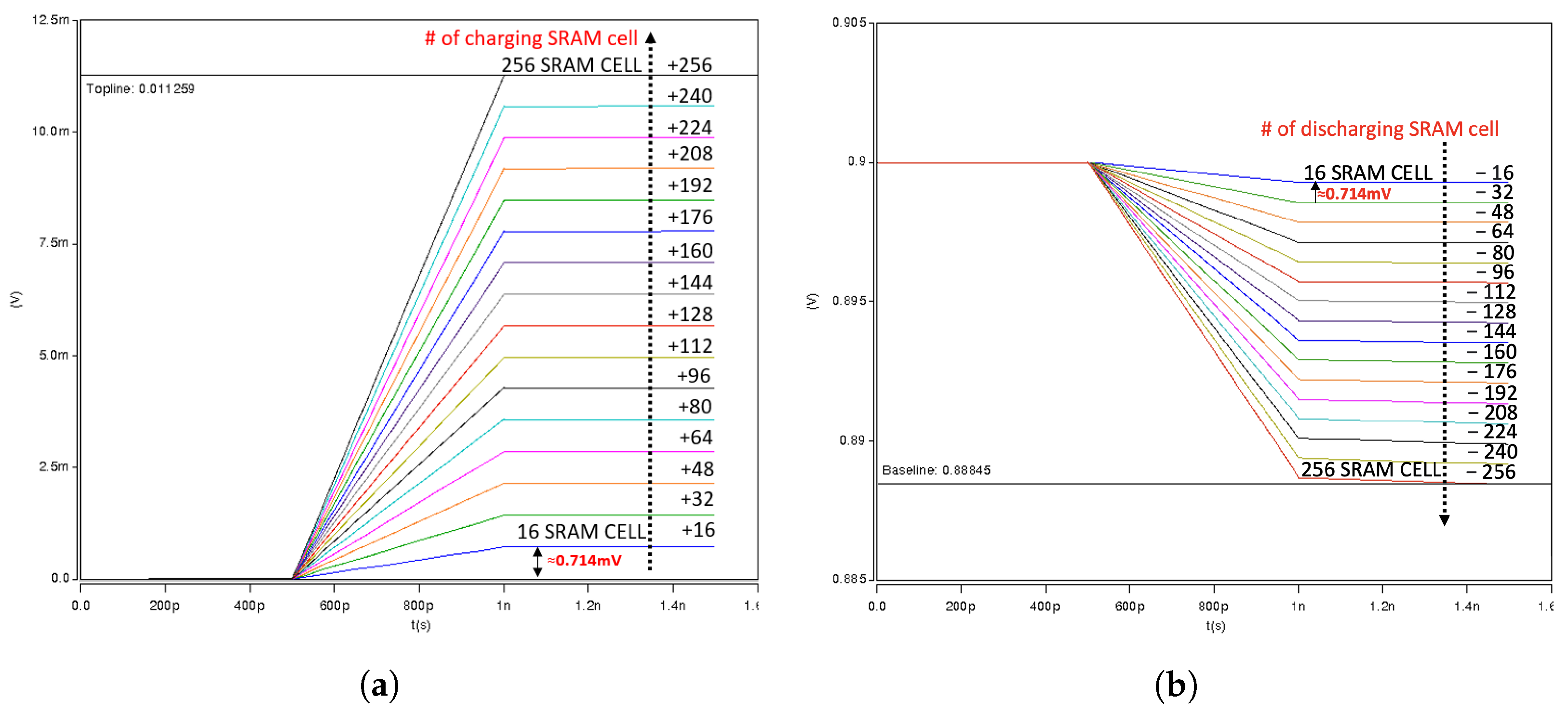
- ADC Operation Description: As stated earlier, the design consisted of 256-bit cells in one column, and 64 cells for the dot-product operations. The ADC block in the design consisted of 32 cells for ADC reference and 32 cells for ADC calibration. The dot-product analog result obtained from the XL was quantized using a comparator ADC. We quantized our analog summation of the dot-product results using Equation (1) below, where N is the number of output bits. Thus, we needed 33 cycles for ADC. In 33 cycles for the ADC operation, where each cycle was an ADC reference, the cell values could be swept from (−32 to +32) for a step size of 2. The dot-product results were compared to the comparator ADC primary operation method as if the dot-product was less than the ADC reference value, it was quantized to 0, and if it was equal to, or larger than, the ADC reference value, it was quantized to 1.
4. Measurement Results
5. Conclusions
Author Contributions
Funding
Acknowledgments
Conflicts of Interest
Abbreviations
| SRAM | Static Random-Access Memory |
| eNVM | Embedded-non-Volatile-Memory |
| CIM | Compute-In-Memory |
| ADC | Analog to Digital Converter |
| TBN | Ternary Binary Neural Networks |
| MAC | Multiply-And-Accumulate |
| VMM | Vector-Matrix Multiplication |
| GPU | Graphical Processing Unit |
| TPU | Tensor Processing Unit |
| SET | Single-event Transient |
| DNU | Double-node Upset |
References
- Hinton, G.; Deng, L.; Yu, D.; Dahl, G.E.; Mohamed, A.-R.; Jaitly, N.; Senior, A.; Vanhoucke, V.; Nguyen, P.; Sainath, T.N.; et al. Deep neural networks for acoustic modeling in speech recognition: The shared views of four research groups. IEEE Signal Process. Mag. 2012, 29, 82–97. [Google Scholar] [CrossRef]
- Taigman, Y.; Yang, M.; Ranzato, M.A.; Wolf, L. DeepFace: Closing the gap to human-level performance in face verification. In Proceedings of the IEEE Conference on Computer Vision and Pattern Recognition, Columbus, OH, USA, 24–27 June 2014; pp. 1701–1708. [Google Scholar]
- Fang, W.; Wang, L.; Ren, P. Tinier-YOLO: A Real-Time Object Detection Method for Constrained Environments. IEEE Access 2020, 8, 1935–1944. [Google Scholar] [CrossRef]
- Sze, V.; Chen, Y.-H.; Yang, T.-J.; Emer, J.S. Efficient Processing of Deep Neural Networks: A Tutorial and Survey. Proc. IEEE 2017, 105, 2295–2329. [Google Scholar] [CrossRef]
- Chan, T.-H.; Jia, K.; Gao, S.; Lu, J.; Zeng, Z.; Ma, Y. PCANet: A Simple Deep Learning Baseline for Image Classification? IEEE Trans. Image Process. 2015, 24, 5017–5032. [Google Scholar] [CrossRef] [PubMed]
- Abdel-Hamid, O.; Mohamed, A.-R.; Jiang, H.; Deng, L.; Penn, G.; Yu, D. Convolutional Neural Networks for Speech Recognition. Proc. IEEE/ACM Trans. Audio Speech Lang. Process. 2014, 22, 1533–1545. [Google Scholar] [CrossRef]
- Rastegari, M.; Ordonez, V.; Redmon, J.; Farhadi, A. XNOR-Net: ImageNet classification using binary convolutional neural networks. In European Conference on Computer Vision; Springer International Publishing: Cham, Switzerland, 2016. [Google Scholar]
- Wan, D.; Shen, F.; Liu, L.; Zhu, F.; Qin, J.; Shao, L.; Shen, H.T. TBN: Convolutional Neural Network with Ternary Inputs and Binary Weights. In Proceedings of the European Conference on Computer Vision (ECCV), Munich, Germany, 8–14 September 2018. [Google Scholar]
- Song, T.; Jung, J.; Rim, W.; Kim, H.; Kim, Y.; Park, C.; Do, J.; Park, S.; Cho, S.; Jung, H.; et al. A 7nm FinFET SRAM using EUV lithography with dual writedriver-assist circuitry for low-voltage applications. In Proceedings of the IEEE International SolidState Circuits Conference (ISSCC), San Francisco, CA, USA, 11–15 February 2018. [Google Scholar]
- Yu, S.; Jiang, H.; Huang, S.; Peng, X.; Lu, A. Compute-in-Memory Chips for Deep Learning: Recent Trends and Prospects. IEEE Circuits Syst. Mag. 2021, 21, 31–56. [Google Scholar] [CrossRef]
- Yan, A.; Zhou, J.; Hu, Y.; Cui, J.; Huang, Z.; Girard, P.; Wen, X. Novel Quadruple Cross-Coupled Memory Cell Designs with Protection Against Single Event Upsets and Double-Node Upsets. IEEE Access 2019, 7, 176188–176196. [Google Scholar] [CrossRef]
- Lu, A.; Peng, X.; Luo, Y.; Yu, S. Benchmark of the compute-inmemory based DNN accelerator with area constraint. IEEE Trans. VLSI Syst. 2020, 28, 1945–1952. [Google Scholar] [CrossRef]
- Si, X.; Khwa, W.-S.; Chen, J.-J.; Li, J.-F.; Sun, X.; Liu, R.; Yu, S.; Yamauchi, H.; Li, Q.; Chang, M.-F. A Dual-Split 6T SRAM-Based Computing-in-Memory Unit-Macro With Fully Parallel Product-Sum Operation for Binarized DNN Edge Processors. IEEE Trans. Circuits Syst. I Regul. Pap. 2019, 66, 4172–4185. [Google Scholar] [CrossRef]
- Yin, S.; Jiang, Z.; Seo, J.-S.; Seok, M. XNOR-SRAM: In-Memory Computing SRAM Macro for Binary/Ternary Deep Neural Networks. IEEE J. Solid State Circuits 2020, 55, 1733–1743. [Google Scholar] [CrossRef]
- Biswas, A.; Chandrakasan, A.P. CONV-SRAM: An Energy-Efficient SRAM With In-Memory Dot-Product Computation for Low-Power Convolutional Neural Networks. IEEE J. Solid State Circuits 2019, 54, 217–230. [Google Scholar] [CrossRef] [Green Version]


| No. | Transistors | Ratio | Size of Transistors |
|---|---|---|---|
| 1 | T1 | 8 | m |
| 2 | T2 | 1 | m |
| 3 | T3 | 8 | m |
| 4 | T4 | 1 | m |
| 5 | T5 | 4 | m |
| 6 | T6 | 4 | m |
| 7 | T7 | 1 | m |
| 8 | T8 | 1 | m |
| XNOR Operation | |||||||
|---|---|---|---|---|---|---|---|
| Row | Operation | Inputs | Weights | Output | |||
| Input | Weight | XN | XP | Q | QB | XL | |
| 1 | +1 | +1 | VDD | VDD | VDD | 0 | +1 |
| 2 | +1 | −1 | VDD | VDD | 0 | VDD | −1 |
| 3 | −1 | +1 | 0 | 0 | VDD | 0 | −1 |
| 4 | −1 | −1 | 0 | 0 | 0 | VDD | +1 |
| 5 EVEN | 0 | +1 | 0 | VDD | VDD | 0 | 0 |
| 6 EVEN | 0 | +1 | 0 | VDD | 0 | VDD | 0 |
| 7 ODD | 0 | −1 | VDD | 0 | VDD | 0 | 0 |
| 8 ODD | 0 | −1 | VDD | 0 | 0 | VDD | 0 |
| Operation | Power Consumption (W) | |||
|---|---|---|---|---|
| Input | Weight | State-of-the-Art [14] | Proposed CIM | Improvement |
| +1 | +1 | 30% | ||
| +1 | −1 | 52% | ||
| −1 | +1 | 59% | ||
| −1 | −1 | 35% | ||
| 0 | +1 | 98% | ||
| 0 | −1 | 97% | ||
| 0 | +1 | 88% | ||
| 0 | −1 | 42% | ||
| Operation | Delay (s) | |||
|---|---|---|---|---|
| Input | Weight | State-of-the-Art [14] | Proposed CIM | Improvement |
| +1 | +1 | 30% | ||
| +1 | −1 | 50% | ||
| −1 | +1 | 90% | ||
| −1 | −1 | 88% | ||
Disclaimer/Publisher’s Note: The statements, opinions and data contained in all publications are solely those of the individual author(s) and contributor(s) and not of MDPI and/or the editor(s). MDPI and/or the editor(s) disclaim responsibility for any injury to people or property resulting from any ideas, methods, instructions or products referred to in the content. |
© 2023 by the authors. Licensee MDPI, Basel, Switzerland. This article is an open access article distributed under the terms and conditions of the Creative Commons Attribution (CC BY) license (https://creativecommons.org/licenses/by/4.0/).
Share and Cite
Alnatsheh, N.; Kim, Y.; Cho, J.; Choi, K.K. A Novel 8T XNOR-SRAM: Computing-in-Memory Design for Binary/Ternary Deep Neural Networks. Electronics 2023, 12, 877. https://doi.org/10.3390/electronics12040877
Alnatsheh N, Kim Y, Cho J, Choi KK. A Novel 8T XNOR-SRAM: Computing-in-Memory Design for Binary/Ternary Deep Neural Networks. Electronics. 2023; 12(4):877. https://doi.org/10.3390/electronics12040877
Chicago/Turabian StyleAlnatsheh, Nader, Youngbae Kim, Jaeik Cho, and Kyuwon Ken Choi. 2023. "A Novel 8T XNOR-SRAM: Computing-in-Memory Design for Binary/Ternary Deep Neural Networks" Electronics 12, no. 4: 877. https://doi.org/10.3390/electronics12040877