Article

A Methodology for Accelerating FPGA Fault Injection Campaign Using ICAP

by
Frederico Ferlini
1,
Felipe Viel
2,
Laio Oriel Seman
3,*,
Hector Pettenghi
2,
Eduardo Augusto Bezerra
2 and
Valderi Reis Quietinho Leithardt
4,5
1
System & Verification Group, Cadence Design Systems GmbH, 85622 Feldkirchen, Germany
2
Department of Electrical Engineering, Federal University of Santa Catarina (UFSC), Florianópolis 88040-900, Brazil
3
Graduate Program in Applied Computer Science, University of Vale do Itajaí (UNIVALI), Itajaí 88302-901, Brazil
4
COPELABS—Lusófona University of Humanities and Technologies, Campo Grande 376, 1749-024 Lisboa, Portugal
5
VALORIZA, Research Center for Endogenous Resources Valorization, Instituto Politécnico de Portalegre, 7300-555 Portalegre, Portugal
*
Author to whom correspondence should be addressed.
Electronics 2023, 12(4), 807; https://doi.org/10.3390/electronics12040807
Submission received: 26 December 2022 / Revised: 1 February 2023 / Accepted: 2 February 2023 / Published: 6 February 2023
(This article belongs to the Special Issue FPGAs Based Hardware Design)

Abstract

:
The increasing complexity of System-on-Chip (SoC) and the ongoing technology miniaturization on Integrated Circuit (IC) manufacturing processes makes modern SoCs more susceptible to Single-Event Effects (SEE) caused by radiation, even at sea level. To provide realistic estimates at a low cost, efficient analysis techniques capable of replicating SEEs are required. Among these methods, fault injection through emulation using Field-Programmable Gate Array (FPGA) enables campaigns to be run on a Circuit Under Test (CUT). This paper investigates the use of an FPGA architecture to speed up the execution of fault campaigns. As a result, a new methodology for mapping the CUT occupation on the FPGA is proposed, significantly reducing the total number of faults to be injected. In addition, a fault injection technique/flow is proposed to demonstrate the benefits of cutting-edge approaches. The presented technique emulates Single-Event Transient (SET) in all combinatorial elements of the CUT using the Internal Configuration Access Port (ICAP) of Xilinx FPGAs.

1. Introduction

In recent years, the constant advances in Integrated Circuit (IC) manufacturing technology, such as shrinking, high package density, and low operating voltage, have led to increased radiation susceptibility. This is no longer just a concern for space applications, as even commercially used nanoscale circuits at sea level have become more susceptible to particles present in the atmosphere [1,2,3,4]. The widespread presence of ICs in various fields, including aerospace, military, medical systems, and even household appliances, such as Internet of Things (IoT) systems, makes fault-tolerant techniques increasingly important for space and terrestrial applications [5,6,7]. Finding efficient methods for evaluating these techniques to meet this demand is essential. It is crucial to enable this evaluation early in the IC design process in order to minimize the budget spent on expensive particle accelerator facilities [5,6,7,8].
Hardware fault injection is widely accepted to evaluate the response of a circuit in the presence of faults. Thus, it plays a key role in validating fault tolerance techniques applied during the design of robust circuits [9,10].
Physical fault injection using accelerated particle radiation or laser beams, as well as simulation- and emulation-based approaches, are examples of related work in fault injection. Due to the high cost and requirement of a prototype, physical injection produces realistic results but is limited to circuit characterization and is unsuitable for early design stages. Simulation-based approaches allow for early verification of a response of a circuit. However, they require a lot of computing power and can be prohibitively time-consuming for complex designs. Emulation-based approaches, such as those based on Field-Programmable Gate Arrays (FPGAs), allow for faster fault injection execution and early design stage evaluation. However, many of these approaches necessitate hardware model modification, which can be intrusive and limit their applicability [11,12,13].
The main contribution of this paper is a new Fault Injection Based on Emulation (FIBEM) that reduces the total number of faults injected while improving execution time and fault coverage results. The method employs a FPGA as a case study and is based on the dynamic partial reconfiguration of FPGA. The proposed flow is described in detail in the paper, as is the developed framework. The approach’s effectiveness is demonstrated through case studies using a Xilinx FPGA.
The related work is discussed in Section 2. Section 3 investigates the FPGA architecture to define the new fault injection approach. Section 4 presents the proposed fault emulation flow. Section 5 evaluates the proposed approach in two case studies. Future research and closing remarks are in Section 6.

2. Related Work

The exposition to radiation can cause permanent errors (hard errors) and transient errors (soft errors). The physical phenomenon of particle interaction with the silicon material is vastly complex and requires specific mathematical and statistical models. A full-chip simulation cannot afford to use these complex models due to its prohibitive computation time [11,14]. On the other hand, digital circuits present a common behavior whenever a radiation event occurs, and its effect at a logical level can be modeled. For instance, a bit-flip behavior caused by radiation can be modeled as a Single-Event Effect (SEE), which can be reproduced through fault injection to analyze larger digital designs [2,3,4,11,15].
While the hardness of commercial ICs has generally improved considering hard errors, the technological changes resulted in more susceptibility to transient radiation effects, thus requiring more attention to faults caused by SEE [16]. Among SEEs, we can distinguish Single-Event Transient (SET) that model the transitory variation of a combinatory output and Single-Event Upset (SEU) that represents the toggle (or bit-flip) of a memory element state when a SEE occurs [6,11,16].
There are several forms of fault injections, each one of them with advantages and limitations. Physical fault injection using accelerated particle radiation or laser beam produces realistic results without sending the IC to the space environment. However, few facilities have the equipment to support this kind of injection, and they are mainly used to characterize the radiation tolerance of circuits due to their high cost [1,11,17,18,19].
The authors of [20] also employed physical injection to mimic fault effects by “pin forcing” the IC Input/Output (I/O) interface. This technique does not apply to the complex circuit designs of today since it is restricted to IC boundaries. Moreover, a prototype is required to inject faults physically, thus impeding the execution of fault campaigns early in the design.
Fault injection techniques using IC abstract models allow the verification of a circuit’s response and expose its soft spots when faults occur. For instance, the authors of [21] use a LEON3 model described in SystemC transaction level for the fault injection. Mutants are added to the model to simulate the fault effect in the memory sections (stack, instruction, data, etc.) of the LEON3 processor. The tool MEFISTO [22] uses a simulator’s saboteurs, mutants, and specific commands to more accurately replicate the fault effects in models described in VHSIC Hardware Description Language (VHDL).
The simulation-based fault injection allows the circuit analysis early in the project. However, it requires significant computing resources to perform the fault injection, and its execution time can become prohibitive for complex designs. Fault emulation addresses this challenge and uses FPGAs instead of a simulation tool to accelerate the fault injection execution. There is an autonomous technique to analyze the effect of SEUs [23] and SETs [24] using instrumentation (modification of the hardware model to support the fault emulation). In the same way, ref. [25] adds hardware to the model of the Circuit Under Test (CUT) in order to inject SEU faults and analyze the circuit behavior. Those techniques drastically reduce the execution time through emulation-based fault injection compared to simulation. However, it is an intrusive approach, as the instrumentation requires modifying the hardware model.
The partial reconfiguration feature available in some FPGAs allows fault injection without modifying the hardware description of the CUT model. FLIPPER [26] uses Xilinx FPGAs to verify CUT susceptibility to the effects of SEUs through the collection of the probability distribution of the number of faults required to cause a functional failure. A host computer controls the fault injection in FLIPPER, and it has access to the configuration memory of the FPGA that contains the implementation of the CUT. The host manipulates the configuration memory passing through all bits to identify which are susceptible (affecting the normal behavior of the CUT). The results obtained by FLIPPER are compared and validated against those generated by a particle accelerator [27], showing the applicability of fault emulation.
The FT-UNSHADES [28] uses a system control partially implemented in the FPGA to optimize the fault injection campaign injection, removing the communication bottleneck between the host and the FPGA. The FT-UNSHADES uses a Xilinx FPGA to implement the emulation controller with two copies of the CUT, in which only the FAULTY instance is fault injected. The GOLDEN (fault-free) version is a reference for the output comparison of both CUT instances.
An embedded softcore processor is used in [29] to control the fault injection. In this approach, the Xilinx FPGAs ICAP feature is used to inject the fault via dynamic partial reconfiguration of the FPGA configuration memory. Following the same idea, ref. [30] uses the Xilinx MicroBlaze microprocessor in a Virtex5 FPGA to control the Internal Configuration Access Port (ICAP) and to perform the fault injection of the CUT. However, these fault emulation techniques sweep all the FPGA configuration memory bits to inject faults randomly, regardless of the exact location of the CUT implementation. This approach continually tests the whole FPGA device despite the CUT implementation, thus affecting the execution time due to the significant number of faults to be injected. Furthermore, the manufacturer often indicates how to perform such analysis [31] and also shows the results regarding the device’s tolerance to radiation exposition [17].
Fault injection for functional verification and diagnostic coverage assessment in the context of the ISO 26262 standard for vehicle safety are discussed in [32]. The authors propose a solution for accelerating the diagnostic coverage assessment through fault injection at the semiconductor level, using hardware description language models. The proposed solution does not require modification of the design model and is demonstrated using small parts of the OpenRISC architecture. This approach aims to ensure that automotive safety integrity levels are maintained during the development process.
The authors of [9] introduce CubeSatFI, a fault injection platform for studying the impact of SEUs on CubeSats. CubeSats often use COTS components susceptible to transient errors from space radiation, so studying these faults is important in the development process. CubeSatFI enables the easy definition and automation of fault injection campaigns to emulate the effects of space radiation on processor registers and other locations on the CubeSat boards. The platform is demonstrated with a fault injection campaign on a payload system, showing its effectiveness in identifying SEU vulnerabilities.
The research in [10] presents a desktop cosmic radiation emulator for assessing the effectiveness of SEU mitigation in avionic SoCs during the design phase. The emulator, implemented on a workstation with an FPGA and 64 GB of RAM, uses a GA-based closed loop perturbation controller to generate worst-case failures in the Device Under Test (DUT), an avionics architecture implemented on a separate FPGA. The GA-based emulator can capture additional failure scenarios and improve the designer’s confidence in the reliability of the DUT, with a higher percentage of DUT functions failing compared to manually generated fault injection nodes.
Methods for improving the reliability of a configurable, open-source Graphics Processing Unit (GPU) implemented in an SRAM-based FPGA against configuration memory faults are presented in [13]. The authors investigate the use of selective hardening techniques on isolated groups of the modules of the GPU and perform fault injection campaigns on the GPU running three case-study applications to assess the effects of radiation-induced errors in the configuration memory of the FPGA. The reliability of individual modules is combined with their resource usage to guide the decision of which areas to selectively harden to increase the overall reliability and effectiveness of the GPU. The results of this work can help designers effectively harden configurable GPUs for a given application.
In [12], the authors assess the reliability and performance of a RISC-V Rocket processor in a Commercial Off-The-Shelf (COTS) SRAM-based FPGA under heavy-ion-induced faults and fault injection emulation. It also evaluates various mitigation techniques, such as hardware redundancy and scrubbing, and finds that scrubbing and coarse grain triple modular redundancy improve the cross-section by 3×. The Rocket sensitivity to radiation effects is similar to other state-of-the-art soft processors. The authors also recommend addressing the specific vulnerabilities of each component in a SoC to improve the overall system reliability while preserving performance.
The works [33,34,35,36,37,38] present similar platforms for fault injection in CUT (or DUT) and can be used for the same purpose and also make use of the ICAP port for the injection of the faults. However, the works listed focus on evaluating the sensitivity to SEEs of SRAM-based FPGAs, not being focused on CUT. Another limitation when comparing with these works is the FPGA used, since they all use different versions or families of FPGA, not allowing a fair evaluation to be made since issues such as area, primitives/resources, and structures of the CLBs are different. Despite this, the works by [36,37,39] explore the Triple Modular Redundancy (TMR) technique, as is explored in this work. It was also identified in work [36] about the exploitation of processors, but with RISC-V architecture. As for exploiting the CLB architecture, the exploitation of internal resources for signal propagation was not clearly identified.
The techniques mentioned there are advantages and drawbacks, which are summarized in Table 1; according to the table, various articles considered physical injection methods, such as particle radiation or laser beam, which produce realistic results but are costly and require specialized equipment. Other articles included simulation-based injection methods, such as employing a SystemC transaction level model or a VHDL model, which can be utilized for early analysis but need a lot of computational power and take a long time to execute. Some articles investigated emulation-based injection approaches, such as autonomous methodologies or partial reconfiguration, which have shorter execution times but can be obtrusive or confined to specific FPGA kinds. This paper presents a fault emulation approach considering only the FPGA resources being used by the CUT implementation. Therefore, the number of faults to be injected is drastically reduced along with the emulation time. The fault coverage may be increased since untestable faults are not considered. The FPGA dynamic reconfiguration feature (ICAP) is used to inject the faults in order to analyze the CUT behavior. The FPGA used in this paper is the Xilinx Virtex5 XC5VLX110T, which is thoroughly explored to explain the proposed approach.

3. Case Study

The Xilinx FPGAs are composed of Configurable logic Block (CLB), which enable the implementation of the desired design into the FPGA. The Virtex-5 CLBs have two slices, each with four Flip-Flops (FFs) and four Lookup Tables (LUTs) to implement the sequential and combinatorial logic. A LUT is a 64 × 1 (64 addresses × 1 bit) memory that can implement a Boolean function for up to 6 inputs [40]. The 64 possible input combinations of the Boolean function can be viewed as addresses of this memory that store all true/false results in each bit position.
The Xilinx FPGAs have several other configurable elements, such as Block Random Access Memories (BRAMs), Digital Signal Processing (DSP), and others. In the XC5VLX110T device, the CLBs are distributed as a matrix of 160 × 54 CLBs, so it has 17,280 slices and 69,120 LUTs. Figure 1 illustrates the bottom right of the FPGA matrix to describe how CLBs and slices are distributed. It also introduces the coordinate system used to define the location of each slice in the matrix. For instance, the slice located at the opposite end of the FPGA matrix, partially presented in Figure 1, has a coordinate 160 × 108. Xilinx synthesis tools use this coordinate system to locate slices, BRAMs, DSPs, and more. However, each FPGA element has its coordinate points.
The dynamic partial reconfiguration is operated via the ICAP feature, which gives access to the FPGA configuration memory’s read and write frames (atomic data structure). ICAP provides access to the LUT configuration (64-bits), thus allowing toggling of the implemented combinatorial logic. However, the FPGA configuration memory is mapped using a logical address system different from the coordinate system, which distributes the slices spatially in the FPGA. The logical address system splits the FPGA into four plans (block types), and every plan is divided into two halves containing a matrix (rows and columns) of frames. Figure 2 describes the meaning of each field (group of bits) that compose the 32-bit frame address word for the configuration memory.
Figure 1. Coordinates XY on the bottom left side of the FPGA (adapted from [40]).
Electronics 12 00807 g001
Figure 2. Frame Address Fields Description (adapted from [40]).
Electronics 12 00807 g002
Considering the FPGA architecture, Figure 3 describes the spatial representation for each field of the configuration memory address. It also illustrates the contrast of the slice coordinate scheme (lower edge and right side) against the logic of the address fields (top end and the left side). Unlike the coordinate scheme, the addressing system is the same for all FPGA resources, including CLBs, BRAMs, DSPs, etc. However, each column contains only one resource type (see Figure 4, which shows a perspective projection of the lower half of the configuration memory of FPGA). Column 47 is highlighted in Figure 3 and Figure 4 to indicate the correlation between both images regarding the different view abstractions of the FPGA. The amount of information needed to configure the FPGA is measured in many frames. Each sort of FPGA resource requires a particular number of frames. In Figure 4, columns of different resource types have a stack of frames with different heights (e.g., CLB columns have 36 frames).
Each CLB column contains the configuration of 20 CLBs (or 40 Slices), which are split equally into two groups above and below the horizontal spine of the high-speed clock (HCLK) tree line (Figure 4). A configuration frame has 41 words of 32 bits, of which the 20 first contain the configuration for the CLB group below the HCLK, the next word configures the HCLK line, and the last 20 words are related to the remaining CLBs above the HCLK line (Figure 5).
The first 26 frames [0–25] of the 36 CLBs frames stack configure the routing matrix as outlined in Figure 5. Among the remaining ten frames of the stack, two frames [30, 31] store various settings of CLBs, while the other eight contain the 64 configuration bits of each one of 160 LUTs of the 40 slices present on the column of CLBs. The eight configuration frames are divided into two. The first four frames [26–29] configure the LUTs of slices with Y odd coordinates, while the other four frames [32–35] configure the slices of the Y coordinate pair. Note that the stack of frames shown in Figure 5 is the same as highlighted in both and Figure 4.
The first four alphabet letters are used to index each LUT of the slice. The 256 bits regarding the configuration of the four LUTs are distributed as shown in Figure 6, where the SLICE_X81Y19 detached from Figure 5 is detailed. These 256 bits are split into eight words in four different frames. These frames are adjacent, and each contains two of those eight words, thus carrying one-fourth (16 bits) of each LUT configuration (64 bits). Therefore, the whole LUT configuration bits are equally divided into four adjacent frames, and every 16 bits are located in the same area in all frames, as illustrated in Figure 6.
The FPGA configuration process starts by writing the first address into the Frame Address Register (FAR) and loading a bitstream (group of frames) in the configuration memory. A typical bitstream starts at zero, and the FAR auto-increments at the end of each frame. This process starts from the bottom half of the FPGA on the left of line zero and moves toward the right, up to the last column. This can be tracked by incrementing the 32-bit address word (see Figure 2 and Figure 3). Then, it advances through the following lines until it completes the configuration of the bottom half of the FPGA. The top half is configured in the same way. Two additional dummy frames are found in the bitstream after the last frame of each line in order to certify that FAR auto-increments correctly to the following line.
Table 2 summarizes the number of frames found in a bitstream regarding each FPGA resource (block) type. It also shows the frame stack size for each block type. Since each column of the FPGA architecture (see Figure 3) contains one block type, then Table 2 also presents the total columns for each block in order to compute the bitstream size (in frames). This information enables the creation of an algorithm to convert an XY coordinate position of a LUT into a memory address using the addressing system to manipulate the 64-bit LUT configuration.
Summary of frames needed to configure the FPGA regarding the resource types and the layers (abstraction of the configuration memory). The information available in the manual of the device [40] briefly explains the configuration frame address system of the memory and the usage of the ICAP feature. Meanwhile, the user guide of the device [41] illustrates the physical distribution of the CLBs and their slices composed of LUTs and FFs. However, the relation between the physical location of the slice and its corresponding logical address in the configuration memory is not described. Scrutinizing the FPGA enabled the illustration of the link between both representations (physical location and logical memory address). Additionally, the precise bits inside a frame that configures the LUT are highlighted in this paper. This information enables the development of an algorithm to emulate SETs using the ICAP to invert the CUT configuration bits of the LUTs without requiring instrumenting the model of the CUT.
In this section, the structure of Xilinx FPGAs was described, including the CLBs that contain slices with FFs and LUTs for implementing logic, as well as other configurable elements, such as BRAMs and DSPs. The configuration memory of the FPGA was also discussed, including its mapping using a logical address system different from the coordinate system used to distribute slices in the FPGA spatially. The dynamic partial reconfiguration feature was also introduced, which allows for reading and writing frames in the configuration memory of the FPGA using the ICAP feature. This section provided a foundation for understanding the FPGA architecture and how it can be used for fault injection. The next section details the proposed fault injection flow implemented using the algorithm developed.

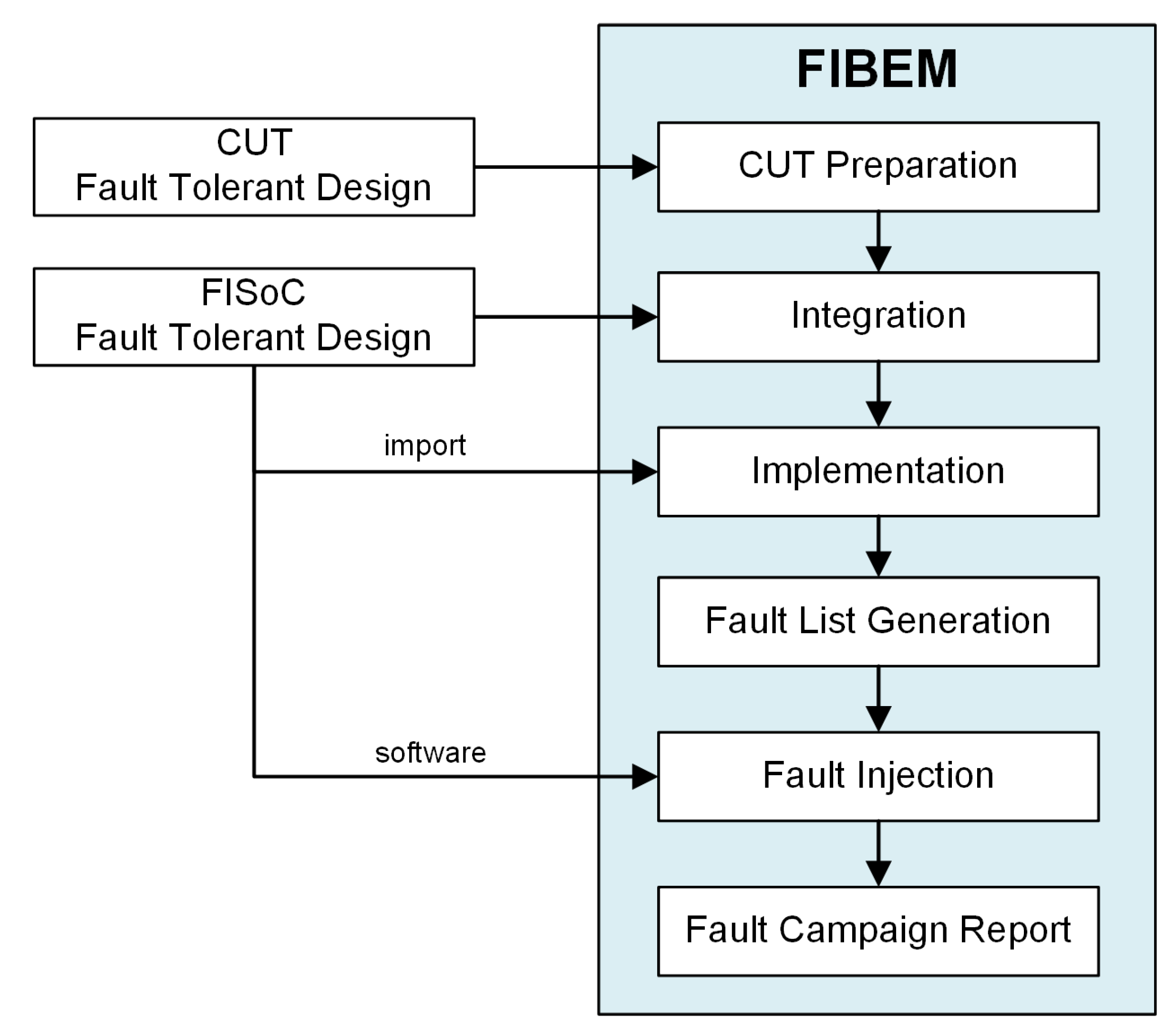
4. Proposed Fault Emulation Flow
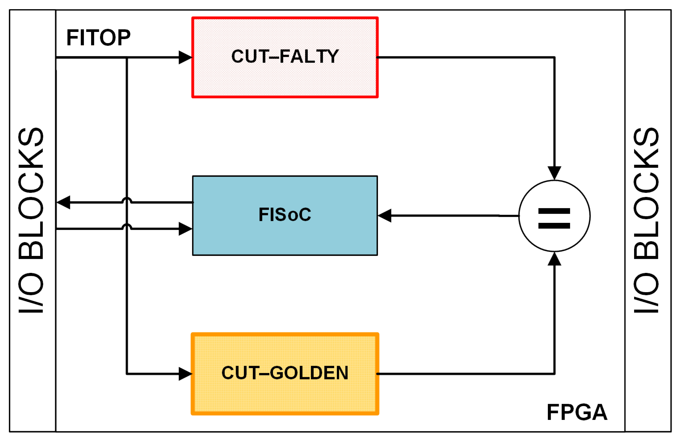
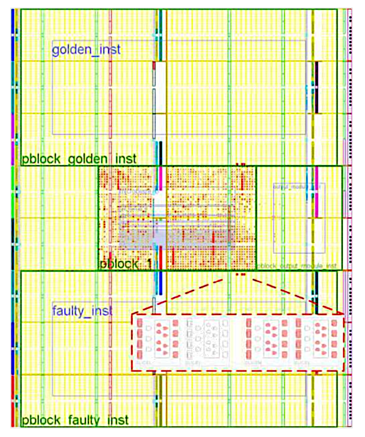
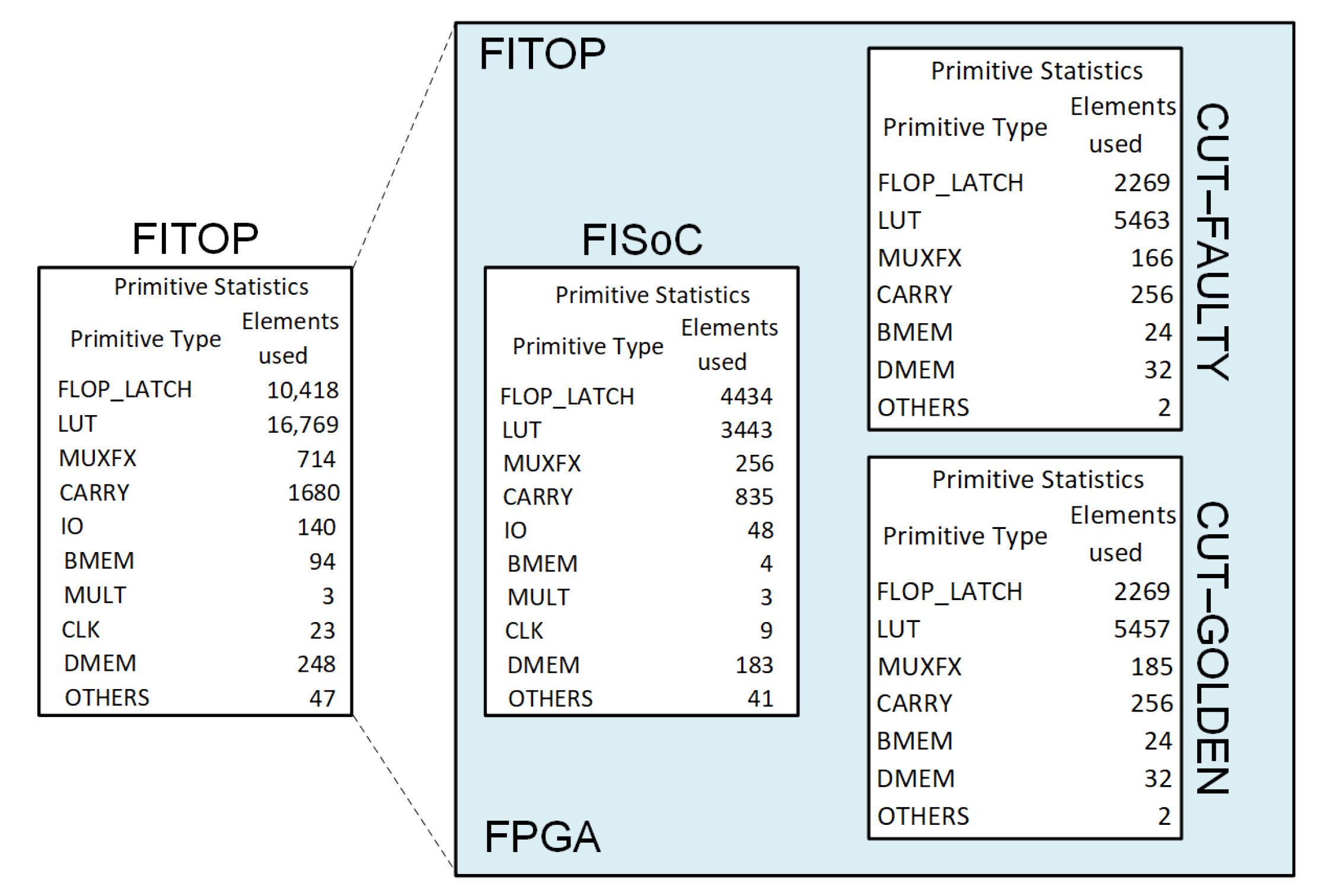
The methodology proposed in this paper is FIBEM, and its flow is presented in Figure 7. This section details the steps of FIBEM flow.

4.1. CUT Prepare

The flow starts with the CUT preparation by removing interface-specific components of the FPGA, which may have been explicitly instantiated inside the CUT. This allows having two CUT instances in the Fault Injection Top (FITOP) module presented in Figure 8. After its logical synthesis, the prepared CUT is instantiated twice (GOLDEN and FAULTY) in FITOP.

4.2. Integration

The two CUT instances are integrated with the Fault Injection System on Chip (FISoC) inside the FITOP. The output ports from the two CUT instances are connected to a comparator module, which should be as generic as possible to simplify its integration with any CUT output.
In order to emulate each fault regardless of their order, the FISoC must be able to put the instances of the CUT in a known state before each fault injection. Therefore, FISoC should be able to reset the CUT instances and the comparator.
The CUT and FISoC are asynchronous to each other, thus requiring additional hardware to avoid metastability and constraints to the asynchronous signals for the time analysis. After that, the FITOP is ready to be logically synthesized.

4.3. Implementation

The implementation is performed by using the Xilinx PlanAhead tool, which allows the loading of the netlists of the module that were logically synthesized in the previous step. PlanAhead allows the definition of physical regions of the FPGA for each module implementation. The area designated for the FAULTY instance of the CUT is constrained to certify that each fault injected solely affects the FAULTY version (Two files, FAULTS.LIST and FAULTS.I, are generated based on mapping the FPGA’s modified components. The FAULTS.I file contains the relevant information for the participation in the fault campaign of the FISoC. Using the Xilinx XPS tool, a FISoC is formed, and the FAULTS.I file is placed into it. Using the ICAP functionality, faults are injected based on the mapping given in the FAULTS.I file. These files result from a previous mapping of other files generated by Xilinx tools and custom libraries to translate and map the netlist provided by the CUT. This netlist mapping serves to render its information visible and manipulable. With this, it is possible to control which regions are affected while avoiding the risk of modifying the FISoC).
The FISoC module does not require any update since it should be reused to reduce the implementation time. Moreover, the FISoC area should be constrained and isolated from the other modules (CUT and comparator) to leverage the rapid prototyping by avoiding the FISoC re-implementation due to any modification (e.g., hardware optimization).
After the implementation stage, PlanAhead generates a netlist containing the entire hardware description that will be configured in the FPGA. This netlist, which is passed to the bitstream generator, has all LUTs used by the implemented design, thus containing the information needed in the next step.

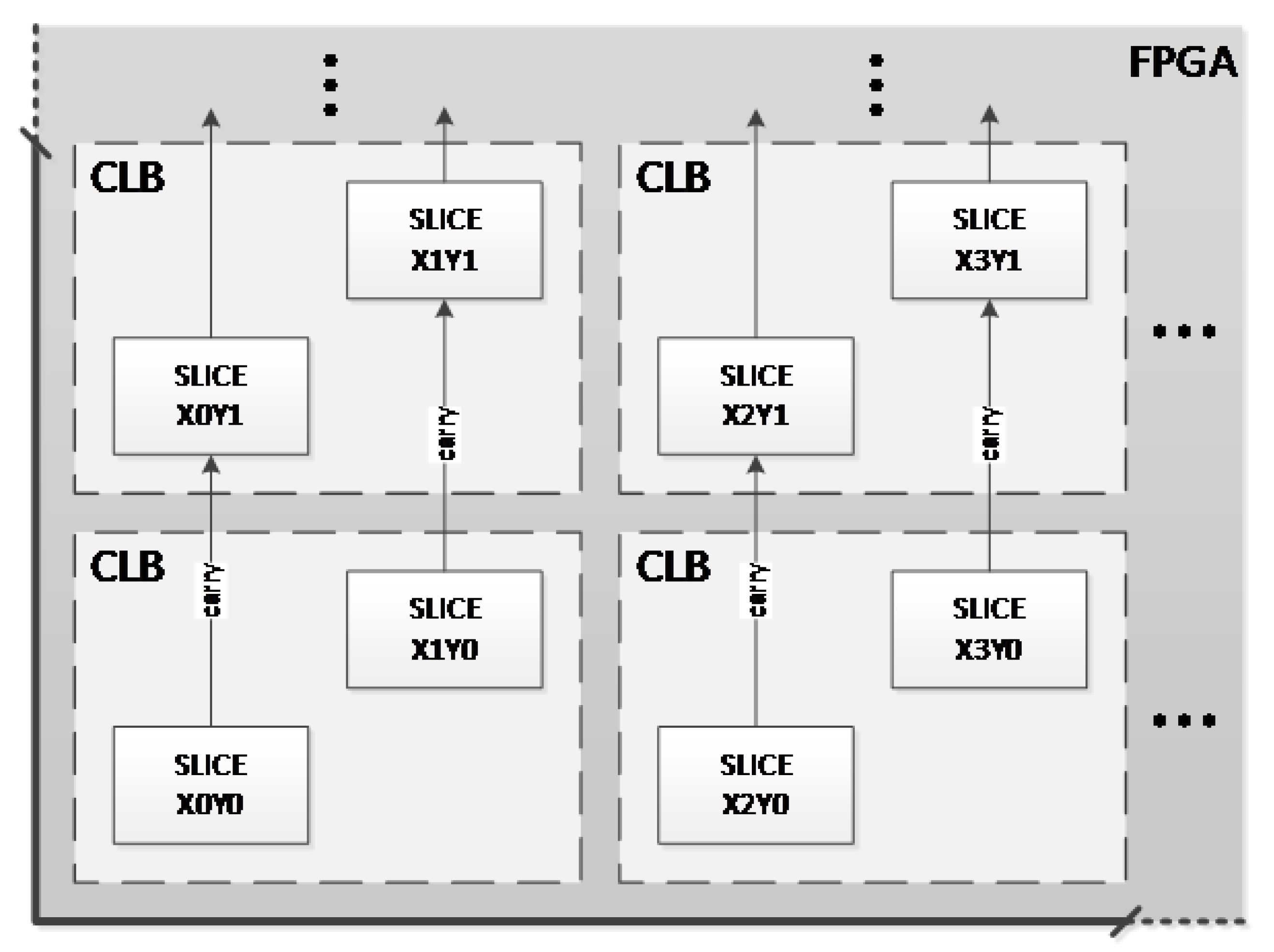
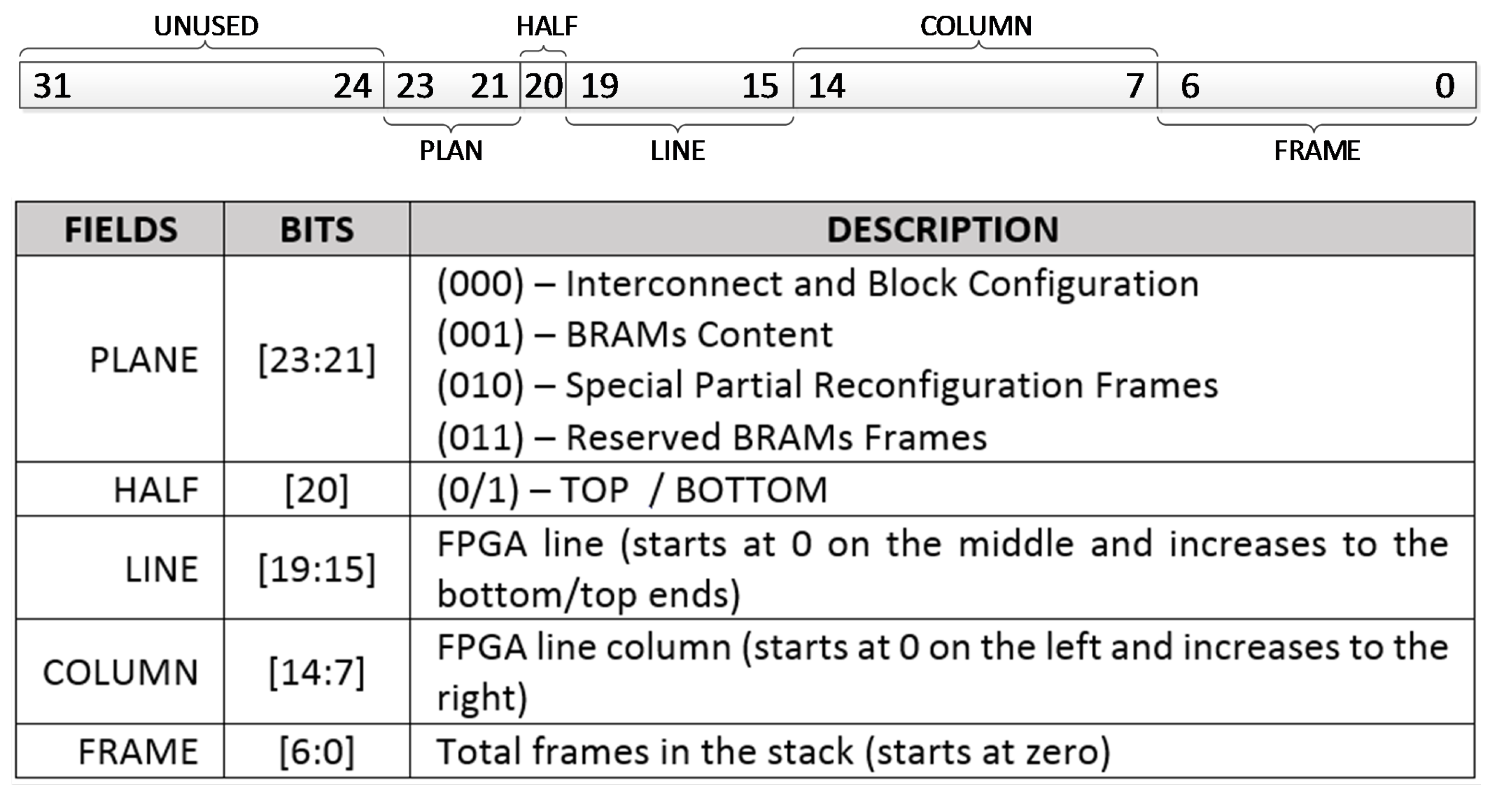
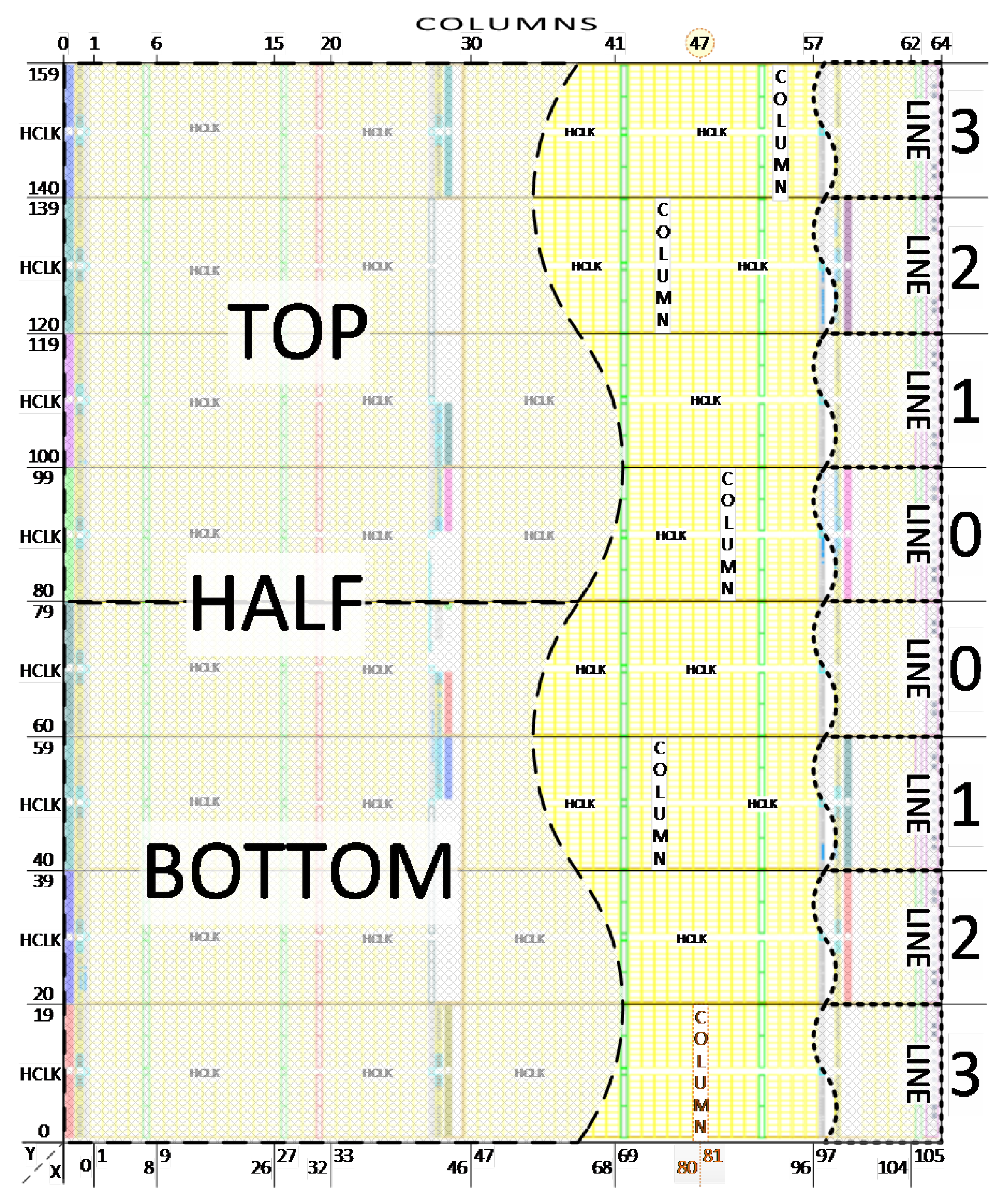
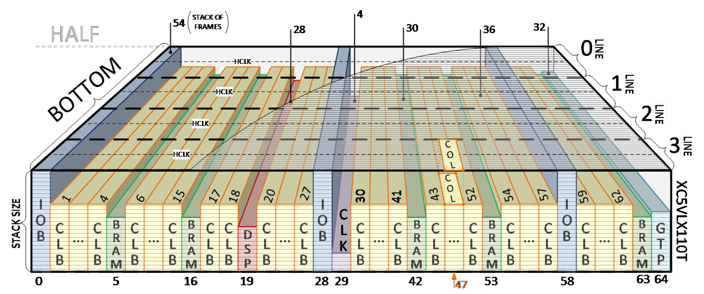
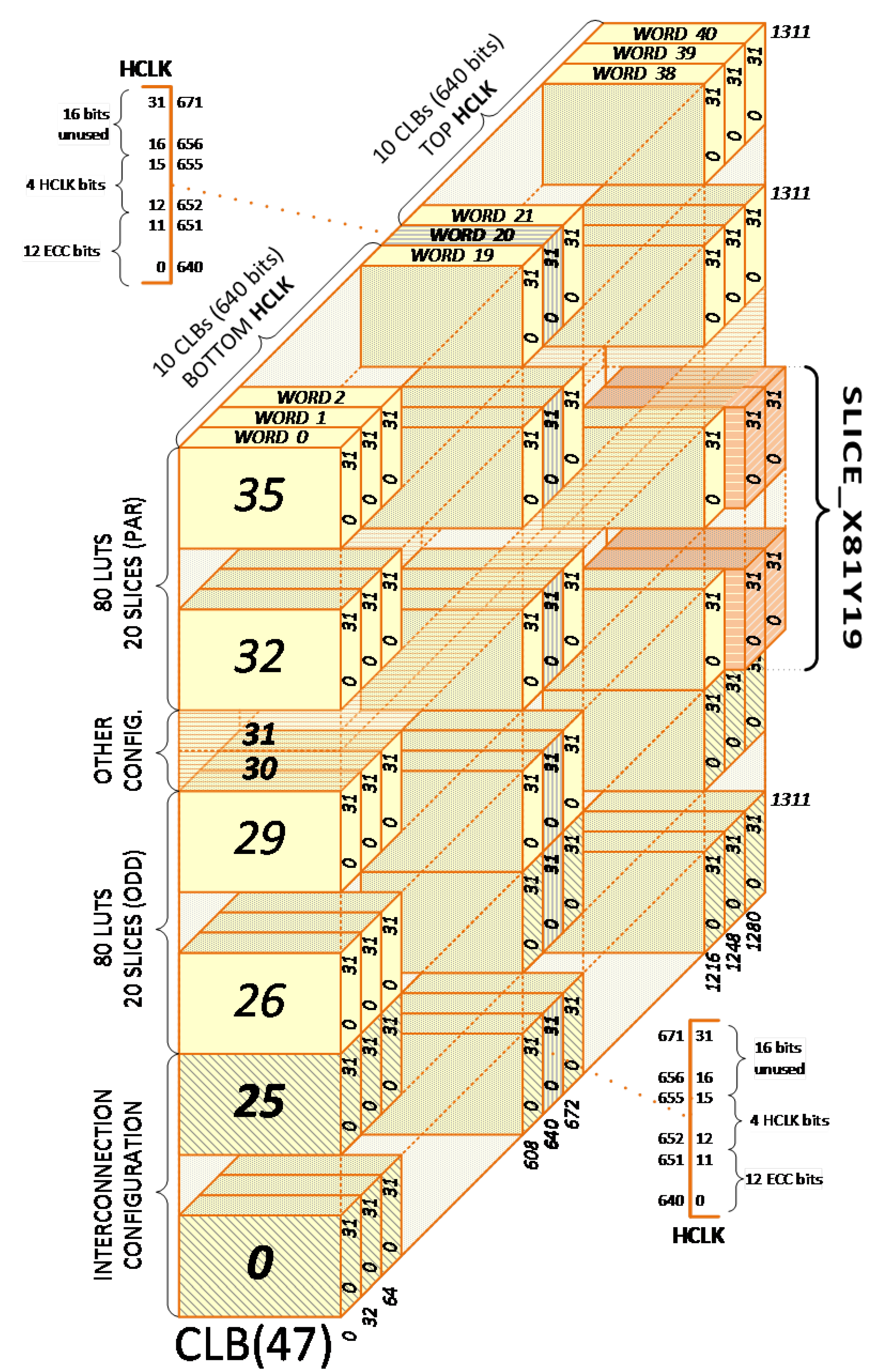
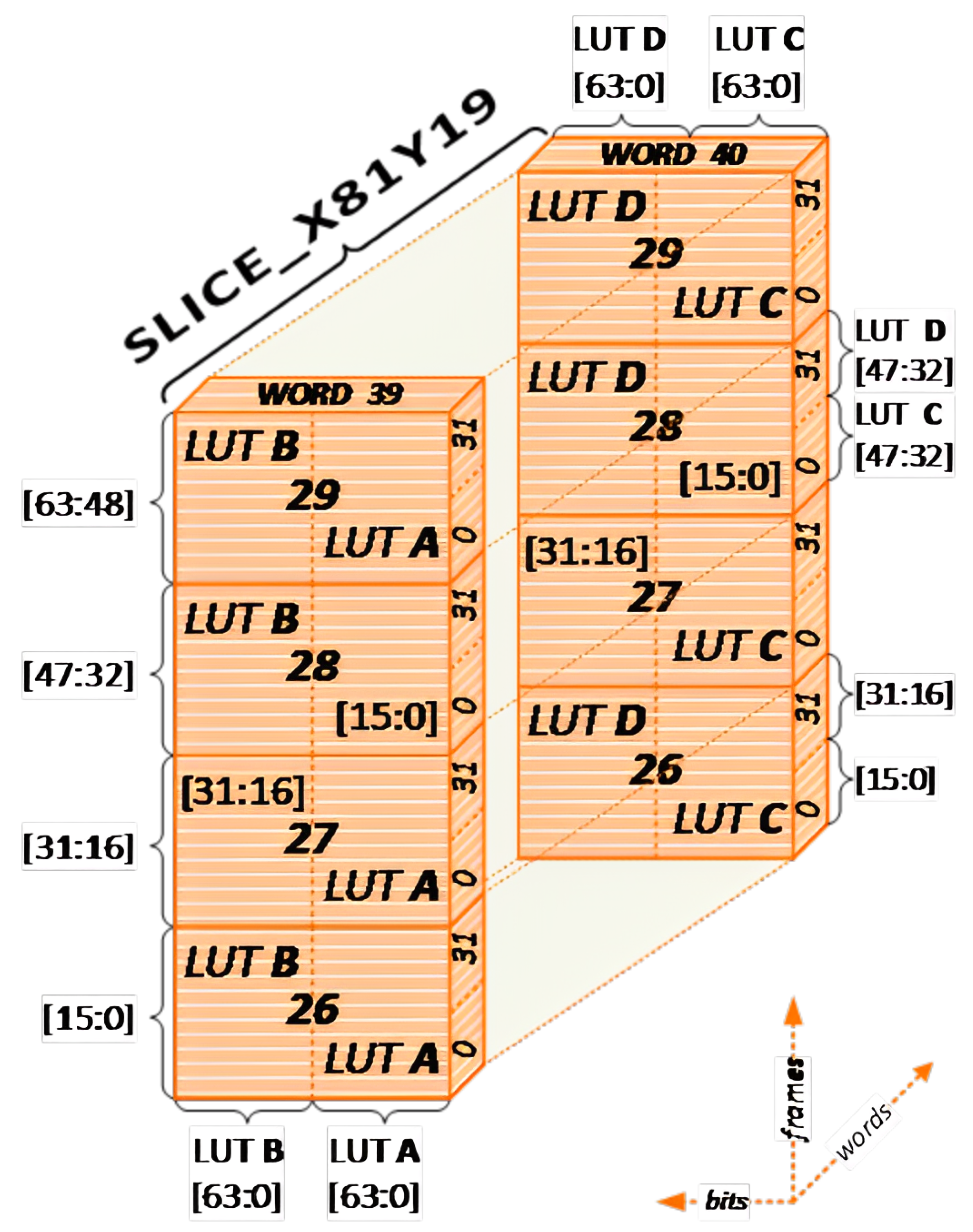
4.4. Fault List Generation

The post-implementation netlist is converted into the Xilinx Design Language (XDL) using the application available at Xilinx installation. XDL has no documentation, though its human-readable language enables identifying FPGA resource configuration (e.g., location of LUTs used by design). The LUTs belonging to the FAULTY version of the CUT can be distinguished by either using its instance-given name or the area constraints defined before the design implementation.
The LUT location provided in the XDL file is expressed in XY coordinates. The thorough FPGA exploration presented in this paper (Section 3) allows the creation of an algorithm that calculates the frame address of the FPGA configuration memory given the LUT XY location. The algorithm returns the first of the four adjacent frames containing the LUT configuration bits for each XY coordinate.
The created algorithm extracts all information of those LUT belonging to the FAULTY instance in the XDL file. This raw information is used for further campaign result reporting. Meanwhile, only the data needed for the fault injection is sent to the FiSoC. The communication between the host and FISoC is reduced by transferring one list with the minimum information required to allow toggling the logic implemented by the LUT.

4.5. Fault Injection

After downloading the FITOP bitstream into the FPGA, the fault list is transferred to FISoC. Before each fault injection, FISoC resets both CUT instances to a known fault-free state to generate and analyze SEEs.
A SET is emulated via toggling the logic implemented by a LUT. For that, FISoC executes four steps: (i) read four frames with the LUT configuration bits; (ii) bitwise invert 16 bits of each frame; (iii) write them back to the configuration memory; and (iv) repeat the last step with the original frames to emulate a SET.
All faults injected are latent/silent by default and emulated until a predefined timer sends a timeout interrupt to FISoC. Whenever the outputs from both CUT instances differ, the comparator triggers a FISoC interruption, which ends the current injection and classifies the fault as an error.

4.6. Fault Coverage Report

FISoC annotates the injection outcome to the fault list, which the host reads after the campaign execution. The host reports the results of each fault injected into the LUTs of the FAULTY instance and summarizes the total faults that are propagated to the outputs or became latent/silent.

4.7. Workflow

The proposed FIBEM flow aims to efficiently evaluate fault tolerance techniques by injecting faults into ICs and observing their response. The flow consists of several steps, including preparing the CUT by creating two instances of it, integrating the CUT with a FISoC and a comparator, implementing the design using the Xilinx PlanAhead tool, generating a fault list using the Xilinx Design Language (XDL), and conducting the fault injection campaign (Algorithm 1).
Algorithm 1: Proposed Fault Emulation Flow.
    
Input: CUT, FISoC, comparator
    
Output: Fault list
Step 1: CUT Preparation;
Remove interface-specific components from CUT;
Instantiate CUT twice (GOLDEN and FAULTY) in FITOP;
Step 2: Integration;
Integrate CUT instances and FISoC in FITOP;
Connect output ports of CUT instances to comparator;
Add hardware to avoid metastability of asynchronous signals;
Step 3: Implementation;
Use PlanAhead tool to load netlists of FITOP modules;
Constrain area for FAULTY instance of CUT;
Generate netlist containing the entire hardware description;
Step 4: Fault List Generation;
Convert netlist to XDL using Xilinx application;
Identify LUTs belonging to FAULTY instance in XDL file;
Use XY coordinates to calculate frame addresses of FPGA configuration     memory;
Extract data needed for fault injection and send to FISoC;
Step 5: Fault Injection;
Use FISoC to reset CUT instances and comparator;
Inject faults into FAULTY instance of CUT using frame addresses;
Observe the response of CUT and record results;
Step 6: Results Analysis;
Analyze results of fault injection to evaluate fault tolerance techniques;
The Fault Injection Framework was designed to experimentally evaluate the fault tolerance techniques designed for critical circuits. The FISoC and both CUT instances (FAULTY and GOLDEN) compose the FITOP (as shown in Figure 9). The FISoC is based on a Xilinx MicroBlaze microcontroller, which has access to the FPGA configuration memory via ICAP.
A FITOP VHDL template with the FISoC instantiation is used to guide adding and connecting the CUT design. The FISoC and the CUT instances are black boxes since they are synthesized previously. The module also compares both CUT instance outputs, which is also part of FITOP.
A Compact Flash card transfers the list of faults to FISoC. The same card is updated with the fault injection results as soon as the campaign has finished. There is no interaction between the FISoC and the host during the fault injection campaign to avoid any communication bottleneck.

5. Experimental Results

5.1. Case Study 1

The FIBEM flow was initially evaluated on a Xilinx example that applies TMR to a simple counter [42]. This example uses 12 LUTs, and a 4 LUTs version without TMR was created to check the applicability of FIBEM flow. Both counter versions were submitted to fault injection, and the results are shown in Table 3 (ICAP allows modifying the content of the truth table of a LUT, thus modifying its logical function. This modification is performed internally to the FPGA and during its operation. In this case, the ICAP configures the TMR feature in the original design). The table compares the results of two different designs for a 4-bit TMR counter. The first design, labeled “Original”, uses TMR to increase the reliability of the circuit by adding redundant copies of the logic gate and the CLB framework for counter-carry logic targeting TMR. The XOR logic gate and the multiplexer, internal to the CLB, propagate the signal between the slices and feed the TMR voter. This allows the use of the CLB structure to infer the desired behavior. In this specific case, the TMR counter uses three copies of the counter circuit to detect and correct errors. Further, it is possible to notice that the original design had no errors and a 100% timeout rate, while the custom design had a 100% error rate and no timeout. Thus, the majority of voters from the TMR technique can prevent errors from propagating to the outputs, while the counter without TMR has all faults injected promptly, causing errors.
Figure 9 depicts the outcome of implementing the four-bit counter with triple redundancy from the Xilinx example, along with the SoCIF located in the middle of the figure. The counter instances FAULTY and GOLDEN are confined at the bottom and the top, respectively. Figure 9 also highlights the implementation result of the FAULTY instance of the CUT, where it is possible to notice the employment of 12 LUTs, 12 registers, and 12 multiplexer/XOR pairs, which corresponds to three carry logics, one from each slice.
Table 4 shows the overhead of adding TMR and carry logic between slices compared to counter without protection and carry. The time required to simulate fault injection using the proposed methodology is just a few seconds. It is noteworthy that the CUT is not expressive in terms of resources used compared to the second case study.

5.2. Case Study 2

The FIBEM flow was applied to an industrial test case of an OnBoard Computer (OBC) for space applications, specified by Instituto Nacional de Pesquisas Espaciais (INPE), National Space Research Institute of Brazil [43]. The fault-tolerant technique uses two redundant FPGAs that process information in parallel. An external circuit decides which FPGA outputs will drive information to the rest of the onboard system. Each FPGA has the SoC based on the Aeroflex Gaisler LEON3 processor, a synthesizable and highly parameterized softcore. The fault-tolerant approach adds a bus monitor to a modified Gaisler SoC version, which works with two LEON3 processors [43]. The additional processor works as a golden reference for the bus monitor, which compares both processors’ outputs. In the case of misbehavior, the bus monitor in both FPGAs (see [43] for more details) alerts the external circuit to avoid error propagation through the system.
The design, as mentioned earlier, required slight updates to work on the FPGA used in this paper. For instance, the original design uses the JTAG to download the program after each restart. Instead, a ROM storing the program executed by LEON3 was used to allow the restarting of the processor at each fault injection.
The FAULTY instance of this CUT was defined as the main Gaisler SoC LEON3, while the redundant processor was used as the GOLDEN reference. The bus monitor output was observed while the faults were injected into the 5425 LUTs of the FAULTY instance, and the results are shown in Table 5. In total, it took 20 min to perform the 5425 injections of faults in this second case study, which is a significant reduction when compared to the 20 h to carry out the injections in the simulation performed.
The estimated count after the logical synthesis of component primitives used by FITOP is shown in Figure 10, where the estimate for the FISoC instance and the CUT instances are also found. This estimate serves to inform the importance of each instance in the use of FPGA resources. It is important to highlight that these values may suffer a decrease due to tool optimizations in the synthesis and implementation.
The OBC monitor was evaluated initially by forcing internal signals during pre-synthesis simulation [43]. This approach explores the behavioral model functionality but ignores the actual hardware elements used to implement the circuit, thus not allowing a proper work comparison between both papers, as pointed out by Table 2, showing results practically opposite to those presented in [43]. Further results using post-synthesis simulation are expected by the authors of [43] and will allow for the performance of a more reliable comparison.
Still, the proposed solution can expose the OBC vulnerability considering the large amount of injected faults propagated and detected by the bus monitor (see Table 2). In other words, a charged particle has a great chance of causing malfunction in one of the FPGAs of the OBC, which must be reset to operate properly again. During the reset process, the space mission can end prematurely if a fault occurs in the redundant FPGA with the same vulnerability features.
The XC5VLX110T device has a configuration memory of more than 30 Mb, accessible by 24,304 frames. Part of those bits are either not writeable or do not even exist. Therefore, the state-of-the-art emulation techniques presented in Section 3, which randomly flip bits over all the configuration memory, could be drastically accelerated by avoiding the injection of ineffective faults. If we compare those techniques by constraining their use to emulate bit-flips on LUT bits (69,120 total with 64 bits each), we would have 0.8 K more faults than the approach presented regarding the OBC test case. This difference increases to more than 36 K when considering the 4-bit TMR counter.

5.3. Discussion

The results presented in Table 3 and Table 5 demonstrate the effectiveness of the proposed fault emulation flow, FIBEM, in evaluating fault tolerance techniques. In the first case study, the counter with TMR prevented any errors from propagating to the outputs, while the counter without TMR had all injected faults causing errors. This demonstrates the efficacy of the TMR technique in ensuring the reliability of the circuit.
In the second case study, the fault tolerance strategy of the OBC using FPGA redundancy was able to detect and prevent any errors from propagating through the system. The results show that FIBEM was able to successfully inject faults into the main Gaisler SoC LEON3 processor, with the redundant processor serving as a reference to detect any errors. This demonstrates the fault tolerance strategy’s effectiveness in ensuring the reliability of the OBC system.
These results highlight the importance of developing efficient methods for evaluating fault tolerance techniques, as they can significantly impact the reliability and robustness of devices and systems. The proposed FIBEM flow offers a promising solution for efficiently evaluating these techniques, and further research can help refine and improve upon this approach.

6. Conclusions

This paper proposes a new fault emulation approach to evaluate fault tolerance techniques. The experimental analyses are performed using partial dynamic reconfiguration via the ICAP feature available on the chosen FPGA. Reconfiguring the FPGA elements that implement the CUT’s combinatorial logic enables the emulation of SET effects on the circuit under test.
This paper shows how the LUT configuration bits are arranged in the FPGAs memory to enable emulating SETs on the combinatorial logic of the CUT. This contribution can drastically reduce the number of faults injected by focusing on the CUT implementation. The presented state-of-the-art approaches randomly emulate bit-flips over all FPGA configurations, thus testing the device instead (which is also performed by the FPGA manufacturer). Therefore, the presented flow could be adapted and applied to other related techniques to accelerate their fault injection campaigns.
The proposed fault emulation approach was able to reduce the number of faults injected during the evaluation of a fault tolerance technique. In the case study presented in this paper, the traditional approach would have injected faults randomly over all the FPGA configuration bits. In contrast, the proposed approach only injected faults into the LUTs belonging to the CUT implementation. This reduction in the number of injected faults significantly improved the execution time of the fault injection campaign. Additionally, the results showed that the proposed approach effectively evaluated the fault tolerance technique, as it identified the faults that caused functional failures in the circuit. These results demonstrate the potential of the proposed approach to accelerate the evaluation of fault tolerance techniques, making it a valuable tool for designers looking to incorporate fault tolerance into their designs.
In summary, the proposed approach reduces the number of faults injected by focusing on the CUT implementation, thus improving execution time and fault coverage results. The proposed flow can be adapted and applied to other related techniques to accelerate fault injection campaigns. Further research and analysis will be performed to evaluate the effectiveness of the approach with other fault models and emulation techniques to support the evaluation of fault-tolerant circuits early in the design process.
For future works, it is planned to expand the methodology to new Xilinx FPGA families, along with studies on carrying out fault injection on other FPGA resources.

Author Contributions

Writing—original draft, software, F.F.; Writing—review and editing, formal analysis, L.O.S.; Writing—review and editing, F.V.; Writing—review and editing, H.P.; Supervision, E.A.B.; Funding, V.R.Q.L. All authors have read and agreed to the published version of the manuscript.

Funding

This work was supported by National Funds through the Fundação para a Ciência e a Tecnologia, I.P. (Portuguese Foundation for Science and Technology) by the Project “VALORIZA—Research Center for Endogenous Resource Valorization” under Grant UIDB/05064/2020 and Grant UIDB/04111/2020.

Data Availability Statement

Data sharing not applicable.

Conflicts of Interest

The funders had no role in the design of the study; in the collection, analyses, or interpretation of data; in the writing of the manuscript; or in the decision to publish the results.

References

  1. Makowski, D. The Impact of Radiation on Electronic Devices with the Special Consideration of Neutron and Gamma Radiation Monitoring; Lodz University of Technology: Łódź, Poland, 2006; pp. 1–151. [Google Scholar]
  2. Reyneri, L.M.; Serrano-Cases, A.; Morilla, Y.; Cuenca-Asensi, S.; Martínez-Álvarez, A. A Compact Model to Evaluate the Effects of High Level C++ Code Hardening in Radiation Environments. Electronics 2019, 8, 653. [Google Scholar] [CrossRef]
  3. Wang, T.; Wan, X.; Jin, H.; Li, H.; Sun, Y.; Liang, R.; Xu, J.; Zheng, L. Optimization of the Cell Structure for Radiation-Hardened Power MOSFETs. Electronics 2019, 8, 598. [Google Scholar] [CrossRef]
  4. Díez-Acereda, V.; L. Khemchandani, S.; del Pino, J.; Mateos-Angulo, S. RHBD Techniques to Mitigate SEU and SET in CMOS Frequency Synthesizers. Electronics 2019, 8, 690. [Google Scholar] [CrossRef]
  5. Viel, F.; Silva, L.A.; Valderi Leithardt, R.Q.; Zeferino, C.A. Internet of Things: Concepts, Architectures and Technologies. In Proceedings of the 2018 13th IEEE International Conference on Industry Applications (INDUSCON), Sao Paulo, Brazil, 12–14 November 2018; pp. 909–916. [Google Scholar] [CrossRef]
  6. Shukla, S.; Ray, K.C. Design and ASIC Implementation of a Reconfigurable Fault-Tolerant ALU for Space Applications. In Proceedings of the 2019 IEEE International Symposium on Smart Electronic Systems (iSES) (Formerly iNiS), Rourkela, India, 16–18 December 2019; pp. 156–159. [Google Scholar] [CrossRef]
  7. Simevski, A.; Schrape, O.; Benito, C.; Krstic, M.; Andjelkovic, M. PISA: Power-robust Multiprocessor Design for Space Applications. In Proceedings of the 2020 IEEE 26th International Symposium on On-Line Testing and Robust System Design (IOLTS), Napoli, Italy, 13–15 July 2020; pp. 1–6. [Google Scholar] [CrossRef]
  8. Kameda, T.; Nagata, A.; Kimura, Y.; Imai, R.; Shrestha, P.; Kimura, K.; Yasuda, A.; Watanabe, H. Space Environment Evaluation and Low-Earth-Orbit Demonstration of a Communication Component with a Commercial Transceiver Integrated Circuit. Aerospace 2022, 9, 280. [Google Scholar] [CrossRef]
  9. Paiva, D.; Duarte, J.M.; Lima, R.; Carvalho, M.; Mattiello-Francisco, F.; Madeira, H. Fault injection platform for affordable verification and validation of CubeSats software. In Proceedings of the 2021 10th Latin-American Symposium on Dependable Computing (LADC), Florianópolis, Brazil, 22–26 November 2021; pp. 1–11. [Google Scholar] [CrossRef]
  10. Pitchaimani, B.; Sridharan, M. A novel emulation method to assess the effects of cosmic radiation for avionics SoC using the GA based fault injection hardware. Sādhanā 2022, 47, 1–6. [Google Scholar] [CrossRef]
  11. Eslami, M.; Ghavami, B.; Raji, M.; Mahani, A. A survey on fault injection methods of digital integrated circuits. Integration 2020, 71, 154–163. [Google Scholar] [CrossRef]
  12. de Oliveira, A.B.; Tambara, L.A.; Benevenuti, F.; Benites, L.A.C.; Added, N.; Aguiar, V.A.P.; Medina, N.H.; Silveira, M.A.G.; Kastensmidt, F.L. Evaluating Soft Core RISC-V Processor in SRAM-Based FPGA Under Radiation Effects. IEEE Trans. Nucl. Sci. 2020, 67, 1503–1510. [Google Scholar] [CrossRef]
  13. Braga, G.; Benevenuti, F.; Gonçalves, M.M.; Hernandez, H.G.; Hübner, M.; Brandalero, M.; Kastensmidt, F.; Azambuja, J.R. Evaluating softcore GPU in SRAM-based FPGA under radiation-induced effects. Microelectron. Reliab. 2021, 126, 114348, In Proceedings of ESREF 2021, 32nd European Symposium on Reliability of Electron Devices, Failure Physics and Analysis, Virtually, 4–8 October 2021. [Google Scholar] [CrossRef]
  14. Ding, Q.; Luo, R.; Wang, H.; Yang, H.; Xie, Y. Modeling the Impact of Process Variation on Critical Charge Distribution. In Proceedings of the 2006 IEEE International SOC Conference, Austin, TX, USA, 24–27 September 2006; Volume 2, pp. 243–246. [Google Scholar] [CrossRef]
  15. Mogollon, J.M.; Guzman-Miranda, H.; Napoles, J.; Aguirre, M.A. Metrics for the Measurement of the Quality of Stimuli in Radiation Testing Using Fast Hardware Emulation. IEEE Trans. Nucl. Sci. 2013, 60, 2456–2460. [Google Scholar] [CrossRef]
  16. Dodd, P.; Massengill, L. Basic mechanisms and modeling of single-event upset in digital microelectronics. IEEE Trans. Nucl. Sci. 2003, 50, 583–602. [Google Scholar] [CrossRef]
  17. Lesea, A.; Drimer, S.; Fabula, J.; Carmichael, C.; Alfke, P. The Rosetta Experiment: Atmospheric Soft Error Rate Testing in Fiffering Technology FPGAs. IEEE Trans. Device Mater. Reliab. 2005, 5, 317–328. [Google Scholar] [CrossRef]
  18. Bocquillon, A.; Foucard, G.; Miller, F.; Buard, N.; Leveugle, R.; Daniel, C.; Rakers, S.; Carriere, T.; Pouget, V.; Velazco, R. Highlights of laser testing capabilities regarding the understanding of SEE in SRAM based FPGAs. In Proceedings of the 2007 9th European Conference on Radiation and Its Effects on Components and Systems, Deauville, France, 10–14 September 2007; pp. 1–6. [Google Scholar] [CrossRef]
  19. Padmapriya, K.; Varaprasad, B. Improving Test Coverage of Hi-Reliability ASIC Designs with Test Point Insertion for Space Applications. In Proceedings of the 2020 International Conference on Smart Electronics and Communication (ICOSEC), Trichy, India, 10–12 September 2020; pp. 1099–1103. [Google Scholar] [CrossRef]
  20. Ziade, H.; Ayoubi, R.; Velazco, R. A Survey on Fault Injection Techniques. Int. Arab. J. Inf. Technol. 2004, 1, 171–186. [Google Scholar] [CrossRef]
  21. da Silva, A.; Sanchez, S. LEON3 ViP: A Virtual Platform with Fault Injection Capabilities. In Proceedings of the 2010 13th Euromicro Conference on Digital System Design: Architectures, Methods and Tools, Lille, France, 1–3 September 2010; pp. 813–816. [Google Scholar] [CrossRef]
  22. Jenn, E.; Arlat, J.; Rimen, M.; Ohlsson, J.; Karlsson, J. Fault injection into VHDL models: The MEFISTO tool. In Proceedings of the IEEE 24th International Symposium on Fault- Tolerant Computing, Austin, TX, USA, 15–17 June 1994; Volume 2, pp. 66–75. [Google Scholar] [CrossRef]
  23. Lopez-Ongil, C.; Garcia-Valderas, M.; Portela-Garcia, M.; Entrena, L. Autonomous Fault Emulation: A New FPGA-Based Acceleration System for Hardness Evaluation. IEEE Trans. Nucl. Sci. 2007, 54, 252–261. [Google Scholar] [CrossRef]
  24. Entrena, L.; Garcia-Valderas, M.; Fernandez-Cardenal, R.; Lindoso, A.; Portela, M.; Lopez-Ongil, C. Soft Error Sensitivity Evaluation of Microprocessors by Multilevel Emulation-Based Fault Injection. IEEE Trans. Comput. 2010, 61, 313–322. [Google Scholar] [CrossRef]
  25. Vanhauwaert, P.; Leveugle, R.; Roche, P. Reduced Instrumentation and Optimized Fault Injection Control for Dependability Analysis. In Proceedings of the 2006 IFIP International Conference on Very Large Scale Integration, Nice, France, 16–18 October 2006; pp. 391–396. [Google Scholar] [CrossRef]
  26. Alderighi, M.; Casini, F.; D’Angelo, S.; Mancini, M.; Codinachs, D.M.; Pastore, S.; Poivey, C.; Sechi, G.R.; Weigand, G.S.R. Experimental validation of fault injection analyses by the FLIPPER tool. In Proceedings of the 2009 European Conference on Radiation and Its Effects on Components and Systems, Brugge, Belgium, 14–18 September 2009; Volume 57, pp. 544–548. [Google Scholar] [CrossRef]
  27. Alderighi, M.; Casini, F.; D’Angelo, S.; Pastore, S.; Sechi, G.; Weigand, R. Evaluation of Single Event Upset Mitigation Schemes for SRAM based FPGAs using the FLIPPER Fault Injection Platform. In Proceedings of the 22nd IEEE International Symposium on Defect and Fault-Tolerance in VLSI Systems (DFT 2007), Rome, Italy, 26–28 September 2007; pp. 105–113. [Google Scholar] [CrossRef]
  28. Aguirre, M.; Tombs, J.; Muñoz, F.; Baena, V.; Torralba, A.; Fernández-León, A.; Tortosa, F.; González-Gutiérrez, D. An FPGA Based Bardware Emulator for the Insertion and Analysis of Single Event Upsets in VLSI Designs. Radiation Effects on Components and Systems Workshop (RADECS). 2004, pp. 1–5. Available online: https://www.tib.eu/en/search/id/BLCP%3ACN058079892/A-FPGA-based-hardware-emulator-for-the-insertion/ (accessed on 25 December 2022).
  29. Dutton, B.; Ali, M.; Sunwoo, J.; Stroud, C. Embedded Processor Based Fault Injection and SEU Emulation for FPGAs. In Proceedings of the International Conference on Embedded Systems and Applications, Las Vegas, NV, USA, 14 July 2009; pp. 183–189. [Google Scholar]
  30. Serrano, F.; Alaminos, V.; Clemente, J.; Mecha, H.; Liu, S. NESSY: Una plataforma de inyección de errores para una FPGA Virtex-5. JCRA. 2012. Available online: https://jornadassarteco.org (accessed on 25 December 2022).
  31. Chapman, K. SEU Strategies for Virtex-5 Devices; Xilinx Inc.: San Jose, CA, USA, 2010; Volume 2.0, pp. 1–16. [Google Scholar]
  32. Ferlini, F.; Seman, L.O.; Bezerra, E.A. Enabling ISO 26262 Compliance with Accelerated Diagnostic Coverage Assessment. Electronics 2020, 9, 732. [Google Scholar] [CrossRef]
  33. Leipnitz, M.T.; Geferson, L.; Nazar, G.L. A fault injection platform for fpga-based communication systems. In Proceedings of the 2016 IEEE 7th Latin American Symposium on Circuits & Systems (LASCAS), Florianopolis, Brazil, 28 February–2 March 2016; pp. 59–62. [Google Scholar]
  34. Zhang, R.; Xiao, L.; Li, J.; Cao, X.; Qi, C.; Li, J.; Wang, M. A fast fault injection platform of multiple SEUs for SRAM-based FPGAs. Microelectron. Reliab. 2018, 82, 147–152. [Google Scholar] [CrossRef]
  35. Xie, Y.; Chen, H.; Xie, Y.Z.; Mao, C.A.; Li, B.Y. An automated FPGA-based fault injection platform for granularly-pipelined fault tolerant CORDIC. In Proceedings of the 2018 International Conference on Field-Programmable Technology (FPT), Naha, Japan, 10–14 December 2018; pp. 370–373. [Google Scholar]
  36. Wilson, A.E.; Wirthlin, M. Fault Injection of TMR Open Source RISC-V Processors using Dynamic Partial Reconfiguration on SRAM-based FPGAs. In Proceedings of the 2021 IEEE Space Computing Conference (SCC), Laurel, MD, USA, 23–27 August 2021; pp. 1–8. [Google Scholar]
  37. Zhang, Y.; Chen, L.; Wang, S.; Zhou, J.; Tian, C.; Feng, H. Research on agile FPGA fault injection system. In Proceedings of the 2021 International Conference on Microelectronics (ICM), New Cairo City, Egypt, 19–22 December 2021; pp. 57–61. [Google Scholar]
  38. Yang, W.; Li, Y.; He, C. Fault injection and failure analysis on Xilinx 16 nm FinFET Ultrascale+ MPSoC. Nucl. Eng. Technol. 2022, 54, 2031–2036. [Google Scholar] [CrossRef]
  39. Feng, H.; Li, W.; Chen, L.; Wang, S.; Zhou, J.; Tian, C.; Zhang, Y. Precise Fault Injection and Fault Location System for SRAM-based FPGAs. In Proceedings of the 2022 IEEE 10th Joint International Information Technology and Artificial Intelligence Conference (ITAIC), Chongqing, China, 17–19 June 2022; Volume 10, pp. 2371–2376. [Google Scholar]
  40. Xilinx. Virtex-5 FPGA Configuration User Guide; Xilinx Inc.: San Jose, CA, USA, 2012; Volume 3.11, pp. 1–166. [Google Scholar]
  41. Xilinx. Virtex-5 FPGA User Guide; Xilinx Inc.: San Jose, CA, USA, 2012; Volume 5.4, pp. 1–385. [Google Scholar]
  42. Carmichael, C. Application Note: Virtex Series Triple Module Redundancy Design Techniques for Virtex FPGAs TMR in FPGAs; Xilinx Inc.: San Jose, CA, USA, 2006; Volume 1.0.1, pp. 1–37. [Google Scholar]
  43. Ferlini, F.; da Silva, F.A.; Bezerra, E.A.; Lettnin, D.V. Non-intrusive fault tolerance in soft processors through circuit duplication. In Proceedings of the LATW ’12: Proceedings of the 2012 13th Latin American Test Workshop, Washington, DC, USA, 10–13 April 2012; pp. 1–6. [CrossRef]
Figure 3. Coordinate system versus addressing system.
Electronics 12 00807 g003
Figure 4. Bottom view perspective of FPGA configuration memory.
Electronics 12 00807 g004
Figure 5. Stack of the column (47) that is CLB type.
Electronics 12 00807 g005
Figure 6. Stack of the column (47) that is CLB type.
Electronics 12 00807 g006
Figure 7. FIBEM flow.
Electronics 12 00807 g007
Figure 8. FITOP with the FISoC, the comparator and the two CUT instances.
Electronics 12 00807 g008
Figure 9. Counter with the area of the established GOLDEN and FAULTY instances.
Electronics 12 00807 g009
Figure 10. Estimated amount of components used in FITOP, FISoC, and by the two CUT instances (FAULTY and GOLDEN).
Electronics 12 00807 g010
Table 1. Summary of the main points and features of the reviewed papers.
PaperMethodProsCons
[1]Physical injection (particle radiation or laser beam)Realistic resultsExpensive, requires specific equipment
[17]Physical injection (particle radiation or laser beam)Realistic resultsExpensive, requires specific equipment
[18]Physical injection (particle radiation or laser beam)Realistic resultsExpensive, requires specific equipment
[20]Physical injection (pin forcing) Limited to IC boundaries, requires a prototype
[21]Simulation-based injection (SystemC transaction level model)Early analysisHigh computing resources, long execution time
[22]Simulation-based injection (VHDL model) High computing resources, long execution time
[23]Emulation-based injection (autonomous technique)Reduced execution timeIntrusive approach
[24]Emulation-based injection (autonomous technique)Reduced execution timeIntrusive approach
[25]Emulation-based injection (autonomous technique)Reduced execution timeIntrusive approach
[26]Emulation-based injection (partial reconfiguration)Non-intrusive approachLimited to Xilinx FPGAs
[15]Emulation-based injection (partial reconfiguration)Non-intrusive approachLimited to Xilinx FPGAs
Table 2. Summary of frames needed to configure the FPGA regarding the resource types and the layers (abstraction of the configuration memory).
#Layer (#)/
Block Type
Stack
Size
Total of
Columns
Frames per
Line
Total FPGA FramesTotal .BIT
Frames
0IOB543162129618,576
CLB3654194415,552
BRAM (config.)3051501200
DSP28128224
GLK41432
GTP32132256
JUMP21216
1BRAM (data)128564051205136
JUMP21216
2PARTIAL (rect.)16565520
JUMP21216
3RESERVED15540
JUMP21216
Total FPGA Frames in Configuration Memory24,30423,712
Table 3. Fault injection results regarding the counter with TMR case study.
Total
LUTs
Case Study 1—TMR Counter 4 Bits
Design DescriptionERRORTIMEOUT
12Original—Counter
with TMR
0%100%
4Custom—Counter
without TMR
100%0%
Table 4. Utilization of XC5VLX110T FPGA resources and overhead by counter with TMR and carry in comparison with counter without TMR and carry.
  Resource Elements Used
Original Model
Elements Used
without TMR
and Carry
  Overhead of
the Original
  Total of
Elements
ICAPs110.00%2
DSP48Es330.00%64
Slices184218470.00%17,280
Slice Registers
(as FF)
418541690.38%69,120
Slice Registers
(as LatchThrus)
440.00%
Slice LUTs356735570.28%69,120
Slice LUT-FF
pairs
356735380.82%69,120
Table 5. Fault injection results regarding the OBC case study.
Total LUTs
5425
Case Study 2—OBC with the Bus Monitor
Fault Injection Result DescriptionTotal%
ErrorFaults
propagated to
the outputs
3916 72
Silent/LatentFaults that
become latent
silent
1509 18
Disclaimer/Publisher’s Note: The statements, opinions and data contained in all publications are solely those of the individual author(s) and contributor(s) and not of MDPI and/or the editor(s). MDPI and/or the editor(s) disclaim responsibility for any injury to people or property resulting from any ideas, methods, instructions or products referred to in the content.

